

6/94
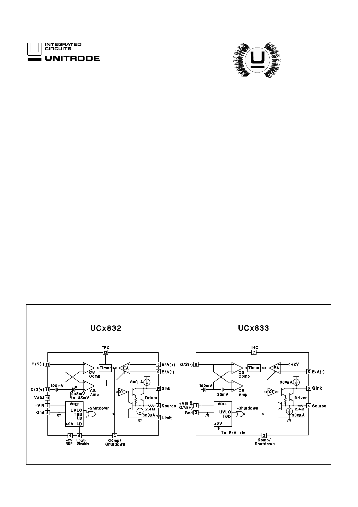
BLOCK DIAGRAMS
• Precision 1% Reference
• Over-Current Sense Threshold
Accurate to 5%
• Programmable Duty-Ratio
Over-Current Protection
• 4.5V to 36V Operation
• 100mA Output Drive, Source or
Sink
• Under-Voltage Lockout
Additional Features of the UC1832
series:
• Adjustable Current Limit to
Current Sense Ratio
• Separate +V
IN terminal
• Programmable Driver Current
Limit
• Access to V
REF
and E/A(+)
• Logic-Level Disable Input
The UC1832 a nd UC18 33 series of precisio n line ar regulato rs includ e all the
control functions re quired in the design o f very low dropout linear regulators.
Additionally, they feature an innovative duty-ratio current limiting technique
which provides peak load capab ility while limiting the average power dissipation of the external pass transistor during fault conditions. When the load current reaches an accurately programmed threshold, a gated-astable timer is
enabled, which switches the regulator’s pass device off and on at an externally
programmable duty-ratio. During the on-time of the pass element, the output
current is limited to a value slightly higher than the trip threshold of the duty-ratio timer. The constant-current-limit is programmable on the UCx832 to allow
higher peak current during the on-time of the pass device. With duty-ratio control, high initial load demands and short circuit protection may both be accommodated without extra heat sinki ng or foldback current limiting. Additionally, if
the timer pin is grounded, the du ty-ratio timer is disabled, and the IC operates
in constant-voltage/constant-current regulating mode.
These IC’s include a 2 Volt (±1%) reference, error amplifier, UVLO, and a high
current driver that has both source and sink outputs, allowing the use of either
NPN or PNP external pass transistors. Safe operation is assured by the inclusion of under-voltage lockout (UVLO) and thermal shutdown.
The UC1833 family includes the basic functions of this design in a low-cost, 8pin mini-di p package , whi le the UC 1832 seri es provides added versatility with
the availability o f 14 pins. Packagi ng options include plastic (N suffix), or ceramic (J suffix). Specified opera ting tempe rature ranges are: commercial (0°C
to 70°C), order UC3832/3 (N or J); industrial (–25°C to 85°C), order UC2832/3
(N or J); and military (–55°C to 125°C), order UC1832/3J. Surface mount
packaging is also available.
UC1832/3
UC2832/3
UC3832/3
Precision Low Dropout Linear Controllers
FEATURES DESCRIPTION
UDG-92040
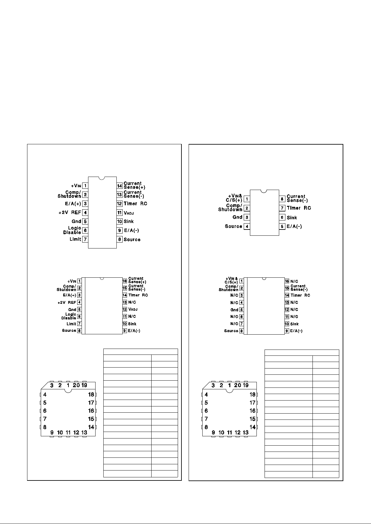
CONNECTION DIAG RAMS
DIL-14 (Top Vi ew )
J Or N Package
SOIC-16 (Top View)
DW Package
UC1832/3
UC2832/3
UC3832/3
PACKAGE PIN FUNCTION
FUNCTION PIN
N/C 1
+V
IN 2
Comp/Shutdown 3
E/A(+) 4
+2V REF 5
N/C 6
Gnd 7
Logic Disable 8
Limit 9
Source 10
N/C 11
E/A(-) 12
Sink 13
V
ADJ 14
N/C 15-17
Timer RC 18
Current Sense(- ) 19
Current Sense(+) 20
LCC-20 & PLCC-20
L & Q Package
(Top View)
ABSOLUTE MAXIMUM RATINGS
Supply Voltage +VIN. . . . . . . . . . . . . . . . . . . . . . . . . . . . . . . 40V
Driver Output Curren t (S ink or Source) . . . . . . . . . . . . . 450mA
Driver Sink to Source Voltage . . . . . . . . . . . . . . . . . . . . . . . 40V
TRC Pin Voltage. . . . . . . . . . . . . . . . . . . . . . . . . . –0. 3V to 3.2V
Other Input Vol tages. . . . . . . . . . . . . . . . . . . . . . . –0.3V t o +V
IN
Operating Jun ctio n Tem per atur e (no te 2) . . . –55°C to +150° C
Storage Temperature. . . . . . . . . . . . . . . . . . . –65°C to +150°C
Lead Temperat ure (Solde ring, 10 Sec onds ) . . . . . . . . . . 300°C
Note 1: Unless otherwise indica te d, voltages ar e re feren ced t o
ground and curre nts are posit ive into , negat ive out of, the specified terminals.
Note 2: See Unitrod e Inte gra ted C ircuit s datab ook f or
information regar ding t her m al specif icat ions an d limita tion s of
packages.
UC1832 UC1833
PACKAGE PIN FUNCTION
FUNCTION PIN
+VIN & C/S(+) 1
N/C 2
N/C 3
N/C 4
Comp/Shutdown 5
Gnd 6
N/C 7
N/C 8
N/C 9
Source 10
N/C 11
E/A(-) 12
N/C 13
N/C 14
Sink 15
Timer RC 16
Current Sense(+) 17
N/C 18-2 0
SOIC-16 (Top View)
DW Package
DIL-8 (Top View)
J Or N Package
LCC-20 & PLCC-20
L & Q Package
(Top View)
2
PARAMETER TEST CONDITIONS MIN TYP MAX UNITS
Input S u p pl y
Supply Curren t +V
IN = 6V 6.5 10 mA
+V
IN = 36V 9.5 15 mA
Logic Disable = 2V (UCx832 only) 3.3 mA
Reference Sect ion
Output Volta g e (Not e 3) T
J = 25°C, I DRIVER = 10mA 1.98 2.00 2.02 V
over temperature, I
DRIVER = 10mA 1.96 2.00 2.04 V
Load Regulat io n (UCx8 32 only) I
OUT = 0 to 10mA -10 -5.0 mV
Line Regulation +VIN = 4.5 to 36V, IDRIVER = 10mA 0.033 0.5 mV/V
Under-Voltage Lockout Threshold 3.6 4 .5 V
Logic Disabl e I npu t (UCx 832 on ly )
Threshold Volt age 1.3 1.4 1.5 V
Input Bias Current Logic Disable = 0V -5.0 -1.0 µA
Current Sense Section
Comparator Offset 95 100 105 mV
Over Temperature 93 100 107 mV
Amplifier Offset (UCx833 only) 110 135 170 mV
Amplifier Offset (UCx832 only) V
ADJ = Open 110 135 170 mV
V
ADJ = 1V 180 235 290 mV
V
ADJ = 0V 250 305 360 mV
Input Bias Current V
CM = +VIN 65 100 135 µA
Input Offset Current (UCx832 only) V
CM = +VIN -10 10 µA
Amplifier CMRR (UCx83 2 only) V
CM = 4.1V to +VIN+0.3V 80 dB
Transcon ductance I
COMP =
±
100µA65mS
VADJ Input Current (UCx832 only) VADJ = 0V -10 -1 µA
Timer
Inactive Leakage Current C/S(+) = C/S(-) = +V
IN; TRC pin = 2V 0.25 1.0 µA
Active Pullup Current C/S(+) = +V
IN, C/S(-) = +VIN - 0.4V; TRC pin = 0V -345 -270 -175 µA
Duty Ratio (not e 4) ontime/period , R
T = 200k, C T = 0.27µ F4.8 %
Period (not es 4, 5) ontime + offtime, R
T = 200k, CT = 0.27 µF 36 ms
Upper Trip Thr esh old (Vu) 1.8 V
Lower Trip Thresh old (Vl) 0.9 V
Trip Thresh old Rat io Vu/Vl 2.0 V/V
Error Amplifi er
Input Offset Voltage (UCx832 only) V
CM = VCOMP = 2 V -8.0 8.0 mV
Input Bias Current V
CM = VCOMP = 2 V -4.5 -1.1 µA
Input Offset Current (UCx832 only) V
CM = VCOMP = 2 V -1.5 1.5 µA
AVOL V
COMP = 1V to 13V 50 70 dB
CMRR (UCx832 only) V
CM = 0V to +VIN - 3V 60 80 dB
PSRR (UCx832 only) V
CM = 2V, +VIN = 4.5 to 36V 90 dB
Transcon duct ance ICOMP = ±10µA4.3mS
VOH I
COMP = 0, Volts below +V IN .95 1.3 V
VOL I
COMP = 0 .45 0.7 V
IOH V
COMP = 2V -700 -500 -100 µA
UC1832/3
UC2832/3
UC3832/3
Unless otherwise stated, specifications hold for TA = 0°C to 70°C for the
UC3832/3, –25°C to 85°C for the UC2832/3, and –55°C to 125°C for the
UC1832/3, +VIN = 15V, Driver sink = +V IN, C/S(+) voltage = +VIN. TA=TJ.
ELECTRICAL CHARACTERISTICS:
3

Unless otherwise stated, specifications hold for TA = 0°C to 70°C for the UC3832/3, –25°C to
85°C for the UC2832/3, and –55°C to 125°C for the UC1832/3, +VIN = 15V, Driver sink =
+VIN, C/S(+) voltage = +V IN. TA=TJ.
ELECTRICAL
CHARACTERISTICS (cont.)
UC1832/3
UC2832/3
UC3832/3
PARAMETER TEST CONDITIONS MIN TYP MAX UNITS
Error Amplifi er (cont .)
IOL V
COMP = 2V, C/S(-) = +VIN 100 500 700 µA
VCOMP = 2V, C/S(-) = +VIN - 0.4V 2 6 mA
Driver
Maximum Cur rent Driver Limit & Source pins common; T
J = 25°C 200 300 400 mA
Over Temperature 100 300 450 mA
Limiting Volta ge (UCx 832 on ly) Driver Limit to Source voltage at curre nt limit,
I
SOURCE = -10mA; TJ = 25°C (Note 6) .72 V
Internal Curren t Sen se Resistan ce T
J = 25°C (Note 6) 2.4 Ω
Pull-Up Current at Driver S ink Compensation/Shutdown = 0.4V; Driver Sink = +V
IN - 1V -800 -300 -100 µA
Compensation/Shutdown = 0.4V, +VIN = 36V; D river
Sink = 35V -1000 -300 -75 µA
Pull-Down Curren t at Driver Source Compens atio n/Shut down = 0.4V; Driv er Source = 1V 150 300 700 µA
Saturation Volt age Sink t o Source Driver Source = 0V; Driver Curr ent = 100mA 1.5 V
Maximum Source Volt age Driver Sink = +V
IN, Driver Current = 100mA
Volts below +V
IN 3.0 V
UVLO Sink Leakage +V
IN = C/S(+) = C/S(-) = 2.5V, Driv er Sink = 15V, Driver
Source = 0V, TA = 25°C 25 µA
Maximum Reverse Sourc e Voltage Compensation/ Shut down = 0V; I
SOURCE = 100µA,
+V
IN = 3V 1.6 V
Thermal Shutdo w n 160 °C
Note 3: On the UCx833 this voltage is defined as the r egulat ing leve l at the error amp lifier inverting input, with the error amplifier
driving V
SOURCE
to 2V.
Note 4: These param et ers are first- ord er supply- in depe nden t, howe ver both ma y vary w ith supply for +V
IN
less than about 4V. This
supply variation will cause a slight change in the time r period and duty cycle, althoug h a high off-t ime /on-tim e ratio w ill be maintained.
Note 5: With recom mend ed R
T
value of 200k, T
OFF
≈
RT CT * ln(Vu/Vl) ±10%.
Note 6: The internal cur ren t limiting volt age has a temperat ure depen denc e of appr oxim at ely -2.0m V/ °C, or -2800ppm /°C. The inter nal 2.4
Ω
sense resistor has a tempera tu re depend ance of approxima te ly +1500 ppm / °C.
UDG-92041-1
APPLICATION AND OPERATION INFORMATION
NPN Pass (Local 100mA Regulator) (UCx833)
4

UC1832/3
UC2832/3
UC3832/3
APPLICATION AND OPERATION INFORMATION (cont.)
UDG-92042-1
UDG-92043-1
PNP Pass (Low Drop-Out Regulator) (UCx833)
NPN Pass (Medium Power, Low Drop-Out Regulator) (UCx832)
For any power supply, the rate at which the total output
capacitance can be charged depends on the maximum
output current available and on the nature of the load. For
a constant-current current-limited power supply, the output will come up if the load asks for less than the maximum available short-circuit limit current.
To guarantee recovery of a duty-ratio current-limited
power supply from a short-circuited load condition, there
is a maximum total output capacitance which can be
charged for a given unit ON time. The design value of ON
time can be adjusted by changing the timing capacitor.
Nominally, T
ON = 0.693 x 10k x CT.
Typically, the IC regulates output current to a maximum of
I
MAX = K x ITH, where ITH is the timer trip-point current,
and
K
=
Current Sense Amplifier Offset Voltage
100
mA
≈1.35 for UCx833, and is variable from 1.35 to 3.05
with V
ADJ for the UCx832.
For a worst-case constant-current load of value j ust less
than I
TH, CMAX can be estimated from:
C
MAX
= ((
K
−1)
I
TH
) (
T
ON
V
OUT
),
where V
OUT is the nominal regulator output voltage.
For a resistive load of value R
L, the value of CMAX can be
estimated from:
C
MAX
=
T
ON
R
L
•
1
In
[(1−
V
OUT
K
•
I
TH
•
R
L
)
−1
]
.
Estimating Maxi mum L oad Capacitance
5

UC1832/3
UC2832/3
UC3832/3
Current Sense Amplifier Off set Voltage vs VADJ
UCx832/33 Timer Function UCx832/33 Current Sense Input Configuration
APPLICATION AND OPERATION INFORMATION (cont.)
Load current, timing capacitor voltage, and output voltage of
the regulator under fau lt cond itio ns.
6

UC1832/3
UC2832/3
UC3832/3
UNITRODE CORPORATION
7 CONTINENTAL BLVD. • MERRIMACK, NH 03054
TEL. (603) 424-2410 • FAX (603) 424-3460
APPLICATION AND OPERATION INFORMATION (cont.)
7

IMPORTANT NOTICE
T exas Instruments and its subsidiaries (TI) reserve the right to make changes to their products or to discontinue
any product or service without notice, and advise customers to obtain the latest version of relevant information
to verify, before placing orders, that information being relied on is current and complete. All products are sold
subject to the terms and conditions of sale supplied at the time of order acknowledgement, including those
pertaining to warranty, patent infringement, and limitation of liability.
TI warrants performance of its semiconductor products to the specifications applicable at the time of sale in
accordance with TI’s standard warranty. Testing and other quality control techniques are utilized to the extent
TI deems necessary to support this warranty. Specific testing of all parameters of each device is not necessarily
performed, except those mandated by government requirements.
CERT AIN APPLICATIONS USING SEMICONDUCTOR PRODUCTS MAY INVOLVE POTENTIAL RISKS OF
DEATH, PERSONAL INJURY, OR SEVERE PROPERTY OR ENVIRONMENTAL DAMAGE (“CRITICAL
APPLICATIONS”). TI SEMICONDUCTOR PRODUCTS ARE NOT DESIGNED, AUTHORIZED, OR
WARRANTED TO BE SUITABLE FOR USE IN LIFE-SUPPORT DEVICES OR SYSTEMS OR OTHER
CRITICAL APPLICATIONS. INCLUSION OF TI PRODUCTS IN SUCH APPLICA TIONS IS UNDERSTOOD T O
BE FULLY AT THE CUSTOMER’S RISK.
In order to minimize risks associated with the customer’s applications, adequate design and operating
safeguards must be provided by the customer to minimize inherent or procedural hazards.
TI assumes no liability for applications assistance or customer product design. TI does not warrant or represent
that any license, either express or implied, is granted under any patent right, copyright, mask work right, or other
intellectual property right of TI covering or relating to any combination, machine, or process in which such
semiconductor products or services might be or are used. TI’s publication of information regarding any third
party’s products or services does not constitute TI’s approval, warranty or endorsement thereof.
Copyright 1999, Texas Instruments Incorporated
 Loading...