

Thermal Monitor
UC1730
UC2730
UC3730
DESCRIPTION
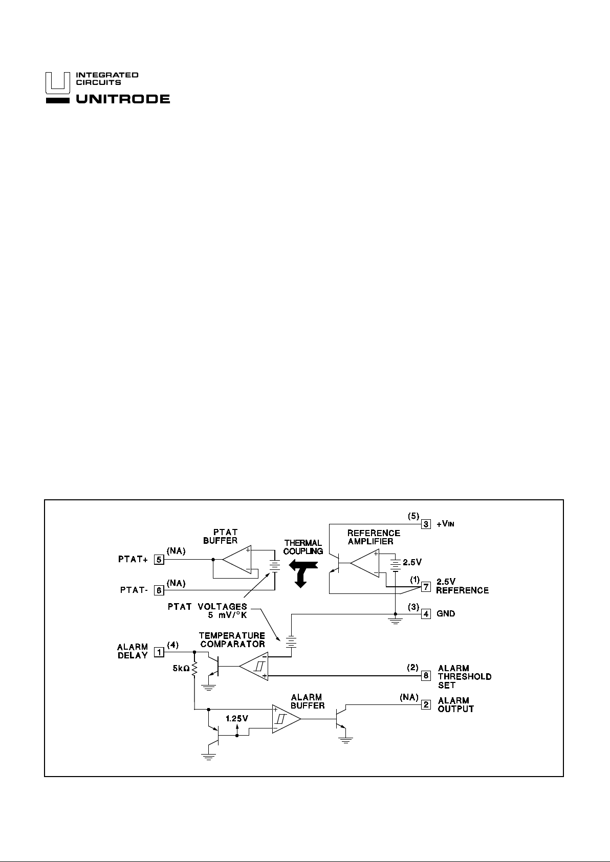
The UC1730 family of integrated circuit devices are designed to be used in
a number of thermal monitoring applications. Each IC combines a temperature transducer, precision reference, and temperature comparator allowing
the device to respond with a logic output if temperatures exceed a user programmed level. The refe rence on these devices is capable of supplying in
excess of 250mA of output current − by setting a l evel o f power dissipation
the rise in die temperature will vary with airflow past the package, allowing
the IC to respond to airflow conditions
These devices come in an 8-Pin DIP, plastic or ceramic, a 5-Pin TO-220 or a
PLCC-20 version. In the 8-Pin version, a PTAT (proportional to absolute
temperature) output reports die tempe rature directly. This output is configured such that its output level can be easily scaled up with two external gain
resistors. A second PTAT source is internal ly refere nced to the temperature
comparator. The other input to this comparator can then be externally programmed to set a temperature threshold. When this temperature threshold
is exceeded an alarm delay output is activated. Following the activation of
the delay output, a separa te open colle ctor output is turn ed on. The delay
pin can be programmed with an external RC to provide a time separation
between activation of the del ay pin and the alarm pin, p ermitting shutdown
diagnostics in applications where the open collector outputs of multiple parts
are wire OR’ed together .
The 5-Pin version in the TO-220 package is well suited for monitoring
heatsink temperatures. Enha nced airfl ow sensiti vities can be obtained with
this package by mou nting the device to a small heatsink in the airstream.
This version of the device does not include the PTAT output or the open collector alarm output.
FEATURES
• On-Chip Temperature Trans ducer
• Temperature Comparator Gives
Threshold Temperature Alarm
• Power Reference Permits Airflow
Diagnostics
• Precision 2.5V Power Reference
Permits Airflow Diagnostics
• Transducer Output is Easily Scaled
for Increased Sensitivity
• Low 2.5mA Quiescent Current
BLOCK DIAGRAM
10/94
Pin numbers shown for 8-Pin DIP, ( ) number for 5-Pin TO-22 0.
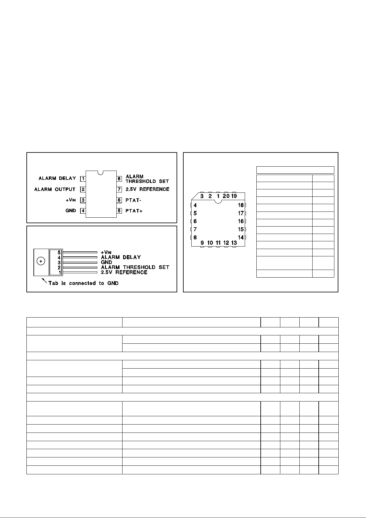
PACKAGE PIN FUNCTION
FUNCTION PIN
N/C 1-3
ALARM DELAY 4
ALARM OUTPUT 5
+V
IN 6
GND 7
N/C 8-13
PTAT+ 14
PTAT- 15
2.5V REFERENCE 16
2.5V REFERENCE 17
ALARM
THRESHOLD SET
18
N/C 19-20
Input Supply Voltage, (+VIN). . . . . . . . . . . . . . . . . . . . . . . 40V
Alarm Output Voltag e (8-Pin Vers ion Only). . . . . . . . . . . 40V
Alarm Delay Voltage. . . . . . . . . . . . . . . . . . . . . . . . . . . . . 10V
Alarm Threshold Set Voltage . . . . . . . . . . . . . . . . . . . . . . 10V
2.5V Reference Output Current . . . . . . . . . . . . . . . . . -400 mA
Alarm Output Current (8-Pin Vers io n Only) . . . . . . . . . . 0 mA
Power Dissipation at T
A = 25 °C (N ote 2) . . . . . . . . . 1000 mW
Power Dissipation at T
C = 25°C (Note 2). . . . . . . . . 200 0 m W
Therma l Resis ta nce Ju nct ion to Amb ie nt
N, 8-Pin Plastic DI P . . . . . . . . . . . . . . . . . . . . . . . . . 110°C/W
J, 8-Pin Ceramic DIP . . . . . . . . . . . . . . . . . . . . . . . . 110°C/W
T, 5-Pin Plastic DIP TO- 220 . . . . . . . . . . . . . . . . . . . . 65°C/W
Thermal Resis tance Ju nct ion to Case
N, 8-Pin Plastic DI P. . . . . . . . . . . . . . . . . . . . . . . . . . . 60°C/W
J, 8-Pin Ceramic DIP. . . . . . . . . . . . . . . . . . . . . . . . . . 40°C/W
T, 5-Pin Plastic TO -22 0. . . . . . . . . . . . . . . . . . . . . . . . . 5°C/W
Operating Junct ion Te mp era tu re . . . . . . . . . -55°C to +150°C
Storage Temperature . . . . . . . . . . . . . . . . . . -65°C to +150°C
Lead Tempera tu re (Solderin g, 10 Seconds). . . . . . . . . 300°C
Note 1: Voltage s are refer ence d to grou nd. Current s are positive into, negative out of, the specified terminals.
Note 2: Consult Packaging sectio n of Data book for therma l
limitations and con sider atio ns of pack age.
DIL-8 (TOP VIEW)
N or J Package
5-PIN TO-220 (TOP VIEW)
T Package
UC1730
UC2730
UC3730
CONNECTION DIAGRAMS
PLCC-20 (TOP VIEW)
Q Package
ABSOLUTE MAXI MUM RATING S
ELECTRICAL CHARACTERISTICS:
PARAMETERS TEST CONDITIONS MIN TYP MAX UNITS
INPUT SUPPLY
Supply Current +V
IN = 35V 2.8 4.0 mA
+V
IN = 5V 2.3 3.5 mA
REFERENCE
Output Volt age TJ = 25°C 2.475 2.5 2.525 V
Over Temperature 2.46 2.54 V
Load Regulation I
OUT = 0 to 250mA 8.0 25 mV
Line Regulation +V
IN = 5 to 25V 1.0 5.0 mV
TEMPERATURE COMPARATOR
Temperature Com par ator Thre shold at 300°K (26.85°C), Nominally 5m V/ °K,
V
INPUT High to Low
1.475 1.50 1.525 V
Tempe rat ure Error -10 10 °C
Threshold Line Regula tion +V
IN = 5 to 25V 0.005 0 .0 2 %/V
Temperature Linearit y Note 2 2.0 5.0 °C
Threshold Hyster esis 3.0 8.0 15 mV
Input Bias Cur ren t V
INPUT at 1.5V -0.5 -0.1 µA
Max Output Current VOUT = 1V 1.2 3.0 mA
Output Sat Volta ge I
OUT = 100µA 0.05 0.25 V
Unless otherw ise stat ed, these sp ecif icat io ns apply for TJ = 0°C to +100°C f or the
UC3730, -25°C to + 100°C for the UC2730 and -55°C to +125°C for the UC1730,
+VIN = + 5V, and PTAT– = 0V. TA = TJ.
2

ELECTRICAL
CHARACTERISTICS (con t):
PARAMETERS TEST CONDITIONS MIN TYP MAX UNIT
TEMPERATURE COMPARATOR (cont .)
Output Lea kage Current V
OUT = 1V 0.01 1.0 µA
PTAT BUFFER (8-Pin N, or J Version Only)
Output Voltage at 300°K (26.85°C), Nominally 5mV/ ° K 1.460 1.50 1.54 V
In 10X Config. + V
IN = 25V 14.6 15 15.4 V
Tempe rat ure Error -12 12 °C
Temperature Linea rity (Not e 2) 2.0 5.0 °C
Line Regulation +V
IN = 5 to 25V 0.02 0.04 %/V
Load Regulation I
OUT = 0 to 2mA 1. 0 3.0 mV
Dropout Voltage PTAT + TO +VIN 1.9 2.5 V
Input Bias Current at PTAT– Input -3.0 -1.0 µA
ALARM BUFFER COMPARATOR (8-Pin N, or J Version Only)
Threshold Voltage (V
TH) Alarm Delay Input Low to High 1.1 1.2 1.3 V
Threshold Hyster esis Volt age Alarm Delay Voltage > VTH 100 250 mV
Input Bias Curren t Alarm Delay Voltage < V TH 0. 1 0.5 µA
Max Output Current V
OUT = 1V 7.0 15 mA
Output Sat Volta ge IOUT = 3mA 0.25 0.45 V
Output Lea kage V
OUT = 35V 0.1 2.0 µA
UC1730
UC2730
UC3730
Unless otherwise stated , thes e specificat ions apply for TJ = 0°C to +100°C for the UC3730,
-25°C to + 100°C for the UC2730 and -55°C to +125°C for the UC1730 , +V
IN = + 5V, a nd
PTAT– = 0V. T
A = TJ.
Note 2: This parameter is guara nt eed by design an d is not tes ted in product ion.
APPLICATIONS AND OPERATION INFORMATION
V
OUT
= 5 x
1
+
R2
R1
mV
⁄
°
K
(Recommended Range for R1 is 2k to 4k)
Scaling the PTAT Output (8 Pin Version Only)
VREF Maximum Output Current vs Input Supply Ju n cti on Temperature Rise vs Airflow UC3730N (8-
Pin Plastic Dip)
3

Tempe ratur e Threshold (°C)
=
(
2.5V
0.00 5
)
x
R2
R1
+
R2
− 273.15
Note:For airflow monitoring a power dissipation
level can be set with a resistive load, R
L
, on the
reference output. P
D
= (+ V
IN
- 2.5V)2/RL.
APPLICATIONS AND OPERATION INFORMATION (Cont.)
UC1730
UC2730
UC3730
Setting a Temperature Th resho ld
Dual Speed Fan Control
TH(°C) =
2.5V
0.005
x
R2
R1+R2
−
273.15
TL(°C) =
2.5V
0.005
x
R
X
R1+R
X
−
273.15
Where: RX = R2
×
R3
R2
+
R3
UNITRODE INTEGRATED CIRCUITS
7 CONTINENTAL BLVD. •• MERRIMACK, NH 03054
TEL. (603) 424-2410 •• FAX (603) 424-3460
4

IMPORTANT NOTICE
T exas Instruments and its subsidiaries (TI) reserve the right to make changes to their products or to discontinue
any product or service without notice, and advise customers to obtain the latest version of relevant information
to verify, before placing orders, that information being relied on is current and complete. All products are sold
subject to the terms and conditions of sale supplied at the time of order acknowledgement, including those
pertaining to warranty, patent infringement, and limitation of liability.
TI warrants performance of its semiconductor products to the specifications applicable at the time of sale in
accordance with TI’s standard warranty. Testing and other quality control techniques are utilized to the extent
TI deems necessary to support this warranty. Specific testing of all parameters of each device is not necessarily
performed, except those mandated by government requirements.
CERT AIN APPLICATIONS USING SEMICONDUCTOR PRODUCTS MAY INVOLVE POTENTIAL RISKS OF
DEATH, PERSONAL INJURY, OR SEVERE PROPERTY OR ENVIRONMENTAL DAMAGE (“CRITICAL
APPLICATIONS”). TI SEMICONDUCTOR PRODUCTS ARE NOT DESIGNED, AUTHORIZED, OR
WARRANTED TO BE SUITABLE FOR USE IN LIFE-SUPPORT DEVICES OR SYSTEMS OR OTHER
CRITICAL APPLICATIONS. INCLUSION OF TI PRODUCTS IN SUCH APPLICA TIONS IS UNDERSTOOD T O
BE FULLY AT THE CUSTOMER’S RISK.
In order to minimize risks associated with the customer’s applications, adequate design and operating
safeguards must be provided by the customer to minimize inherent or procedural hazards.
TI assumes no liability for applications assistance or customer product design. TI does not warrant or represent
that any license, either express or implied, is granted under any patent right, copyright, mask work right, or other
intellectual property right of TI covering or relating to any combination, machine, or process in which such
semiconductor products or services might be or are used. TI’s publication of information regarding any third
party’s products or services does not constitute TI’s approval, warranty or endorsement thereof.
Copyright 1999, Texas Instruments Incorporated
 Loading...