

Datasheet UC3726DWPTR, UC3726DWP, UC3726N, UC2726N, UC2726DWPTR Datasheet (Texas Instruments)
...
• 750mA Output Drive, Source or Sink
• 8 to 35V Operation
• Transmits Drive Logic and Power
through Low Cost Transformer
• Programmable Operating Frequency
• Up to 750kHz Operation
• Improved Output Control Algorithm
Minimizes Output Jitter
• Fault Logic Monitors Isolated High
Side IGBT Driver UC1727 for Faults
• User Programmable Fault Timing
Screens False Fault Signals
• Shutdown Mode Disables On Chip
Logic Reference for Low Standby
Power
• Optional External Biasing of Logic
Circuitry can Reduce Overall Power
Dissipation
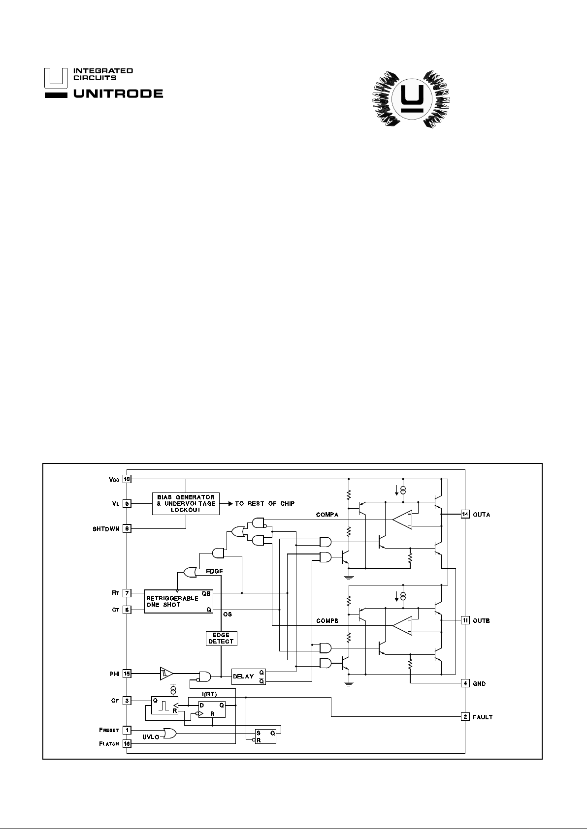
The UC1726 Isolated Drive Transmitter, and its companion chip, the
UC1727 Isolated High Side IGBT Driver, provide a unique solution to driving isolated power IGBTs. They are particularly suited to drive the high
side device s on a high voltage H-bridge. The UC1726 device transmits
the drive logic and drive power, along with transferring and receiving fault
information with the isolated gate circuit using a low cost pulse transformer.
This drive system utilizes a duty cycle modulation technique that gives instantaneous response to the drive control transitions, and reliably passes
steady state, or DC conditions. High frequency operation, up to 750kHz,
allows the cost and size of the coupling transformer to be minimized.
The UC1726 can be powered from a single V
CC supply whi ch internally
generates a voltage reference for the logic circuitry. It can also be placed
into a low power shutdown mode that disables the internal reference. The
IC’s logic ci rcuitry can b e powered from an external suppl y, V
L, to mini-
mize overall power dissipation. Fault logic monitors the Isolated High Side
IGBT Driver UC1727 for faults. Based on user defined timing, the
UC1726 distinguishes valid faults, which it responds to by setting the fault
latch pin. This also disables the gate drive information until the fault reset
pin is toggled to a logic one.
The UC1726 opera te s ove r an 8 to 3 5 vo lt su ppl y range. The typical V
CC
voltage will be greater than 28 volts t o be compatible with the UC1727.
The undervoltage lockout circuitry of the Isolated High Side IGBT Driver
UC1727 locks out the drive information during its under voltage lockout.
Isolated Drive Transmitter
FEATURES
DESCRIPTION
BLOCK DIAGRA M
UC1726
UC2726
UC3726
7/95
UDG-94004-1
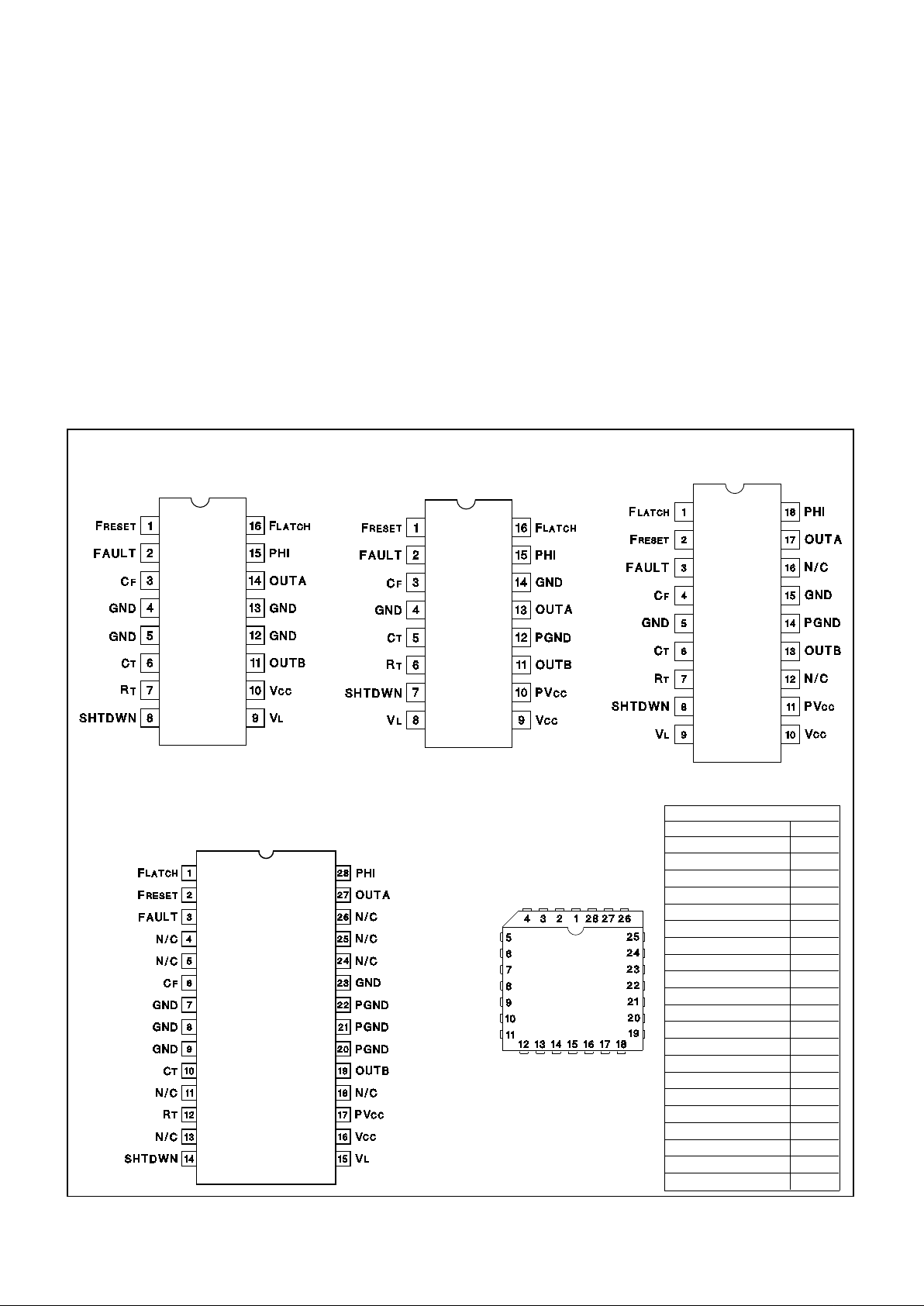
CONNECTION DIAGRAMS
UC1726
UC2726
UC3726
ABSOLUTE MAXI MUM RATING S
Supply Voltage VCC . . . . . . . . . . . . . . . . . . . . . . . . . . . . . 40 V
Source/ Sink Current (Pulsed). . . . . . . . . . . . . . . . . . . . . . 1.5A
Source/ S in k Curr ent (Continuous) . . . . . . . . . . . . . . . . . . 1.0A
Output Voltag e (pins 12, 14). . . . . . . . . . −0.3 to (V
CC + 0.3)V
C
F, FRESET, FAULT, SHTDWN,
F
LATCH, VL, PHI, RT . . . . . . . . . . . . . . . . . . . . . . . −0.3 to 6. 0V
C
T . . . . . . . . . . . . . . . . . . . . . . . . . . . . . . . . . . . . . . 1.0 to 6.0V
Operating Junct ion Te mp era tu re (Not e 2) . . . . . . . . . . 150°C
Storage Temperature Range . . . . . . . . . . . . . −65°C to 150°C
Lead Temp era ture (Solder in g, 10 seconds). . . . . . . . . 300 °C
Note 1: All voltages are with res pect to GND ( Pin 2); all
currents are posit ive int o, negat ive ou t of part .
Input Voltage. . . . . . . . . . . . . . . . . . . . . . . . . . . . . . . +9 to +35.0V
Sink/Source Curre nt (each out put ). . . . . . . . . . . . . . . 0 to 750mA
Timing Resistor. . . . . . . . . . . . . . . . . . . . . . . . . . . . 2.4k to 200kΩ
Timing Capacitor (C
T). . . . . . . . . . . . . . . . . . . . . . . 75pF to 2.0nF
Timing Capacitor (C
F). . . . . . . . . . . . . . . . . . . . . . . 75pF to 3.0nF
Note 2: See Unitrod e Inte gra ted C ircuit s datab ook f or inform at ion
regarding thermal spe cifica tion s and limit ations of
packages.
Note 3: Range over which the device is functional and par amet er
limits are guaranteed.
RECOMMENDED OPERATING CONDITIONS (Note 3)
DIL-16 (Top View)
N Package
DIL-16 (Top View)
SP Package
DIL-18 (Top View)
J Package
SOIC-28 (Top View)
DWP Package
PACKAGE PIN FUNCTION
FUNCTION PIN
GND 1
C
T 2
N/C 3-4
R
T 5
SHTDWN 6
V
L 7
V
CC 8
N/C 9
PV
CC 10
OUTB 11
PGND 12-18
GND 19
OUTA 20
PHI 21
F
LATCH 22
F
RESET 23
FAULT 24
N/C 2 5
C
F 26
N/C 2 7
N/C 2 8
PLCC-28 (Top View)
QP Package
2

UC1726
UC2726
UC3726
PARAMETERS TEST CONDITIONS MIN TYP MAX UNITS
Retriggerable one shot
Initial Accuracy T
J = 25°C 1.400 1.600 1.800 µsec
Temperature Stability Over operating TJ 1.000 2.200 µsec
Voltage Stability V
CC = 10 to 35V 0.2 %/V
Operating Freque ncy L
LOAD = 1.5mH 170 kHz
PHI Input (Control Input)
HIGH Input Voltage 2.0 V
LOW Input Voltage 0.8 V
HIGH Input Current 10 µA
LOW Input Current -300 −60 0 µA
Delay to one shot 100 250 nsec
Delay to Output C
T = 1.4V 250 nsec
Output Drivers
Output Low Le vel I
SINK = 20mA 0.3 0.5 V
I
SINK = 400mA 0.5 2.6 V
Output High Level I
SOURCE = −20mA 2.0 2.6 V
(volts below V
CC)ISOURCE = −400mA 2.0 2.9 V
Rise and Fall Times No load 30 60 nsec
Logic Voltage Reference
V
L - Logic Voltage Internal Voltage 4.20 4 .4 0 4.60 V
Logic Supply Current V
L = 4.75V to 5.25V, CT = 1.4V 13.0 20.0 mA
Shut Down Circuit
Logic Voltage - Off 0.5 V
High Input Current V
IH = 2.4 -100 µA
Low Input Current V
IL = 0.4 -20 µA
Fault Logic
Fault Reset High Input Current V
IH = 2.4
±
5 µA
Fault Reset Low Input Current V
IL = 0.4 -10 µA
Fault High Input Cur rent V
IH = 2.4
±
5 µA
Fault Low Input Current V
IL = 0.4 -60 µA
Fault Pulse Width C
F = 330pF 3.0 µs
C
F = 2.2nF 17.0 µs
Fault Latch, V
OH ILOAD = −1mA, Volts below VL 1.3 1.8 V
Fault Latch, V
OL ILOAD = 1mA 0.25 0.5 V
Fault Latch, VOH ILOAD = 0, Volts below VL 0.3 V
Fault Latch, V
OL ILOAD = 0 0.2 V
Fault Reset Pulse Width 500 ns
UVLO
Turn On Thresho ld 7.1 V
Total Supply Current
Supply Current C
T = 1.4V 22 40 mA
C
T = 1.4V, VL = 5.0V 12 20 mA
CT = 1.4V, Shutdown = 5.0V 2.5 mA
Unless otherwise stated, VCC = 20V, RT = 4.32kΩ, CT = 330pF and CF = 2.2nF, no
load on any output, and −55°C < T A < 1 25°C for the UC1726, −40°C < TA < 85°C for
the UC2726, and 0°C < TA < 70°C for the UC3726, TA = T J.
ELECTRICAL CHARACTERISTICS:
3

UC1726
UC2726
UC3726
PIN DESCRIP TI ONS
CF: The timing input to the fault logic. A capacitor is
placed across the input of C
F and ground. The timing win-
dow is approximately t = 2.1C
FRT.
C
T: The connection to the timing capacitor that controls
the operating frequ ency. A capacitor to ground is repetitively charg ed during the one sh ot pulse width. It is discharged when a comparator senses zero current in the
primary side of the transformer. The one shot pulse width
is consequently determined by the time it takes to charge
the capacitor from a threshold voltage of V
L/4 to VL/2.
This pin must be tied t o a capacitor. See Recommended
Operating Conditions.
FAULT: This input t o the faul t logi c i nitiates th e user programmable timer. This time interval, specified by the capacitor on C
F, determines the validity of the fault. The pin
is tied to a low cost optocoupler, and is high until the
UC1727 sends drive information from the PHI pin through
the transformer while the FAULT pin stays low. Once this
pin goes high, it must stay high during the entire fault window to be a ccepted as a va li d fault. A valid fault sets the
F
LATCH pin high and prevents the transmitting of gate
drive information until the F
RESET is toggled high. If fault
logic is not used, the FAULT pin must be grounded.
F
LATCH: A valid fault sets this pin to a logic one and pre-
vents the transmitting of gate drive information. The
F
LATCH pin can only be reset by connecting the FRESET to
a logic 0.
F
RESET: The input to the fault logic that resets the fault
logic latch (F
LATCH) and enables drive transmit data. This
input must be low when powered up and stay low until after the fault latch has been set.
GND: The signal and power ground for the device. The
power ground of the output transistor is isolated on the
chip from the subs trate groun d which biases the remainder of the device.
OUTA: One output of the two totem pole outputs connected across the transformer primary winding. When
PHI is high, the output toggles between 0.3V during the
one shot charge time and approximately V
CC + 0.4V dur-
ing the remainder of the period. When PHI is low the output toggles between V
CC - 2V during the one shot charge
time and approximately 0.6V
CC during the remainder of
the period.
OUTB: One output of the two totem pole outputs connected across the transformer primary winding. When
PHI is high, the output toggl es between V
CC - 2V during
the one shot charge time and approximately 0.6V
CC dur-
ing the remainder of the period. When PHI is low the output toggles between 0.3V during the one shot charge
time and approximately V
CC + 0.4V during the remainder
of the period.
PGND: This is the ground for the output transistors
bonded i n the 28 pin packag es. On the six teen pin packages it is bonded separately to the GND pin.
PHI: A logic control input to the isolated gate drive that
changes the outputs as described above. This changes
the duty cycle of the voltage wave form applied across
the transformer. The Isolated High Side IGBT Driver
UC1727 senses the different duty cycles as different
drive commands.
PV
CC: This is the input vol tage for the output transistors
on the 28 pin package. On the sixteen pin packages it is
bonded separately to the V
CC pin.
R
T: The input that sets the CT and CF capacitor currents
with a resistor to ground . The voltage on R
T is approxi-
mately 0.3V
L. The resulting charge currents are: ICT =
IC
F = VL / 4RT.
SHTDWN: This input shuts down the internal reference. A
TTL logic one puts the UC1726 into a low standby current
mode. This input has a pull down resistor on the chip to
guarantee proper operation when left open. If an external
logic voltage i s applied to V
L, this shutdown feature can-
not be used without bringi ng the external voltage source
to zero volts.
V
CC: The input voltage that biases the outputs and the in-
ternal reference. It can vary between 8V to 35V. This supply pin will typically be greater than 28V to be compatible
with the UC1727. In order to min imize pow er dissipation
use an external logic supply, V
CC approximately 15V, and
a step up transformer (N = 2).
V
L: The logic supply pin that biases all circuits except for
the totem pole outputs. A bypass capacitor is recommended on thi s pin when lef t unconnected. The internal
reference is approximately 4.4V. A 5.0V supply can be
applied to thi s pin to assure minimum power dissipation.
When an external supply higher than the V
L voltage is
applied to this pin, the internal reference turns off.
Refer to Typical Appli cati on on Page 5 and Applicatio n Note U- 143A "New Ch ip Pair Provi des Iso l ated Drive
for High Voltage IGBTs"
4

UC1726
UC2726
UC3726
TYPICAL APPLICATIO N
UNITRODE INTEGRATED CIRCUITS
7 CONTINENTAL BLVD. • • MERRIMACK, NH 03054
TEL. (603) 424-2410 •• FAX (603) 424-3460
IF FAULT LOGIC NOT USED, GROUND FAULT PIN.
UDG-94006
The chip operating frequency is determined by the values
of components connected to the R
T and CT pins. A resis-
tor connected between R
T and ground sets the charge
current to IC
T = VL / 4RT. The operating frequency varies
slightly depending on the V
CC and VL voltages. The fol-
lowing equations approximate the one shot pulse width at
operating frequency when V
CC = 20V.
T
PW = 1.1RT(CT + 50pF)
F
O
=
1
3.3
R
T
(
C
T
+ 50pF)
The 50pF additional capacity represents internal chip capacitance at the C
T input.
OPERATING FREQ UENCY :
5

IMPORTANT NOTICE
T exas Instruments and its subsidiaries (TI) reserve the right to make changes to their products or to discontinue
any product or service without notice, and advise customers to obtain the latest version of relevant information
to verify, before placing orders, that information being relied on is current and complete. All products are sold
subject to the terms and conditions of sale supplied at the time of order acknowledgement, including those
pertaining to warranty, patent infringement, and limitation of liability.
TI warrants performance of its semiconductor products to the specifications applicable at the time of sale in
accordance with TI’s standard warranty. Testing and other quality control techniques are utilized to the extent
TI deems necessary to support this warranty. Specific testing of all parameters of each device is not necessarily
performed, except those mandated by government requirements.
CERT AIN APPLICATIONS USING SEMICONDUCTOR PRODUCTS MAY INVOLVE POTENTIAL RISKS OF
DEATH, PERSONAL INJURY, OR SEVERE PROPERTY OR ENVIRONMENTAL DAMAGE (“CRITICAL
APPLICATIONS”). TI SEMICONDUCTOR PRODUCTS ARE NOT DESIGNED, AUTHORIZED, OR
WARRANTED TO BE SUITABLE FOR USE IN LIFE-SUPPORT DEVICES OR SYSTEMS OR OTHER
CRITICAL APPLICATIONS. INCLUSION OF TI PRODUCTS IN SUCH APPLICA TIONS IS UNDERSTOOD T O
BE FULLY AT THE CUSTOMER’S RISK.
In order to minimize risks associated with the customer’s applications, adequate design and operating
safeguards must be provided by the customer to minimize inherent or procedural hazards.
TI assumes no liability for applications assistance or customer product design. TI does not warrant or represent
that any license, either express or implied, is granted under any patent right, copyright, mask work right, or other
intellectual property right of TI covering or relating to any combination, machine, or process in which such
semiconductor products or services might be or are used. TI’s publication of information regarding any third
party’s products or services does not constitute TI’s approval, warranty or endorsement thereof.
Copyright 1999, Texas Instruments Incorporated
 Loading...