

UC1702
UC2702
UC3702
DESCRIPTION
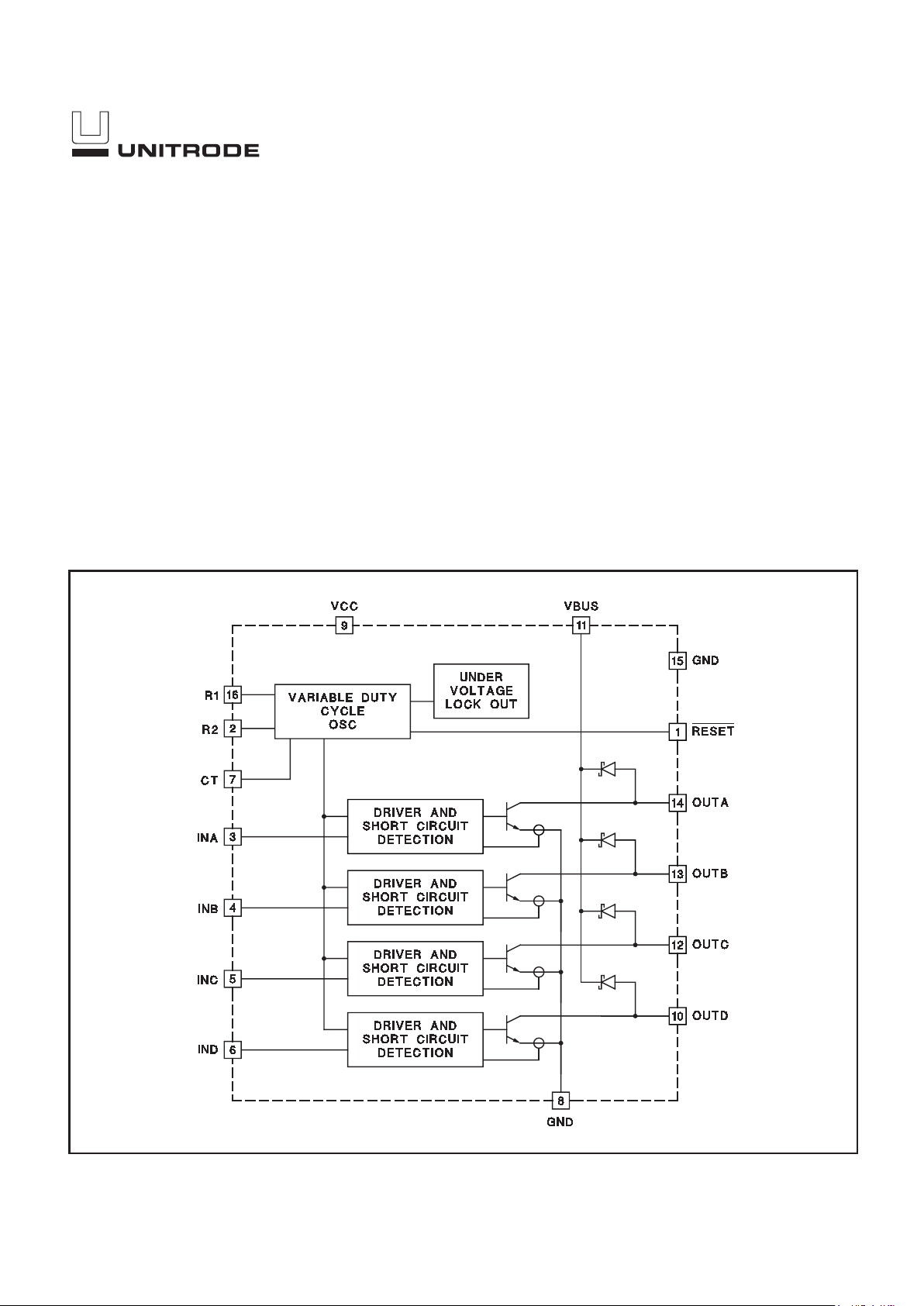
The UC3702 Quad Relay Driver is intended to drive up to four relays from
logic inputs using an unregulated relay voltage supply. The relays are
driven from the Bus supply in a power efficient PWM converter fashion.
The relay coil is used as the inductive element. (See the application's sec
tion concerning the relay selection.) VBUS must be higher then the rated
relay voltage. Short circuit protection is provided on chip with periodic retry.
The UC3702 requires a +5V logic supply as a reference. Two external re
sistors program the effective relay voltage and a capacitor sets the nominal
operating frequency. Internal Schottky diodes eliminate the need for any
external power components.
In typical applications, the UC3702 grants the user the flexibility to choose
the most cost effective relay without the added burden of generating a sep
arate relay supply voltage. The UC3702 will even function with a poorly
regulated supply VBUS, containing significant 100Hz or 120Hz ripple.
Quad PWM Relay Driver
FEATURES
•
Maintains Constant Average
Relay Voltage With Varying
Supply Voltages
•
VBUS Voltages up to 42.5V
•
Up to 50mA per Relay
•
Integrated Schottky Flyback Diodes
•
Individual Relay Control Inputs
•
Short Circuit Protection
•
User Selectable Operating Center
Frequency and Relay Voltage
•
Global Reset
SLUS368 - APRIL 1997
BLOCK DIAGRAM
UDG-96009-1
2
UC1702
UC2702
UC3702
ABSOLUTE MAXIMUM RATINGS
VBUS. . . . . . . . . . . . . . . . . . . . . . . . . . . . . . . . . . . . . . . . . +50V
VCC. . . . . . . . . . . . . . . . . . . . . . . . . . . . . . . . . . . . . . . . . . . +9V
Input Voltage . . . . . . . . . . . . . . . . . . . . . . –0.3V to VCC + 0.3V
Average Current per Relay. . . . . . . . . . . . . . . . . . . . . . . . 50mA
Total Output Capacitance. . . . . . . . . . . . . . . . . . . . . . . . . 25pF
Storage Temperature . . . . . . . . . . . . . . . . . . . –65°C to +150°C
Junction Temperature. . . . . . . . . . . . . . . . . . . –55°C to +150°C
Lead Temperature (Soldering, 10 sec.) . . . . . . . . . . . . . +300°C
Currents are positive into, negative out of the specified termi
-
nal. Consult Packaging Section of Databook for thermal limita
-
tions and considerations of packages.
ELECTRICAL CHARACTERISTICS: Unless otherwise stated these specifications apply for T
A
= –55°C to +125°C for
UC1702; –25°C to +85°C for UC2702; 0°C to +70°C for UC3702; VBUS = 34V, VCC = 5V, RESET
= VCC, R2 = 43.2k ;
R1 = 203k
; CT = 220pF, TA= TJ.
PARAMETER
TEST CONDITIONS MIN TYP MAX UNITS
Supply Voltage Section
VCC 4.5 5 8 V
VCC Supply Current RESET
, INA, INB, INC, IND = VCC 4 6 mA
VBUS 42.5 V
Oscillator Section
NOMINAL Operating Frequency R1 = 203k
, R2 = 43.2k , CT = 220pF 150 175 200 kHz
R1 100 202 500 k
R2 20 42.5 80 k
CT 100 pF
Output Driver VBUS = 20V
Rated Relay Current 50 mA
Short Circuit Current 100 175 mA
Diode Leakage Current Control Input Low, V
OUTX
= VBUS 0.05 5 A
Diode Forward Voltage 500 mV
Averaged Output Voltage Error UC2702, UC3702 (Note 1) –10 10 %
UC1702 –20 20 %
Control Inputs (INA, INB, INC, IND)
Logic Low 0.5 V
Logic High 3 VCC V
TON / TOFF Delay 250 ns
Input Current –1 0 1
A
Input Current V
IN
= 5V 70 120 A
RESET
TON / TOFF Delay 2 s
Input Current V
IN
= 0.3V –8 –5 A
Input Current V
IN
= 5V –10 0 10 A
Note 1: Programmed Average Voltage
=
••
•
106 1
22
400
.
–
RVCC
R
mV
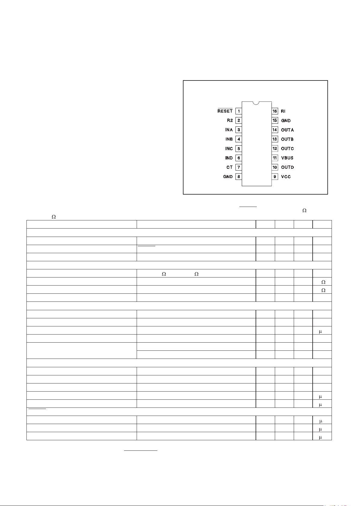
CONNECTION DIAGRAM
DIL-16, SOIC-16 (Top View)
J or N, D Package

3
UC1702
UC2702
UC3702
CT: A capacitor from the CT pin to ground sets the oscil
lator center frequency. Note that the oscillator period
must be least an order of magnitude less than the relax
ation time constant (L/R) of the relay coil. However, a
needlessly high operating frequency only increases
power dissipation. For best accuracy, CT should be
220pF or greater.
GND: Both ground pins must be connected to a low
noise system ground.
INA, INB, INC, IND: Separate digital control inputs for
each of the four relay drivers. An active high input (a
logic high) turns on the respective relay. Active low dis
ables the common-emitter drive transistor.
OUTA, OUTB, OUTC, OUTD: Each of these output pins
can be connected to the low side of one relay coil. The
rated relay coil voltage of all relays to be driven by a sin
gle UC3702 must be the same. (It is permissible to use
coils with different rated series resistances with a single
UC3702, so long as the rated coil voltages are the same
and care is taken with respect to the relaxation times of
the different relay coils). Output transients are slew rate
limited to decrease electro-magnetic radiation.
R1: User selected external resistor must be placed from
the R1 pin to the VBUS voltage supply. Sensing the
VBUS amplitude, the oscillator varies its ON duty cycle
such that the average voltage across the driver coil is
constant.
R2: User selected external resistor must placed from R2
pin to GND. This resistor, in conjunction with the external
timing capacitor, CT, sets the OFF cycle time of the oscil
-
lator. For best accuracy, use 42.3kΩ for R2.
RESET:
Digital reset pin is active low. When RESET is
low, the oscillator stops running and all drivers are open
collector.
VCC: Nominally 5V. In addition to supplying the voltage
for the driver logic and oscillator circuit, the VCC supply
is used as reference for the generating the average relay
voltage. It is recommended that the VCC be regulated to
±5% of its nominal value or better to insure good regula
-
tion. Good decoupling with a minimum of 1µF is neces
-
sary.
VBUS: This pin should be tied to a low impedance voltage source at some voltage higher than the rated voltage
of the relay coil to be driven. VBUS may even be a
poorly filtered rectified sin wave, as the UC3702 will regulate the correct duty cycle. Good decoupling with a minimum of 1µF is necessary.
PIN DESCRIPTIONS
The UC3702 must be programmed for a specific relay
voltage. The table given below has some suggested val
-
ues of R1, R2, and CT. The VCC supply voltage is as
-
sumed to be 5V.
More generally, the following equation can be used to
determine the equivalent average relay voltage:
V
VCC R
R
mV
RELAY
=
••
•
106 1
22
400
.
–
Industrial Relays
The UC3702 takes advantage of the inductance of the
relay coil to regulate a constant coil current in a manner
very similar to a switch-mode power supply. To use the
UC3702 correctly, the coil characteristics must be
known. The rated relay voltage is what the relay manu
facturers specify as voltage to drive the relay coil with if
the coil were driven from a dc source. Most manufactur
ers also specify the series resistance of the coil. This is
the resistance of the copper wire and determines the
steady state coil ON current. For example, a 12V relay
with a 320
series coil resistance with a draw of 37.5mA
of constant current. The relay inductance is not typically
specified in the manufacturer’s short-form datasheet, so
the engineer will need an LCR bridge to measure it or re
-
quest the information from the relay manufacturer.
APPLICATIONS INFORMATION
Rated Relay
Voltage
R1 R2 CT
9V 153kΩ 43.2kΩ 220pF
12V 203kΩ 43.2kΩ 220pF
24V 398kΩ 43.2kΩ 220pF

4
UC1702
UC2702
UC3702
Although the inductance may not be specified in the re
lay datasheet, it is very repeatable since it is determined
by the number of turns and geometry of the relay.
The relay’s coil inductance divided by its series resis
tance is the relay coil’s relaxation time constant. It is im
portant that the relaxation time constant be at least an
order of magnitude longer than the nominal switching pe
riod of the UC3702 to obtain a constant current through
the relay coil. This means that some relays may be
ill-suited for use with the UC3702.
For example, a common 12V industrial relay has a series
resistance of 500
and a coil inductance of 500mH. Its
relaxation time constant is 1ms, an order of magnitude
less than the period of a 10kHz oscillator.
When performing an engineering evaluation of the
UC3702 in a system, it is useful to have a current probe.
Alternately, a 1
resistor can be placed in series with the
relay coil in the prototype and differential voltage probes
can be used to observe the coil current. (Do not use a
large series resistor, as this will impact observed relax
-
ation time constant.)
Layout Considerations
The layout of the printed circuit board and good decoup
ling of the power supplies is critical to proper operation of
the UC3702. For best results, high quality 4.7
F tanta
lum capacitors should be placed as close as possible to
the VCC and the VBUS pins.
In addition to decoupling considerations, the R1 and R2
pins are sensitive to capacitive coupling from any of the
driver outputs (OUTA - D) which can slew at speeds of
300V/
s. The external resistors R1 and R2 should be
placed as close as possible to their respective pins.
Avoid routing the outputs directly past these pins without
a low impedance trace (such as GND, VCC, or VBUS) in
between to act as a capacitive shield.
APPLICATIONS INFORMATION (cont.)
Typical Microcontroller Application Driving 12V Industrial Relays
UNITRODE CORPORATION
7 CONTINENTAL BLVD. • MERRIMACK, NH 03054
TEL. (603) 424-2410 • FAX (603) 424-3460
UDG-96010-1
 Loading...