

UC2578
UC3578
05/99
FEATURES
• Provides Simple Single Inductor Buck
PWM Step-Down Voltage Regulation
• Drives External High Side NMOS
Switch
• 14V to 72V Input Voltage Operating
Range
• Contains 100kHz Internal Oscillator,
2V Reference and UVLO
• Soft Start on Power Up
• Overcurrent Shutdown Followed by
Soft Start
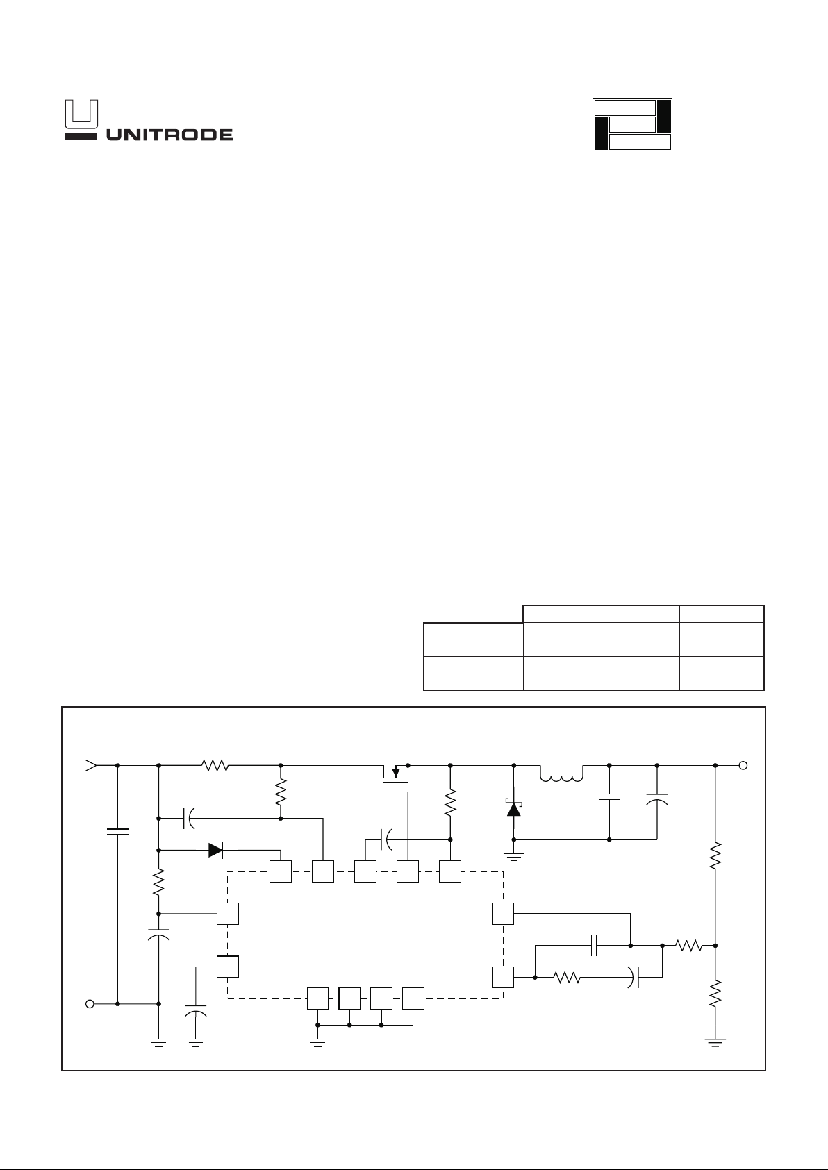
Buck Pulse Width Modulator Stepdown Voltage Regulator
14
16
11 15 10 7 6
2
3
131254
EAINV
EAOUTGNDGND
SRCOUT
SS
CS
VCC
GND GND
DIODE VGG
UC3578
C
SS
2200pF
100k
220pF
50k
R1
1k
5k
C
GG
1µF
15
C
CC
1µF
47µF
10
1N4148
C
S
1000pF
R
S
1k
R
SENSE
0.12
IRFZ34
15-40 V
IN
1µF
C
OUT
220µF
L
OUT
40µH
RECTIFIER
MBR 3100
V
OUT
TYPICAL APPLICATION DIAGRAM
UDG-99064
DESCRIPTION
The UC3578 is a PWM controller with an integrated high side floating gate
driver. It is used in buck step down converters and regulates a positive
output voltage. Intended to be used in a distributed power system, the IC
allows operation from 14V to 72V input voltage which range includes the
prevalent telecomm bus voltages. The output duty cycle of the UC3578
can vary between 0% and 90% for operation over the wide input voltage
and load conditions.
The UC3578 simplifies the design of the single switch PWM buck converter
by incorporating a floating high side driver for an external N-channel
MOSFET switch. It also features a 100kHz fixed frequency oscillator, an
internal 2V precision reference, an error amplifier configured for voltage
mode operation, and a PWM comparator with latching logic. Complementing the traditional voltage mode control block, the UC3578 incorporates an overcurrent shutdown circuit with full cycle soft re-start to limit the
input current to a user defined maximum value during overload operation.
Additional functions include an under voltage lockout circuit to insure that
sufficient input supply voltage is present before any switching activity can
occur.
The UC2578 and the UC3578 are both available in surface mount and
thru-hole power packages.
TEMPERATURE RANGE PACKAGE
UC2578DP –40°C to +85°C Power SOIC
UC2578N Power PDIP
UC3578DP 0°C to +70°C Power SOIC
UC3578N Power PDIP
ORDERING INFORMATION
application
INFO
available
2
UC2578
UC3578
ELECTRICAL CHARACTERISTICS:
Unless otherwise specified VCC = 14V, VGG = 14V, TA=TJ.
PARAMETER TEST CONDITIONS MIN TYP MAX UNITS
Oscillator Section
Frequency VCC = 14V to 72V, EAINV = 1.9V, T
J
= 25°C 100 110 120 kHz
VCC = 11V to 14V, Over Temperature 90 120 kHz
Error Amplifier Section
EAINV EAOUT = EAINV 1.97 2 2.03 V
I
EAINV
EAOUT = EAINV 100 300 nA
EAVOL EAOUT/EAINV, 25°C 70 80 dB
EAOUT High EAINV ≤ 1.9V, I
EAOUT
= –100µA 5.5 6.2 V
EAOUT Low EAINV ≥ 2.1V, I
EAOUT
= 100µA 0.8 1.1 V
Unity Gain Bandwidth TJ= 25°C, F = 100kHz 0.85 1 MHz
PSRR, EAOUT EAOUT = EAINV, VCC = 14V 80 90 dB
Current Sense Comparator Section
Threshold (Referred to VCC) 0.4 0.5 0.6 V
Input Bias Current CS = VCC – 0.4V 0.2 1 µA
Propagation Delay V
OVERDRIVE
= 250mV 0.7 1.2 µs
Blanking Time V
OVERDRIVE
= 250mV 75 200 300 ns
Gate Drive Output Section
VOH I
OUT
= –200mA 9.5 11 V
VOL I
OUT
= 20mA 0.2 0.36 V
I
OUT
= 200mA 1.5 2 V
Rise Time TJ= 25°C, C
LOAD
= 1nF 40 70 ns
Fall Time TJ= 25°C, C
LOAD
= 1nF 40 70 ns
Pulse Width Modulator Section
Maximum Duty Cycle EAINV ≤ 1.9V 85 90 %
Minimum Duty Cycle EAINV ≥ 2.1V 0 %
Modulator Gain EAOUT = 2.5V to 3.5V 30 %/V
Undervoltage Lockout Section
Start Threshold OUT – SRC, EAINV ≤ 1.9V, SRC = 0V 10 11 12 V
UVLO Hysteresis 1.5 2 2.5 V
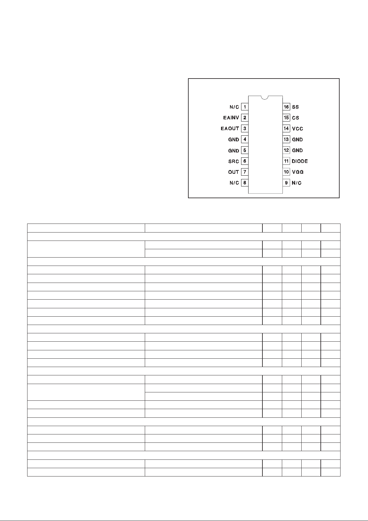
CONNECTION DIAGRAM
Note: The four GND pins are internally connected.
DIL-16, SOIC-16 (Top View)
N or DP Packages
VCC. . . . . . . . . . . . . . . . . . . . . . . . . . . . . . . . . . . . . . . . . . +72V
EAINV . . . . . . . . . . . . . . . . . . . . . . . . . . . . . . . . . –0.3V to +10V
EAOUT . . . . . . . . . . . . . . . . . . . . . . . . . . . . . . . . –0.3V to +10V
SS . . . . . . . . . . . . . . . . . . . . . . . . . . . . . . . . . . . . –0.3V to +10V
DIODE . . . . . . . . . . . . . . . . . . . . . . . . . . . . . . . . . –0.3V to VCC
VGG . . . . . . . . . . . . . . . . . . . . . . . . . . . . . . –0.3V to VCC +14V
CS. . . . . . . . . . . . . . . . . . . . . . . . . . . . VCC – 5V to VCC +0.6V
I
OUT
Pulsed . . . . . . . . . . . . . . . . . . . . . . . . . . . . –0.8A to +0.6A
SRC . . . . . . . . . . . . . . . . . . . . . . . . . . . . . . . . . . . –0.6V to VCC
Storage Temperature . . . . . . . . . . . . . . . . . . . −65°C to +150°C
Junction Temperature. . . . . . . . . . . . . . . . . . . –55°C to +150°C
Lead Temperature (Soldering, 10 sec.). . . . . . . . . . . . . +300°C
Currents are positive into, negative out of the specified terminal.
Consult Packaging Section of Databook for thermal limitations
and considerations of packages.
ABSOLUTE MAXIMUM RATINGS
3
UC2578
UC3578
ELECTRICAL CHARACTERISTICS:
Unless otherwise specified VCC = 14V, VGG = 14V, TA=TJ.
PARAMETER TEST CONDITIONS MIN TYP MAX UNITS
VGG Regulator Section
VGG – SRC VCC = 72V, SRC = 0V, I
VGG
= –7mA 14.5 15.25 17 V
VCC = 50V, SRC = 0V, I
VGG
= –7mA 14 14.75 16 V
VCC = 15V, SRC = 0V, I
VGG
= –7mA 13 13.75 14.5 V
VCC = 11V, SRC = 0V, I
VGG
= –7mA 9.5 10 10.5 V
Soft Start Ramp Section
Soft Start Ramp Current –30 –45 µA
Supply Current Section
I
VCC
EAINV ≥ 2.1V, SRC = 0V 10 14 mA
I
VGG
EAINV ≥ 2.1V, SRC = 0V 7 10.5 mA
CS: Peak current limit sense pin. Senses the current
across a current sense resistor placed between VCC and
the drain of the NMOS buck switch. OUT will be held low
(NMOS buck switch off) if VCC – CS exceeds 0.5V.
DIODE: An external small signal diode (1N4148 typical)
is connected here, anode to VCC and cathode to
DIODE, to implement the VGG regulator function.
EAINV: Inverting input to error amplifier. V
OUT
sense
feedback is connected to this pin. The non-inverting input
of the error amplifier is internally connected to 2V.
EAOUT: Output of the error amplifier. Use EAOUT and
EAINV for loop compensation components.
GND: Circuit Ground. The four ground pins are internally
connected together by the fused leadframe of the
package. They provide the primary thermal conduction
path for dissipating junction heat.
OUT: Gate drive for the external NMOS switch
connected between VCC and the buck inductor.
SRC: This pin is connected to the junction of the external
NMOS switch source, the floating voltage source
capacitor, the free-wheeling diode cathode, and buck
inductor.
SS: The external soft start capacitor is connected to this
pin.
VGG: An external capacitor connected from VGG to
SRC completes the floating voltage source for the
floating gate driver. A1µF capacitor is recommended.
VCC: Input supply voltage. This pin supplies an internal
ground referenced voltage regulator that supplies the IC
and an on-chip regulated floating voltage source (VGG –
SRC) used by the floating driver to drive the external
NMOS buck switch. This pin should be bypassed with a
high quality ceramic capacitor.
PIN DESCRIPTIONS
The UC3578 Floating Buck Controller is a high frequency
switching regulator with a floating driver which provides
PWM control for non-isolated buck converters. The controller operates at a fixed 100 kHz switching frequency,
and in voltage mode control. The duty cycle range of the
PWM output is 0% to 90% allowing for a wide range of
input voltages (14V minimum with transients to 72V).
The regulator features an undervoltage lockout threshold
of 11V with approximately 2V hysterisis as well as soft
start capability. The typical application circuit shown is for
a 15V to 40V input and a 12V at 3A output.
To ensure proper operation of the floating driver, an external capacitor (1µF ceramic) must be connected from
VGG to SRC, and to the source of the external MOSFET
through a small resistor, as shown in the typical application diagram and in Fig 2. This capacitor provides the energy for the high side driver. The gate drive voltage to
the MOSFET is internally regulated to 14V. A diode
(1N4148) is required from the input voltage to DIODE.
This allows the floating drive capacitor to charge during
conduction of the output rectifier but prevents its discharge back into the supply rail. A 1µF ceramic capacitor
is recommended from VCC to ground to provide high frequency decoupling. Additional decoupling of this pin
could be accomplished by a low value resistor between
VCC and V
IN
anda1µF capacitor from VCC to GND as
shown in the schematic.
APPLICATION INFORMATION

4
UC2578
UC3578
Current Limit
The current sense pin provides overcurrent shutdown.
As can be seen from the block diagram, the overcurrent
comparator is wire ANDed with the oscillator after an internally set blanking time. The I
LIMIT
threshold level is set
by the current sense resistor from R
SENSE
.
I
V
R
LIMIT
SENSE
=
05.
An optional filter can be added (RSCS) from the current
sense resistor to CS to provide high frequency filtering of
the current sense signal if necessary.
During a current limit condition, the soft start capacitor on
SS is discharged until its voltage level reaches 1.2V. During this time, a duty cycle clamp is activated to approximately 0.6V above the voltage level on the SS capacitor.
This condition persist until the SS capacitor is discharged
to 1.2V, thus disabling the output driver. At this time, the
SS capacitor is allowed to charge to 5V through the 50µA
current source and normal operation resumes when the
SS capacitor reaches 5V. During the condition described,
the regulator enters a hiccup current limit mode of operation which limits the power dissipation in the MOSFET
and output rectifier under a short circuit condition.
Error Amplifier
The onboard error amplifier of the UC3578 is a voltage
amplifier with its non-inverting input tied to an internal 2V
reference. As usual, loop compensation can be added
from the inverting input of EAINV to the error amplifier
output at EAOUT. Consideration must be given when
choosing the values of the compensation components
around the amplifier so that the output swing of the amplifier is not restricted. The output of the amplifier can
source 100µA typically.
General
As in any buck converter, when the switch is off, the
source flies low due to the conduction of the
free-wheeling rectifier. The source (SRC) is pulled below
ground by an amount determined by the forward voltage
drop of the rectifier and by any transient voltage spike
from inductance in this path. The occurrence of this condition could result in erratic operation of the IC during this
period if the negative excursion is not limited. This is because of conduction of current in the substrate of the IC
due to the source pin being pulled below ground and forward biasing the internal substrate PN junction. To limit
this effect, a small resistor (15Ω) can be placed in series
between the MOSFET source and the SRC pin as shown
in Fig. 1. Too large a resistor will limit the drive to the
Figure 1. Block diagram.
APPLICATION INFORMATION (cont.)
UDG-97006

5
UC2578
UC3578
MOSFET and result in startup problems with the regulator. A Schottky rectifier is used for the free-wheeling diode to limit the negative excursion of the source. This will
also limit the reverse recovery current thus limiting the inductive voltage spike.
In applications where transient load excursions may result in a no load condition, it is necessary that the output
of the regulator be loaded with a small load current
(10mA to 15mA). This will prevent the output voltage
from going unregulated at no load. This small load current is necessary for proper operation of the floating
driver since the source must fly low to charge up the
floating driver capacitance.
Thermal Considerations
For proper operation and reliability of the UC3578,
proper thermal management is essential. It is important
that the designer keep in mind that with surface mount
packages, a significant amount of the heat that the device generates is conducted out through the lead frame.
Because of this, the PCB design becomes a critical part
of the thermal management system. Worst case junction-to-ambient thermal resistance for different package
configurations are given in a table in the data book in the
package information section.
The maximum ambient operating temperature is an important factor in determining what the maximum operating voltage can be for a particular application. For
example, if we assume a maximum operating ambient
temperature of 70°C we can determine what the maximum allowable input voltage can be given other parameters such as package thermal impedance and MOSFET
total gate charge by following the procedure outlined below;
()
TTCCC
J
A
max
––=° °=°125 70 55
. (1)
Pd=
55 C
58 C / W
=0.95W
°
°
,
(2)
where 58°C/W is the worst case theta j-a for the 16 pin
DP package and Pd is the package power dissipation.
1
2
3
4
5
6
7
8
16
15
14
13
12
11
10
9
1µF
470pF
0.1µF
0.01µF
1N4148
N/C
EAINV
EAOUT
GND
GND
SRC
OUT
N/C
SS
CS
VCC
GND
GND
DIODE
VGG
N/C
UC3578
330
0.1µF0.1µF
8.25k
5.62k
2200µF2200µF
680pF
51
1
2
10
30µH
470
200
13
1N4148
5
220µF
220µF
VIN(–)
V
IN
(+)
15k
TIP47
1N4745A
47µF
47k
2200pF
100pF
2
3
1
HS3
23
1
HS1
IRF530
V
OUT
(–)
V
OUT
(+)
HS1, HS2, HS3: HEATSINKS
HS2
MBR10100
Figure 2. Detailed application schematic for the UC3578 evaluation board.
APPLICATION INFORMATION (cont.)
UDG-99100

6
UC2578
UC3578
UNITRODE CORPORATION
7 CONTINENTALBLVD. • MERRIMACK, NH 03054
TEL. (603) 424-2410 FAX (603) 424-3460
0
5
10
15
20
25
30
0 1020304050607080
VCC (V)
ICC (mA)
-55°C
-25°C
25°C
85°C
125°C
Figure 3. ICCvs. VCC vs. temperature.
()
Pd Qg kHz mA V
IN
=• + •100 19
,
(3)
where Qg is the total MOSFET gate charge and 19mA is
the maximum quiescent current for the UC3578 (I
CC
+
I
GG
) from the data sheet. The switching frequency of the
buck converter is 100kHz.
The gate charge can be determined from the MOSFET
data sheet. As an example, for a IRFZ34 which has a total gate charge of 46nC, substituting for Pd in equation 3:
()
0 95 46 100 19.
WnCkHzmAV
IN
=• +•
, and
()
V=
0.95W
0.0236A
= 40V
IN
max
.
Therefore, at 70°C using a IRFZ34 MOSFET the maximum input voltage is limited to 40V to maintain a maximum junction temperature of 125°C in the 16 pin DP
package.
Higher input voltages can be achieved by choosing a
MOSFET with a lower total gate charge or by a reduced
ambient operating temperature or by reducing the theta
j-a of the package by improving the PCB mounting
method. It is recommended that the four GND pins (4, 5,
12 and 13) be connected to a ground plane to provide a
low resistance thermal path. If a ground plane is not
available, a heat spreader on a double sided PC board is
recommended.
Note: Thermal impedance number is based on device
mounted to 5 square inch FR4 PC board with one ounce
copper. From Unitrode 95-96 data book Table 1, page
9-8, when resistance range is given, lower thermal impedance values are for 5 square inch aluminum PC
board.
ADDITIONAL INFORMATION
Please refer to the following Unitrode topic for additional
application information.
[1] Application Note U-167,
Design and Evaluation of a
48V to 5V Telecom Buck Converter using the UC3578
Control IC
by Mark Dennis.
APPLICATION INFORMATION (cont.)

IMPORTANT NOTICE
T exas Instruments and its subsidiaries (TI) reserve the right to make changes to their products or to discontinue
any product or service without notice, and advise customers to obtain the latest version of relevant information
to verify, before placing orders, that information being relied on is current and complete. All products are sold
subject to the terms and conditions of sale supplied at the time of order acknowledgement, including those
pertaining to warranty, patent infringement, and limitation of liability.
TI warrants performance of its semiconductor products to the specifications applicable at the time of sale in
accordance with TI’s standard warranty. Testing and other quality control techniques are utilized to the extent
TI deems necessary to support this warranty. Specific testing of all parameters of each device is not necessarily
performed, except those mandated by government requirements.
CERT AIN APPLICATIONS USING SEMICONDUCT OR PRODUCTS MAY INVOLVE POTENTIAL RISKS OF
DEATH, PERSONAL INJURY, OR SEVERE PROPERTY OR ENVIRONMENTAL DAMAGE (“CRITICAL
APPLICATIONS”). TI SEMICONDUCTOR PRODUCTS ARE NOT DESIGNED, AUTHORIZED, OR
WARRANTED TO BE SUITABLE FOR USE IN LIFE-SUPPORT DEVICES OR SYSTEMS OR OTHER
CRITICAL APPLICATIONS. INCLUSION OF TI PRODUCTS IN SUCH APPLICA TIONS IS UNDERSTOOD T O
BE FULLY AT THE CUSTOMER’S RISK.
In order to minimize risks associated with the customer’s applications, adequate design and operating
safeguards must be provided by the customer to minimize inherent or procedural hazards.
TI assumes no liability for applications assistance or customer product design. TI does not warrant or represent
that any license, either express or implied, is granted under any patent right, copyright, mask work right, or other
intellectual property right of TI covering or relating to any combination, machine, or process in which such
semiconductor products or services might be or are used. TI’s publication of information regarding any third
party’s products or services does not constitute TI’s approval, warranty or endorsement thereof.
Copyright 1999, Texas Instruments Incorporated
 Loading...