

Datasheet UC3904N, UC3904DWTR, UC3904DW, UC2904J, UC2904DW Datasheet (Texas Instruments)
...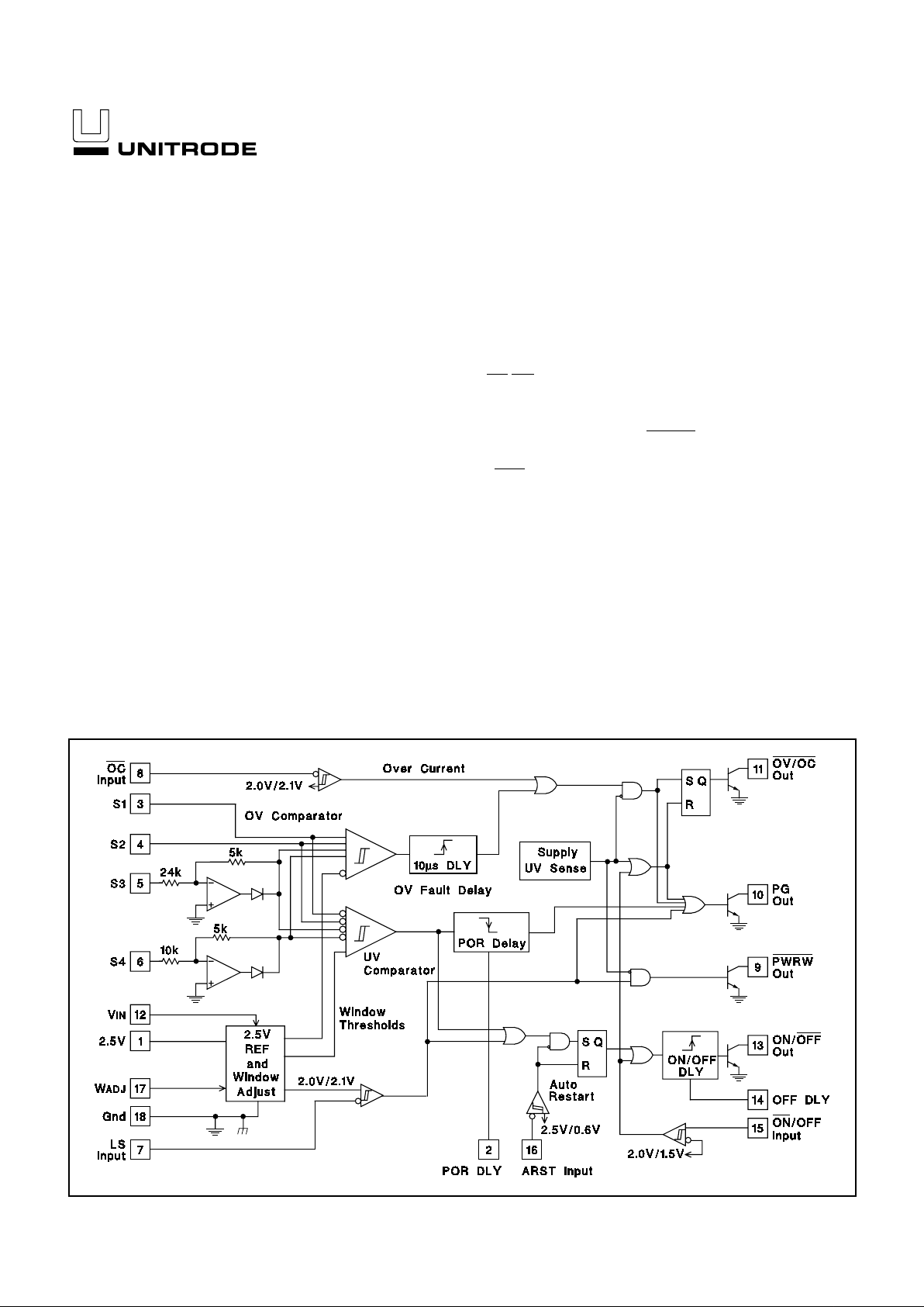
BLOCK DIAGRAM
Note: Pin Numbers refer to J, N, and DW Packages.
4/97
The UC1904 Quad Supp ly Moni tor will respo nd to un der- and over-voltage conditi o ns on u p to four c on ti nu ou s ly m on itor ed voltage levels. Four
independen t positive voltages can be monitor ed or, alternatively, two of
the sense in puts are preset t o monitor -5V and -12V supplies. The device also monitors Over-Current and Line Sense inputs, both with precision input thresholds.
Four open collector outputs on the UC1904 give the following responses: 1. The
OV/OC output is a l a tc h ed over-voltag e, or over-current
response. 2. A Power Good signal responds low with any fault detection
– on power-up a pro grammable delay is use d to hol d this output low for
a system Power On Reset signal. 3. The
PWRW output responds only to
a Line Sense inp ut, for ea rl y warning of power failu res. 4. The last open
collector, the ON/
OFF output, gener ates a delayed supply OFF control
signal in re sponse to an OFF input comma nd, under-voltage condition,
or line fault detection.
The OV-UV fault window is adjustable with a programming input. The
thresholds are centered around the precision 2.5V reference, with a
scaled hystere sis for precise, glitch free operation. In the positive mode
of operation, the fault windows at each of the sens e inputs can be independently s c a l ed u sing external resis tors and the 2.5V r eference output.
An Auto Restar t functio n couples with the under-voltage and line sensing circuits to allow controlled power supply start-up and shutdown.
This device will operate over a supply range of 4.75V to 18V. The device
is available in a DIP, SOIC, or PLCC outline. This device is ESD protected on all pins.
• Inputs for Monitoring Up to Four
Supply Voltages
• Two Inputs Preset for -5V and -12V
Monitoring, or Programmable
Positive Levels
• Precision 2.5V Reference
• Separate Inputs for Over-Current and
Line Fault Sensing
• Adjustable Under- to Over-Voltage
Fault Windows
• Latched Over-Voltage and
Over-Current Output
• Power Good and Power Warning
Outputs
• Auto Restart Function with ON/OFF
Control, and Programmable Delay
• Programmable Pwr On Reset Delay
UC1904
UC2904
UC3904
Precision Quad Supply and Line Monitor
FEATURES
DESCRIPTION
UC1904
UC2904
UC3904
Input Supply Voltage . . . . . . . . . . . . . . . . . . . . . . . . . . . . . . 20V
Sense Inputs, S1 And S2, Other Analog And Logic Inputs
Maximum Forced Voltage . . . . . . . . . . . . . . . . . . -0.3V to 10V
Maximum Forced Current . . . . . . . . . . . . . . . . . . . . . . ±10mA
Sense Input S3, (-12V Sense Input)
Maximum Forced Voltage . . . . . . . . . . . . . . . . . . -18V to 10V
Maximum Forced Current . . . . . . . . . . . . . . . . . . . . . . ±10mA
Sense Input S4, (-5V Sense Input)
Maximum Forced Voltage . . . . . . . . . . . . . . . . . . -10V to 10V
Maximum Forced Current . . . . . . . . . . . . . . . . . . . . . . ±10mA
Open Collector Outputs
Maximum Voltage . . . . . . . . . . . . . . . . . . . . . . . . . . . . . . . 20V
Maximum Current . . . . . . . . . . . . . . . . . . . . . . . . . . . . . 50mA
Reference Output Current . . . . . . . . . . . . . . . Internally Limited
Operating Junction Temperature . . . . . . . . . . . -55°C to +150°C
Storage Temperature . . . . . . . . . . . . . . . . . . . . -65°C to +150°C
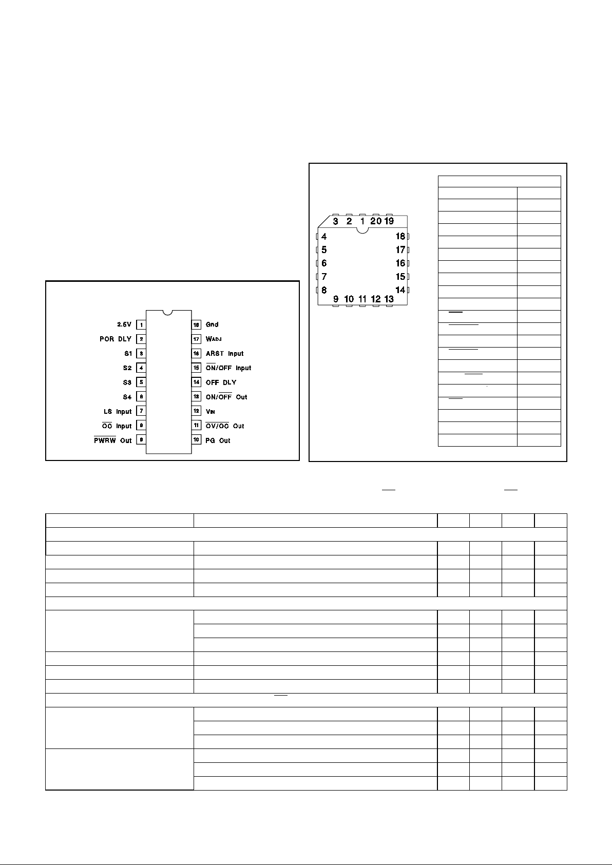
PACKAGE PIN FUNCTION
FUNCTION PIN
2.5V 1
POR DLY 2
N.C. 3
S1 4
S2 5
S3 6
S4 7
N.C. 8
LS Input 9
OC Input 10
PWRW Out 11
PG Out 12
OV/OC Out 13
V
IN
14
ON/
OFF Out 15
OFF DLY
16
ON/OFF Input 17
ARST Input 18
W
ADJ
19
Gnd 20
DIL-18, SOIC-18 (TOP VIEW)
J or N PACKAGE, DW PACKAGE
PLCC-20 (TOP VIEW)
Q PACKAGE
CONNECTION DIAGRAMS
ABSOLUTE MAXIMUM RATINGS
(Note 1)
Note 1: Unless otherwise indicated, voltages are reference to
ground and currents are positive into, negative out of, the specified terminals.
Unless otherwise stated, these specifications hold for TA = 0 to 70°C for the
UC3904, -40 to +85°C for the UC2904, and -55 to +1 25°C for the UC1904, +VIN =
15V, W
ADJ
= 0.5V, Sense Inputs 1-4, OC and LS Inputs = 2.5V. The ON/OF F In pu t
and the ARST Input = 0V.
ELECTRICAL CHARACTERISTICS:
PARAMETER TEST CONDITIONS MIN TYP MAX UNITS
Input Supply
V
IN
Supply Current VIN = 15V 3.2 4.5 mA
V
IN
UVLO Threshold Low to High 4.5 4.75 V
UVLO Threshold Hysteresis 50 mV
Minimum VIN to Enable PG Out 0.8 1.5 V
Reference
Output Voltage(V
REF
)T
J
= 25°C 2.475 2.5 2.525 V
Over Temperature, UC3904 2.47 2.53 V
Over Temperature, UC2904 & UC1904 2.465 2.535 V
Load Regulation I
OUT
= 0 to 4mA 6 mV
Line Regulation V
IN
= 4.75 to 18V 5 mV
Short Circuit Current V
REF
= 0V 17 mA
OV UV Window, LS Input, OC Input, ARST Input, and
ON/OFF Input Thresholds
Over-Voltage Thresholds W
ADJ
= 0.25V, Offset from V
REF
, Input L to H 110 125 140 mV
S1, S2 W
ADJ
= 0.5V, Offset from V
REF
, Input L to H 230 250 270 mV
W
ADJ
= 1V, Offset from V
REF
, Input L to H 460 500 540 mV
Over-Voltage Thresholds W
ADJ
= 0.25V, Offset from V
REF
, Input L to H 110 125 145 mV
S3, S4 Positive Mode W
ADJ
= 0.5V, Offset from V
REF
, Input L to H 230 250 280 mV
W
ADJ
= 1V, Offset from V
REF
, Input L to H 460 500 550 mV
2

UC1904
UC2904
UC3904
PARAMETER TEST CONDITIONS MIN TYP MAX UNITS
OV UV Window, LS Input, OC Input, ARST Input, and
ON/OFF Input Thresholds (cont.)
Under-Voltage Threshold s W
ADJ
= 0.25V, Offset from V
REF,
Input H to L -140 -125 -110 mV
S1, S2 W
ADJ
= 0.5V, Offset from V
REF,
Input H to L -270 -250 -230 mV
W
ADJ
= 1V, Offset from V
REF,
Input H to L -540 -500 -460 mV
Under-Voltage Threshold s W
ADJ
= 0.25V, Offset from V
REF,
Input H to L -150 -125 -110 mV
S3, S4 Positive Mode W
ADJ
= 0.5V, Offset from V
REF,
Input H to L -285 -250 -230 mV
W
ADJ
= 1V, Offset from V
REF,
Input H to L -555 -500 -460 mV
OV and UV Threshold Hysteresis As a Function of W
ADJ
30 50 70 mV/V
S3 Negative Mode Thresholds Over-Voltage , W
ADJ
= 0.5V, Input H to L -13.52 -13.2 -12.88 V
Under-Voltage, W
ADJ
= 0.5V, Input L to H -11.06 -10.8 -10.54 V
Hysteresis, W
ADJ
= 0.5V 80 120 160 mV
S4 Negative Mode Thresholds Over-Voltage , W
ADJ
= 0.5V, Input H to L -5.63 -5.5 -5.37 V
Under-Voltage, W
ADJ
= 0.5V, Input L to H -4.61 -4.5 -4.39 V
Hysteresis, W
ADJ
= 0.5V 30 50 70 mV
W
ADJ
Input Bias Current 0.25V < W
ADJ
<1.0V -5 5
µ
A/V
LS Threshold Input = H to L 1.96 2 2.04 V
Threshold hysteresis 65 100 125 mV
OC Threshold Input = H to L 1.9 2 2.1 V
Threshold hysteresis 50 100 150 mV
ARST Input Threshold Input = L to H 2.25 2.5 2.75 V
Input = H to L 0.56 0.625 0.69 V
ON/OFF Input Threshold Input high level 1.74 2.4 V
Input low level 0.6 1.35 V
Sense and Logic Input Bias Currents
Sense 1-4, Positive Mode Input = 2.8V 250 800 nA
Input = 2.2V -1000 -250 nA
Sense 3 Negative Mode Input = -12V -700 -500 -300
µ
A
Sense 4 Negative Mode Input = -5V -700 -500 -300
µ
A
Line, and OC Inputs Input = 2.2V 300 1000 nA
ON/OFF Input In pu t = 2.5V 150 600 nA
ARST Input Input = 0.5 -2000 -700 nA
Open Collector Outputs (
OV/OC Out, PG Out, PWRW Out, ON/OFF Out)
Saturation Voltage I
OUT
= 10mA 0.2 0.4 V
Leakage current V
OUT
= 20V 5
µ
A
POR Delay
Delay 160 250 350 ms/µF
Internal Pullup Current 9
µ
A
Threshold Low to High 2.25 V
OFF Delay
Delay 120 185 250 ms/µF
Internal Pullup current 12
µ
A
Threshold Low to High 2.25 V
OV Fault Delay
Delay 10 20 50
µ
s
Unless otherwise stated, these specifications hold for T
A
= 0 to 70°C for the UC3904, -40 to
+85°C for the UC2904, and -55 to +1 25°C for the UC1904, +VIN = 15V, W
ADJ
= 0.5V, Sense
Inputs 1-4, OC and LS Inputs = 2.5V. The ON/OFF Input and the ARST Input = 0V.
ELECTRICAL
CHARACTERISTICS (cont):
3

PIN FUNCTIONAL DESCRIPTION
2.5V: This is the output of the precision 2.5V reference.
ARST Input: This input, with a 4:1 hystereti c threshold,
is used to sequence a power system through the Auto
ReStarT cycle. A delayed representation of a supply out-
put voltage is used at this pin to provide adequate startup
time for the power system, and a minimum power-off period.
Gnd: Reference point for the internal reference and all
thresholds, as well as the return for the remainder of the
device.
LS Input: The Line Sense input is used to monitor a volt-
age that varies with the input line voltage to a system.
The input is compared to a precision 2.0V level and is
used to acti vate the
PWRW and PG outputs, as well as
triggering the Auto Restart sequence.
OC Input: The Over -Current input can be used to re-
spond to an invert ed over-current signal. A low level signal at this i nput la tches in a fault indication at the
OV/OC
output.
OFF DLY: This pin functions similarly to the POR DLY
pin to delay the turn-on of the ON/
OFF output trans istor.
The charging current an d upper thre shold are 12µA and
2.1V.
ON/OFF Input: With a high level at this input the
ON/
OFF Out pin is acti vated af ter a user-programmable
delay. A high level also activates the PG Out pin, and r esets the OV/OC fault latch.
On/
Off Out: This output is a n open collector output that
is activated by the
ON/OFF Input, or the Auto Restart circuitr y. Saturation voltage on this and all the open collector outputs is rated at 10mA of current.
OV/OC Out: In response to either an Over -Voltage or
Over-Current situation this output is latched active low.
There is nominal 20µ s delay in the OV path to the fault
latch, providi ng reje ctio n to transient overshooting on the
monitored voltages. The low condition is cleared when
the fault latch is reset by the
ON/OFF In put, or a UVLO
condition on the device.
POR DLY: This pin is used, w i th an exter n al capac itor, to
program a Power-On-Reset delay. This delay is reset
whenever there is a U V co nditi on at one of the S1-S4 inputs, and then triggered upon the clearing of the UV condition. When reset, the voltage across the capacitor is
quickly discharged to near zero volts, and the PG Out pin
goes active low. Once triggered the capacitor is charged
by a 9µA cur rent source. The PG Out pin remains active
low until the delay capacitor voltage reaches a 2.1V
threshold.
PG Out: During any fault, under-voltage, or UVLO condition this output is low. A Power Good indicati on (output
off) is given when all suppl y conditions are within defined
operating limits. During power-up the PG signal is delayed by a programmable Power O n Reset delay. During
UVLO the output i s active low as long as the input s upply, V
IN
, is above approximately 1.0V.
PWRW Out: When a low line condition is sensed by the
LS Input this output goes low. This output is disabled
(off) during a UVLO condition.
S1-S4: These are the sense inputs for OV and UV moni-
toring of external volt ages. All four inputs can be used to
sense posi tive volt ag es with a simple di vi d er t o s cale the
voltage level to the 2.5V centered window. The S3 and
S4 inputs can al so be used to sense -12V and -5V supplies respectively with no external components. This is
done with internal precision resistor dividers and two
source only op-amps that are dis abled when the pins are
used in the positive mode.
V
IN
: Input supply for the UC1904. The device is opera-
tional with 4.75V to 18V on this pin.
W
ADJ
: The W
ADJ
input is us ed to program the OV and
UV window thresholds. The OV-UV window is centered
around the 2.5V reference and is nominally ±20% per
volt on the W
ADJ
input pin.
UC1904
UC2904
UC3904
4

UC1904
UC2904
UC3904
UNITRODE CORPORATION
7 CONTINENTAL BLVD. • MERRIMACK, NH 03054
TEL. (6 03 ) 42 4- 24 10 • FAX (603) 424-3460
Note: Pin Numbers refer to J, N, and DW Packages.
5

IMPORTANT NOTICE
T exas Instruments and its subsidiaries (TI) reserve the right to make changes to their products or to discontinue
any product or service without notice, and advise customers to obtain the latest version of relevant information
to verify, before placing orders, that information being relied on is current and complete. All products are sold
subject to the terms and conditions of sale supplied at the time of order acknowledgement, including those
pertaining to warranty, patent infringement, and limitation of liability.
TI warrants performance of its semiconductor products to the specifications applicable at the time of sale in
accordance with TI’s standard warranty. Testing and other quality control techniques are utilized to the extent
TI deems necessary to support this warranty. Specific testing of all parameters of each device is not necessarily
performed, except those mandated by government requirements.
CERT AIN APPLICATIONS USING SEMICONDUCTOR PRODUCTS MAY INVOLVE POTENTIAL RISKS OF
DEATH, PERSONAL INJURY, OR SEVERE PROPERTY OR ENVIRONMENTAL DAMAGE (“CRITICAL
APPLICATIONS”). TI SEMICONDUCTOR PRODUCTS ARE NOT DESIGNED, AUTHORIZED, OR
WARRANTED TO BE SUITABLE FOR USE IN LIFE-SUPPORT DEVICES OR SYSTEMS OR OTHER
CRITICAL APPLICATIONS. INCLUSION OF TI PRODUCTS IN SUCH APPLICA TIONS IS UNDERSTOOD T O
BE FULLY AT THE CUSTOMER’S RISK.
In order to minimize risks associated with the customer’s applications, adequate design and operating
safeguards must be provided by the customer to minimize inherent or procedural hazards.
TI assumes no liability for applications assistance or customer product design. TI does not warrant or represent
that any license, either express or implied, is granted under any patent right, copyright, mask work right, or other
intellectual property right of TI covering or relating to any combination, machine, or process in which such
semiconductor products or services might be or are used. TI’s publication of information regarding any third
party’s products or services does not constitute TI’s approval, warranty or endorsement thereof.
Copyright 1999, Texas Instruments Incorporated
 Loading...