

Datasheet UC3879N, UC3879J, UC3879DWTR, UC3879DW, UC2879N Datasheet (Texas Instruments)
...
6/98
FEATURES
• Programmable Output Turn On
Delay; Zero Delay Available
• Compatible with Voltage Mode or
Current Mode Topologies
• Practical Operation at Switching
Frequencies to 300kHz
• Four 100mA Totem Pole Outputs
• 10MHz Error Amplifier
• Pin Programmable Undervoltage
Lockout
• Low Startup Current - 150µA
• Soft Start Control
• Outputs Active Low During UVLO
Phase Shift Resonant Controller
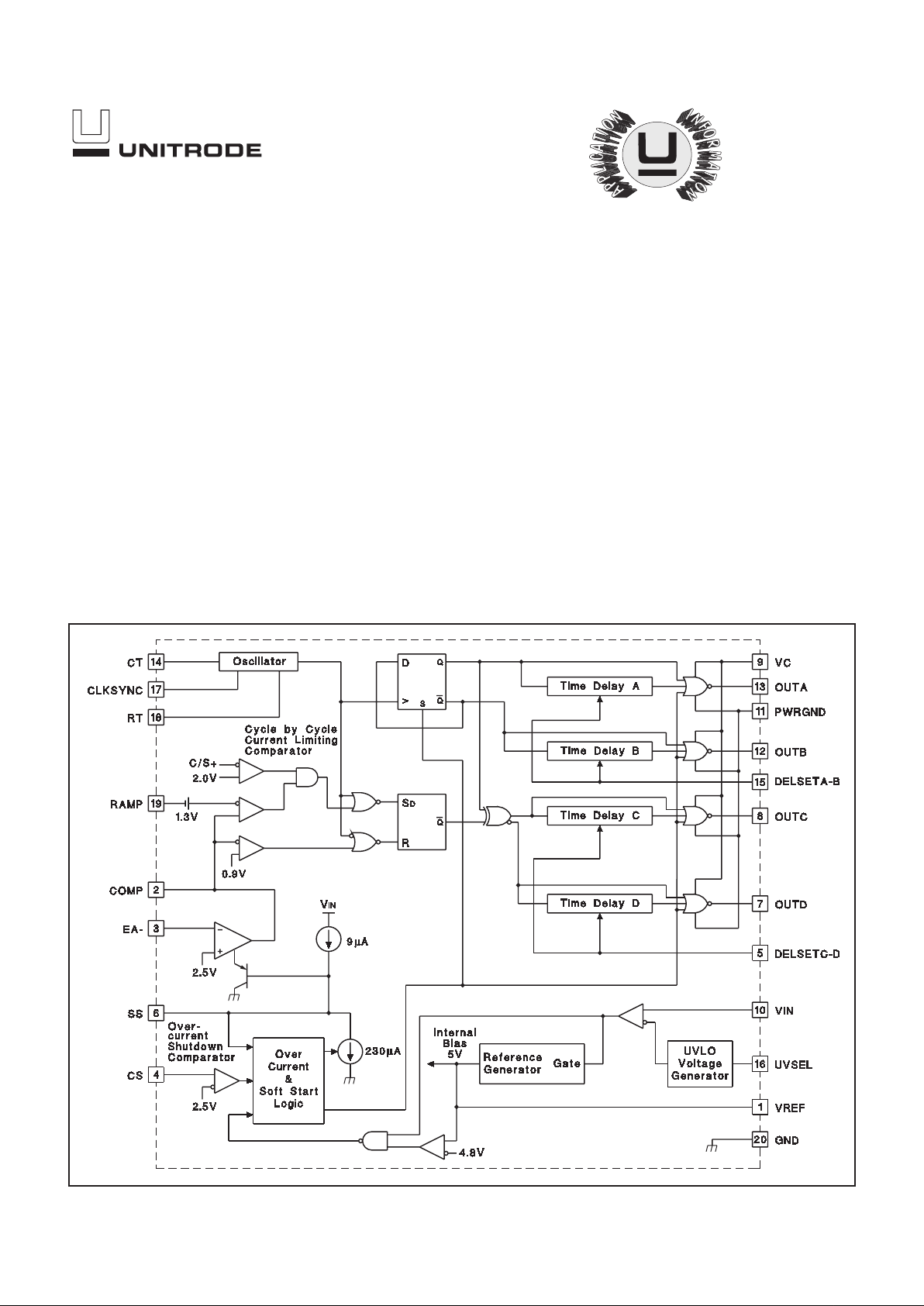
BLOCK DIAGRAM
UDG-94070-1
UC1879
UC2879
UC3879
DESCRIPTION
The UC3879 controls a bridge power stage by phase shifting the switching
of one half-bridge with respect to the other. This allows constant frequency
pulse width modulation in combination with resonant, zero-voltage switching
for high efficiency performance. The UC3879 can be configured to provide
control in either voltage mode or current mode operation, with overcurrent
shutdown for fast fault protection.
Independently programmable time delays provide dead-time at the turn-on
of each output stage, allowing time for each resonant switching interval.
With the oscillator capable of operating in excess of 600kHz, overall output
switching frequencies to 300kHz are practical. In addition to the standard
free running mode, with the CLKSYNC pin, the user may configure the
UC3879 to accept an external clock synchronization signal. Alternatively, up
to three units can be locked together with the operational frequency determined by the fastest device.
Protective features include an undervoltage lockout and overcurrent protection. Additional features include a 10MHz error amplifier, a 5V precision reference, and soft start. The UC3879 is available in 20 pin N, J, DW, and Q
and 28 pin L packages.
2
UC1879
UC2879
UC3879
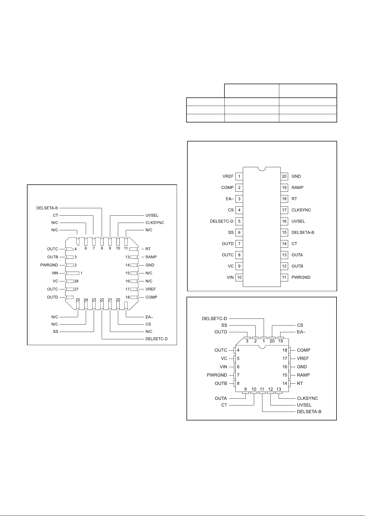
CONNECTION DIAGRAMS
DIL-20, SOIC-20 (Top View)
JorNPackage,DWPackage
ABSOLUTE MAXIMUM RATINGS
Supply Voltage (VC, VIN) ..........................20V
Output Current, Source or Sink, DC.................20mA
Analog I/0s
(Pins 1, 2, 3, 4, 5, 6, 14, 15, 17, 18, 19) ......−0.3 to 5.3V
(Pin 16) ...............................−.03V to VIN
Storage Temperature Range .............−65°C to +150°C
Junction Temperature...................−55°C to +150°C
Lead Temperature (Soldering, 10 sec.) ............ +300°C
Notes: Pin references are to 20 pin DIL and SOIC packages.
All voltages are with respect to ground unless otherwise stated.
Currents are positive into, negative out of the specified terminal. Consult Packaging Section of Databook for thermal limitations and considerations of packages.
PLCC-20 (Top View)
Q Package
Table I. Product Selection Guide
TEMPERATURE
RANGE
AVAILABLE
PACKAGES
UCC1879 – 55°C to +125°C J, L
UCC2879 – 40°C to +85°C N, DW, Q, J, L
UCC3879 0°C to +70°C N, DW, Q
CLCC-28 (Top View)
L Package

3
UC1879
UC2879
UC3879
ELECTRICAL CHARACTERISTICS
Unless specified; VC = VIN = V
UVSEL
=12V, CT = 470pF, RT = 9.53k, RDELSETA-B =
R
DELSEC-D
= 4.8k, C
DELSETA-B=CDELSETC-D
= 0.01µF, TA=TJ.
PARAMETER TEST CONDITIONS MIN TYP MAX UNITS
Undervoltage Lockout
Start Threshold V
UVSEL
= VIN 9 10.75 12.5 V
V
UVSEL
= Open 12.5 15.25 16.5 V
UVLO Hysteresis V
UVSEL
= VIN 1.15 1.75 2.15 V
V
UVSEL
= Open 5.2 6 7.4 V
Input Bias, UVSEL Pin V
UVSEL
=VIN=8V 30 µA
Supply Current
I
VIN
Startup VIN = V
UVSEL
= 8V, VC = 18V, I
DELSETA-B
=
I
DELSETC-D
=0
150 600 µA
IVCStartup VIN = V
UVSEL
= 8V, VC = 18V, I
DELSETA-B
=
I
DELSETC-D
=0
10 100 µA
I
VIN
Operating UC3879, UC2879 23 33 mA
UC1879 23 36 mA
I
VC
Operating 48mA
Voltage Reference
Output Voltage T
J
= +25°C 4.92 5 5.08 V
Line Regulation 11V < VIN < 18V 1 10 mV
Load Regulation I
VREF
= –10mA 5 20 mV
Total Variation Line, Load, Temperature 4.875 5.125 V
Short Circuit Current VREF = 0V, T
J
=25°C –60 –15 mA
Error Amplifier
Error Amplifier Input Voltage 2.4 2.5 2.6 V
Input Bias Current 0.6 3 µA
AVOL 1V < V
COMP
<4V 60 90 dB
PSRR 11V < VIN < 18V 85 100 dB
Output Sink Current V
COMP
= 1V 1 2.5 mA
Output Source Current V
COMP
=4V −1.3 −0.5 mA
Output Voltage High I
COMP
= –0.5mA 4 4.7 5 V
Output Voltage Low I
COMP
= 1mA 0 0.5 1 V
Slew Rate TA= +25°C 6 11 V/µs
PWM Comparator
RAMP Offset Voltage T
J
=25°C, Note 3 1.1 1.25 1.4 V
PWM Phase Shift, V
COMP>VRAMPpeak+VRAMPoffset
98 99.7 102 %
T
DELSETA-B
,
T
DELSETC-D
= 0, Note 1 V
COMP
< Zero Phase Shift Voltage 0 0.3 2 %
Output Skew, V
COMP
>VRAMPpeak +VRAMPoffset 10 ns
T
DELSETA-B
,
T
DELSETC-D
= 0, Note 1 V
COMP
< Zero Phase Shift Voltage 10 ns
Ramp to Output Delay, T
DELSETA-B
=0,
T
DELSETC-D
=0
UC3879, UC2879 115 250 ns
UC1879 115 300 ns
Oscillator
Initial Accuracy T
A
=25°C 180 200 220 kHz
Voltage Stability 11V < VIN < 18V 1 2 %
Total Variation Line, Temperature 160 200 240 kHz
CLKSYNC Threshold 2.3 2.5 2.7 V
Clock Out High 2.8 4 V
Clock Out Low 0.5 1 1.5 V
Clock Out Pulse Width 400 600 ns
Ramp Valley Voltage 0.2 0.4 V

4
UC1879
UC2879
UC3879
Note 1. Phase shift percentage (0% = 0°, 100% = 180°)isde-
fined as
θ=
200
T
Φ
%
where
θ
is the phase shift, andΦand T are defined in Figure 1.
At 0% phase shift,
Φ
is the output skew.
Note 2. Delay time is defined as:
delay T duty cycle
=•
1
2
where T is defined in Figure 1.
Note 3. Ramp offset voltage has a temperature coeffecient of
about –4mV/
°
C.
Note 4. The zero phase shift voltage is the voltage measured
at COMP which forces zero phase shift. This condition corresponds to zero effective output power. Zero phase shift voltage
has a temperature coeffecient of about –2mV/
°
C.
Note 5. Delay time can be programmed via resistors from the
delay set pins to ground.
()
Delay Time R
DELAY
=••
−
089 10
10
.sec
The recommended range for R
DELAY
is 1.9k to 10k.
Figure 1. Phase Shift, Output Skew & Delay Time
Definitions
Duty Cycle =
t
T
Period=T
T
DHL
(A to C) = T
DHL
(B to D) =
Φ
ELECTRICAL CHARACTERISTICS Unless specified; VC = VIN = V
UVSEL
=12V, CT = 470pF, RT = 9.53k, RDELSETA-B =
R
DELSEC-D
= 4.8k, C
DELSETA-B=CDELSETC-D
= 0.01µF, TA=TJ.
PARAMETER TEST CONDITIONS MIN TYP MAX UNITS
Ramp Peak Voltage 2.8 2.9 3.2 V
Current Limit
Input Bias V
CS
= 3.0V 2 10 µA
Threshold Voltage 2.35 2.5 2.65 V
Delay to OUTA, B, C, D 160 300 ns
Cycle-by-Cycle Current Limit
Input Bias V
CS
= 2.2V 2 10 µA
Threshold Voltage 1.85 2 2.15 V
Delay to Output Zero Phase 110 300 ns
Soft Start/Reset Delay
Charge Current V
SS
= 0.5V –20 –9 –3 µA
Discharge Current VSS= 1V 120 230 µA
Restart Threshold 4.3 4.7 V
Discharge Level 300 mV
Output Drivers
Output Low Level I
OUT
= 10mA 0.3 0.4 V
Output High Level I
OUT
= –10mA, Referenced to VC 2.2 3 V
Delay Set (Note 5)
Delay Time R
DELSETA-B=RDELSETC-D
= 4.8k 300 430 600 ns
Delay Time R
DELSETA-B=RDELSETC-D=
1.9k 130 170 250 ns
Zero Delay V
DELSETA-B=VDELSETC-D
=5V 5 ns

5
UC1879
UC2879
UC3879
PIN DESCRIPTIONS
CLKSYNC (Bi-directional Clock and Synchronization):
Used as an output, CLKSYNC provides a clock signal. As
an input, this pin provides a synchronization point.
Multiple UC3879s, each with their own local oscillator
frequency, may be connected together by the CLKSYNC
pin, and they will synchronize to the fastest oscillator.
This pin may also be used to synchronize the UC3879 to
an external clock, provided the frequency of the external
signal is higher than the frequency of the local oscillator.
CLKSYNC is internally connected to an emitter follower
pull-up and a current source pull-down (300µA typical).
Therefore an external resistor to GND can be used to
improve the CLKSYNC pin’s ability to drive capacitive
loads.
COMP (Error Amplifier Output): This pin is the output of
the gain stage for overall feedback control. Error amplifier
output voltage levels below 0.9 volt forces zero phase
shift. Since the error amplifier has a relatively low current
drive capability, the output may be overridden by driving it
with a sufficiently low impedance source.
CT (Oscillator Frequency Set): After choosing RT to set
the required upper end of the linear duty cycle range, the
timing capacitor (CT) value is calculated to set the
oscillator frequency as follows:
CT
Dlin
RT f
=
••
108.
Connect the timing capacitor directly between CT and
GND. Use a high quality ceramic capacitor with low ESL
and ESR for best results. A minimum CT value of 200pF
insures good accuracy and less susceptibility to circuit
layout parasitics. The oscillator and PWM are designed to
provide practical operation to 600kHz.
CS (Current Sense): This pin is the non-inverting input to
the two current fault comparators whose references are
set internally to fixed values of 2.0V and 2.5V. When the
voltage at this pin exceeds 2.0V, and the error amplifier
output voltage exceeds the voltage on the ramp input, the
phase shift limiting overcurrent comparator will limit the
phase shifting on a cycle-by-cycle basis. When the
voltage at this pin exceeds 2.5V, the current fault latch is
set, the outputs are forced OFF, and a soft start cycle is
initiated. If a constant voltage above 2.5V is applied to
this pin the outputs are disabled and held low. When CS
is brought below 2.5V, the outputs will begin switching at
0 degrees phase shift before the SS pin begins to rise.
This condition will not prematurely deliver power to the
load.
DELSETA-B, DELSETC-D (Output Delay Control): The
user programmed currents from these pins to GND set
the turn on delay for the corresponding output pair. This
delay is introduced between the turn off of one switch
and the turn on of another in the same leg of the bridge
to allow resonant switching to take place. Separate
delays are provided for the two half-bridges to
accommodate differences in the resonant capacitor
charging currents.
EA– (Error Amplifier Inverting Input): This is normally
connected to the voltage divider resistors which sense
the power supply output voltage level. The loop
compensation components are connected between this
pin and COMP.
GND (Signal Ground): All voltages are measured with
respect to GND. The timing capacitor on CT, and bypass
capacitors on VREF and VIN should be connected
directly to the ground plane near GND.
OUTA – OUTD (Outputs A-D): The outputs are 100mA
totem pole output drivers optimized to drive FET driver
ICs. The outputs operate as pairs with a nominal 50%
duty cycle. The A-B pair is intended to drive one
half-bridge in the external power stage and is
synchronized to the clock waveform. The C-D pair drives
the other half-bridge with switching phase shifted with
respect to the A-B outputs.
PWRGND (Power Ground): VC should be bypassed with
a ceramic capacitor from VC to the section of the ground
plane that is connected to PWRGND. Any required bulk
reservoir capacitor should be connected in parallel.
PWRGND and GND should be connected at a single
point near the chip to optimize noise rejection and
minimize DC voltage drops.
RAMP (Voltage Ramp): This pin is the input to the PWM
comparator. Connect it to CT for voltage mode control.
For current mode control, connect RAMP to CS and also
to the output of the current sense transformer circuit.
Slope compensation can be achieved by injecting a
portion of the ramp voltage from CT to RAMP.

6
UC1879
UC2879
UC3879
RT (Clock/Sync Duty Cycle Set Pin): The UC3879
oscillator produces a sawtooth waveform. The rising edge
is generated by connecting a resistor from RT to GND
and a capacitor from CT to GND (see CT pin
description). During the rising edge, the modulator has
linear control of the duty cycle. The duty cycle jumps to
100% when the voltage on COMP exceeds the oscillator
peak voltage. Selection of RT should be done first, based
on the required upper end of the linear duty cycle range
(D
lin) as follows:
()
RT
mA Dlin
=
•
25
10 1.
Recommended values for RT range from 2.5k to 100k.
SS: Connect a capacitor between this pin and GND to
set the soft start time. The voltage at SS will remain near
zero volts as long as VIN is below the UVLO threshold.
Soft start will be pulled up to about 4.8V by an internal
9µA current source when VIN and VREF become valid
(assuming a non-fault condition). In the event of a current
fault (CS voltage exceeding 2.5V), soft start will be pulled
to GND and then ramp to 4.8V. If a fault occurs during the
soft start cycle, the outputs will be immediately disabled
and soft start must fully charge prior to resetting the fault
latch. For paralleled controllers, the soft start pins may be
paralleled to a single capacitor, but the charge currents
will be additive.
UVSEL: Connecting this pin to VIN sets a turn on voltage
of 10.75V with 1.5V of UVLO hysteresis. Leaving the pin
open-circuited programs a turn on voltage of 15.25V with
6.0V of hysteresis.
VC (Output Switch Supply Voltage): This pin supplies
power to the output drivers and their associated bias
circuitry. The difference between the output high drive
and VC is typically 2.1V. This supply should be bypassed
directly to PWRGND with a low ESR/ESL capacitor.
VIN (Primary Chip Supply Voltage): This pin supplies
power to the logic and analog circuitry on the integrated
circuit that is not directly associated with driving the
output stages.Connect VIN to a stable source above 12V
for normal operation. To ensure proper functionality, the
UC3879 is inactive until VIN exceeds the upper
undervoltage lockout threshold. This pin should be
bypassed directly to GND with a low ESR/ESL capacitor.
NOTE:When VIN exceeds the UVLO threshold the supply current (I
IN
) jumps from about 100µA to greater than 20mA.If the
UC3879 is not connected to a well bypassed supply, it may immediately enter the UVLO state again. Therefore, sufficient bypass capacity must be added to ensure reliable startup.
VREF: This pin provides an accurate 5V voltage
reference. It is internally short circuit current limited.
VREF is disabled while VIN is below the UVLO threshold.
The circuit is also disabled until VREF reaches
approximately 4.75V. For best results bypass VREF with
a 0.1µF, low ESR/ESL capacitor.
PIN DESCRIPTIONS (cont.)
UNITRODE CORPORATION
7 CONTINENTAL BLVD. • MERRIMACK, NH 03054
TEL. (603) 424-2410 FAX (603) 424-3460
ADDITIONAL INFORMATION
Please refer to the following Unitrode publications for
additional information. The following three topics are
available in the Applications Handbook.
[1] Application Note U-154,
The New UC3879 PhaseShifted PWM Controller Simplifies the Design of Zero
Voltage Transition Full-Bridge Converters
by Laszlo
Balogh.
[2] Application Note U-136,
Phase Shifted, Zero Voltage
Transition Design Considerations and the UC3875 PWM
Controller
by Bill Andreycak.
Design Note DN-63,
The Current-Doubler Rectifier: An
Alternative Rectification Technique for Push-Pull and
Bridge Converters
by Laszlo Balogh.

IMPORTANT NOTICE
T exas Instruments and its subsidiaries (TI) reserve the right to make changes to their products or to discontinue
any product or service without notice, and advise customers to obtain the latest version of relevant information
to verify, before placing orders, that information being relied on is current and complete. All products are sold
subject to the terms and conditions of sale supplied at the time of order acknowledgement, including those
pertaining to warranty, patent infringement, and limitation of liability.
TI warrants performance of its semiconductor products to the specifications applicable at the time of sale in
accordance with TI’s standard warranty. Testing and other quality control techniques are utilized to the extent
TI deems necessary to support this warranty. Specific testing of all parameters of each device is not necessarily
performed, except those mandated by government requirements.
CERT AIN APPLICATIONS USING SEMICONDUCTOR PRODUCTS MAY INVOLVE POTENTIAL RISKS OF
DEATH, PERSONAL INJURY, OR SEVERE PROPERTY OR ENVIRONMENTAL DAMAGE (“CRITICAL
APPLICATIONS”). TI SEMICONDUCTOR PRODUCTS ARE NOT DESIGNED, AUTHORIZED, OR
WARRANTED TO BE SUITABLE FOR USE IN LIFE-SUPPORT DEVICES OR SYSTEMS OR OTHER
CRITICAL APPLICATIONS. INCLUSION OF TI PRODUCTS IN SUCH APPLICA TIONS IS UNDERSTOOD T O
BE FULLY AT THE CUSTOMER’S RISK.
In order to minimize risks associated with the customer’s applications, adequate design and operating
safeguards must be provided by the customer to minimize inherent or procedural hazards.
TI assumes no liability for applications assistance or customer product design. TI does not warrant or represent
that any license, either express or implied, is granted under any patent right, copyright, mask work right, or other
intellectual property right of TI covering or relating to any combination, machine, or process in which such
semiconductor products or services might be or are used. TI’s publication of information regarding any third
party’s products or services does not constitute TI’s approval, warranty or endorsement thereof.
Copyright 1999, Texas Instruments Incorporated
 Loading...