

UC1611
UC3611
FEATURES
• Matched, Four-Diode Monolith ic Array
• High Peak Current
• Low-Cost MINIDIP Package
• Low-Forward Voltage
• Parallelable for Lower V
F or Higher IF
• Fast Recovery Time
• Military Temperature Range Available
DESCRIPTIO N
This four-diod e array is designed for general purpose use as individual
diodes or as a high-speed, high-current bridge. It is particularly useful on
the outputs of high-speed power MOSFET drivers where Schottky diodes
are neede d to clamp any ne gative excursi ons caused by ringing on the
driven line.
These diodes are also ideally suited for use as voltage clamps when driv ing inductive loads such as relays and solenoids, and to provide a path
for current free-wheeling in motor drive applications.
The use of Schottky diode technology fea tures high efficiency through
lowered forward voltage drop and decreased reverse recovery time.
This single monolithic chip is fabricated in both hermetic CERDIP and
copper-leaded p lasti c packa ges. The U C1611 in ceramic is desig ned for
-55°C to +1 25°C envi ronments bu t with redu ced p eak cu rrent cap abil ity:
while the UC3611 in plastic has higher current rating over a 0°C to +70°C
ambient temperature range.
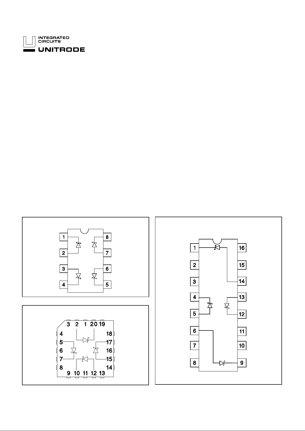
Quad Schottky Diode Array
CONNECTION DIAGRAM
DIL-8 (TOP VIEW)
N or J Package
PLCC-20 (TOP VIEW)
Q Package
SOIC-16 (TOP VIEW )
DW Package
6/93
ABSOLUTE MAXI MUM RATING S
Peak Inverse Voltag e (per Diode). . . . . . . . . . . . . . . . . . . . . . . . . . . . . . . . . 50V
Diode-to-Diode V o ltage. . . . . . . . . . . . . . . . . . . . . . . . . . . . . . . . . . . . . . . . . 80V
Peak Forwar d Curr ent
UC1611. . . . . . . . . . . . . . . . . . . . . . . . . . . . . . . . . . . . . . . . . . . . . . . . . . . . 1A
UC3611. . . . . . . . . . . . . . . . . . . . . . . . . . . . . . . . . . . . . . . . . . . . . . . . . . . . 3A
Power Dissipat ion at T
A = +70°C . . . . . . . . . . . . . . . . . . . . . . . . . . . . . . . . . . 1W
Storage Temperature Range . . . . . . . . . . . . . . . . . . . . . . . . . . -65°C to +150°C
Lead Temperature (Solderin g, 10 Sec onds ). . . . . . . . . . . . . . . . . . . . . . . +300°C
Note: Please consult Packaging Sectio n of Databook for therm al l imitat ions and
considerations of pac kage .
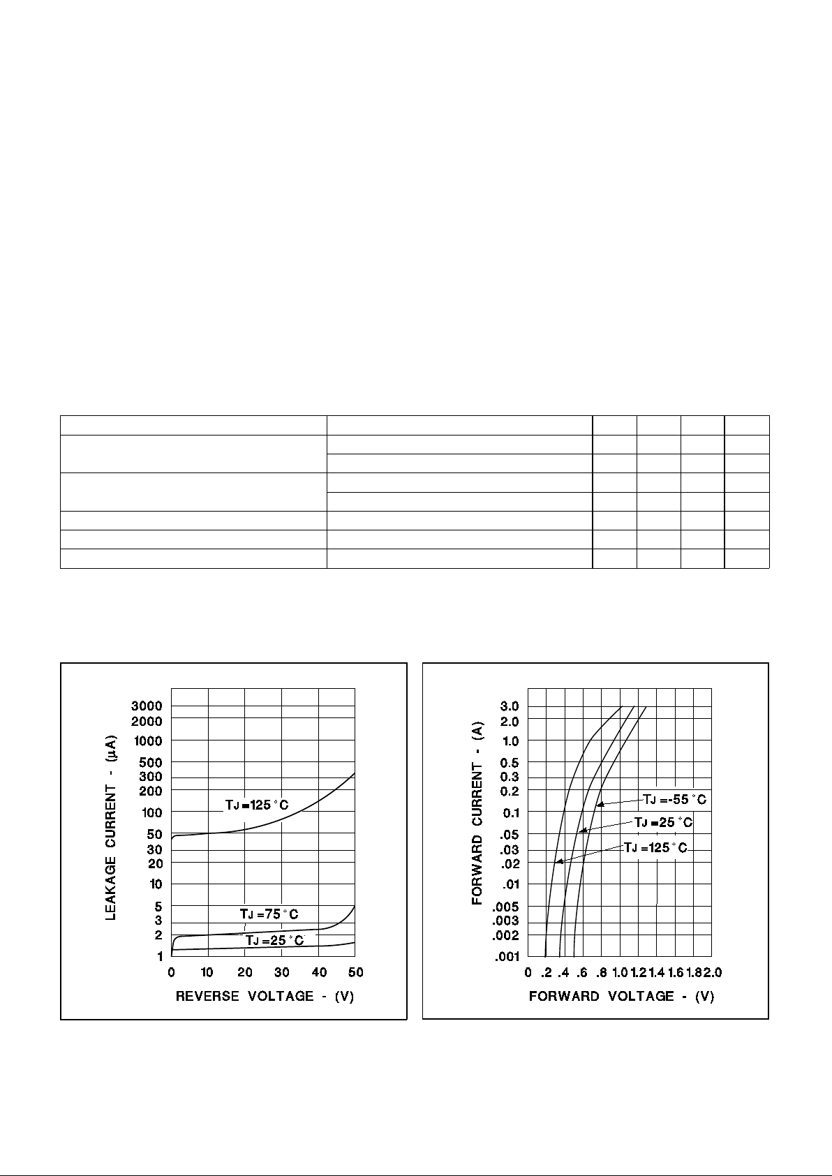
ELECTRICAL CHARACTERISTICS:
PARAMETER TEST CONDITIONS MIN. TYP. MAX. UNITS
Forward Voltage Dro p I
F = 100mA 0.3 0.4 0.7 V
I
F = 1A 0.9 1.2 V
Leakage Current V
R = 40V 0.01 0.1 mA
V
R = 40V, TJ = +100°C 0.1 1.0 mA
Reverse Recovery 0.5A Forward to 0.5A Revers e 20 ns
Forward Recovery 1A Forward to 1.1V Recovery 40 ns
Junction Capacitance V
R = 5V 100 pF
Note: At Forward current s of gr eat er tha n 1.0A, a para sitic cu rrent of appr oxim at ely 10m A may be colle ct ed by adja cent diodes.
All specifications apply to each individual diode . TJ = +25°C except as noted.
TA = TJ.
UC1611
UC3611
Reverse Current vs V oltage Forward Curren t vs Voltage
2

UNITRODE INTEGRATED CIRCUITS
7 CONTINENTAL BLVD. • MERRIMACK, NH 03054
TEL. (603) 424-2410 • FAX (603) 424-3460
UC1611
UC3611
TYPICAL APPLI CATIO NS
C. Li nea r Regulations
B. Tr ansformer Coupled Drive Circuits
A. Clamp Diodes - PWMS and Dr ivers
3

IMPORTANT NOTICE
T exas Instruments and its subsidiaries (TI) reserve the right to make changes to their products or to discontinue
any product or service without notice, and advise customers to obtain the latest version of relevant information
to verify, before placing orders, that information being relied on is current and complete. All products are sold
subject to the terms and conditions of sale supplied at the time of order acknowledgement, including those
pertaining to warranty, patent infringement, and limitation of liability.
TI warrants performance of its semiconductor products to the specifications applicable at the time of sale in
accordance with TI’s standard warranty. Testing and other quality control techniques are utilized to the extent
TI deems necessary to support this warranty. Specific testing of all parameters of each device is not necessarily
performed, except those mandated by government requirements.
CERT AIN APPLICATIONS USING SEMICONDUCTOR PRODUCTS MAY INVOLVE POTENTIAL RISKS OF
DEATH, PERSONAL INJURY, OR SEVERE PROPERTY OR ENVIRONMENTAL DAMAGE (“CRITICAL
APPLICATIONS”). TI SEMICONDUCTOR PRODUCTS ARE NOT DESIGNED, AUTHORIZED, OR
WARRANTED TO BE SUITABLE FOR USE IN LIFE-SUPPORT DEVICES OR SYSTEMS OR OTHER
CRITICAL APPLICATIONS. INCLUSION OF TI PRODUCTS IN SUCH APPLICA TIONS IS UNDERSTOOD T O
BE FULLY AT THE CUSTOMER’S RISK.
In order to minimize risks associated with the customer’s applications, adequate design and operating
safeguards must be provided by the customer to minimize inherent or procedural hazards.
TI assumes no liability for applications assistance or customer product design. TI does not warrant or represent
that any license, either express or implied, is granted under any patent right, copyright, mask work right, or other
intellectual property right of TI covering or relating to any combination, machine, or process in which such
semiconductor products or services might be or are used. TI’s publication of information regarding any third
party’s products or services does not constitute TI’s approval, warranty or endorsement thereof.
Copyright 1999, Texas Instruments Incorporated
 Loading...