

Page 1
uA709C, uA709M, uA709AM
V
max
GENERAL-PURPOSE OPERATIONAL AMPLIFIERS
SLOS096 – D942, FEBRUARY 1971 – REVISED MA Y 1988
• Common-Mode Input Range . . . ±10 V
Typical
• Designed to Be Interchangeable With
Fairchild µA709A, µA709, and µA709C
• Maximum Peak-to-Peak Output Voltage
Swing . . . 28-V Typical With 15-V Supplies
description
These circuits are general-purpose operational
amplifiers, each having high-impedance
differential inputs and a low-impedance output.
Component matching, inherent with silicon
monolithic circuit-fabrication techniques,
produces an amplifier with low-drift and low-offset
characteristics. Provisions are incorporated within
the circuit whereby external components may be
used to compensate the amplifier for stable
operation under various feedback or load
conditions. These amplifiers are particularly
useful for applications requiring transfer or
generation of linear or nonlinear functions.
The uA709A circuit features improved offset
characteristics, reduced input-current
requirements, and lower power dissipation when
compared to the uA709 circuit. In addition,
maximum values of the average temperature
coefficients of offset voltage and current are
specified for the uA709A.
The uA709C is characterized for operation from
0°C to 70°C. The uA709AM and uA709M are
characterized for operation over the full military
temperature range of –55°C to 125°C.
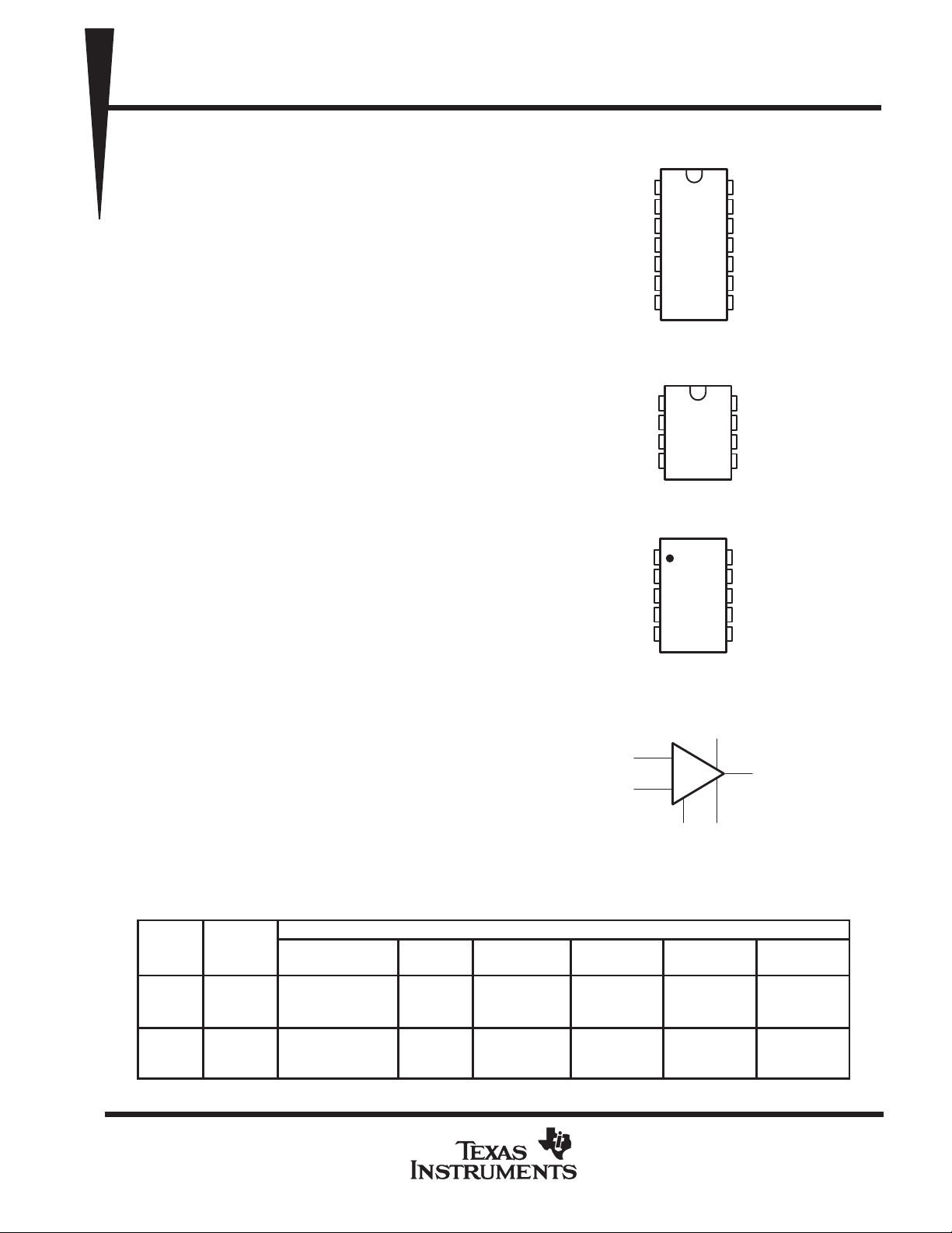
uA709AM, uA709M ...J OR W PACKAGE
FREQ COMP B
V
CC –
uA709AM, uA709M ... JG PACKAGE
uA709C . . . D, JG, OR P PACKAGE
FREQ COMP B
IN –
IN +
V
CC –
uA709AM, uA709M ...U FLAT PACKAGE
FREQ COMP B
V
NC – No internal connection
symbol
IN +
IN –
NC
NC
IN –
IN +
NC
NC
IN –
IN +
CC
(TOP VIEW)
1
14
2
13
3
12
4
11
5
10
6
7
(TOP VIEW)
(TOP VIEW)
1
2
3
4
5
9
8
1
2
3
4
8
7
6
5
10
9
8
7
6
OUT FREQ COMP
+
–
NC
NC
FREQ COMP A
V
CC +
OUT
OUT FREQ COMP
NC
FREQ COMP A
V
CC +
OUT
OUT FREQ COMP
NC
FREQ COMP A
V
CC +
OUT
OUT FREQ COMP
OUT
FREQ
FREQ
COMP
COMP
AVAILABLE OPTIONS
T
A
0°C
to
70°C
–55°C
to
125°C
The D package is available taped and reeled. Add the suffix R to the device type when ordering, (e.g., uA709CDR).
PRODUCTION DATA information is current as of publication date.
Products conform to specifications per the terms of Texas Instruments
standard warranty. Production processing does not necessarily include
testing of all parameters.
IO
AT 25°C
7.5 mV uA709CD — uA709CJG uA709CP — —
5 mV
2 mV
SMALL OUTLINE
(D)
—
CERAMIC
(J)
uA709MJ
uA709AMJ
POST OFFICE BOX 655303 • DALLAS, TEXAS 75265
CERAMIC DIP
PACKAGE
(JG)
uA709MJG
uA709AMJG
PLASTIC DIP
(P)
—
Copyright 1988, Texas Instruments Incorporated
BA
FLAT PACK
(U)
uA709MU
uA709AMU
FLAT PACK
(W)
uA709MW
uA709AMW
1
Page 2
uA709C, uA709M, uA709AM
A709C
UNIT
GENERAL-PURPOSE OPERATIONAL AMPLIFIERS
SLOS096 – D942, FEBRUARY 1971 – REVISED MAY 1988
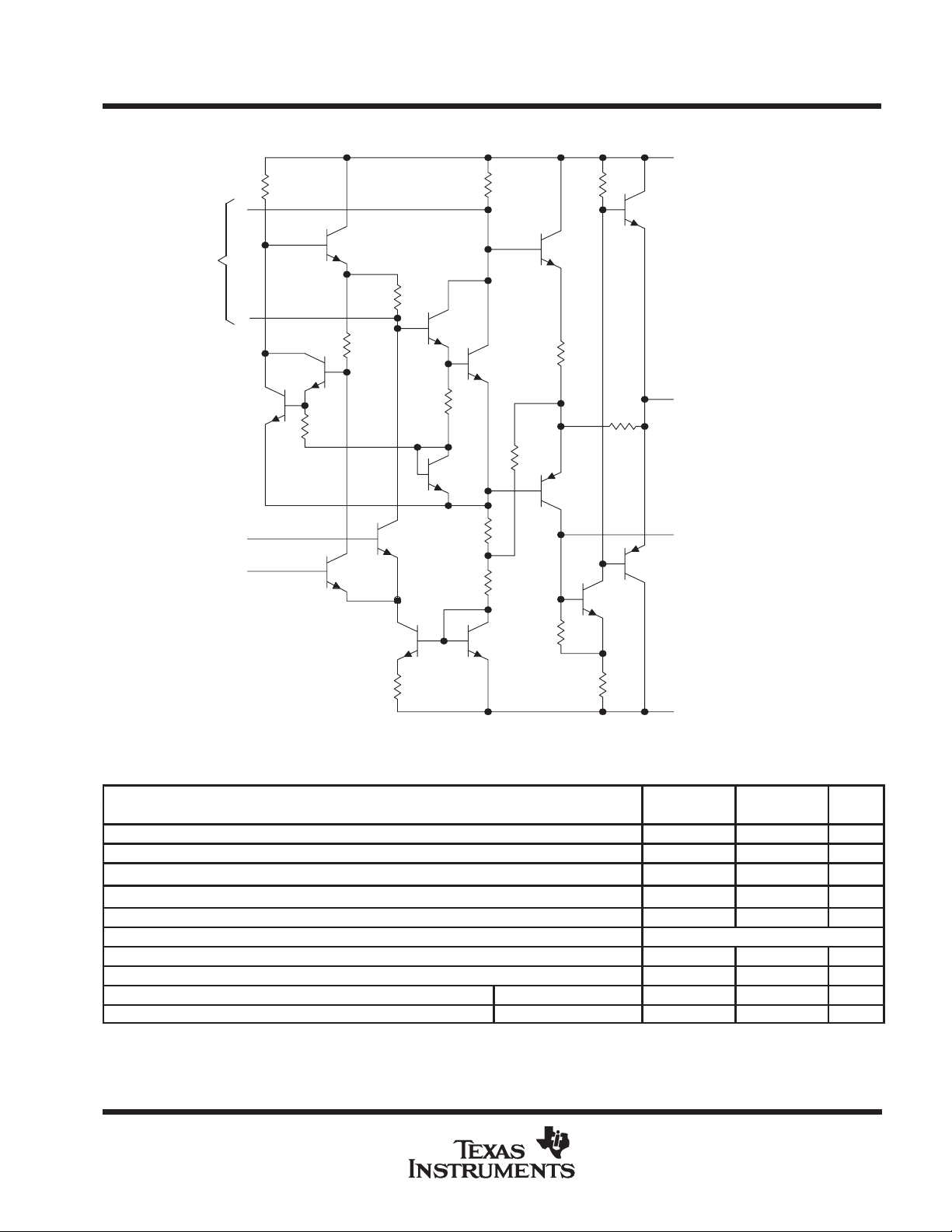
schematic
10 kΩ 10 kΩ
A
FREQ
COMP
25 kΩ
B
20 kΩ
V
CC +
3 kΩ
IN –
IN +
Component values shown are nominal.
25 kΩ
3 kΩ
10 kΩ
3.6 kΩ
18 kΩ
2.4 kΩ
1 kΩ
10 kΩ
75 kΩ
30 kΩ
OUT
OUT FREQ COMP
V
CC –
absolute maximum ratings over operating free-air temperature range (unless otherwise noted)
u
Supply voltage, V
Supply voltage, V
Differential input voltage (see Note 2) ±5
Input voltage (either input, see Notes 1 and 3) ±10
Duration of output short circuit (see Note 4) 5 5 s
Continuous total power dissipation See Dissipation Rating Table
Operating free-air temperature range 0 to 70 –55 to 125 ° C
Storage temperature range –65 to 150 –65 to 150 ° C
Lead temperature 1,6 mm (1/16 inch) from case for 60 seconds J, JG, U, or W package 300 300 °C
Lead temperature 1,6 mm (1/16 inch) from case for 10 seconds D or P package 260 °C
NOTES: 1. All voltage values, unless otherwise noted, are with respect to the midpoint between V
2. Differential voltages are at the noninverting input terminal with respect to the inverting input terminal.
3. The magnitude of the input voltage must never exceed the magnitude of the supply voltage or 10 V, whichever is less.
4. The output may be shorted to ground or either power supply .
(see Note 1) 18 18 V
CC+
(see Note 1) –18 –18 V
CC–
and V
CC+
CC–
uA709AM
.
uA709M
±5
±10
V
V
2
POST OFFICE BOX 655303 • DALLAS, TEXAS 75265
Page 3

uA709C, uA709M, uA709AM
GENERAL-PURPOSE OPERATIONAL AMPLIFIERS
SLOS096 – D942, FEBRUARY 1971 – REVISED MAY 1988
DISSIPATION RATING TABLE
PACKAGE
D 300 mW N/A N/A 300 mW N/A
J (uA709_M) 300 mW 11.0 mW/°C 123°C 300 mW 275 mW
JG (uA709_M) 300 mW 8.4 mW/°C114°C 300 mW 210 mW
JG (uA709C) 300 mW N/A N/A 300 mW N/A
P 300 mW N/A N/A 300 mW N/A
U 300 mW 5.4 mW/°C94°C 300 mW 135 mW
W 300 mW 8.0 mW/°C 113°C 300 mW 200 mW
TA ≤ 25°C
POWER RATING
DERATING
FACTOR
DERATE
ABOVE T
TA = 70°C
POWER RATING
A
TA = 125°C
POWER RATING
POST OFFICE BOX 655303 • DALLAS, TEXAS 75265
3
Page 4

uA709M, uA709AM
PARAMETER
TEST CONDITIONS
†
T
‡
UNIT
VIOInput offset voltage
V
R
kΩ
V
R
Ω
Full range
1.8103
coefficient of input
V/°C
offset voltage
V
0
R
10 kΩ
Full range
4.8256
0.45
2.8
coefficient of input
V
0
nA/°C
offset voltage
0.08
0.5
IIBInput bias current
V
0
A
V
V
±15 V
V
V
±15 V
R
kΩ
V
V
A
gg
CC± L
V/mV
riInput resistance
kΩ
CMRR
V
V
min
dB
k
yy
V
V
V/V
V
V
O
0
V
±15 V
load
V
O
0
GENERAL-PURPOSE OPERATIONAL AMPLIFIERS
SLOS096 – D942, FEBRUARY 1971 – REVISED MAY 1988
electrical characteristics at specified free-air temperature, V
= ± 9 V to ± 15 V (unless otherwise
±
CC
noted)
A
p
Average temperature
α
VIO
I
IO
α
VIO
ICR
O(PP)
VD
r
o
SVS
I
CC
P
D
†
All characteristics are specified under open-loop with zero common-mode input voltage unless otherwise specified.
‡
Full range for uA709C is 0°C to 70°C. Full range for uA709AM and uA709M is –55°C to 125°C.
§
All typical values are at V
NOTE 5: This typical value applies only at frequencies above a few hundred hertz because of the effects of drift and thermal feedback.
Input offset current VO = 0 –55°C 40 250 100 500 nA
Average temperature
p
Common-mode
input voltage range
Maximum peak-to-peak
output voltage swing
Large-signal differential V
voltage amplification
p
Output resistance VO = 0, See Note 5 25°C 150 150 Ω
Common-mode
rejection ratio
Power supply sensitivity
(∆VIO / ∆VCC)
Supply current
Total power dissipation
p
p
CC±
= ±15 V .
= 0,
O
= 0,
O
,
=
O
=
O
=
O
=
CC±
=
CC±
V
= ±15 V, RL = 2 kΩ
CC±
V
= ±15 V, RL ≥ 2 kΩ Full range 20 20
CC±
= ±15 V, RL ≥ 2 kΩ,
CC±
VO = ± 10 V
=
IC
ICR
= ± 9 V to ± 15
CC
= ±15 V, No load,
CC±
=
=
CC±
=
=
,
, No
S
S
S
≥ 10
L
≤ 10
= 50
=
,
25°C 0.6 2 1 5 mV
Full range 3 6
25°C 10 50 50 200
125°C 3.5 50 20 200
–55°C to
25°C
25°C to
125°C
25°C 0.1 0.2 0.2 0.5
–55°C 0.3 0.6 0.5 1.5
25°C ±8 ±10 ±8 ±10
Full range ±8 ±8
25°C 24 28 24 28
Full range 24 24
25°C 20 26 20 26
25°C 45 45
Full range 25 70 25 70
25°C 350 750 150 400
–55°C 85 185 40 100
25°C 80 110 70 90
Full range 80 70
25°C 40 100 25 150
Full range 100 150
25°C 2.5 3.6 2.6 5.5
–55°C 2.7 4.5 mA
125°C 2.1 3
25°C 75 108 78 165
–55°C 81 135 mW
125°C 63 90
uA709AMC uA709M
MIN TYP§MAX MIN TYP§MAX
°
µ
°
µ
µ
4
POST OFFICE BOX 655303 • DALLAS, TEXAS 75265
Page 5

uA709C, uA709M, uA709AM
PARAMETER
TEST CONDITIONS
†
T
‡
UNIT
VIOInput offset voltage
V
±15 V, V
0
mV
IIOInput offset current
V
±15 V, V
0
nA
IIBInput bias current
V
±15 V, V
0
A
R
kΩ
V
V
R
V
V
V/mV
riInput resistance
kΩ
A709M
PARAMETER
TEST CONDITIONS
†
UNIT
V
I
R
L
See Figure 1
GENERAL-PURPOSE OPERATIONAL AMPLIFIERS
SLOS096 – D942, FEBRUARY 1971 – REVISED MAY 1988
electrical characteristics at specified free-air temperature (unless otherwise noted V
A
p
p
p
V
ICR
O(PP)
A
VD
r
o
CMRR Common-mode rejection ratio VIC = V
k
SVS
P
D
†
All characteristics are specified under open-loop operation with zero volts common-mode voltage unless otherwise specified.
‡
Full range for uA709C is 0°C to 70°C. Full range for uA709AM and uA709M is –55°C to 125°C.
NOTE 5: This typical value applies only at frequencies above a few hundred hertz because of the effects of drift and thermal feedback.
Common-mode input voltage range 25°C ±8 ±10 V
Maximum peak-to-peak
output voltage swing
Large-signal differential
voltage amplification
p
Output resistance VO = 0, See Note 5 25°C 150 Ω
Supply voltage sensitivity VCC = ±9 V to ±15 V 25°C 25 200 µV/V
Total power dissipation VO = 0, No load 25°C 80 200 mW
= ±9 V to
CC±
= ±9 V to
CC±
= ±9 V to
CC±
≥ 10
L
RL = 2 kΩ
RL ≥ 2 kΩ Full range 20
≤ 2 kΩ,
L
min 25°C 65 90 dB
ICR
= ± 10
O
=
O
=
O
=
O
25°C 2 7.5
Full range 10
25°C 100 500
Full range 750
25°C 0.3 1.5
Full range 2
25°C 24 28
Full range 24
25°C 20 26
25°C 15 45
Full range 12
25°C 50 250
Full range 35
uA709C
MIN TYP MAX
CC
= ± 15 V)
±
µ
operating characteristics, V
t
r
Rise time
Overshoot factor
PARAMETER MEASUREMENT INFORMATION
V
I
0 V
INPUT VOLTAGE
WAVEFORM
= ± 9 V to ± 15 V, TA = 25°C
±
CC
= 20 mV,
Input
= 2 kΩ,
10 kΩ
100 pF
COMP B
5000 pF
–
+
10 kΩ
200 pF
OUT
FREQ
COMP
COMP A
1.5 kΩ
uA709C
u
uA709AM
MIN TYP MAX
CL = 0 0.3 1 µs
CL = 100 pF 6% 30%
50 kΩ
CL = 100 pF
RL = 2 kΩ
FREQFREQ
Output
Figure 1. Rise Time and Slew Rate Test Circuit
POST OFFICE BOX 655303 • DALLAS, TEXAS 75265
5
Page 6

IMPORTANT NOTICE
T exas Instruments and its subsidiaries (TI) reserve the right to make changes to their products or to discontinue
any product or service without notice, and advise customers to obtain the latest version of relevant information
to verify, before placing orders, that information being relied on is current and complete. All products are sold
subject to the terms and conditions of sale supplied at the time of order acknowledgement, including those
pertaining to warranty, patent infringement, and limitation of liability.
TI warrants performance of its semiconductor products to the specifications applicable at the time of sale in
accordance with TI’s standard warranty. Testing and other quality control techniques are utilized to the extent
TI deems necessary to support this warranty . Specific testing of all parameters of each device is not necessarily
performed, except those mandated by government requirements.
CERT AIN APPLICATIONS USING SEMICONDUCTOR PRODUCTS MAY INVOLVE POTENTIAL RISKS OF
DEATH, PERSONAL INJURY, OR SEVERE PROPERTY OR ENVIRONMENTAL DAMAGE (“CRITICAL
APPLICATIONS”). TI SEMICONDUCTOR PRODUCTS ARE NOT DESIGNED, AUTHORIZED, OR
WARRANTED TO BE SUITABLE FOR USE IN LIFE-SUPPORT DEVICES OR SYSTEMS OR OTHER
CRITICAL APPLICA TIONS. INCLUSION OF TI PRODUCTS IN SUCH APPLICATIONS IS UNDERST OOD TO
BE FULLY AT THE CUSTOMER’S RISK.
In order to minimize risks associated with the customer’s applications, adequate design and operating
safeguards must be provided by the customer to minimize inherent or procedural hazards.
TI assumes no liability for applications assistance or customer product design. TI does not warrant or represent
that any license, either express or implied, is granted under any patent right, copyright, mask work right, or other
intellectual property right of TI covering or relating to any combination, machine, or process in which such
semiconductor products or services might be or are used. TI’s publication of information regarding any third
party’s products or services does not constitute TI’s approval, warranty or endorsement thereof.
Copyright 1998, Texas Instruments Incorporated
 Loading...