

Texas Instruments TVS 0 Series, TVS140 Series, TVS180 Series, TVS220 Series, TVS270 Series User Manual
...Page 1
User's Guide
SLVUBJ8–October 2018
Flat Clamp TVS Evaluation Module—Adaptor Boards
This user's guide describes the characteristics, operation, and use of the TVSxx0x Precision Surge
Protection Diode Adaptor Board Evaluation Module (EVM). The TVSxx0x family of devices are precision
clamps that keep ultra-low and flat clamping voltages during transient overvoltage events like surge for
both bidirectional and unidirectional signals. These adaptor boards place the small DRV package size of
the TVSxx00 device and the small DRB package size of the TVSxx01 device into a larger footprint that is
designed to fit into industry standard SMA and SMB package types and allow users to test performance in
their own systems. This user's guide includes setup instructions, schematic diagrams, a bill of materials,
and printed-circuit board layout drawings for the EVM.
Contents
1 Introduction ................................................................................................................... 2
2 Board Setup .................................................................................................................. 2
2.1 Surge Testing ....................................................................................................... 3
2.2 ESD Testing ......................................................................................................... 4
3 Schematic..................................................................................................................... 5
4 Layout ......................................................................................................................... 9
5 Bill of Materials ............................................................................................................. 10
1 Unidirectional Adapter Board............................................................................................... 2
2 Bidirectional Adapter Board ................................................................................................ 2
3 Surge Test Setup Unidirectional Configuration.......................................................................... 3
4 TVS3300 35-A Surge Clamping Waveforms............................................................................. 3
5 FLAT-CLAMP-TVS-EVM Board ........................................................................................... 4
6 TVS0500 Schematic......................................................................................................... 5
7 TVS0701 Schematic......................................................................................................... 5
8 TVS140X Schematic ........................................................................................................ 5
9 TVS180X Schematic ........................................................................................................ 5
10 TVS220X Schematic ........................................................................................................ 6
11 TVS270X Schematic ........................................................................................................ 6
12 TVS330X Schematic ........................................................................................................ 7
13 Evaluation Module Top Layer.............................................................................................. 9
14 Evaluation Module Bottom Layer .......................................................................................... 9
1 Evaluation Module Bill of Materials ...................................................................................... 10
Trademarks
All trademarks are the property of their respective owners.
List of Figures
List of Tables
SLVUBJ8–October 2018
Submit Documentation Feedback
Flat Clamp TVS Evaluation Module—Adaptor Boards
Copyright © 2018, Texas Instruments Incorporated
1
Page 2
200 mil
(5mm)
SOLDER
SOLDER
Bidirectional
Adapter Board
145 mil
(3.7mm)
50 mil
(1.27mm)
200 mil
(5mm)
SOLDERSOLDER
Unidirectional
Adapter Board
105 mil
(2.6mm)
55 mil
(1.4mm)
85 mil
(2.16mm)
Introduction
1 Introduction
Texas Instrument’s TVSxx0x evaluation module helps designers evaluate the operation and performance
of the TVSxx0x family of devices. The TVSxx0x family is a precision clamp that keeps ultra-low and flat
clamping voltage during transient overvoltage events like surge. With TI’s precision surge technology, the
TVSxx0x's clamping voltage barely changes up to its maximum surge current. The TVSxx0x also
responds fast to the surge to limit overshoot voltage during clamping. Used in the system, its superior
voltage suppression performance ensures a safe environment for downstream protected circuits.
2 Board Setup
The Flat Clamp Adaptor Board EVM is designed to allow the user to evaluate the protection performance
of the TVSxx0x in their own system without having to make any changes to their existing schematic or
layout. The EVM serves as an adaptor board to allow the small size of the QFN chip to be placed pin for
pin in the industry standard SMA and SMB surge protector footprints. Users can easily replace their
existing surge solution chip with the TVS3300 EVM to evaluate the component.
This EVM kit contains 36 adapter boards with 6 boards for each of the TVSxx0x voltage levels. 3 adapter
boards per voltage level are in unidirectional configuration and 3 adapter boards per voltage level are in
bidirectional configuration. Based on their system, the user must use the unidirectional configuration if the
signal on the protected line stays above 0 V. Otherwise, it is recommended to use the bidirectional
configuration, which can protect the system if the signal contains both positive and negative voltages.
The unidirectional adapter boards are all 105mil x 200mil (2.6mm x 5mm) and the bidirectional adapter
boards are 145mil by 200mil (3.7mm x 5mm). The solderable pad underneath each adapter board is 85mil
x 55mil for the unidirectional and 145mil x 50mil for the bidirectional. This can be seen in the figures
below.
www.ti.com
2
Figure 1. Unidirectional Adapter Board
Figure 2. Bidirectional Adapter Board
Flat Clamp TVS Evaluation Module—Adaptor Boards
Copyright © 2018, Texas Instruments Incorporated
SLVUBJ8–October 2018
Submit Documentation Feedback
Page 3
Time (Ps)
Amplitude (V or A)
-20 -10 0 10 20 30 40 50 60 70 80
0
4
8
12
16
20
24
28
32
36
40
D006
Voltage (V)
Current (A)
www.ti.com
To install the EVM, remove the existing surge protection solution, cut out the adapter board needed for
your applications and place the adaptor board in the existing footprint. If there is no existing surge
protection solution in the system, the EVM can still be tested by soldering the bottom plates of the adaptor
board over the protected line and a ground plane. In the unidirectional configuration, pin 1 of the adapter
board must be installed pointing towards ground, pin 1 can be seen by the silkscreen bar on one side of
the unidirectional adaptor boards. In the bidirectional configuration either pin can be connected to ground
or input signal. Each adapter board has solder pads on the bottom extending to the edge allowing the
board to be soldered down.
2.1 Surge Testing
The adaptor provides an easy way to test the TVSxx0x surge protection as defined in IEC 61000-4-5.
Evaluate the TVSxx0x surge protection by exposing the protected line to a surge event. The event must
be created by a combinational waveform generator (CWG) in series with a 40-Ω coupling resistor as
shown in Figure 3. Test at different surge current levels and observe that the voltage on the line is
clamped to a safe level for the protected system. After the surge event, post-test the system to ensure that
no damage or shift in leakage currents occurred.
Board Setup
Figure 3. Surge Test Setup Unidirectional Configuration
The waveform in Figure 4 shows the response of the TVSxx0x Unidirectional adaptor board to a 30-A
surge waveform created by a similar setup as in Figure 3. Despite the 35 A of current over a IEC 61000-45 surge waveform, the TVS3300 holds the voltage on the line to a maximum of 37 V, robustly protecting
the downstream components.
Figure 4. TVS3300 35-A Surge Clamping Waveforms
This is just one of the 6 different voltage level devices on the adapter board with all of them having
superior clamping for their node.
SLVUBJ8–October 2018
Submit Documentation Feedback
Flat Clamp TVS Evaluation Module—Adaptor Boards
Copyright © 2018, Texas Instruments Incorporated
3
Page 4
Board Setup
2.2 ESD Testing
The TVSxx0x devices also provides ESD protection above ±8-kV contact and ±15-kV air gap according to
the IEC 61000-4-2 standard. After installing the adaptor board into the system, evaluate the ESD
protection provided by the TVSxx0x by using an ESD simulator to create an ESD event on your protected
line. For specific information on ESD testing procedures, see the application report, IEC 61000-4-x Tests
for TI’s Protection Devices.
Figure 5 shows all the adapter boards that come in one evaluation module.
www.ti.com
Figure 5. FLAT-CLAMP-TVS-EVM Board
4
Flat Clamp TVS Evaluation Module—Adaptor Boards
Copyright © 2018, Texas Instruments Incorporated
SLVUBJ8–October 2018
Submit Documentation Feedback
Page 5
GND3
Protected Line3
Protected Line5
GND5
Protected Line7
GND7
IN
1
IN
2
IN
3
IN
4
GND
5
GND
6
GND
7
GND
8
NC
9
TVS0701DRBR
U4
IN
1
IN
2
IN
3
IN
4
GND
5
GND
6
GND
7
GND
8
NC
9
TVS0701DRBR
U5
IN
1
IN
2
IN
3
IN
4
GND
5
GND
6
GND
7
GND
8
NC
9
TVS0701DRBR
U6
GND
Protected Line
IN
4
IN
5
GND
1
GND
2
IN
6
GND
3
PAD
7
U1
TVS0500DRVR
GND1
Protected Line1
GND2
Protected Line2
IN
4
IN
5
GND
1
GND
2
IN
6
GND
3
PAD
7
U2
TVS0500DRVR
IN
4
IN
5
GND
1
GND
2
IN
6
GND
3
PAD
7
U3
TVS0500DRVR
www.ti.com
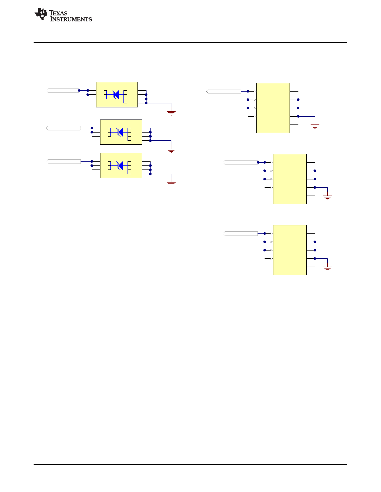
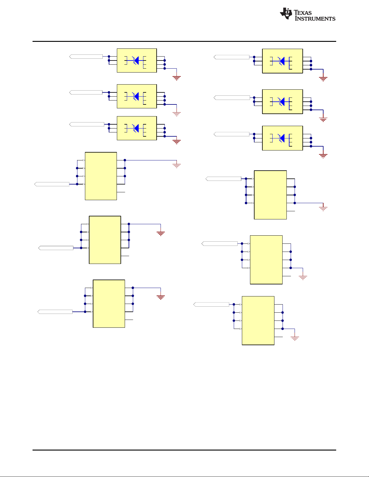
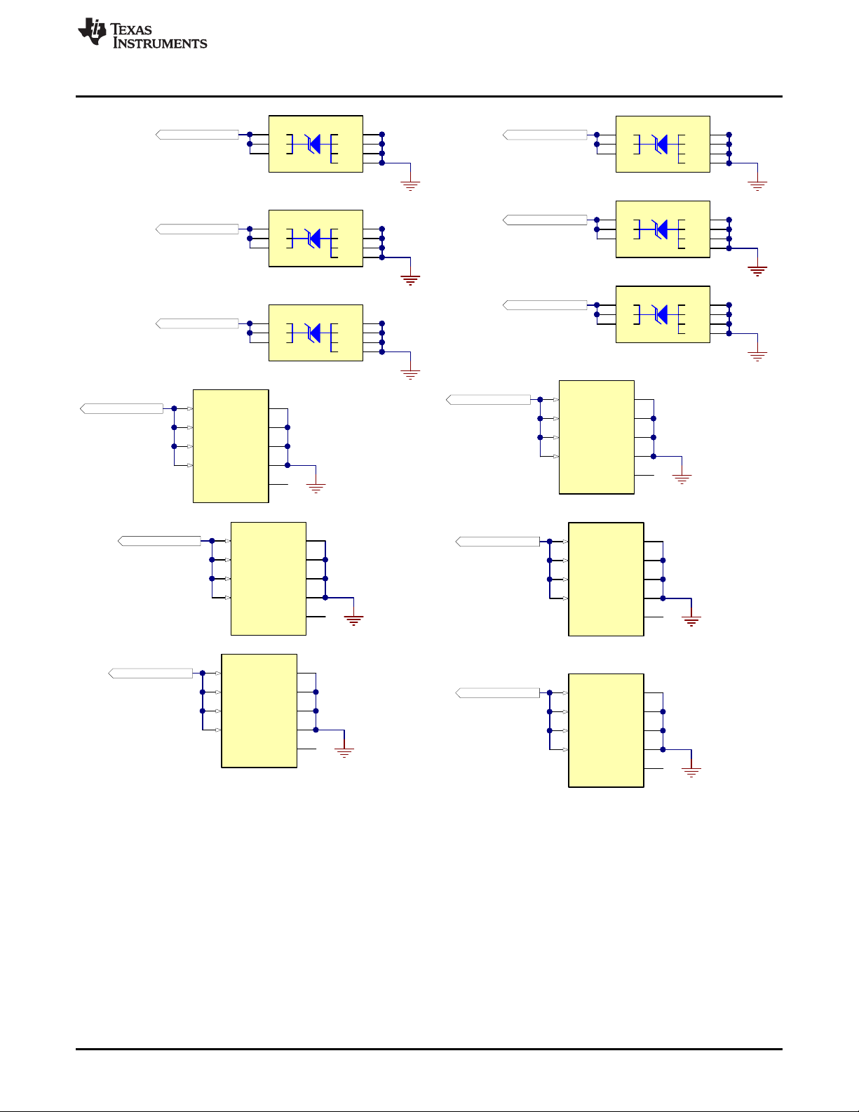
3 Schematic
Figure 6 through Figure 12 display the EVM schematics with each voltage node.
Schematic
Figure 6. TVS0500 Schematic Figure 7. TVS0701 Schematic
SLVUBJ8–October 2018
Submit Documentation Feedback
Flat Clamp TVS Evaluation Module—Adaptor Boards
Copyright © 2018, Texas Instruments Incorporated
5
Page 6
IN
4
IN
5
GND
1
GND
2
IN
6
GND
3
PAD
7
U13
TVS1800DRVR
GND14
Protected Line14
IN
4
IN
5
GND
1
GND
2
IN
6
GND
3
PAD
7
U14
TVS1800DRVR
GND15
Protected Line15
IN
4
IN
5
GND
1
GND
2
IN
6
GND
3
PAD
7
U15
TVS1800DRVR
GND16
Protected Line16
GND17
Protected Line17
GND18
GND19
Protected Line18
Protected Line19
IN
1
IN
2
IN
3
IN
4
GND
5
GND
6
GND
7
GND
8
NC
9
TVS1801DRBR
U16
IN
1
IN
2
IN
3
IN
4
GND
5
GND
6
GND
7
GND
8
NC
9
TVS1801DRBR
U17
IN
1
IN
2
IN
3
IN
4
GND
5
GND
6
GND
7
GND
8
NC
9
TVS1801DRBR
U18
IN
4
IN
5
GND
1
GND
2
IN
6
GND
3
PAD
7
U7
TVS1400DRVR
Protected Line8
GND8
IN
4
IN
5
GND
1
GND
2
IN
6
GND
3
PAD
7
U8
TVS1400DRVR
Protected Line9
GND9
IN
4
IN
5
GND
1
GND
2
IN
6
GND
3
PAD
7
U9
TVS1400DRVR
Protected Line10
GND10
GND12
GND13
Protected Line13
Protected Line12
GND11
Protected Line11
IN
1
IN
2
IN
3
IN
4
GND
5
GND
6
GND
7
GND
8
NC
9
TVS1401DRBR
U10
IN
1
IN
2
IN
3
IN
4
GND
5
GND
6
GND
7
GND
8
NC
9
TVS1401DRBR
U11
IN
1
IN
2
IN
3
IN
4
GND
5
GND
6
GND
7
GND
8
NC
9
TVS1401DRBR
U12
Schematic
6
Flat Clamp TVS Evaluation Module—Adaptor Boards
Figure 8. TVS140X Schematic Figure 9. TVS180X Schematic
Copyright © 2018, Texas Instruments Incorporated
www.ti.com
SLVUBJ8–October 2018
Submit Documentation Feedback
Page 7
Protected Line26
GND26
IN
4
IN
5
GND
1
GND
2
IN
6
GND
3
PAD
7
U26
TVS2700DRVR
Protected Line27
GND27
IN
4
IN
5
GND
1
GND
2
IN
6
GND
3
PAD
7
U27
TVS2700DRVR
Protected Line28
GND28
Protected Line29
GND29
Protected Line30
GND30
Protected Line31
GND31
IN
4
IN
5
GND
1
GND
2
IN
6
GND
3
PAD
7
U25
TVS2700DRVR
IN
1
IN
2
IN
3
IN
4
GND
5
GND
6
GND
7
GND
8
NC
9
TVS2701DRBR
U28
IN
1
IN
2
IN
3
IN
4
GND
5
GND
6
GND
7
GND
8
NC
9
TVS2701DRBR
U29
IN
1
IN
2
IN
3
IN
4
GND
5
GND
6
GND
7
GND
8
NC
9
TVS2701DRBR
U30
IN
4
IN
5
GND
1
GND
2
IN
6
GND
3
PAD
7
U19
TVS2200DRVR
IN
4
IN
5
GND
1
GND
2
IN
6
GND
3
PAD
7
U20
TVS2200DRVR
IN
4
IN
5
GND
1
GND
2
IN
6
GND
3
PAD
7
U21
TVS2200DRVR
Protected Line20
Protected Line21
Protected Line22
GND20
GND21
GND22
Protected Line23
GND23
Protected Line24
GND24
Protected Line25
GND25
IN
1
IN
2
IN
3
IN
4
GND
5
GND
6
GND
7
GND
8
NC
9
TVS2201DRBR
U22
IN
1
IN
2
IN
3
IN
4
GND
5
GND
6
GND
7
GND
8
NC
9
TVS2201DRBR
U23
IN
1
IN
2
IN
3
IN
4
GND
5
GND
6
GND
7
GND
8
NC
9
TVS2201DRBR
U24
www.ti.com
SLVUBJ8–October 2018
Submit Documentation Feedback
Figure 10. TVS220X Schematic Figure 11. TVS270X Schematic
Flat Clamp TVS Evaluation Module—Adaptor Boards
Copyright © 2018, Texas Instruments Incorporated
Schematic
7
Page 8

IN
4
IN
5
GND
1
GND
2
IN
6
GND
3
PAD
7
U31
TVS3300DRVR
IN
4
IN
5
GND
1
GND
2
IN
6
GND
3
PAD
7
U32
TVS3300DRVR
IN
4
IN
5
GND
1
GND
2
IN
6
GND
3
PAD
7
U33
TVS3300DRVR
Protected Line32
Protected Line33
Protected Line34
Protected Line35
Protected Line36
Protected Line37
GND32
GND33
GND34
GND35
GND36
GND37
IN
1
IN
2
IN
3
IN
4
GND
5
GND
6
GND
7
GND
8
NC
9
TVS3301DRBR
U34
IN
1
IN
2
IN
3
IN
4
GND
5
GND
6
GND
7
GND
8
NC
9
TVS3301DRBR
U35
IN
1
IN
2
IN
3
IN
4
GND
5
GND
6
GND
7
GND
8
NC
9
TVS3301DRBR
U36
Schematic
www.ti.com
Figure 12. TVS330X Schematic
8
Flat Clamp TVS Evaluation Module—Adaptor Boards
Copyright © 2018, Texas Instruments Incorporated
SLVUBJ8–October 2018
Submit Documentation Feedback
Page 9

www.ti.com
4 Layout
Figure 13 and Figure 14 illustrate the PCB layout images.
Layout
Figure 13. Evaluation Module Top Layer
Figure 14. Evaluation Module Bottom Layer
SLVUBJ8–October 2018
Submit Documentation Feedback
Flat Clamp TVS Evaluation Module—Adaptor Boards
Copyright © 2018, Texas Instruments Incorporated
9
Page 10

Bill of Materials
5 Bill of Materials
Designator QtY Value Description Package
U1,U2,U3,U4
,U5,U6,U7,U
8,U9
U10,U11,U1
2,U13,U14,U
15,U16,U17,
U18
U19,U20,U2
1,U22,U23,U
24,U25,U26,
U27,
U28,U29,U3
0,U31,U32,U
33,U34,U35,
U36
U37,U38,U3
9,U40,U41,U
42,U43,U44,
U45
U46,U47,U4
8,U49,U50,U
51,U52,U53,
U54
9 5 V 5-V Precision Surge Protection Clamp DRV TVS0500DRV Texas Instruments
9 14 V 14-V Precision Surge Protection Clamp DRV TVS1400DRV Texas Instruments
9 18 V 18-V Precision Surge Protection Clamp DRV TVS1800DRV Texas Instruments
9 22 V 22-V Precision Surge Protection Clamp DRV TVS2200DRV Texas Instruments
9 27 V 27-V Precision Surge Protection Clamp DRV TVS2700DRV Texas Instruments
9 33 V 33-V Precision Surge Protection Clamp DRV TVS3300DRV Texas Instruments
www.ti.com
Table 1. Evaluation Module Bill of Materials
Part Number Manufacturer
Reference
10
Flat Clamp TVS Evaluation Module—Adaptor Boards
Copyright © 2018, Texas Instruments Incorporated
SLVUBJ8–October 2018
Submit Documentation Feedback
Page 11

STANDARD TERMS FOR EVALUATION MODULES
1. Delivery: TI delivers TI evaluation boards, kits, or modules, including any accompanying demonstration software, components, and/or
documentation which may be provided together or separately (collectively, an “EVM” or “EVMs”) to the User (“User”) in accordance
with the terms set forth herein. User's acceptance of the EVM is expressly subject to the following terms.
1.1 EVMs are intended solely for product or software developers for use in a research and development setting to facilitate feasibility
evaluation, experimentation, or scientific analysis of TI semiconductors products. EVMs have no direct function and are not
finished products. EVMs shall not be directly or indirectly assembled as a part or subassembly in any finished product. For
clarification, any software or software tools provided with the EVM (“Software”) shall not be subject to the terms and conditions
set forth herein but rather shall be subject to the applicable terms that accompany such Software
1.2 EVMs are not intended for consumer or household use. EVMs may not be sold, sublicensed, leased, rented, loaned, assigned,
or otherwise distributed for commercial purposes by Users, in whole or in part, or used in any finished product or production
system.
2 Limited Warranty and Related Remedies/Disclaimers:
2.1 These terms do not apply to Software. The warranty, if any, for Software is covered in the applicable Software License
Agreement.
2.2 TI warrants that the TI EVM will conform to TI's published specifications for ninety (90) days after the date TI delivers such EVM
to User. Notwithstanding the foregoing, TI shall not be liable for a nonconforming EVM if (a) the nonconformity was caused by
neglect, misuse or mistreatment by an entity other than TI, including improper installation or testing, or for any EVMs that have
been altered or modified in any way by an entity other than TI, (b) the nonconformity resulted from User's design, specifications
or instructions for such EVMs or improper system design, or (c) User has not paid on time. Testing and other quality control
techniques are used to the extent TI deems necessary. TI does not test all parameters of each EVM.
User's claims against TI under this Section 2 are void if User fails to notify TI of any apparent defects in the EVMs within ten (10)
business days after delivery, or of any hidden defects with ten (10) business days after the defect has been detected.
2.3 TI's sole liability shall be at its option to repair or replace EVMs that fail to conform to the warranty set forth above, or credit
User's account for such EVM. TI's liability under this warranty shall be limited to EVMs that are returned during the warranty
period to the address designated by TI and that are determined by TI not to conform to such warranty. If TI elects to repair or
replace such EVM, TI shall have a reasonable time to repair such EVM or provide replacements. Repaired EVMs shall be
warranted for the remainder of the original warranty period. Replaced EVMs shall be warranted for a new full ninety (90) day
warranty period.
3 Regulatory Notices:
3.1 United States
3.1.1 Notice applicable to EVMs not FCC-Approved:
FCC NOTICE: This kit is designed to allow product developers to evaluate electronic components, circuitry, or software
associated with the kit to determine whether to incorporate such items in a finished product and software developers to write
software applications for use with the end product. This kit is not a finished product and when assembled may not be resold or
otherwise marketed unless all required FCC equipment authorizations are first obtained. Operation is subject to the condition
that this product not cause harmful interference to licensed radio stations and that this product accept harmful interference.
Unless the assembled kit is designed to operate under part 15, part 18 or part 95 of this chapter, the operator of the kit must
operate under the authority of an FCC license holder or must secure an experimental authorization under part 5 of this chapter.
3.1.2 For EVMs annotated as FCC – FEDERAL COMMUNICATIONS COMMISSION Part 15 Compliant:
CAUTION
This device complies with part 15 of the FCC Rules. Operation is subject to the following two conditions: (1) This device may not
cause harmful interference, and (2) this device must accept any interference received, including interference that may cause
undesired operation.
Changes or modifications not expressly approved by the party responsible for compliance could void the user's authority to
operate the equipment.
FCC Interference Statement for Class A EVM devices
NOTE: This equipment has been tested and found to comply with the limits for a Class A digital device, pursuant to part 15 of
the FCC Rules. These limits are designed to provide reasonable protection against harmful interference when the equipment is
operated in a commercial environment. This equipment generates, uses, and can radiate radio frequency energy and, if not
installed and used in accordance with the instruction manual, may cause harmful interference to radio communications.
Operation of this equipment in a residential area is likely to cause harmful interference in which case the user will be required to
correct the interference at his own expense.
Page 12

FCC Interference Statement for Class B EVM devices
NOTE: This equipment has been tested and found to comply with the limits for a Class B digital device, pursuant to part 15 of
the FCC Rules. These limits are designed to provide reasonable protection against harmful interference in a residential
installation. This equipment generates, uses and can radiate radio frequency energy and, if not installed and used in accordance
with the instructions, may cause harmful interference to radio communications. However, there is no guarantee that interference
will not occur in a particular installation. If this equipment does cause harmful interference to radio or television reception, which
can be determined by turning the equipment off and on, the user is encouraged to try to correct the interference by one or more
of the following measures:
• Reorient or relocate the receiving antenna.
• Increase the separation between the equipment and receiver.
• Connect the equipment into an outlet on a circuit different from that to which the receiver is connected.
• Consult the dealer or an experienced radio/TV technician for help.
3.2 Canada
3.2.1 For EVMs issued with an Industry Canada Certificate of Conformance to RSS-210 or RSS-247
Concerning EVMs Including Radio Transmitters:
This device complies with Industry Canada license-exempt RSSs. Operation is subject to the following two conditions:
(1) this device may not cause interference, and (2) this device must accept any interference, including interference that may
cause undesired operation of the device.
Concernant les EVMs avec appareils radio:
Le présent appareil est conforme aux CNR d'Industrie Canada applicables aux appareils radio exempts de licence. L'exploitation
est autorisée aux deux conditions suivantes: (1) l'appareil ne doit pas produire de brouillage, et (2) l'utilisateur de l'appareil doit
accepter tout brouillage radioélectrique subi, même si le brouillage est susceptible d'en compromettre le fonctionnement.
Concerning EVMs Including Detachable Antennas:
Under Industry Canada regulations, this radio transmitter may only operate using an antenna of a type and maximum (or lesser)
gain approved for the transmitter by Industry Canada. To reduce potential radio interference to other users, the antenna type
and its gain should be so chosen that the equivalent isotropically radiated power (e.i.r.p.) is not more than that necessary for
successful communication. This radio transmitter has been approved by Industry Canada to operate with the antenna types
listed in the user guide with the maximum permissible gain and required antenna impedance for each antenna type indicated.
Antenna types not included in this list, having a gain greater than the maximum gain indicated for that type, are strictly prohibited
for use with this device.
Concernant les EVMs avec antennes détachables
Conformément à la réglementation d'Industrie Canada, le présent émetteur radio peut fonctionner avec une antenne d'un type et
d'un gain maximal (ou inférieur) approuvé pour l'émetteur par Industrie Canada. Dans le but de réduire les risques de brouillage
radioélectrique à l'intention des autres utilisateurs, il faut choisir le type d'antenne et son gain de sorte que la puissance isotrope
rayonnée équivalente (p.i.r.e.) ne dépasse pas l'intensité nécessaire à l'établissement d'une communication satisfaisante. Le
présent émetteur radio a été approuvé par Industrie Canada pour fonctionner avec les types d'antenne énumérés dans le
manuel d’usage et ayant un gain admissible maximal et l'impédance requise pour chaque type d'antenne. Les types d'antenne
non inclus dans cette liste, ou dont le gain est supérieur au gain maximal indiqué, sont strictement interdits pour l'exploitation de
l'émetteur
3.3 Japan
3.3.1 Notice for EVMs delivered in Japan: Please see http://www.tij.co.jp/lsds/ti_ja/general/eStore/notice_01.page 日本国内に
輸入される評価用キット、ボードについては、次のところをご覧ください。
http://www.tij.co.jp/lsds/ti_ja/general/eStore/notice_01.page
3.3.2 Notice for Users of EVMs Considered “Radio Frequency Products” in Japan: EVMs entering Japan may not be certified
by TI as conforming to Technical Regulations of Radio Law of Japan.
If User uses EVMs in Japan, not certified to Technical Regulations of Radio Law of Japan, User is required to follow the
instructions set forth by Radio Law of Japan, which includes, but is not limited to, the instructions below with respect to EVMs
(which for the avoidance of doubt are stated strictly for convenience and should be verified by User):
1. Use EVMs in a shielded room or any other test facility as defined in the notification #173 issued by Ministry of Internal
Affairs and Communications on March 28, 2006, based on Sub-section 1.1 of Article 6 of the Ministry’s Rule for
Enforcement of Radio Law of Japan,
2. Use EVMs only after User obtains the license of Test Radio Station as provided in Radio Law of Japan with respect to
EVMs, or
3. Use of EVMs only after User obtains the Technical Regulations Conformity Certification as provided in Radio Law of Japan
with respect to EVMs. Also, do not transfer EVMs, unless User gives the same notice above to the transferee. Please note
that if User does not follow the instructions above, User will be subject to penalties of Radio Law of Japan.
Page 13

【無線電波を送信する製品の開発キットをお使いになる際の注意事項】 開発キットの中には技術基準適合証明を受けて
いないものがあります。 技術適合証明を受けていないもののご使用に際しては、電波法遵守のため、以下のいずれかの
措置を取っていただく必要がありますのでご注意ください。
1. 電波法施行規則第6条第1項第1号に基づく平成18年3月28日総務省告示第173号で定められた電波暗室等の試験設備でご使用
いただく。
2. 実験局の免許を取得後ご使用いただく。
3. 技術基準適合証明を取得後ご使用いただく。
なお、本製品は、上記の「ご使用にあたっての注意」を譲渡先、移転先に通知しない限り、譲渡、移転できないものとします。
上記を遵守頂けない場合は、電波法の罰則が適用される可能性があることをご留意ください。 日本テキサス・イ
ンスツルメンツ株式会社
東京都新宿区西新宿6丁目24番1号
西新宿三井ビル
3.3.3 Notice for EVMs for Power Line Communication: Please see http://www.tij.co.jp/lsds/ti_ja/general/eStore/notice_02.page
電力線搬送波通信についての開発キットをお使いになる際の注意事項については、次のところをご覧ください。http:/
/www.tij.co.jp/lsds/ti_ja/general/eStore/notice_02.page
3.4 European Union
3.4.1 For EVMs subject to EU Directive 2014/30/EU (Electromagnetic Compatibility Directive):
This is a class A product intended for use in environments other than domestic environments that are connected to a
low-voltage power-supply network that supplies buildings used for domestic purposes. In a domestic environment this
product may cause radio interference in which case the user may be required to take adequate measures.
4 EVM Use Restrictions and Warnings:
4.1 EVMS ARE NOT FOR USE IN FUNCTIONAL SAFETY AND/OR SAFETY CRITICAL EVALUATIONS, INCLUDING BUT NOT
LIMITED TO EVALUATIONS OF LIFE SUPPORT APPLICATIONS.
4.2 User must read and apply the user guide and other available documentation provided by TI regarding the EVM prior to handling
or using the EVM, including without limitation any warning or restriction notices. The notices contain important safety information
related to, for example, temperatures and voltages.
4.3 Safety-Related Warnings and Restrictions:
4.3.1 User shall operate the EVM within TI’s recommended specifications and environmental considerations stated in the user
guide, other available documentation provided by TI, and any other applicable requirements and employ reasonable and
customary safeguards. Exceeding the specified performance ratings and specifications (including but not limited to input
and output voltage, current, power, and environmental ranges) for the EVM may cause personal injury or death, or
property damage. If there are questions concerning performance ratings and specifications, User should contact a TI
field representative prior to connecting interface electronics including input power and intended loads. Any loads applied
outside of the specified output range may also result in unintended and/or inaccurate operation and/or possible
permanent damage to the EVM and/or interface electronics. Please consult the EVM user guide prior to connecting any
load to the EVM output. If there is uncertainty as to the load specification, please contact a TI field representative.
During normal operation, even with the inputs and outputs kept within the specified allowable ranges, some circuit
components may have elevated case temperatures. These components include but are not limited to linear regulators,
switching transistors, pass transistors, current sense resistors, and heat sinks, which can be identified using the
information in the associated documentation. When working with the EVM, please be aware that the EVM may become
very warm.
4.3.2 EVMs are intended solely for use by technically qualified, professional electronics experts who are familiar with the
dangers and application risks associated with handling electrical mechanical components, systems, and subsystems.
User assumes all responsibility and liability for proper and safe handling and use of the EVM by User or its employees,
affiliates, contractors or designees. User assumes all responsibility and liability to ensure that any interfaces (electronic
and/or mechanical) between the EVM and any human body are designed with suitable isolation and means to safely
limit accessible leakage currents to minimize the risk of electrical shock hazard. User assumes all responsibility and
liability for any improper or unsafe handling or use of the EVM by User or its employees, affiliates, contractors or
designees.
4.4 User assumes all responsibility and liability to determine whether the EVM is subject to any applicable international, federal,
state, or local laws and regulations related to User’s handling and use of the EVM and, if applicable, User assumes all
responsibility and liability for compliance in all respects with such laws and regulations. User assumes all responsibility and
liability for proper disposal and recycling of the EVM consistent with all applicable international, federal, state, and local
requirements.
5. Accuracy of Information: To the extent TI provides information on the availability and function of EVMs, TI attempts to be as accurate
as possible. However, TI does not warrant the accuracy of EVM descriptions, EVM availability or other information on its websites as
accurate, complete, reliable, current, or error-free.
Page 14

6. Disclaimers:
6.1 EXCEPT AS SET FORTH ABOVE, EVMS AND ANY MATERIALS PROVIDED WITH THE EVM (INCLUDING, BUT NOT
LIMITED TO, REFERENCE DESIGNS AND THE DESIGN OF THE EVM ITSELF) ARE PROVIDED "AS IS" AND "WITH ALL
FAULTS." TI DISCLAIMS ALL OTHER WARRANTIES, EXPRESS OR IMPLIED, REGARDING SUCH ITEMS, INCLUDING BUT
NOT LIMITED TO ANY EPIDEMIC FAILURE WARRANTY OR IMPLIED WARRANTIES OF MERCHANTABILITY OR FITNESS
FOR A PARTICULAR PURPOSE OR NON-INFRINGEMENT OF ANY THIRD PARTY PATENTS, COPYRIGHTS, TRADE
SECRETS OR OTHER INTELLECTUAL PROPERTY RIGHTS.
6.2 EXCEPT FOR THE LIMITED RIGHT TO USE THE EVM SET FORTH HEREIN, NOTHING IN THESE TERMS SHALL BE
CONSTRUED AS GRANTING OR CONFERRING ANY RIGHTS BY LICENSE, PATENT, OR ANY OTHER INDUSTRIAL OR
INTELLECTUAL PROPERTY RIGHT OF TI, ITS SUPPLIERS/LICENSORS OR ANY OTHER THIRD PARTY, TO USE THE
EVM IN ANY FINISHED END-USER OR READY-TO-USE FINAL PRODUCT, OR FOR ANY INVENTION, DISCOVERY OR
IMPROVEMENT, REGARDLESS OF WHEN MADE, CONCEIVED OR ACQUIRED.
7. USER'S INDEMNITY OBLIGATIONS AND REPRESENTATIONS. USER WILL DEFEND, INDEMNIFY AND HOLD TI, ITS
LICENSORS AND THEIR REPRESENTATIVES HARMLESS FROM AND AGAINST ANY AND ALL CLAIMS, DAMAGES, LOSSES,
EXPENSES, COSTS AND LIABILITIES (COLLECTIVELY, "CLAIMS") ARISING OUT OF OR IN CONNECTION WITH ANY
HANDLING OR USE OF THE EVM THAT IS NOT IN ACCORDANCE WITH THESE TERMS. THIS OBLIGATION SHALL APPLY
WHETHER CLAIMS ARISE UNDER STATUTE, REGULATION, OR THE LAW OF TORT, CONTRACT OR ANY OTHER LEGAL
THEORY, AND EVEN IF THE EVM FAILS TO PERFORM AS DESCRIBED OR EXPECTED.
8. Limitations on Damages and Liability:
8.1 General Limitations. IN NO EVENT SHALL TI BE LIABLE FOR ANY SPECIAL, COLLATERAL, INDIRECT, PUNITIVE,
INCIDENTAL, CONSEQUENTIAL, OR EXEMPLARY DAMAGES IN CONNECTION WITH OR ARISING OUT OF THESE
TERMS OR THE USE OF THE EVMS , REGARDLESS OF WHETHER TI HAS BEEN ADVISED OF THE POSSIBILITY OF
SUCH DAMAGES. EXCLUDED DAMAGES INCLUDE, BUT ARE NOT LIMITED TO, COST OF REMOVAL OR
REINSTALLATION, ANCILLARY COSTS TO THE PROCUREMENT OF SUBSTITUTE GOODS OR SERVICES, RETESTING,
OUTSIDE COMPUTER TIME, LABOR COSTS, LOSS OF GOODWILL, LOSS OF PROFITS, LOSS OF SAVINGS, LOSS OF
USE, LOSS OF DATA, OR BUSINESS INTERRUPTION. NO CLAIM, SUIT OR ACTION SHALL BE BROUGHT AGAINST TI
MORE THAN TWELVE (12) MONTHS AFTER THE EVENT THAT GAVE RISE TO THE CAUSE OF ACTION HAS
OCCURRED.
8.2 Specific Limitations. IN NO EVENT SHALL TI'S AGGREGATE LIABILITY FROM ANY USE OF AN EVM PROVIDED
HEREUNDER, INCLUDING FROM ANY WARRANTY, INDEMITY OR OTHER OBLIGATION ARISING OUT OF OR IN
CONNECTION WITH THESE TERMS, , EXCEED THE TOTAL AMOUNT PAID TO TI BY USER FOR THE PARTICULAR
EVM(S) AT ISSUE DURING THE PRIOR TWELVE (12) MONTHS WITH RESPECT TO WHICH LOSSES OR DAMAGES ARE
CLAIMED. THE EXISTENCE OF MORE THAN ONE CLAIM SHALL NOT ENLARGE OR EXTEND THIS LIMIT.
9. Return Policy. Except as otherwise provided, TI does not offer any refunds, returns, or exchanges. Furthermore, no return of EVM(s)
will be accepted if the package has been opened and no return of the EVM(s) will be accepted if they are damaged or otherwise not in
a resalable condition. If User feels it has been incorrectly charged for the EVM(s) it ordered or that delivery violates the applicable
order, User should contact TI. All refunds will be made in full within thirty (30) working days from the return of the components(s),
excluding any postage or packaging costs.
10. Governing Law: These terms and conditions shall be governed by and interpreted in accordance with the laws of the State of Texas,
without reference to conflict-of-laws principles. User agrees that non-exclusive jurisdiction for any dispute arising out of or relating to
these terms and conditions lies within courts located in the State of Texas and consents to venue in Dallas County, Texas.
Notwithstanding the foregoing, any judgment may be enforced in any United States or foreign court, and TI may seek injunctive relief
in any United States or foreign court.
Mailing Address: Texas Instruments, Post Office Box 655303, Dallas, Texas 75265
Copyright © 2018, Texas Instruments Incorporated
Page 15

IMPORTANT NOTICE AND DISCLAIMER
TI PROVIDES TECHNICAL AND RELIABILITY DATA (INCLUDING DATASHEETS), DESIGN RESOURCES (INCLUDING REFERENCE
DESIGNS), APPLICATION OR OTHER DESIGN ADVICE, WEB TOOLS, SAFETY INFORMATION, AND OTHER RESOURCES “AS IS”
AND WITH ALL FAULTS, AND DISCLAIMS ALL WARRANTIES, EXPRESS AND IMPLIED, INCLUDING WITHOUT LIMITATION ANY
IMPLIED WARRANTIES OF MERCHANTABILITY, FITNESS FOR A PARTICULAR PURPOSE OR NON-INFRINGEMENT OF THIRD
PARTY INTELLECTUAL PROPERTY RIGHTS.
These resources are intended for skilled developers designing with TI products. You are solely responsible for (1) selecting the appropriate
TI products for your application, (2) designing, validating and testing your application, and (3) ensuring your application meets applicable
standards, and any other safety, security, or other requirements. These resources are subject to change without notice. TI grants you
permission to use these resources only for development of an application that uses the TI products described in the resource. Other
reproduction and display of these resources is prohibited. No license is granted to any other TI intellectual property right or to any third
party intellectual property right. TI disclaims responsibility for, and you will fully indemnify TI and its representatives against, any claims,
damages, costs, losses, and liabilities arising out of your use of these resources.
TI’s products are provided subject to TI’s Terms of Sale (www.ti.com/legal/termsofsale.html) or other applicable terms available either on
ti.com or provided in conjunction with such TI products. TI’s provision of these resources does not expand or otherwise alter TI’s applicable
warranties or warranty disclaimers for TI products.
Mailing Address: Texas Instruments, Post Office Box 655303, Dallas, Texas 75265
Copyright © 2018, Texas Instruments Incorporated
 Loading...