


现货库存、技术资料、百科信息、热点资讯,精彩尽在鼎好!
TVP70025I
www.ti.com
...................................................................................................................................................................................................... SLES232 – JUNE 2008
TRIPLE 10-BIT, 90-MSPS,
VIDEO AND GRAPHICS DIGITIZER WITH HORIZONTAL PLL
1
FEATURES
23
• Analog Channels • Horizontal Phase-Locked Loop (PLL)
– – 6-dB to 6-dB Analog Gain – Fully Integrated Horizontal PLL for Pixel
– Analog Input Multiplexers (MUXs)
– Automatic Video Clamp
– Three Digitizing Channels, Each With
Independently Controllable Clamp, Gain,
Offset, and Analog-to-Digital Converter
(ADC) – 5-Bit Programmable Subpixel Accurate
– Clamping: Selectable Clamping Between
Bottom Level and Mid Level • Output Formatter
– Offset: 1024-Step Programmable RGB or – Supports 20-bit 4:2:2 Outputs With
YPbPr Offset Control Embedded Syncs
– Gain: 8-Bit Programmable Gain Control – Support for RGB/YCbCr 4:4:4 and YCbCr
– ADC: 10-Bit 90-MSPS A/D Converter
– Automatic Level Control (ALC) Circuit
– Composite Sync: Integrated Sync-on-Green
Extraction From Green/Luminance Channel
– Support for DC- and AC-Coupled Input
Signals
– Programmable Video Bandwidth Control
– Supports Component Video Standards 480i,
576i, 480p, 576p, 720p, and 1080i
– Supports PC Graphics Inputs up to 90
MSPS
– Programmable RGB-to-YCbCr Color Space
Conversion
Clock Generation
– 9-MHz to 90-MHz Pixel Clock Generation
From HSYNC Input
– Adjustable Horizontal PLL Loop Bandwidth
for Minimum Jitter
Positioning of Sampling Phase
4:2:2 Output Modes to Reduce Board
Traces
– Dedicated DATACLK Output With
Programmable Output Polarity for Easy
Latching of Output Data
• System
– Industry-Standard Normal/Fast I2C Interface
With Register Readback Capability
– Space-Saving 100-Pin TQFP Package
– Thermally-Enhanced PowerPAD™ Package
for Better Heat Dissipation
– Industrial Temperature Range – 40 ° C to
85 ° C
APPLICATIONS
• LCD TV/Monitors/Projectors
• DLP TV/Projectors
• PDP TV/Monitors
• LCOS TV/Monitors
• PCTV Set-Top Boxes
1
Please be aware that an important notice concerning availability, standard warranty, and use in critical applications of Texas
Instruments semiconductor products and disclaimers thereto appears at the end of this data sheet.
2 PowerPAD is a trademark of Texas Instruments.
3 All other trademarks are the property of their respective owners.
PRODUCTION DATA information is current as of publication date.
Products conform to specifications per the terms of the Texas
Instruments standard warranty. Production processing does not
necessarily include testing of all parameters.
• Digital Image Processing
• Video Capture/Video Editing
• Scan Rate/Image Resolution Converters
• Video Conferencing
• Video/Graphics Digitizing Equipment
Copyright © 2008, Texas Instruments Incorporated
TVP70025I
SLES232 – JUNE 2008 ......................................................................................................................................................................................................
www.ti.com
DESCRIPTION/ORDERING INFORMATION
The TVP70025I is a complete solution for digitizing video and graphic signals in RGB or YPbPr color spaces.
The device supports pixel rates up to 90 MHz. Therefore, it can be used for PC graphics digitizing up to WXGA
(1440 × 900) resolution at a 60-Hz screen refresh rate, and in video environments for the digitizing of digital TV
formats, including HDTV up to 1080i.
The TVP70025I is powered from 3.3-V and 1.8-V supply and integrates a triple high-performance
analog-to-digital (A/D) converter with clamping functions and variable gain, independently programmable for each
channel. The clamp timing window is provided by an external pulse or can be generated internally. The
TVP70025I includes analog slicing circuitry on the SOG inputs to support sync-on-luminance or sync-on-green
extraction. In addition, TVP70025I can extract discrete HSYNC and VSYNC from composite sync using a sync
slicer.
The TVP70025I also contains a complete horizontal phase-locked loop (PLL) block to generate a pixel clock from
the HSYNC input. Pixel clock output frequencies range from 9 MHz to 90 MHz.
All programming of the device is done via an industry-standard I2C interface, which supports both reading and
writing of register settings. The TVP70025I is available in a space-saving 100-pin TQFP PowerPAD package.
ORDERING INFORMATION
T
A
– 40 ° C to 85 ° C
(1) For the most current package and ordering information, see the Package Option Addendum at the end
of this document, or see the TI web site at www.ti.com .
(2) Package drawings, thermal data, and symbolization are available atwww.ti.com/packaging .
100-PIN PLASTIC FLATPACK PowerPAD
PACKAGED DEVICES
TVP70025IPZP Tray
TVP70025IPZPR Reel
(1)
(2)
PACKAGE OPTION
2 Submit Documentation Feedback Copyright © 2008, Texas Instruments Incorporated
Product Folder Link(s): TVP70025I
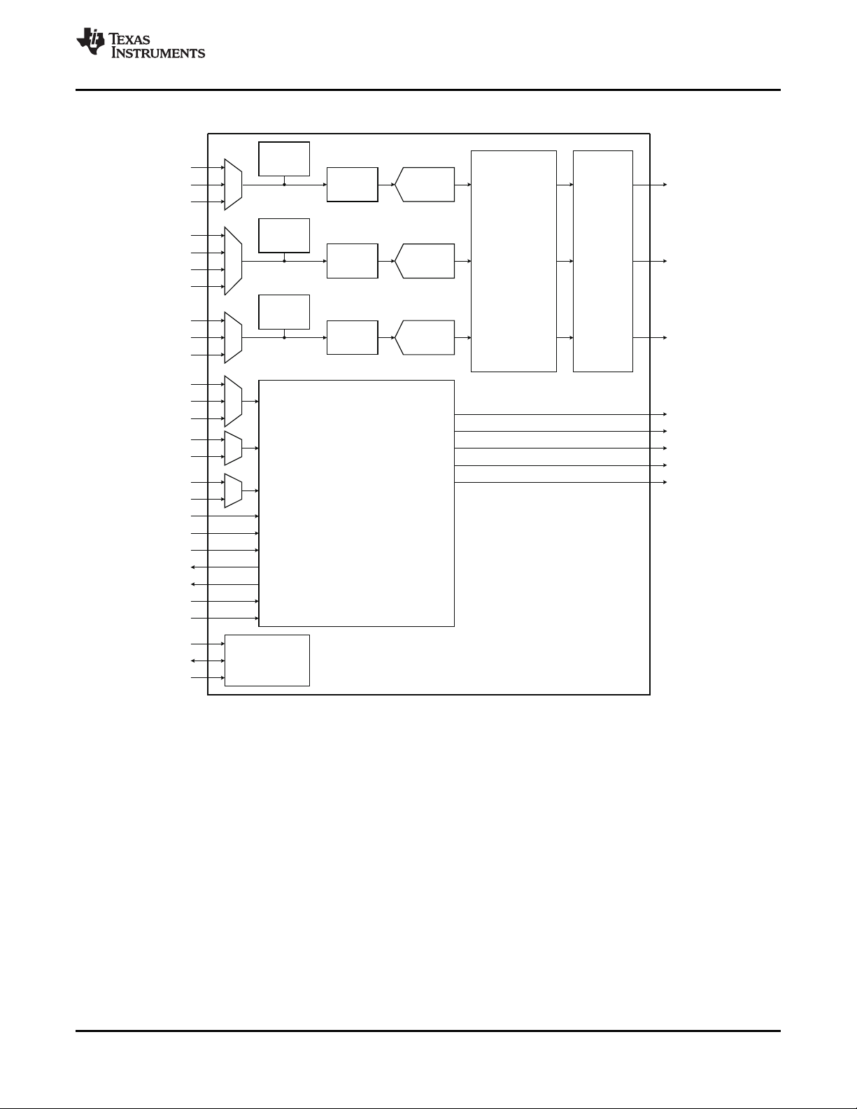
Output
Formatter
R[9:0]
G[9:0]
Host
Interface
Timing Processor
and
Clock Generation
RIN_1
SCL
SDA
I2CA
GIN_1
BIN_1
Clamp
Clamp
Clamp
Gain and
Offset
10-bit
ADC
HSYNC_A
VSYN C_A
COAST
CLAMP
FILT1
SOGIN_1
RESETB
PWDN
B[9:0]
SOGOUT
HSOUT
VSOUT
DATACLK
RIN_2
GIN_2
BIN_2
EXT_CLK
SOGIN_2
HSYNC_B
VSYN C_B
FILT2
RIN_3
GIN_3
GIN_4
SOGIN_3
BIN_3
FIDOUT
Color Space
Conversion
and
4:4:4 to 4:2:2
Conversion
Gain and
Offset
Gain and
Offset
10-bit
ADC
10-bit
ADC
TVP70025I
www.ti.com
...................................................................................................................................................................................................... SLES232 – JUNE 2008
FUNCTIONAL BLOCK DIAGRAM
Copyright © 2008, Texas Instruments Incorporated Submit Documentation Feedback 3
Product Folder Link(s): TVP70025I
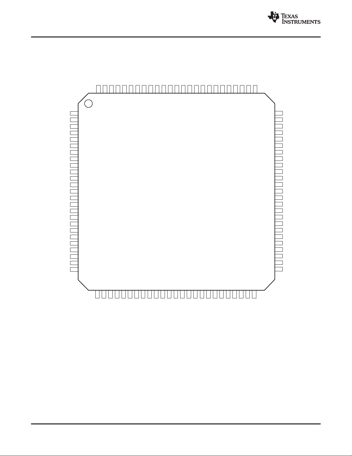
100-Pin TQFP Package
(TopView)
1 00
GIN_299SOGIN_2
98
GIN_397SOGIN_3
96
GIN_495A33GND
9
4
A33VDD
93
A33VDD
92
A33GND
91
NSUB90PLL_AGND89PLL_F88FIL
T2
87
FIL
T1
86
PLL_AGND85PLL_AVDD84PLL_AVDD83PLL_AGND82HSYNC_B
81
HSYNC_A
80
EXT_CLK
79
VSYNC_B
78
VSYNC_A
77
COAST76CLAMP
26
IOVDD
27
IOGND
28
ATACLK
29
B_9
30
B_8
31
B_7
32
B_6
33
B_5
34
B_4
35
B_3
36
B_2
37
B_1
38
B_0
39
DVDD
40
GND
41
IOVDD
42
IOGND
43
G_9
44
G_8
45
G_7
46
G_6
47
G_5
48
G_4
49
G_3
50
G_2
75
SDA
74
SCL
73
I2CA
72
TMS
71
RESETB
70
PWDN
69
DVDD
68
GND
67
IOGND
66
IOVDD
65
R_0
64
R_1
63
R_2
62
R_3
61
R_4
60
IOGND
59
R_5
58
R_6
57
R_7
56
R_8
55
R_9
54
IOGND
53
IOVDD
52
G_0
51
G_1
1
SOGIN_1
2
GIN_1
3
AGND
4
AVDD
5
A DGN
6
AVDD
7
AVDD
8
AGND
9
RI _N 3
10
RIN_2
11
RIN_1
12
A33GND
13
A33VDD
14
A33VDD
15
A33GND
16
BIN_3
17
BIN_2
18
BIN_1
19
AV DD
20
AGND
21
NSUB
22
FIDOUT
23
VSOUT
24
HSOUT
25
SOGOUT
TVP70025I
SLES232 – JUNE 2008 ......................................................................................................................................................................................................
www.ti.com
TERMINAL ASSIGNMENTS
4 Submit Documentation Feedback Copyright © 2008, Texas Instruments Incorporated
Product Folder Link(s): TVP70025I
TVP70025I
www.ti.com
...................................................................................................................................................................................................... SLES232 – JUNE 2008
TERMINAL FUNCTIONS
TERMINAL
NAME NO.
Analog Video
RIN_1 11 I Analog video input for R/Pr 1
RIN_2 10 I Analog video input for R/Pr 2
RIN_3 9 I Analog video input for R/Pr 3
GIN_1 2 I Analog video input for G/Y 1
GIN_2 100 I Analog video input for G/Y 2
GIN_3 98 I Analog video input for G/Y 3
GIN_4 96 I Analog video input for G/Y 4
BIN_1 18 I Analog video input for B/Pb 1
BIN_2 17 I Analog video input for B/Pb 2
BIN_3 16 I Analog video input for B/Pb 3
Clock Signals
DATACLK 28 O Data clock output
EXT_CLK 80 I External clock input. May be used as a timing reference for the mode detection block instead of
Digital Video
R[9:0] 55 – 59, 61 – 65 O Digital video output of R/Cr, R[9] is the most significant bit (MSB).
G[9:0] 43-52 O Digital video output of G/Y, G[9] is the MSB.
B[9:0] 29-38 O Digital video output of B/Cb, B[9] is the MSB.
Miscellaneous Signals
PWDN 70 I Power down input
RESETB 71 I Reset input, active low. Outputs are placed in a high-impedance mode during reset (see
TMS 72 I Test mode select input, active high. Used to enable scan test mode. For normal operation,
FILT1 87 O External filter connection for the horizontal PLL. A 0.1- µ F capacitor in series with a 1.5-k Ω
FILT2 88 O External filter connection for the horizontal PLL. A 4.7-nF capacitor should be connected from
PLL_F 89 I Horizontal PLL filter internal supply connection
Host Interface
I2CA 73 I I2C slave address input. Has internal pulldown resistor (see Table 6 ).
SCL 74 I I2C clock input
SDA 75 I/O I2C data bus
I/O DESCRIPTION
The inputs must be ac coupled. The recommended coupling capacitor is 0.1 µ F. Unused analog
inputs should be connected to ground using a 10-nF capacitor.
the internal clock reference. Also may be used as the ADC sample clock instead of the H-PLL
generated clock.
For 4:2:2 mode, multiplexed CbCr data is output on B[9:0].
Unused outputs can be left unconnected.
0 = Normal mode
1 = Power down
Table 7 ).
connect to ground.
resistor should be connected from this pin to pin 89 (see Figure 4 ).
this pin to pin 89 (see Figure 4 ).
0 = Slave address = B8h
1 = Slave address = BAh
Copyright © 2008, Texas Instruments Incorporated Submit Documentation Feedback 5
Product Folder Link(s): TVP70025I
TVP70025I
SLES232 – JUNE 2008 ......................................................................................................................................................................................................
TERMINAL FUNCTIONS (continued)
TERMINAL
NAME NO.
Power Supplies
NSUB 21, 91 I Substrate ground. Connect to analog ground.
A33VDD 13, 14, 93, 94 I Analog power. Connect to 3.3 V.
A33GND 12, 15, 92, 95 I Analog 3.3-V return. Connect to ground.
AGND 3, 5, 8, 20 I Analog 1.8-V return. Connect to ground.
AVDD 4, 6, 7, 19 I Analog power. Connect to 1.8 V.
PLL_AVDD 84, 85 I PLL analog power. Connect to 1.8 V.
PLL_AGND 83, 86, 90 I PLL analog power return. Connect to ground.
DGND 40, 68 I Digital return. Connect to ground.
DVDD 39, 69 I Digital power. Connect to 1.8 V.
IOGND 27, 42, 54, 60, I Digital power return. Connect to ground.
67
IOVDD 26, 41, 53, 66 I Digital power. Connect to 3.3 V or less for reduced noise.
Sync Signals
CLAMP 76 I External clamp input. Unused inputs can be connected to ground.
COAST 77 I External PLL COAST signal input. Unused inputs can be connected to ground.
VSYNC_A 78 I Vertical sync input A
VSYNC_B 79 I Vertical sync input B
HSYNC_A 81 I Horizontal sync input A
HSYNC_B 82 I Horizontal sync input B
SOGIN_1 1 I Sync-on-green input 1
SOGIN_2 99 I Sync-on-green input 2
SOGIN_3 97 I Sync-on-green input 3
FIDOUT 22 O Field ID output. Using register 17h, this pin also may be programmed to be the internal sync
VSOUT 23 O Vertical sync output
HSOUT 24 O Horizontal sync output
SOGOUT 25 O Sync-on-green slicer output
I/O DESCRIPTION
Unused inputs can be connected to ground.
Unused inputs can be connected to ground.
Unused inputs should be connected to ground using a 1-nF capacitor.
processing REFCLK output, coast output, clamp pulse output, or data enable.
www.ti.com
6 Submit Documentation Feedback Copyright © 2008, Texas Instruments Incorporated
Product Folder Link(s): TVP70025I
TVP70025I
www.ti.com
ABSOLUTE MAXIMUM RATINGS
...................................................................................................................................................................................................... SLES232 – JUNE 2008
(1)
over operating free-air temperature range (unless otherwise noted)
IOVDD to IOGND – 0.5 V to 4.5 V
Supply voltage range
DVDD to DGND – 0.5 V to 2.3 V
PLL_AVDD to PLL_AGND and AVDD to AGND – 0.5 V to 2.3 V
A33VDD to A33GND – 0.5 V to 4.5 V
Digital input voltage range VIto DGND – 0.5 V to 4.5 V
Analog input voltage range AIto A33GND – 0.2 V to 2.3 V
Digital output voltage range VOto DGND – 0.5 V to 4.5 V
T
A
T
stg
Operating free-air temperature range -40C to 85 ° C
Storage temperature range – 65 ° C to 150 ° C
(1) Stresses beyond those listed under Absolute Maximum Ratings may cause permanent damage to the device. These are stress ratings
only and functional operation of the device at these or any other conditions beyond those indicated under Recommended Operating
Conditions is not implied. Exposure to absolute-maximum-rated conditions for extended periods may affect device reliability.
RECOMMENDED OPERATING CONDITIONS
MIN NOM MAX UNIT
IOVDD Digital I/O supply voltage 3 3.3 3.6 V
DVDD Digital supply voltage 1.7 1.8 1.95 V
PLL_AVDD Analog supply voltage for horizontal PLL 1.7 1.8 1.95 V
AVDD Analog supply voltage 1.7 1.8 1.95 V
A33VDD Analog supply voltage 3 3.3 3.6 V
V
I(PP)
V
IH
V
IL
I
OH
I
OL
I
OH_DATACLK
I
OL_DATACLK
T
A
Analog input voltage (ac coupling necessary) 0.5 2 V
Digital input voltage high 0.7 IOVDD V
Digital input voltage low 0.3 IOVDD V
High-level output current 2 mA
Low-level output current – 2 mA
DATACLK high-level output current 4 mA
DATACLK low-level output current – 4 mA
ADC conversion rate 9 90 MHz
Operating free-air temperature – 40 85 ° C
Copyright © 2008, Texas Instruments Incorporated Submit Documentation Feedback 7
Product Folder Link(s): TVP70025I
TVP70025I
SLES232 – JUNE 2008 ......................................................................................................................................................................................................
ELECTRICAL CHARACTERISTICS
IOVDD = 3.3 V, DVDD = 1.8 V, PLL_AVDD = 1.8 V, AVDD = 1.8 V, A33VDD = 3.3 V, TA= 25 ° C
PARAMETER TEST CONDITIONS TYP
Power Supply
I
A33VDD
I
IOVDD
I
AVDD
I
PLL_VDD
I
DVDD
P
TOT
I
A33VDD
I
IOVDD
I
AVDD
I
PLL_VDD
I
DVDD
P
TOT
P
DOWN
(1) SMPTE color bar RGB input pattern used.
(2) Multi-burst input pattern used.
3.3-V supply current 480p (27 MSPS) 43 43 mA
3.3-V supply current 480p (27 MSPS) 11 14 mA
1.8-V supply current 480p (27 MSPS) 168 170 mA
1.8-V supply current 480p (27 MSPS) 11 11 mA
1.8-V supply current 480p (27 MSPS) 10 12 mA
Total power dissipation, normal mode 480p (27 MSPS) 518 535 mW
3.3-V supply current WXGA (85.5MSPS) 70 70 mA
3.3-V supply current WXGA (85.5 MSPS) 35 60 mA
1.8-V supply current WXGA (85.5 MSPS) 195 200 mA
1.8-V supply current WXGA (85.5 MSPS) 20 20 mA
1.8-V supply current WXGA (85.5 MSPS) 30 40 mA
Total power dissipation, normal mode WXGA (85.5 MSPS) 787 897 mW
Total power dissipation, power-down mode 15 15 mW
www.ti.com
(1)
(2)
TYP
UNIT
8 Submit Documentation Feedback Copyright © 2008, Texas Instruments Incorporated
Product Folder Link(s): TVP70025I
TVP70025I
www.ti.com
...................................................................................................................................................................................................... SLES232 – JUNE 2008
ELECTRICAL CHARACTERISTICS
IOVDD = 3.3 V, DVDD = 1.8 V, PLL_AVDD = 1.8 V, AVDD = 1.8 V, A33VDD = 3.3 V, TA= – 40 ° C to 85 ° C (unless otherwise
noted)
PARAMETER TEST CONDITIONS MIN TYP MAX UNIT
Analog Interface
Input voltage range By design 0.5 1 2 V
Z
I
Digital Logic Interface
C
I
Z
I
V
OH
V
OL
V
OH_SCLK
V
OL_SCLK
V
IH
V
IL
A/D CONVERTERS
DNL DC differential nonlinearity 10 bit, 90 MHz – 1 ± 0.5 +1 LSB
INL DC integral nonlinearity 10 bit, 90 MHz – 4 ± 1 +4 LSB
SNR Signal-to-noise ratio 10 MHz, 1 V
Horizontal PLL
Analog ADC Channel
Sync Processing
Input impedance, analog video inputs By design 500 k Ω
Input capacitance By design 10 pF
Input impedance By design 500 k Ω
Output voltage high IOH= 2 mA 0.8 IOVDD V
Output voltage low IOL= – 2 mA 0.2 IOVDD V
DATACLK output voltage high IOH= 4 mA 0.8 IOVDD V
DATACLK output voltage low IOH= – 2 mA 0.2 IOVDD V
High-level input voltage By design 0.7 IOVDD V
Low-level input voltage By design 0.3 IOVDD V
ADC full-scale input range Clamp disabled 0.95 1 1.05 V
ADC resolution 10-bit range 10 bits
Missing code 10 bit, 90 MHz none
at 90 MSPS 55 dB
PP
Analog 3-dB bandwidth 350 500 MHz
By design (W/O LPF) BW select
[3:0] = 0h
Phase adjustment 11.6 degree
VCO frequency range 9 90 MHz
Coarse gain full-scale control range Gain control value NG= 15 ± 6 dB
Coarse offset full-scale control range Referred to 10-bit ADC output ± 124 counts
Coarse offset step size Referred to 10-bit ADC output 4 counts
Internal clock reference frequency 5 6.5 7 MHz
pp
pp
Copyright © 2008, Texas Instruments Incorporated Submit Documentation Feedback 9
Product Folder Link(s): TVP70025I
DATACLK
t1
t2
t3
Valid Data
R, G, B, HSOUT
Valid Data
V
OH
V
OL
CLK POL = 0
CLK POL = 1
TVP70025I
SLES232 – JUNE 2008 ......................................................................................................................................................................................................
www.ti.com
TIMING REQUIREMENTS
PARAMETER TEST CONDITIONS
Clocks, Video Data, Sync Timing
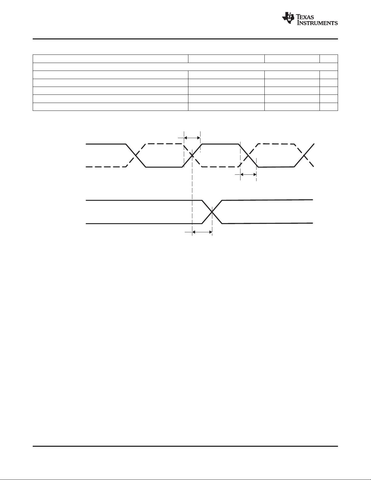
Positive Duty cycle DATACLK (CLK POL = 0) 48 50 52 %
Positive Duty cycle DATACLK (CLK POL = 1) 41 44 45 %
t1 DATACLK rise time 10% to 90% 1.2 ns
t2 DATACLK fall time 90% to 10% 1.2 ns
t3 R,G,B, HSOUT Output delay time 0 2 ns
(1) Measured at 90 MHz with 22- Ω series termination resistor and 10-pF load. Specified by characterization only. Data is clocked out on the
rising edge of DATACLK with Reg 18h CLK POL=0 and is clocked out on the falling edge of DATACLK with CLK POL=1.
(1)
MIN TYP MAX UNIT
Figure 1. Clock, Video Data, and HSOUT Timing
10 Submit Documentation Feedback Copyright © 2008, Texas Instruments Incorporated
Product Folder Link(s): TVP70025I
SDA
t1
t6
t7
t2
t8
t3
t4
t6
SCL
Data
Stop Start Stop
t5
TVP70025I
www.ti.com
...................................................................................................................................................................................................... SLES232 – JUNE 2008
TIMING REQUIREMENTS
PARAMETER TEST CONDITIONS MIN TYP MAX UNIT
I2C Host Port
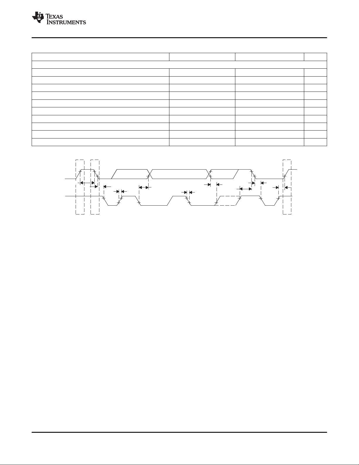
t1 Bus free time between Stop and Start Specified by design 1.3 µ s
t2 Setup time for a (repeated) Start condition Specified by design 0.6 µ s
t3 Hold time (repeated) Start condition Specified by design 0.6 µ s
t4 Setup time for a Stop condition Specified by design 0.6 ns
t5 Data setup time Specified by design 100 ns
t6 Data hold time Specified by design 0 0.9 µ s
t7 Rise time, SDA and SCL signal Specified by design 250 ns
t8 Fall time, SDA and SCL signal Specified by design 250 ns
C
b
f
I2C
Capacitive load for each bus line Specified by design 400 pF
I2C clock frequency Specified by design 400 kHz
Figure 2. I2C Host Port Timing
Copyright © 2008, Texas Instruments Incorporated Submit Documentation Feedback 11
Product Folder Link(s): TVP70025I
TVP70025I
SLES232 – JUNE 2008 ......................................................................................................................................................................................................
www.ti.com
FUNCTIONAL DESCRIPTION
Analog Channel
The TVP70025I contains three identical analog channels that are independently programmable. Each channel
consists of a clamping circuit, programmable gain control, programmable offset control, and an A/D converter.
Analog Input Switch Control
TVP70025I has three analog channels that accept up to ten video inputs. The user can configure the internal
analog video switches via the I2C interface. The ten analog video inputs can be used for different input
configurations, some of which are:
• Up to three SDTV, EDTV, or HDTV component video inputs (limited by number of SOG inputs)
• Up to two 5-wire PC graphics inputs (limited by number of HSYNC and VSYNC inputs)
The input selection is performed by the input select register at I2C subaddress 19h a 1Ah (see Input
Mux Select 1 and Input Mux Select 2).
Supported Video Formats
The TVP70025I supports A/D conversion of SDTV (480i, 576i), EDTV (480p, 576p), and HDTV (720p, 1080i)
YPbPr component video inputs. The TVP70025I also supports A/D conversion and color space conversion of all
standard PC graphics formats (RGB) from VGA up to WXGA 60Hz.
A summary of the analog video standards supported by the TVP70025I module is shown in the Table below.
Analog Video Standards
VIDEO FORMAT VIDEO STANDARDS
SDTV (YPbPr Component) 480i, 576i
EDTV (YPbPr Component) 480p, 576p
HDTV (YPbPr Component) 720p, 1080i
PC graphics (RGB Component) VGA - XGA 75Hz, WXGA
SCART (RGB Component) 576i
Analog Input Clamping
The TVP70025I provides dc restoration for all analog video inputs including the SOG slicer inputs. The dc
restoration circuit (a.k.a. clamp circuit) restores the ac-coupled video signal to a fixed dc level. One dc restoration
circuit is implemented prior to each of the three A/D converters, and a fourth one is located prior to the SOG
slicer. The dc restoration circuit can be programmed to operate as either a sync-tip clamp (a.k.a. coarse clamp)
or a back-porch clamp (a.k.a. fine clamp). The sync-tip clamp always clamps the video sync-tip level near the
bottom of the A/D converter range. The back-porch type clamp supports two clamping levels (bottom level and
mid level) that are selectable using bits 0, 1, and 2 of register 10h. When using the fine bottom-level clamp, an
optional 300-mV common-mode offset may be selected using bit 7 of register 2Ah.
In general, the analog video input being used for horizontal synchronization purposes should always use the
sync-tip clamp; all other analog video inputs should use the back-porch clamp. The advantage of the back-porch
clamp is that it has negligible video droop or tilt across a video line.
12 Submit Documentation Feedback Copyright © 2008, Texas Instruments Incorporated
Product Folder Link(s): TVP70025I
TVP70025I
www.ti.com
...................................................................................................................................................................................................... SLES232 – JUNE 2008
The selection between bottom- and mid-level clamping is performed by I2C subaddress 10h (see Section
Sync-On-Green Threshold). The fine clamps also must be enabled via I2C register 2Ah for proper operation. The
internal clamping time can be adjusted using the I2C clamp start and width registers at subaddress 05h and 06h,
respectively (see Clamp Start and Clamp Width).
Table 1. Recommended Clamp Setting by Video Mode
VIDEO MODE
YPbPr Component Coarse Fine Bottom Level Fine Mid Level Fine Mid Level
PC Graphics Coarse Fine Bottom Level Fine Bottom Level Fine Bottom Level
SCART-RGB Coarse Fine Bottom Level Fine Bottom Level Fine Bottom Level
SOG INPUT GREEN ADC CHANNEL RED ADC CHANNEL BLUE ADC CHANNEL
(Y/G) (Y/G) (Pr/R) (Pb/B)
A single-pole low-pass filter with three selectable cutoff frequencies (0.5, 1.7, and 4.8 MHz) is implemented in the
feedback loop of the sync-tip clamp circuit.
Programmable Gain Control
The TVP70025I provides a 4-bit coarse analog gain control (before A/D conversion) and an 8-bit fine digital gain
control (after A/D conversion). The coarse analog gain and the fine digital gain are both independently
programmable for each ADC channel.
Coarse Gain Control
The 4-bit coarse analog gain control has a 4:1 linear gain control range defined by the following equation.
Coarse Gain = 0.5 + N
/10, where 0 ≤ N
CG
≤ 15
CG
0.5 ≤ Coarse Gain ≤ 2.0
Default: N
The 4-bit coarse gain control can scale a signal with a voltage-input compliance of 0.5 V
10-bit A/D output code range. The minimum gain corresponds to a code 0h (2-V
while the maximum gain corresponds to code Fh (0.5-V
= 7 (Coarse Gain = 1.2)
CG
to 2 V
PP
full-scale input, – 6-dB gain)
full scale, +6-dB gain). The 4-bit coarse gain control is
PP
PP
to a full-scale
PP
independently controllable for each ADC channel (Red Coarse Gain, Green Coarse Gain, and Blue Coarse
Gain).
Fine Gain Control
The 8-bit fine digital gain control has a 2:1 linear gain control range defined by the following equation.
Fine Gain = 1.0 + N
/256 where 0 ≤ N
FG
≤ 255
FG
1.0 ≤ Fine Gain < 2.0
Default: N
= 0 (Fine Gain = 1.0)
FG
The 8-bit fine gain control is independently controllable for each ADC channel (Red Fine Gain, Green Fine Gain,
and Blue Fine Gain). For a normal PC graphics input, the fine gain is used mostly.
Programmable Offset Control
The TVP70025I provides a 6-bit coarse analog offset control (before A/D conversion) and a 10-bit fine digital
offset control (after A/D conversion). The coarse analog offset and the fine digital offset are both independently
programmable for each ADC channel.
Coarse Offset Control
A 6-bit code sets the coarse offset (Red Coarse Offset, Green Coarse Offset, Blue Coarse Offset) with individual
adjustment per channel. The coarse offset ranges from – 32 counts to +31 counts. The coarse offset registers
apply before the ADC.
Fine Offset Control
A 10-bit fine offset registers (Red Fine Offset, Green Fine Offset, Blue Fine Offset) apply after the ADC. The fine
offset ranges from – 512 counts to +511 counts.
Copyright © 2008, Texas Instruments Incorporated Submit Documentation Feedback 13
Product Folder Link(s): TVP70025I
COAST
HSYNC
Phase
Detector
PLL Control
Register 03h
Bit [5:3]
PLL Control
Register 03h
Bit [7:6]
Phase Select
Register 04h
Bit [7:3]
Charge
Pump
VCO
Phase
Select
Divider
ADC
Sampling
CLK
External
Clock
PLL Divide
Register 01h and 02h
1:0]Bit [1
Loop
Filter
N = 1 or 2
Post
Divider
÷N
Post Divider
Register 04h
Bit [0]
TVP70025I
SLES232 – JUNE 2008 ......................................................................................................................................................................................................
www.ti.com
Automatic Level Control (ALC)
The ALC circuit maintains the level of the signal to be set at a value that is programmed at the fine offset I2C
register. It consists of a pixel averaging filter and feedback loop. This ALC function can be enabled or disabled by
the I2C register at subaddress 26h.
The ALC circuit needs a timing pulse generated internally but the user should program the position properly. The
ALC pulse must be positioned after the clamp pulse. The position of ALC pulse is controlled by ALC placement
I2C register at address 31h. This is available only for internal ALC pulse timing. When using an external clamp
pulse, the fine clamp and the ALC both start on the leading edge of the external clamp pulse. Therefore, it is
recommended to keep the external clamp pulse as long as possible.
Analog-to-Digital Converters (ADCs)
All ADCs have a resolution of 10 bits and can operate up to 90 MSPS. All A/D channels receive an identical
clock from the on-chip phase-locked loop (PLL) at a frequency between 12 MHz and 90 MHz. All ADC reference
voltages are generated internally. The external sampling clock also can be used.
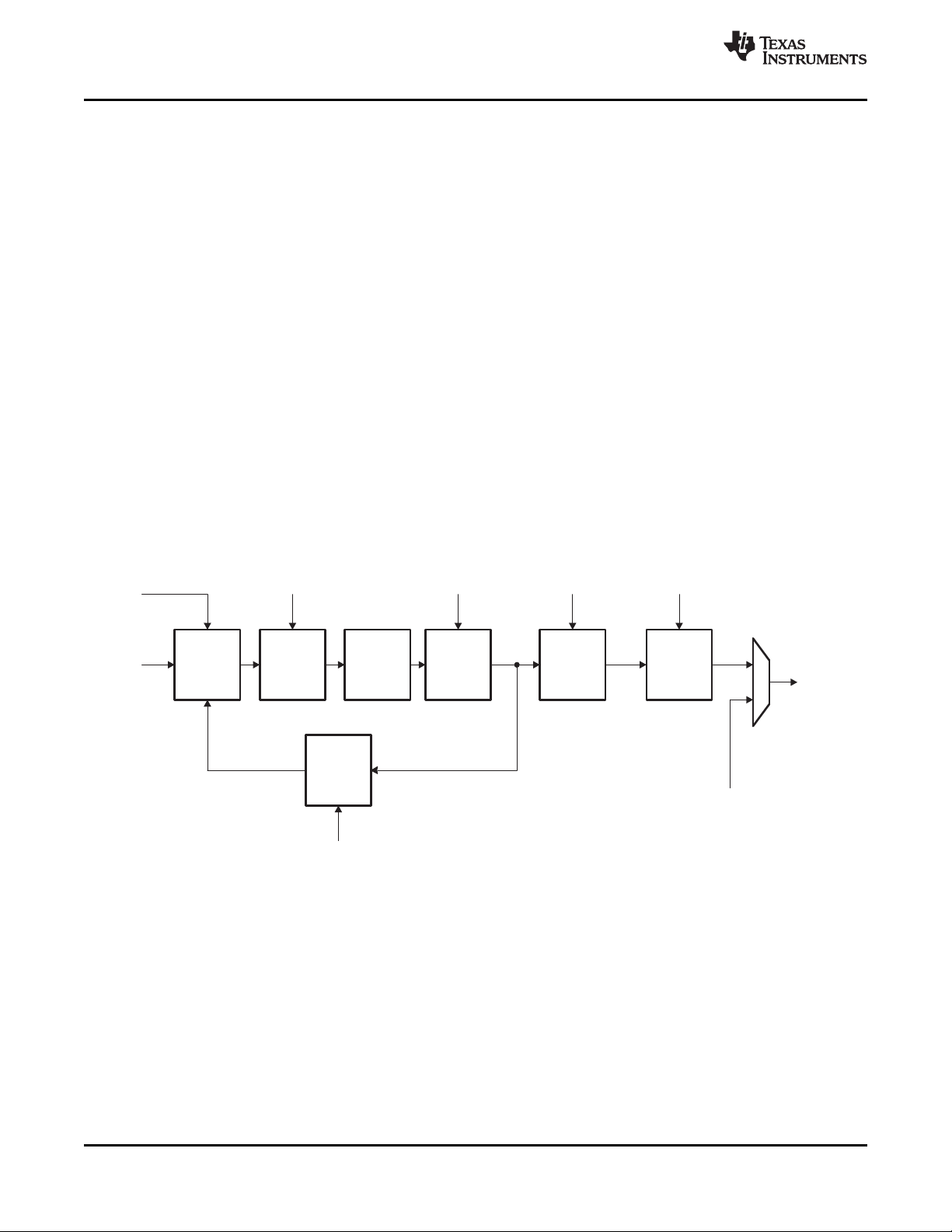
Horizontal PLL
The horizontal PLL generates a high-frequency internal clock used by the ADC sampling and data clocking out to
derive the pixel output frequency with programmable phase. The reference signal for this PLL is the horizontal
sync signal supplied on the HSYNC input or from extracted horizontal sync of the sync slicer block for embedded
sync signals. The horizontal PLL consists of a phase detector, charge pump, loop filter, voltage controlled
oscillator (VCO), phase select, feedback divider, and post divider. The horizontal PLL block diagram is shown in
Figure 3 .
Figure 3. Horizontal PLL Block Diagram
The COAST signal is used to allow the H-PLL to keep running at the same frequency, in the absence of the
incoming HSYNC signal or disordered HSYNC period. This is useful during the vertical sync period, or any other
time that the HSYNC is not available. The fine clamp is disabled during the H-PLL coast interval.
There are several PLL controls to produce the correct sampling clock. The 12-bit feedback divider register is
programmable to select exact multiplication number to generate the pixel clock in the range of 12 MHz to
90 MHz. The 3-bit loop filter current control register is to control the charge pump current that drives the low-pass
loop filter. The applicable current values are listed in Table 2 .
14 Submit Documentation Feedback Copyright © 2008, Texas Instruments Incorporated
Product Folder Link(s): TVP70025I
0.1 µF
4.7 nF
1.5 kW
TVP70025I
PLL_F
FILT2
FILT1
89
88
87
TVP70025I
www.ti.com
...................................................................................................................................................................................................... SLES232 – JUNE 2008
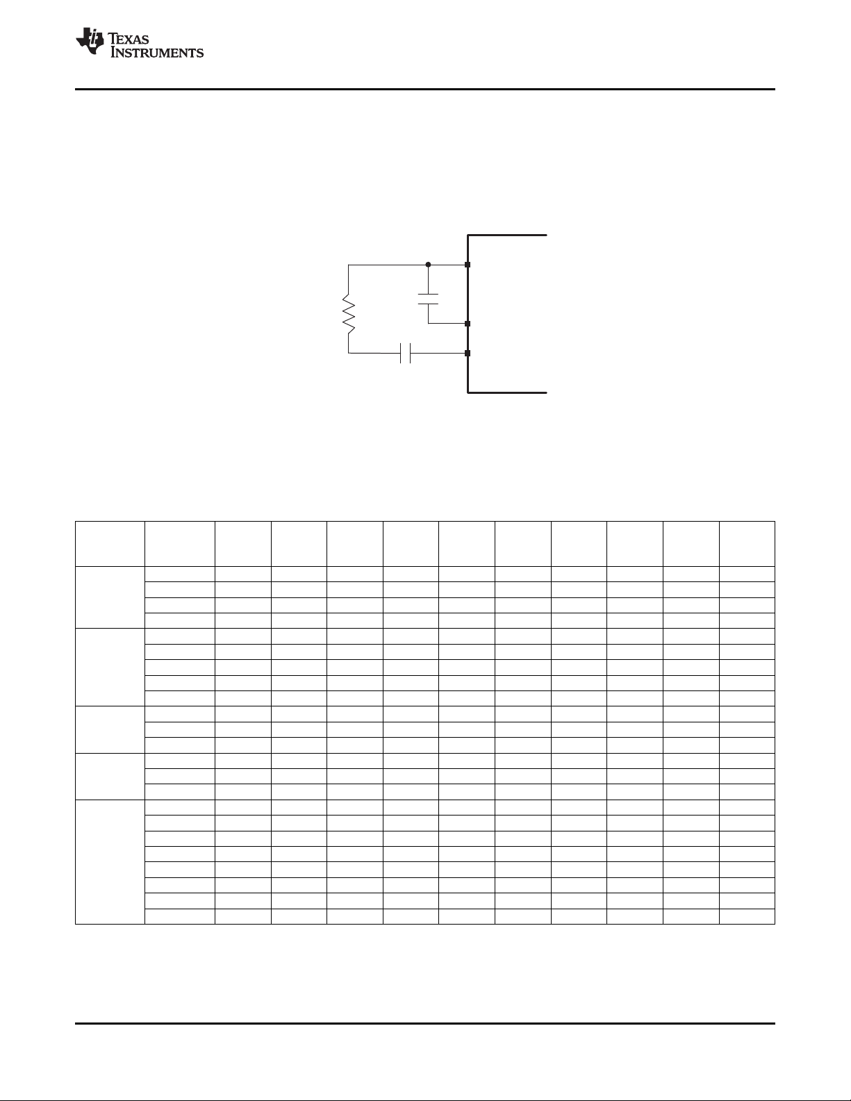
The purpose of the 2-bit VCO range control is to improve the noise performance of the TVP70025I. The
frequency ranges for the VCO are shown in Table 2 . The phase of the ADC sample clock generated by the
horizontal PLL can be accurately controlled in 32 uniform steps over a single clock period
(360/32 = 11.25 degrees phase resolution) using the phase select register located at subaddress 04h.
The horizontal PLL characteristics are determined by the loop filter design, the PLL charge pump current, and the
VCO range setting. The loop filter design is shown in Figure 4 . Supported settings of VCO range and charge
pump current for VESA standard display modes are listed in Table 2 .
Figure 4. Horizontal PLL Loop Filter
In addition to sourcing the ADC sample clock from the horizontal PLL, an external pixel clock can be used (from
pin 80).
Table 2. Recommended VCO Range and Charge Pump Current Settings
for Supporting Standard Display Formats
STANDARD RESOLUTION RATE RATE [11:4] REG [3:0] REG REG 03h DIVIDER
640 × 480 59.94 31.469 25.175 800 32h 00h 20h 0 ULow (00b) 100b
VGA
SVGA 800 × 600 72.188 48.077 50 1040 41h 00h 58h 0 Low (01b) 011b
XGA 1024 × 768 70.069 56.476 75 1328 53h 00h A8h 0 Med (10b) 101b
WXGA 1280 × 768 59.87 47.776 79.5 1664 68h 00h A0h 0 Med (10b) 100b
Video
640 × 480 72.809 37.861 31.5 832 34h 00h 20h 0 ULow (00b) 100b
640 × 480 75 37.5 31.5 840 34h 80h 20h 0 ULow (00b) 100b
640 × 480 85.008 43.269 36 832 34h 00h 60h 0 Low (01b) 100b
800 × 600 56.25 35.156 36 1024 40h 00h 58h 0 Low (01b) 011b
800 × 600 60.317 37.879 40 1056 42h 00h 58h 0 Low (01b) 011b
800 × 600 75 46.875 49.5 1056 42h 00h 58h 0 Low (01b) 011b
800 × 600 85.061 53.674 56.25 1048 41h 80h 58h 0 Low (01b) 011b
1024 × 768 60.004 48.363 65 1344 54h 00h 58h 0 Low (01b) 011b
1024 × 768 75.029 60.023 78.75 1312 52h 00h A8h 0 Med (10b) 101b
1280 × 768 59.995 47.396 68.25 1440 5Ah 00h 50h 0 Low (01b) 010b
1440 x 900 59.01 55.469 88.75 1600 64h 00h A0h 0 Med (10b) 100b
720 × 480i 29.97 15.374 13.5 858 35h A0h 18h 0 ULow (00b) 011b
720 × 576i 25 15.625 13.5 864 36h 00h 18h 0 ULow (00b) 011b
720 × 480p 59.94 31.469 27 858 35h A0h 18h 0 ULow (00b) 011b
720 × 576p 50 31.25 27 864 36h 00h 18h 0 ULow (00b) 011b
1280 × 720p 60 45 74.25 1650 67h 20h A0h 0 Med (10b) 100b
1280 × 720p 50 37.5 74.25 1980 7Bh C0h 98h 0 Med (10b) 011b
1920 × 1080i 60 33.75 74.25 2200 89h 80h 98h 0 Med (10b) 011b
1920 × 1080i 50 28.125 74.25 2640 A5h 00h 90h 0 Med (10b) 010b
FRAME PIXEL PLLDIV PLLDIV OUTPUT
(Hz) (MHz) 01h [7:0] 02h [7:4] REG 04h [0]
LINE RATE DIVIDER RANGE CURRENT
(kHz) TOTAL REG 03h REG 03h
PLL VCO CP
PIX/LINE [7:6] [5:3]
Product Folder Link(s): TVP70025I
Copyright © 2008, Texas Instruments Incorporated Submit Documentation Feedback 15

TVP70025I
SLES232 – JUNE 2008 ......................................................................................................................................................................................................
www.ti.com
RGB-to-YCbCr Color Space Conversion
The TVP70025I supports RGB-to-YCbCr color space conversion (CSC) with I2C programmable coefficients. The
TVP70025I should default to the CSC coefficients required for HDTV component video inputs. The TVP70025I
supports the ability to bypass the CSC block and defaults to the bypass mode (bit 3of subaddress 23h).
RGB-to-YCbCr CSC coefficients for HDTV component video (see CEA-770.3-C, ITU-R BT.709)
(default coefficients):
G ' B ' R '
Y 00000016E3 000000024F 00000006CE
Pb FFFFFFF3AB 0000001000 FFFFFFFC55
Pr FFFFFFF178 FFFFFFFE88 0000001000
RGB-to-YCbCr CSC coefficients for SDTV component video (see CEA-770.2-C, ITU-R BT.601)
(informative only):
G ' B ' R '
Y 00000012C9 00000003A6 0000000991
Pb FFFFFFF566 0000001000 FFFFFFFA9A
Pr FFFFFFF29A FFFFFFFD66 0000001000
4:4:4 to 4:2:2 Conversion
For 4:4:4 YPbPr component video inputs, the TVP70025I can downsample the chroma samples (CbCr) from 1 ×
to 0.5 × using a 27-tap half-band filter.
NOTE:
• Selection between the 30-bit 4:4:4 output format and the 20-bit 4:2:2 output format is made
using bit 1 of register 15h.
• Multiplexed CbCr data is output on BOUT [9:0] in the 20-bit 4:2:2 output format.
• 4:4:4 to 4:2:2 conversion is implemented after RGB-to-YCbCr color space conversion.
16 Submit Documentation Feedback Copyright © 2008, Texas Instruments Incorporated
Product Folder Link(s): TVP70025I

TVP70025I
www.ti.com
...................................................................................................................................................................................................... SLES232 – JUNE 2008
Sync Processing
Horizontal Sync Selection
The TVP70025I provides two HSYNC inputs and three analog SOG inputs for HDTV and PC graphics inputs.
The sync input used by the horizontal PLL is automatically selected based on activity detection.
Sync Slicer
TVP70025I includes a circuit that compares the input signal on Green channel to a level 150 mV (typical value)
above the clamped level (sync tip). The slicing level is programmable by I2C register subaddress at 10h. The
digital output of the composite sync slicer is available on the SOGOUT pin.
Noise Immunity
In general, noise on a slowly varying input signal (i.e., sync falling edge) may cause a voltage comparator to
false trigger as the input passes through the linear range of the comparator. To improve the overall performance
of the TVP70025I sync slicer in the presence of noise on the SOG input, the voltage comparator includes
hysteresis. Maintaining a 50% slice level using the I2C programmable slice level control can further improve the
noise immunity of the Sync slicer. The slice level is programmable in 11.2-mV increments over a 350-mV range
as follows.
slice_level = (350 mV) × (N
where 0 ≤ N
≤ 31, default: 11
TH
0 ≤ slice_level ≤ 350 mV
Glitch Immunity
During white-to-black transitions, the input video waveform may undershoot below the sync slicer threshold. To
help attenuate the amplitude of such glitches, a single-pole low-pass filter with three selectable cutoff frequencies
(2.5, 10, and 33 MHz) is provided at the input of the SOG voltage comparator circuit. This filter is bypassed in the
default mode.
/31)
TH
NOTE:
Although the low-pass filter may attenuate the amplitude of glitches present on the
SOG input, it also makes the sync falling edge less sharp.
Sync Separator
The sync separator automatically extracts VSYNC and HSYNC from the sliced composite sync input supplied at
the SOG input. The G or Y input containing the composite sync must be ac coupled to the SOG input pin using a
1-nF capacitor. Support for PC graphics, SDTV, EDTV, and HDTV up to 1080i is provided.
Sync Activity Detection
The TVP70025I provides activity detection on the sync inputs (VSYNC, HSYNC) to enable the host processor to
determine whether the PC graphics source is configured as a 3-wire, 4-wire, or 5-wire interface as defined here:
• 5 wire (G, B, R, HSYNC, VSYNC)
• 4 wire (G, B, R, CSYNC)
• 3 wire (G, B, R with SOG)
If activity is detected on the VSYNC input, the host processor should assume that the PC graphics input is a
standard 5-wire interface. In this case, the HSYNC input of the TVP70025I should be configured as an HSYNC
input. If AHSO and AVSO are set for automatic selection in I2C Reg 0Eh, the TVP70025I automatically uses the
HSYNC and VSYNC inputs, provided signals are present at both inputs.
Copyright © 2008, Texas Instruments Incorporated Submit Documentation Feedback 17
Product Folder Link(s): TVP70025I

TVP70025I
SLES232 – JUNE 2008 ......................................................................................................................................................................................................
www.ti.com
If activity is detected on the HSYNC input but not on the VSYNC input, the host processor should assume that
the PC graphics input is a standard 4-wire interface. In this case, the HSYNC input of the TVP70025I should be
used as a digital CSYNC input. If AHSO and AVSO are set for automatic selection, VSYNC is properly decoded
from the CSYNC input, provided no signal is present at the VSYNC input pin. Some test sources output CSYNC
on both the HSYNC pin and the VSYNC pin. In this case, the active VSYNC source (AVSS) must be manually
set to Sync separated VSYNC in Reg 0Eh. The TVP70025I supports the following two types of CSYNC inputs.
CSYNC = VSYNC XOR HSYNC (default)
CSYNC = VSYNC OR HSYNC
If activity is not detected on either the HSYNC input or the VSYNC input, the host processor should assume that
the PC graphics input is a standard 3-wire interface. With AHSO and AVSO set for automatic selection and no
signals present at the HSYNC and VSYNC input pins, the TVP70025I automatically selects the SOG input as the
sync source.
VSYNC INPUT HSYNC INPUT PC GRAPHICS
ACTIVITY DETECT ACTIVITY DETECT INPUT TYPE
1 1 5 wire (default)
1 0 Undefined (assume 5 wire)
0 1 4 wire
0 0 3 wire
The activity detection status for the VSYNC and HSYNC inputs is written to the I2C status register at subaddress
14h.
NOTE:
Pin 13 of a standard 15-pin VGA video connector can be either a horizontal sync
(HSYNC) or a composite sync (CSYNC).
NOTE:
For component video inputs, the active HSYNC and VSYNC should always be derived
from the selected SOG input. This can most easily be ensured by setting the AHSO,
AVSO, AHSS and AVSS bit fields in register 0Eh to logic 1.
NOTE:
For proper operation when separate HSYNC and VSYNC inputs are used, the leading
edge of VSYNC must not be precisely aligned with the leading edge of HSYNC. A
simple RC delay circuit provides adequate delay in most applications.
18 Submit Documentation Feedback Copyright © 2008, Texas Instruments Incorporated
Product Folder Link(s): TVP70025I

0
1
VSYNC
Activity
Detect
AVSS(Reg0E[0])
0
1
SOG (sliced)
AHSS(Reg0E[3])
0
1
VSINV(Reg36[3])
0
1
HSYNC
0
1
AHSO(Reg0E[4])
AVSO(Reg0E[1])
Sync Processor
(Sync Separator,
Sync Accumulator)
PLL
0 1
0
1
VS_Select(Reg22[0])
0 1
0
1
Sync Timing
HSYNC
Ext_COAST
DATA CLK
SOG OUT
VSYNC
VSYNC Alignment
VSOP(Reg0E[2])
VS OUT
HSBP(Reg36[0])
HSYNC bypass
HS OUT
0
1
COAST_sel(Reg0F[5])
COASTHSYNC
AVS(Reg14[3])
AHS(Reg14[6])
VSBP(Reg36[1])
Activity
Detect
Activity
Detect
TVP70025I
www.ti.com
...................................................................................................................................................................................................... SLES232 – JUNE 2008
Figure 5. Sync Processing
Copyright © 2008, Texas Instruments Incorporated Submit Documentation Feedback 19
Product Folder Link(s): TVP70025I

TVP70025I
SLES232 – JUNE 2008 ......................................................................................................................................................................................................
Output Formatter
The output formatter sets how the data is formatted for output on the TVP70025I output buses. Table 3 shows
the available component video output modes.
Table 3. YCbCr Component Video Output Formats
TERMINAL NAME TERMINAL NUMBER 30-BIT 4:2:2 YCbCr 20-BIT 4:2:2 YCbCr
G_9 43 Y9 Y9
G_8 44 Y8 Y8
G_7 45 Y7 Y7
G_6 46 Y6 Y6
G_5 47 Y5 Y5
G_4 48 Y4 Y4
G_3 49 Y3 Y3
G_2 50 Y2 Y2
G_1 51 Y1 Y1
G_0 52 Y0 Y0
B_9 29 Cb9 Cb9, Cr9
B_8 30 Cb8 Cb8, Cr8
B_7 31 Cb7 Cb7, Cr7
B_6 32 Cb6 Cb6, Cr6
B_5 33 Cb5 Cb5, Cr5
B_4 34 Cb4 Cb4, Cr4
B_3 35 Cb3 Cb3, Cr3
B_2 36 Cb2 Cb2, Cr2
B_1 37 Cb1 Cb1, Cr1
B_0 38 Cb0 Cb0, Cr0
R_9 29 Cr9
R_8 30 Cr8
R_7 31 Cr7
R_6 32 Cr6
R_5 33 Cr5
R_4 34 Cr4
R_3 35 Cr3
R_2 36 Cr2
R_1 37 Cr1
R_0 38 Cr0
(1) 10-bit 4:2:2 YCbCr output format (i.e., ITU-R BT.656) is not supported by the TVP70025I.
< br/ >
NOTE:
In the 20-bit 4:2:2 YCbCr output mode, the unused Red outputs (Cr[9:0]) are placed in
a high-impedance state.
(1)
www.ti.com
20 Submit Documentation Feedback Copyright © 2008, Texas Instruments Incorporated
Product Folder Link(s): TVP70025I

TVP70025I
www.ti.com
...................................................................................................................................................................................................... SLES232 – JUNE 2008
Embedded Syncs
Standard embedded syncs insert SAV and EAV codes into the data stream on the rising and falling edges of
AVID. These codes contain the V and F bits that also define vertical timing. Table 4 gives the format of the SAV
and EAV codes.
H = 1 always indicates EAV. H = 0 always indicates SAV. The alignment of V and F to the line and field counter
varies depending on the standard. The P bits are protection bits:
P3 = V xor H
P2 = F xor H
P1 = F xor V
P0 = F xor V xor H
Table 4. EAV and SAV Sequence
Y9 (MSB) Y8 Y7 Y6 Y5 Y4 Y3 Y2 Y1 Y0
Preamble 1 1 1 1 1 1 1 1 1 1
Preamble 0 0 0 0 0 0 0 0 0 0
Preamble 0 0 0 0 0 0 0 0 0 0
Status 1 F V H P3 P2 P1 P0 0 0
The insertion location of the SAV/EAV codes on a video line is programmable using the AVID start/stop pixel
values located at subaddresses 40h through 43h.
NOTE:
When enabled (bit 0 of subaddress 15h), embedded syncs are present in both the Y
and C outputs.
Output Range Limits
The TVP70025I provides selectable output range limits in I2C subaddress 15h:
00 = RGB coding range (Y, Cb, and Cr range from 0 to 1023) (default)
01 = Extended coding range (Y, Cb, and Cr range from 4 to 1019)
10 = ITU-R BT.601 coding range (Y ranges from 64 to 940, Cb and Cr range from 64 to 960)
11 = Reserved
NOTE:
RGB coding range not allowed with embedded syncs.
Power Management
The TVP70025I supports both automatic and manual power-down modes. The automatic power-down mode can
be selected by setting bit 2 of subaddress 0Fh to logic 0.
In the automatic power-down mode, the TVP70025I powers down the ADCs, the ADC reference, and horizontal
PLL when activity is not detected on both the selected HSYNC input and the selected SOG input (VSYNC is no
longer used). The TVP70025I restores power whenever activity is detected on either the selected HSYNC input
or the selected SOG input.
The TVP70025I also can be placed in power-down mode via the active-high PWDN input (pin 70). When the
PWDN input is driven high, the TVP70025I powers down everything including the I2C interface, and the digital
outputs are not placed in a high-impedance mode.
The TVP70025I also can be placed in a power-down mode using bit 1 of register 0Fh.
Individual blocks of the TVP70025I can be independently powered down using register 2Bh.
Copyright © 2008, Texas Instruments Incorporated Submit Documentation Feedback 21
Product Folder Link(s): TVP70025I
RGBin
HSYNC
DATACLK
RGBout
D0 D1 D3 D4 D5
P0 P1 P3
...
P10 P11
P12
HSOUT
Programmable Width
NPDclockslatency
HSOUT Programmable Start
4:4:4 RGB/YCbCr Output Timing. Npd = 18 clock cycles. HSOUT start is programmable in register 21h.
RGBin
HSYNC
DATACLK
Gout
Y0 Y1 Y3 Y4 Y5
P0 P1 P3
...
P10 P11
P12
HSOUT
Programmable Width
NPDclocks latency
U0 V1 U2 V3 U4
Bout
HSOUT Programmable Start
4:2:2 YCbCr Output Timing. Npd = 39 clock cycles. HSOUT start is programmable in register 21h.
TVP70025I
SLES232 – JUNE 2008 ......................................................................................................................................................................................................
www.ti.com
Timing
The TVP70025I supports RGB/YCbCr 4:4:4 and YCbCr 4:2:2 modes. Output timing is shown in Figure 6 . All
timing diagrams are shown for operation with internal PLL clock at phase 0 and HSOUT Output Start = 0. For the
4:2:2 mode, CbCr data output is on the BOUT[9:0] output port.
22 Submit Documentation Feedback Copyright © 2008, Texas Instruments Incorporated
Figure 6. Output Timing Diagram
Product Folder Link(s): TVP70025I

TVP70025I
www.ti.com
...................................................................................................................................................................................................... SLES232 – JUNE 2008
I2C Host Interface
Communication with the TVP70025I device is via an I2C host interface. The I2C standard consists of two signals,
serial input/output data (SDA) line and input clock line (SCL), which carry information between the devices
connected to the bus. A third signal (I2CA) is used for slave address selection. Although an I2C system can be
multi-mastered, the TVP70025I can function as a slave device only.
Since SDA and SCL are kept open drain at logic high output level or when the bus is not driven, the user should
connect SDA and SCL to a positive supply voltage via a pullup resistor on the board. SDA is implemented
bidirectional. The slave addresses select, terminal 73 (I2CA), enables the use of two TVP70025I devices tied to
the same I2C bus, as it controls the least significant bit of the I2C device address
Table 5. I2C Host Interface Terminal Description
SIGNAL TYPE DESCRIPTION
I2CA I Slave address selection
SCL I Input clock line
SDA I/O Input/output data line
Reset and I2C Bus Address Selection
The TVP70025I can respond to two possible chip addresses. The address selection is made at reset by an
externally supplied level on the I2CA pin. The TVP70025I device samples the level of terminal 73 at power up or
at the trailing edge of RESETB and configures the I2C bus address bit A0. The I2CA terminal has an internal
pulldown resistor to pull the terminal low to set a zero.
Table 6. I2C Host Interface Device Addresses
A6 A5 A4 A3 A2 A1 A0 (I2C A) R/W HEX
1 0 1 1 1 0 0 (default) 1/0 B9h/B8h
1 0 1 1 1 0 1
(1) If terminal 73 is strapped to IOVDD via a 2.2-k Ω resistor, I2C device address A0 is set to 1.
(1)
1/0 BBh/BAh
I2C Operation
Data transfers occur utilizing the following illustrated formats.
S 10111000 ACK Subaddress ACK Send data ACK P
Read from I2C control registers
S 10111000 ACK Subaddress ACK S 10111001 ACK Receive data NAK P
S = I2C bus Start condition
P = I2C bus Stop condition
ACK = Acknowledge generated by the slave
NAK = Acknowledge generated by the master, for multiple byte read master with ACK each byte except last byte
Subaddress = Subaddress byte
Data = Data byte, if more than one byte of DATA is transmitted (read and write), the subaddress pointer is
automatically incremented
I2C bus address = Example shown that I2CA is in default mode; Write (B8h), Read (B9h).
Copyright © 2008, Texas Instruments Incorporated Submit Documentation Feedback 23
Product Folder Link(s): TVP70025I

Power
Reset
I C
2
5 ms
1 µs
TVP70025I
SLES232 – JUNE 2008 ......................................................................................................................................................................................................
www.ti.com
Power Up, Reset, and Initialization
No specific power-up sequence is required, but all power supplies should be active and stable within 500 ms of
each other. RESETB may be low during power up, but must remain low for at least 1 µ s after the power supplies
become stable. Alternatively, reset may be asserted any time with minimum 5-ms delay after power-up and must
remain asserted for at least 1 µ s. Reset timing is shown in Figure 7 . I2C SCL and SDA signals must not change
state until the TVP70025I reset sequence has been completed. Keeping RESETB low prior to any I2C activity
prevents this. Table 7 shows the status of the TVP70025I terminals during and immediately after reset.
Table 7. Output Mode Per Reset Sequence State
SIGNAL NAME
R[9:0], B[9:0], G[9:0] High-impedance
HSOUT, VSOUT, FIDOUT, DATACLK High-impedance
SOGOUT High- ↑ impedance
DURING RESET RESET COMPLETED
OUTPUT MODE
Default condition
(see bit 0 of subaddress 17h)
Default condition
(see bit 0 of subaddress 17h)
Default condition
(see bit 1 of subaddress 17h)
Figure 7. Reset Timing
24 Submit Documentation Feedback Copyright © 2008, Texas Instruments Incorporated
Product Folder Link(s): TVP70025I
TVP70025I
www.ti.com
...................................................................................................................................................................................................... SLES232 – JUNE 2008
CONTROL REGISTERS
The TVP70025I is initialized and controlled by a set of internal registers that define the operating parameters of
the entire device. Communication between the external controller and the TVP70025I is through a standard I2C
host port interface, as previously described.
Table 8 shows the summary of these registers. Detailed programming information for each register is described
in the following sections.
Table 8. Control Registers Summary
REGISTER NAME I2C SUBADDRESS DEFAULT R/W
Chip Revision 00h 02h R
H-PLL Feedback Divider MSBs 01h 67h R/W
H-PLL Feedback Divider LSBs 02h 20h R/W
H-PLL Control 03h A8h R/W
H-PLL Phase Select 04h 80h R/W
Clamp Start 05h 32h R/W
Clamp Width 06h 20h R/W
HSYNC Output Width 07h 20h R/W
Blue Fine Gain 08h 00h R/W
Green Fine Gain 09h 00h R/W
Red Fine Gain 0Ah 00h R/W
Blue Fine Offset MSBs 0Bh 80h R/W
Green Fine Offset MSBs 0Ch 80h R/W
Red Fine Offset MSBs 0Dh 80h R/W
Sync Control 1 0Eh 5Bh R/W
H-PLL and Clamp Control 0Fh 2Eh R/W
Sync On Green Threshold 10h 5Dh R/W
Sync Separator Threshold 11h 20h R/W
H-PLL Pre-Coast 12h 00h R/W
H-PLL Post-Coast 13h 00h R/W
Sync Detect Status 14h R
Output Formatter 15h 04h R/W
MISC Control 1 16h 11h R/W
MISC Control 2 17h 03h R/W
MISC Control 3 18h 00h R/W
Input Mux Select 1 19h 00h R/W
Input Mux Select 2 1Ah C2h R/W
Blue and Green Coarse Gain 1Bh 77h R/W
Red Coarse Gain 1Ch 07h R/W
Fine Offset LSBs 1Dh 00h R/W
Blue Coarse Offset 1Eh 10h R/W
Green Coarse Offset 1Fh 10h R/W
Red Coarse Offset 20h 10h R/W
HSOUT Output Start 21h 0Dh R/W
MISC Control 4 22h 08h R/W
Blue Digital ALC Output LSBs 23h R
Green Digital ALC Output LSBs 24h R
(1) (2)
(3)
(1) For proper operation of the TVP70025I device, the default settings for all register locations designated as " Reserved " in the register map
summary should never be changed from the values provided.
(2) For registers with reserved bits, a 0b must be written to reserved bit locations, unless otherwise stated.
(3) R = Read only, W = Write only, R/W = Read/Write
Copyright © 2008, Texas Instruments Incorporated Submit Documentation Feedback 25
Product Folder Link(s): TVP70025I

TVP70025I
SLES232 – JUNE 2008 ......................................................................................................................................................................................................
Table 8. Control Registers Summary (continued)
REGISTER NAME I2C SUBADDRESS DEFAULT R/W
Red Digital ALC Output LSBs 25h R
Automatic Level Control Enable 26h 80h R/W
Digital ALC Output MSBs 27h R
Automatic Level Control Filter 28h 53h R/W
Reserved 29h 08h R/W
Fine Clamp Control 2Ah 07h R/W
Power Control 2Bh 00h R/W
ADC Setup 2Ch 50h R/W
Coarse Clamp Control 2Dh 00h R/W
SOG Clamp 2Eh 80h R/W
RGB Coarse Clamp Control 2Fh 8Ch R/W
SOG Coarse Clamp Control 30h 04h R/W
ALC Placement 31h 5Ah R/W
Reserved 32h 18h R/W
Reserved 33h 60h R/W
Macrovision Stripper Width 34h 03h R/W
VSYNC Alignment 35h 10h R/W
Sync Bypass 36h 00h R/W
Lines Per Frame Status 37h – 38h R
Clocks Per Line Status 39h – 3Ah R
HSYNC Width 3Bh R
VSYNC Width 3Ch R
Line Length Tolerance 3Dh 03h R/W
Reserved 3Eh 04h R/W
Video Bandwidth Control 3Fh 00h R/W
AVID Start Pixel 40h – 41h 012Ch R/W
AVID Stop Pixel 42h – 43h 062Ch R/W
VBLK Field 0 Start Line Offset 44h 05h R/W
VBLK Field 1 Start Line Offset 45h 05h R/W
VBLK Field 0 Duration 46h 1Eh R/W
VBLK Field 1 Duration 47h 1Eh R/W
F-bit Field 0 Start Line Offset 48h 00h R/W
F-bit Field 1 Start Line Offset 49h 00h R/W
1st CSC Coefficient 4Ah – 4Bh 16E3h R/W
2nd CSC Coefficient 4Ch – 4Dh 024Fh R/W
3rd CSC Coefficient 4Eh – 4Fh 06CEh R/W
4th CSC Coefficient 50h – 51h F3ABh R/W
5th CSC Coefficient 52h – 53h 1000h R/W
6th CSC Coefficient 54h – 55h FC55h R/W
7th CSC Coefficient 56h – 57h F178h R/W
8th CSC Coefficient 58h – 59h FE88h R/W
9th CSC Coefficient 5Ah – 5Bh 1000h R/W
Reserved 5Ch – 5Dh 0000h R/W
Reserved 5Eh – FFh 0000h R/W
www.ti.com
(3)
26 Submit Documentation Feedback Copyright © 2008, Texas Instruments Incorporated
Product Folder Link(s): TVP70025I
TVP70025I
www.ti.com
...................................................................................................................................................................................................... SLES232 – JUNE 2008
Register Definitions
Chip Revision
Subaddress 00h Read Only
7 6 5 4 3 2 1 0
Chip revision [7:0]
Chip revision [7:0]: Chip revision number. The chip revision number is 02h for the TVP70025I.
NOTE:
The TVP70025I has a chip revision number that is unique from the TVP7000 and
TVP7001 devices.
H-PLL Feedback Divider MSBs
Subaddress 01h Default (67h)
7 6 5 4 3 2 1 0
PLL divide [11:4]
PLL divide [11:0]: Controls the 12-bit horizontal PLL feedback divider value that determines the number of pixels per line. PLL divide [11:4]
bits should be loaded first whenever a change is required.
H-PLL Feedback Divider LSBs
Subaddress 02h Default (20h)
7 6 5 4 3 2 1 0
PLL divide [3:0] Reserved
PLL divide [11:0]: Controls the 12-bit horizontal PLL feedback divider value that determines the number of pixels per line. PLL divide [11:4]
bits should be loaded first whenever a change is required.
H-PLL Control
Subaddress 03h Default (A8h)
7 6 5 4 3 2 1 0
VCO [1:0] Charge Pump Current [2:0] Reserved
VCO [1:0]: Selects VCO gain (K
frequency range.
VCO Gain
(K
00 = 75 Ultra low PCLK < 36 MHz
01 = 85 Low 36 MHz ≤ PCLK < 70 MHz
10 = 150 Medium (default) 70 MHz ≤ PCLK ≤ 90 MHz
11 = Reserved Reserved Reserved
Charge Pump Current [2:0]: Selects PLL charge pump current setting. The recommended charge pump current setting (ICP) can be
determined using the following equation.
000 = 0: Small
101 = 5 (default)
111 = 7: Large
NOTE: Also see the PLL and CLAMP Control register at subaddress 0Fh.
VCO
ICP= 40 × K
VCO
)
VCO
) and corresponding output
VCO Range Pixel Clock Frequency (PCLK)
/(pixels per line)
Copyright © 2008, Texas Instruments Incorporated Submit Documentation Feedback 27
Product Folder Link(s): TVP70025I

TVP70025I
SLES232 – JUNE 2008 ......................................................................................................................................................................................................
www.ti.com
H-PLL Phase Select
Subaddress 04h Default (80h)
7 6 5 4 3 2 1 0
Phase Select [4:0] Reserved DIV2
Phase Select [4:0]: ADC sampling clock phase select. (1 LSB = 360/32 = 11.25 ° ). A host-based automatic phase control algorithm can be
used to control this setting to optimize graphics sampling phase.
00h = 0 degrees
10h = 180 degrees (default)
1Fh = 348.75 degrees
DIV2: DATACLK divide-by-2. H-PLL post divider. May be used with 2x H-PLL Feedback Divider to improve jitter performance, when lower
freqeuncy SDTV formats are used.
0 = DATACLK/1 (default)
1 = DATACLK/2
Clamp Start
Subaddress 05h Default (32h)
7 6 5 4 3 2 1 0
Clamp Start [7:0]
Clamp Start [7:0]: Positions the clamp signal an integer number of clock periods after the HSYNC signal. If external clamping is selected this
value has no meaning. See Table 9 for the recommended settings.
Clamp Width
Subaddress 06h Default (20h)
7 6 5 4 3 2 1 0
Clamp Width [7:0]
Clamp Width [7:0]: Sets the width in pixels for the fine clamp. See also register Clamp Start (subaddress 05h).
Table 9. Recommended Fine Clamp Settings
VIDEO STANDARD CLAMP START CLAMP WIDTH
HDTV (tri-level) 50 (32h) 32 (20h)
SDTV (bi-level) 6 (06h) 16 (10h)
PC graphics 6 (06h) 16 (10h)
HSYNC Output Width
Subaddress 07h Default (20h)
7 6 5 4 3 2 1 0
HSOUT Width [7:0]
HSOUT Width [7:0]: Sets the width in pixels for HSYNC output.
Blue Fine Gain
Subaddress 08h Default (00h)
7 6 5 4 3 2 1 0
Blue Fine Gain [7:0]
Blue Fine Gain [7:0]: 8-bit fine digital gain (contrast) for Blue channel (applied after the ADC). Offset binary value.
Blue Fine Gain = 1 + Blue Fine Gain [7:0]/256
Blue Fine Gain [7:0] Blue Fine Gain
00h 1.0 (default)
80h 1.5
FFh 2.0
28 Submit Documentation Feedback Copyright © 2008, Texas Instruments Incorporated
Product Folder Link(s): TVP70025I

TVP70025I
www.ti.com
...................................................................................................................................................................................................... SLES232 – JUNE 2008
Green Fine Gain
Subaddress 09h Default (00h)
7 6 5 4 3 2 1 0
Green Fine Gain [7:0]
Green Fine Gain [7:0]: 8-bit fine digital gain (contrast) for Green channel (applied after the ADC). Offset binary value.
Green Fine Gain = 1 + Green Fine Gain [7:0]/256
Green Fine Gain [7:0] Green Fine Gain
00h 1.0 (default)
80h 1.5
FFh 2.0
Red Fine Gain
Subaddress 0Ah Default (00h)
7 6 5 4 3 2 1 0
Red Fine Gain [7:0]
Red Fine Gain [7:0]: 8-bit fine digital gain (contrast) for Red channel (applied after the ADC). Offset binary value.
Red Fine Gain = 1 + Red Fine Gain [7:0]/256
Red Fine Gain [7:0] Red Fine Gain
00h 1.0 (default)
80h 1.5
FFh 2.0
Blue Fine Offset MSBs
Subaddress 0Bh Default (80h)
7 6 5 4 3 2 1 0
Blue Fine Offset [9:2]
Blue Fine Offset [9:2]: Eight MSBs of 10-bit fine digital offset (brightness) for Blue channel (applied after ADC). Corresponding two LSBs
located at register 1Dh. Offset binary value.
The default setting of 80h places the bottom-level (RGB) clamped output blank levels at 0 and mid-level clamped (PbPr) output blank levels
at 512.
FFh = Maximum blue fine offset MSBs
81h = 1 count (out of 256)
80h = 0 (default)
7Fh = – 1 count (out of 256)
00h = Minimum blue fine offset MSBs
Green Fine Offset MSBs
Subaddress 0Ch Default (80h)
7 6 5 4 3 2 1 0
Green Fine Offset [9:2]
Green Fine Offset [9:2]: Eight MSBs of 10-bit fine digital offset (brightness) for Green channel (applied after ADC). Corresponding two LSBs
located at register 1Dh. Offset binary value.
The default setting of 80h places the bottom-level (RGB) clamped output blank levels at 0 and mid-level clamped (PbPr) output blank levels
at 512.
FFh = Maximum green fine offset MSBs
81h = 1 count (out of 256)
80h = 0 (default)
7Fh = – 1 count (out of 256)
00h = Minimum green fine offset MSBs
Copyright © 2008, Texas Instruments Incorporated Submit Documentation Feedback 29
Product Folder Link(s): TVP70025I

TVP70025I
SLES232 – JUNE 2008 ......................................................................................................................................................................................................
www.ti.com
Red Fine Offset MSBs
Subaddress 0Dh Default (80h)
7 6 5 4 3 2 1 0
Red Fine Offset [9:2]
Red Fine Offset [9:2]: 8 MSBs of 10-bit fine digital offset (brightness) for Red channel (applied after ADC). Corresponding two LSBs located
at register 1Dh. Offset binary value.
The default setting of 80h places the bottom-level (RGB) clamped output blank levels at 0 and mid-level clamped (PbPr) output blank levels
at 512.
FFh = Maximum red fine offset MSBs
81h = 1 count (out of 256)
80h = 0 (default)
7Fh = – 1 count (out of 256)
00h = Minimum red fine offset MSBs
Sync Control 1
Subaddress 0Eh Default (5Bh)
7 6 5 4 3 2 1 0
HSPO HSIP HSOP AHSO AHSS VSOP AVSO AVSS
HSPO: HSYNC polarity override
0 = Polarity determined by chip (default)
1 = Polarity set by bit 6 in register 0Eh (not recommended)
HSIP: HSYNC input polarity
0 = Indicates input HSYNC polarity active low
1 = Indicates input HSYNC polarity active high (default)
HSOP: HSYNC output polarity
0 = Active-low HSYNC output (default)
1 = Active-high HSYNC output
NOTE: HSOP has no effect in raw sync bypass mode. See register 36h.
AHSO: Active HSYNC override
0 = Active HSYNC is automatically selected by TVP70025I. If selected, SOG and HSYNC inputs both have active inputs,
HSYNC is selected as the active sync source. The selected active HSYNC is provided via the AHS status bit (bit 6 of
register 14h).
1 = Active HSYNC is manually selected via the AHSS control bit (bit 3 of register 0Eh). (default)
AHSS: Active HSYNC select. The indicated HSYNC is used only if the AHSO control bit (bit 4) is set to 1 or if activity is detected on both the
selected HSYNC input and the selected SOG input (bits 1, 7 = 1 in register 14h).
0 = Active HSYNC is derived from the selected HSYNC input.
1 = Active HSYNC is derived from the selected SOG input (default).
VSOP: VSYNC output polarity
0 = Active-low VSYNC output (default)
1 = Active-high VSYNC output
AVSO: Active VSYNC override
0 = Active VSYNC is automatically selected by TVP70025I. If selected, SOG and VSYNC inputs both have active inputs,
VSYNC is selected as the active sync source. The selected active VSYNC is provided via the AVS status bit (bit 3 of
register 14h).
1 = Active VSYNC is manually selected via the AVSS control bit (bit 0 of register 0Eh) (default).
NOTE: Automatic sync selection should be enabled only for 5-wire PC graphics inputs.
AVSS: Active VSYNC select. This bit is effective when the AVSO control bit (bit 1) is set to 1.
0 = Active VSYNC is derived from the selected VSYNC input.
1 = Active VSYNC is derived from the Sync separated VSYNC (default).
30 Submit Documentation Feedback Copyright © 2008, Texas Instruments Incorporated
Product Folder Link(s): TVP70025I
TVP70025I
www.ti.com
...................................................................................................................................................................................................... SLES232 – JUNE 2008
H-PLL and Clamp Control
Subaddress 0Fh Default (2Eh)
7 6 5 4 3 2 1 0
CF CP Coast Sel CPO CPC SMO FCPD ADC Test
CF: Clamp Function. Clamp pulse select. This control bit determines whether the timing for both the fine clamp and the ALC circuit are
generated internally or externally.
0 = Internal fine clamp and ALC timing (default)
1 = External fine clamp and ALC timing (pin 76)
CP: Clamp Polarity. External clamp polarity select
0 = Active-high clamp pulse (default)
1 = Active-low clamp pulse
CS: Coast Select. Coast signal select. This control bit determines whether the timing for H-PLL coast signal is generated internally or
externally.
0 = External H-PLL coast timing (pin 77)
1 = Internal H-PLL coast timing (default)
CPO: Coast Polarity Override
0 = Polarity determined by chip (default)
1 = Polarity set be Bit 3 in register 0Fh
CPC: Coast Polarity Change. External coast polarity select
0 = Active-low coast signal
1 = Active-high coast signal (default)
SMO: Seek Mode Override. Places the TVP70025I in a low power mode whenever no activity is detected on the selected sync inputs.
0 = Enable automatic power management mode
1 = Disable automatic power management mode (default)
NOTE: Digital outputs are not high impedance and may be in a random state during low power mode. Outputs can be put
in high impedance state by I2C register 17h.
FCPD: Full Chip Power Down. Active-low power down. FCPD powers down all blocks except I2C. The I2C register values are retained.
0 = Power-down mode
1 = Normal operation (default)
NOTE: Digital outputs are not high impedance and may be in random state during FCPD. Outputs can be put in high
impedance state by I2C register 17h.
ADC Test: Active-high ADC test mode select. When placed in the ADC test mode, the TVP70025I disables the fine clamp, enables the
coarse clamp, and selects the external clock input (pin 80) for each ADC channel.
0 = ADC test mode disabled (default)
1 = ADC test mode enabled
NOTE: Also see the Horizontal PLL Control register at subaddress 03h.
Sync-On-Green Threshold
Subaddress 10h Default (5Dh)
7 6 5 4 3 2 1 0
SOG Threshold [4:0] Blue CS Green CS Red CS
SOG Threshold [4:0]: Sets the voltage level of the SOG slicer comparator according to the following equation.
slice_level = (350 mV) × (N
00h = 0 mV
0Bh = 124 mV (default)
1Fh = 350 mV
Blue Clamp Select: This bit has no effect when the Blue channel fine clamp is disabled (bit 2 of subaddress 2Ah).
0 = Bottom-level fine clamp
1 = Mid-level fine clamp (default)
Green Clamp Select: This bit has no effect when the Green channel fine clamp is disabled (bit 1 of subaddress 2Ah).
0 = Bottom-level fine clamp (default)
1 = Mid level fine clamp
Red Clamp Select: This bit has no effect when the Red channel fine clamp is disabled (bit 0 of subaddress 2Ah).
0 = Bottom-level fine clamp
1 = Mid-level fine clamp (default)
NOTE: Bottom-level clamping is required for Y and RGB inputs, while mid-level clamping is required for Pb and Pr inputs. The internal clamp
pulse also must be correctly positioned for proper clamp operation (see register 05h)
Copyright © 2008, Texas Instruments Incorporated Submit Documentation Feedback 31
TH
/31)
Product Folder Link(s): TVP70025I

TVP70025I
SLES232 – JUNE 2008 ......................................................................................................................................................................................................
Sync Separator Threshold
Subaddress 11h Default (20h)
7 6 5 4 3 2 1 0
Sync Separator Threshold [7:0]
Sync Separator Threshold [7:0]: Sets how many internal clock reference periods the sync separator counts to before toggling high or low.
Sync Separator Threshold [7:0] × (minimum clock period) must be greater than the width of the negative sync pulse. This setting also can
affect the position of the VSOUT (see register 22h).
NOTE: The internal clock reference is typically 6.5 MHz, but a minimum clock period of 133 ns is recommended to allow for clock variation.
40h = Recommended setting for support of most standard formats.
H-PLL Pre-Coast
Subaddress 12h Default (00h)
7 6 5 4 3 2 1 0
Pre-Coast [7:0]
Pre-Coast [7:0]: Sets the number of HSYNC periods that coast becomes active prior to VSYNC leading edge. A minimum setting of 1 is
required to ensure generation of an internal coast signal.
00h = Minimum setting (default)
01h = 1 HSYNC period (recommendation)
FFh = Maximum setting
H-PLL Post-Coast
Subaddress 13h Default (00h)
www.ti.com
7 6 5 4 3 2 1 0
Post-Coast [7:0]
Post-Coast [7:0]: Sets the number of HSYNC periods that coast stays active following VSYNC trailing edge.
Table 10. Recommended H-PLL Pre-Coast and H-PLL Post-Coast Settings
STANDARD H-PLL PRE_COAST H-PLL POST-COAST
480i/p with Macrovision 3 03h
576i/p with Macrovision 3 03h
720p 1 0
1080i 1 0
PC Graphics with SOG 1 0
32 Submit Documentation Feedback Copyright © 2008, Texas Instruments Incorporated
Product Folder Link(s): TVP70025I

TVP70025I
www.ti.com
...................................................................................................................................................................................................... SLES232 – JUNE 2008
Sync Detect Status
Subaddress 14h Read Only
7 6 5 4 3 2 1 0
HSD AHS IHSPD VSD AVS VSPD SOGD ICPD
HSD: HSYNC Detect. HSYNC activity detection for selected HSYNC input (pin 81 or 82).
0 = No HSYNC activity detected
1 = HSYNC activity detected
AHS: Active HSYNC. Indicates whether the active HSYNC is derived from the selected HSYNC input or the selected SOG input.
0 = HSYNC from selected HSYNC input (pin 81 or 82)
1 = HSYNC from selected SOG input (pin 1, 99, or 97)
IHSPD: Input HSYNC Polarity Detect. HSYNC polarity detection for selected HSYNC input (pin 81 or 82).
0 = Active-low HSYNC
1 = Active-high HSYNC
VSD: VSYNC Detect. VSYNC activity detection for selected VSYNC input (pin 78 or 79).
0 = No VSYNC activity detected
1 = VSYNC activity detected
AVS: Active VSYNC. Indicates whether the active VSYNC is derived from the selected VSYNC input or the sync separator.
0 = VSYNC from selected VSYNC input (pin 78 or 79)
1 = VSYNC from sync separator
VSPD: Input VSYNC Polarity Detect. VSYNC polarity detection for selected VSYNC input (pin 78 or 79).
0 = Active-low VSYNC
1 = Active-high VSYNC
SOGD: SOG Detect. SOG activity detection for selected SOG input (pin 1, 99, or 97).
0 = No SOG activity detected
1 = SOG activity detected
ICPD: Input Coast Polarity Detect. Coast signal polarity detection.
0 = Active-low coast signal
1 = Active-high coast signal
NOTE:
See the Sync Control register at subaddress 0Eh.
Copyright © 2008, Texas Instruments Incorporated Submit Documentation Feedback 33
Product Folder Link(s): TVP70025I

TVP70025I
SLES232 – JUNE 2008 ......................................................................................................................................................................................................
Output Formatter
Subaddress 15h Default (04h)
7 6 5 4 3 2 1 0
Reserved Output code range [1:0] Reserved Clamp REF CbCr order 422/444 Sync En
Reserved [7]:
0 = Required (default)
Output code range [1:0]:
00 = RGB coding range (Y, Cb, and Cr range from 0 to 1023) (default)
01 = Extended coding range (Y, Cb, and Cr range from 4 to 1019)
10 = ITU-R BT.601 coding range (Y ranges from 64 to 940, Cb and Cr range from 64 to 960)
11 = Reserved
Reserved [4]:
0 = Required (default)
Clamp REF: Selects which edge of HSYNC is used as the timing reference for the fine clamp pulse placement and also the ALC placement.
0 = Clamp pulse placement referred to the trailing edge of HSYNC (default)
1 = Clamp pulse placement referred to the leading edge of HSYNC
CbCr order: This bit is only effective in the 4:2:2 output mode (i.e., bit 1 is set to 1).
0 = CbCr order
1 = CrCb order (default)
422/444: Active-high 4:4:4 to 4:2:2 decimation filter enable
0 = 30-bit 4:4:4 output format (default)
1 = 20-bit 4:2:2 output format
Notes:
1. Multiplexed CbCr data is output on BOUT [9:0] in the 20-bit 4:2:2 output format.
2. 10-bit 4:2:2 output format is not supported.
Sync En: Active-high embedded sync enable
0 = Embedded sync disabled (default)
1 = Embedded sync enabled
Notes:
1. Embedded syncs are not supported when the RGB coding range (0 to 1023) is selected.
2. Embedded syncs are not supported when the 30-bit 4:4:4 output format is selected.
3. Discrete syncs are always enabled except when outputs are placed in the high-impedance mode.
4. When enabled, embedded syncs are present in both the Y and C outputs.
www.ti.com
MISC Control 1
Subaddress 16h Default (11h)
7 6 5 4 3 2 1 0
Reserved CbCr Align Reserved PLL PD STRTB
CbCr Align: CbCr alignment
0 = Alternative operation
1 = Normal operation (default)
PLL PD: Active-high H-PLL power down
0 = Normal operation (default)
1 = H-PLL powered down
STRTB: Active-high H-PLL start-up circuit enable
0 = H-PLL start-up circuit disabled
1 = H-PLL start-up circuit enabled (default)
34 Submit Documentation Feedback Copyright © 2008, Texas Instruments Incorporated
Product Folder Link(s): TVP70025I

TVP70025I
www.ti.com
...................................................................................................................................................................................................... SLES232 – JUNE 2008
MISC Control 2
Subaddress 17h Default (03h)
7 6 5 4 3 2 1 0
Reserved Test output control [2:0] Reserved SOG En Output En
Test output control [2:0]: Selects which signal is output on pin 22. Output polarity control is also provided using bit 2 of subaddress 18h.
000 = Field ID output (default)
001 = Data Enable output
010 = Reserved
011 = Reserved
100 = Internal clock reference output (~6.5 MHz typical)
101 = Coast output
110 = Clamp pulse output
111 = High-impedance mode
SOG En: Active-low output enable for SOGOUT output.
0 = SOG output enabled
1 = SOG output placed in high-impedance mode (default)
Output En: Active-low output enable for RGB, DATACLK, HSOUT, VSOUT, and FIDOUT outputs. This control bit allows selecting a
high-impedance output mode for multiplexing the output of the TVP70025I with another device.
0 = Outputs enabled
1 = Outputs placed in high-impedance mode (default)
NOTE: Data Enable output is equivalent to the internal active video signal that is controlled by the AVID start/stop pixel
values and the VBLK offset/duration line values.
MISC Control 3
Subaddress 18h Default (00h)
7 6 5 4 3 2 1 0
Reserved Reserved Blank En CSC En Reserved FID POL SOG POL CLK POL
Reserved [7]:
0 = Required (default)
Blank En: Active-high blank level enable. Forces the video blank level to a standard value when using embedded syncs.
0 = Normal operation (default)
1 = Force standard blank levels
CSC En: Active-high CSC enable. When disabled, the CSC block is bypassed.
0 = CSC disabled (default)
1 = CSC enabled
FID POL: Active-high Field ID output polarity control. Under normal operation, the field ID output is set to logic 1 for an odd field (field 1) and
set to logic 0 for an even field (field 0).
0 = Normal operation (default)
1 = FID output polarity inverted
NOTE: This control bit also affects the polarity of the data enable output when selected (see Test output control [2:0] at
subaddress 17h).
SOG POL: Active-high SOG output polarity control
0 = Normal operation (default)
1 = SOG output polarity inverted
CLK POL: Allows selecting the polarity of the output data clock.
0 = Data is clocked out on rising edge of DATACLK (default)
1 = Data is clocked out on falling edge of DATACLK
Copyright © 2008, Texas Instruments Incorporated Submit Documentation Feedback 35
Product Folder Link(s): TVP70025I

TVP70025I
SLES232 – JUNE 2008 ......................................................................................................................................................................................................
Input Mux Select 1
Subaddress 19h Default (00h)
7 6 5 4 3 2 1 0
SOG Select [1:0] Red Select [1:0] Green Select [1:0] Blue Select [1:0]
SOG Select [1:0]: Selects one of three SOG inputs.
00 = SOGIN_1 input selected (default)
01 = SOGIN_2 input selected
10 = SOGIN_3 input selected
11 = Reserved
Red Select [1:0]: Selects one of three R/Pr inputs.
00 = RIN_1 input selected (default)
01 = RIN_2 input selected
10 = RIN_3 input selected
11 = Reserved
Green Select [1:0]: Selects one of four G/Y inputs.
00 = GIN_1 input selected (default)
01 = GIN_2 input selected
10 = GIN_3 input selected
11 = GIN_4 input selected
Blue Select [1:0]: Selects one of three B/Pb inputs.
00 = BIN_1 input selected (default)
01 = BIN_2 input selected
10 = BIN_3 input selected
11 = Reserved
www.ti.com
36 Submit Documentation Feedback Copyright © 2008, Texas Instruments Incorporated
Product Folder Link(s): TVP70025I

TVP70025I
www.ti.com
...................................................................................................................................................................................................... SLES232 – JUNE 2008
Input Mux Select 2
Subaddress 1Ah Default (C2h)
7 6 5 4 3 2 1 0
SOG LPF SEL [1:0] CLP LPF SEL [1:0] CLK SEL VS SEL PCLK SEL HS SEL
SOG LPF SEL [1:0]: SOG low-pass filter selection. The SOG low-pass filter is used to attenuate any glitches present on
the SOG input.
00 = 2.5-MHz low-pass filter
01 = 10-MHz low-pass filter
10 = 33-MHz low-pass filter
11 = Low-pass filter bypass (default)
NOTE: The SOG LPF setting can affect HSYNC delay in the TVP70025I. Additionally, excessive filtering of HDTV and
graphics SOG sources can lead to sync attenuation and sync extraction issues.
CLP LPF SEL [1:0]: Coarse clamp low-pass filter selection. This filter affects the operation of all enabled coarse clamps which is generally
the SOG coarse clamp only.
00 = 4.8-MHz low-pass filter (default)
01 = 0.5-MHz low-pass filter
10 = 1.7-MHz low-pass filter
11 = Reserved
CLK SEL: Clock reference select for Sync Processing block. The internal reference clock is typically 6.5 MHz, but it should not be
considered a precise clock. An external 27-MHz reference clock is therefore recommended for accurate mode detection. NOTE: The I2C
interface, Sync Separator, and activity detection circuitry always uses the internal clock reference.
0 = Internal clock reference (default)
1 = External clock reference (EXT_CLK)
NOTE: The external clock input also can be selected as the sample clock for the ADCs (see bit 1).
VS SEL: VSYNC input select
0 = VSYNC_A input selected (default)
1 = VSYNC_B input selected
PCLK SEL: Pixel clock selection. When the external clock input (pin 80) is selected as the ADC sample clock, the external clamp pulse
(pin 76) also should be selected (Bit 7 of subaddress 0Fh).
0 = ADC samples data using external clock input (pin 80)
1 = ADC samples data using H-PLL generated clock (default)
NOTE: The external clock input also can be selected as the reference clock for the Sync Processing block (see bit 3).
HS SEL: HSYNC input select
0 = HSYNC_A input selected (default)
1 = HSYNC_B input selected
NOTE: See the Sync Control register at subaddress 0Eh.
Copyright © 2008, Texas Instruments Incorporated Submit Documentation Feedback 37
Product Folder Link(s): TVP70025I

TVP70025I
SLES232 – JUNE 2008 ......................................................................................................................................................................................................
Blue and Green Coarse Gain
Subaddress 1Bh Default (77h)
7 6 5 4 3 2 1 0
Green Coarse Gain [3:0] Blue Coarse Gain [3:0]
Green Coarse Gain [3:0]: 4-bit coarse analog gain for Green channel (applied before the ADC). To avoid clipping at the ADC, V
must be less than 1 VPP.
Gain [3:0] Description
0000 = 0.5
0001 = 0.6
0010 = 0.7
0011 = 0.8
0100 = 0.9
0101 = 1.0
0110 = 1.1
0111 = 1.2 Default
1000 =1.3 Maximum recommended gain for 700 mV
1001 =1.4
1010 = 1.5
1011 =1.6
1100 = 1.7
1101 =1.8
1110 =1.8
1111 = 2.0
Blue Coarse Gain [3:0]: 4-bit coarse analog gain for Blue channel (applied before the ADC).
input
PP
PP
www.ti.com
in X Gain
Red Coarse Gain
Subaddress 1Ch Default (07h)
7 6 5 4 3 2 1 0
Reserved Red Coarse Gain [3:0]
Red Coarse Gain [3:0]: 4-bit coarse analog gain for Red channel (applied before ADC).
Fine Offset LSBs
Subaddress 1Dh Default (00h)
7 6 5 4 3 2 1 0
Reserved Red Fine Offset [1:0] Green Fine Offset [1:0] Blue Fine Offset [1:0]
Red Fine Offset [1:0]: Two LSBs of 10-bit fine digital offset for Red channel (applied after ADC). Corresponding eight MSBs located at
register 0Dh. Offset binary value
Green Fine Offset [1:0]: Two LSBs of 10-bit fine digital offset for Green channel (applied after ADC). Corresponding eight MSBs located at
register 0Ch. Offset binary value.
Blue Fine Offset [1:0]: Two LSBs of 10-bit fine digital offset for Blue channel (applied after ADC). Corresponding eight MSBs located at
register 0Bh. Offset binary value.
Blue Coarse Offset
Subaddress 1Eh Default (10h)
7 6 5 4 3 2 1 0
Reserved Blue Coarse Offset [5:0]
Blue Coarse Offset [5:0]: 6-bit coarse analog offset for Blue channel (applied before ADC). 6-bit sign magnitude value.
1Fh = +124 counts
10h = +64 counts referred to ADC output (default)
01h = +4 counts
00h = +0 counts
20h = – 0 counts
21h = – 4 counts
3Fh = – 124 LSB
38 Submit Documentation Feedback Copyright © 2008, Texas Instruments Incorporated
Product Folder Link(s): TVP70025I

TVP70025I
www.ti.com
...................................................................................................................................................................................................... SLES232 – JUNE 2008
Green Coarse Offset
Subaddress 1Fh Default (10h)
7 6 5 4 3 2 1 0
Reserved Green Coarse Offset [5:0]
Green Coarse Offset [5:0]: 6-bit coarse analog offset for Green channel (applied before ADC). 6-bit sign magnitude value.
Red Coarse Offset
Subaddress 20h Default (10h)
7 6 5 4 3 2 1 0
Reserved Red Coarse Offset [5:0]
Red Coarse Offset [5:0]: 6-bit coarse analog offset for Red channel (applied before ADC). 6-bit sign magnitude value.
HSOUT Output Start
Subaddress 21h Default (0Dh)
7 6 5 4 3 2 1 0
HSOUT Start [7:0]
HSOUT Start [7:0]: Adjusts the leading edge of the HSYNC output relative to the leading edge of the HSYNC input in pixel or clock cycles.
MISC Control 4
Subaddress 22h Default (08h)
7 6 5 4 3 2 1 0
SP Reset Yadj_delay [2:0] MAC_EN Coast Dis VS Select VS Bypass
SP Reset: Active-high reset for Sync Processing block. This bit may be used to manually reset the sync separator, sync accumulator, activity
and polarity detectors, and line and pixels counters.
0 = Normal operation (default)
1 = Sync processing reset
Yadj_delay [2:0]: Adjusts the phase delay of the luma output relative to the chroma output. Used to compensate for the chroma delay
associated with the 4:4:4 to 4:2:2 chroma sample conversion.
0h = Minimum delay (default)
7h = Maximum delay
MAC_EN: Toggling of the MAC_EN bit was required for TVP7000 and TVP7001 Macrovision support. This is no longer required with the
TVP70025I.
0 = Macrovision stripper disabled.
1 = Macrovision stripper enabled (default)
NOTE: When the Macrovsion stripper is enabled, sync separation and ALC and Clamp pulse placement is affected by the
Macrovision Stripper Width setting. See Register 34h for details.
Coast Dis: Active-high internal coast signal disable for 5-wire PC graphics inputs. Has no effect when the external coast signal is selected.
See bit 5 of register 0Fh.
0 = Internal coast signal enabled (default)
1 = Internal coast signal disabled
VS Select: VSYNC select
0 = VSOUT is generated by the sync separator.
1 = VSOUT is generated by the half line accumulator. (default)
VS Bypass: VSYNC timing bypass
0 = Normal operation (default). VS is derived from the sync separator or half line accumulator based on VS select, and the
internal pixel/line counters. Register 35h can be used to adjust VSOUT alignment relative to HSOUT.
1 = Bypass VSYNC processing. VSOUT is derived directly from the sync separator. VSOUT delay varies with sync separator
threshold (register 11h). Register 35h has no effect.
Copyright © 2008, Texas Instruments Incorporated Submit Documentation Feedback 39
Product Folder Link(s): TVP70025I

TVP70025I
SLES232 – JUNE 2008 ......................................................................................................................................................................................................
www.ti.com
Blue Digital ALC Output LSBs
Subaddress 23h Read only
7 6 5 4 3 2 1 0
Blue ALC Out [7:0]
Blue ALC Out [7:0]: Eight LSBs of 10-bit filtered digital ALC output for Blue channel. The corresponding two MSBs are located at subaddress
27h. With the internal ALC loop enabled, the ADC dynamic range can be maximized by adjusting the coarse offset settings based on the
ALC read back values. See registers 1Eh – 20h for analog coarse offset control. If large adjustments are made to the analog coarse offset
control, adequate time must be allowed for the ALC to converge prior to reading of this register. ALC delay requirements depend on the ALC
NSV filter settings and the video input line rate. A delay of 30ms should be adequate for a 480i input with an NSV setting of 1/64. ALC NSV
filtering can be increased following final coarse offset adjustment. See Reg28h for more information on ALC filter settings. Twos-complement
value.
ALC Out[9:0] = ADC output – 512
For bottom-level clamped inputs (YRGB):
• Target ADC output blank level = 32 to avoid bottom level clipping at ADC
ALC Out[9:0] = 32 – 512 = – 480 = 220h
• Starting from positive offset, decrement YRGB coarse offset until ALC Out [9:0] ≤ – 496
For mid-level clamped inputs (PbPr):
• Target ADC output blank level = 512
ALC Out[9:0] = 512 – 512 = 0
• Starting from positive offset, decrement PbPr coarse offset until ALC Out [9:0] ≤ 0.
Green Digital ALC Output LSBs
Subaddress 24h Read only
7 6 5 4 3 2 1 0
Green ALC Out [7:0]
Green ALC Out [7:0]: 8 LSBs of 10-bit filtered digital ALC output for Green channel. The LSB of this 10-bit value is equivalent to the LSB of
the 10-bit ADC. The corresponding two MSBs are located at subaddress 27h. Twos-complement value.
Red Digital ALC Output LSBs
Subaddress 25h Read only
7 6 5 4 3 2 1 0
Red ALC Out [7:0]
Red ALC Out [7:0]: 8 LSBs of 10-bit filtered digital ALC output for Red channel. The LSB of this 10-bit value is equivalent to the LSB of the
10-bit ADC. The corresponding two MSBs are located at subaddress 27h. Twos-complement value.
Automatic Level Control Enable
Subaddress 26h Default (80h)
7 6 5 4 3 2 1 0
ALC enable Reserved
ALC enable: Active-high automatic level control (ALC) enable
0 = ALC disabled
1 = ALC enabled (default)
See the ALC Placement register located at subaddress 31h.
40 Submit Documentation Feedback Copyright © 2008, Texas Instruments Incorporated
Product Folder Link(s): TVP70025I

TVP70025I
www.ti.com
...................................................................................................................................................................................................... SLES232 – JUNE 2008
Digital ALC Output MSBs
Subaddress 27h Read only
7 6 5 4 3 2 1 0
Reserved Red ALC Out [9:8] Green ALC Out [9:8] Blue ALC Out [9:8]
Red ALC Out [9:8]: 2 MSBs of 10-bit filtered digital ALC output for Red channel. The LSB of this 10-bit value is equivalent to the LSB of the
10-bit ADC. The corresponding eight LSBs are located at subaddress 25h. Twos-complement value.
Green ALC Out [9:8]: 2 MSBs of 10-bit filtered digital ALC output for Green channel. The LSB of this 10-bit value is equivalent to the LSB of
the 10-bit ADC. The corresponding eight LSBs are located at subaddress 24h. Twos-complement value.
Blue ALC Out [9:8]: 2 MSBs of 10-bit filtered digital ALC output for Blue channel. The LSB of this 10-bit value is equivalent to the LSB of the
10-bit ADC. The corresponding eight LSBs are located at subaddress 23h. Twos-complement value.
Automatic Level Control Filter
Subaddress 28h Default (53h)
7 6 5 4 3 2 1 0
Reserved NSV [3:0] NSH [2:0]
NSV [3:0]: ALC vertical filter coefficient. First-order recursive filter coefficient. ALC updates once per video line.
NSV [3:0] Description
0000 = 1 Fastest setting. ALC converges in one iteration (i.e., one video line)
0001 = =
0010 = 1/4
0011 = 1/8
0100 = 1/16
0101 = 1/32
0110 = 1/64
0111 = 1/128
1000 = = 56
1001 = 1/512
1010 = 1/1024 (default) Slowest setting. Provides the most filtering.
1011 = 1/1024
1100 = 1/1024
1101 = 1/1024
1110 = 1/1024
1111 = 1/1024
NSH [2:0]: ALC horizontal sample filter coefficient. Multi-tap running average filter coefficient.
NSH [2:0] Description
000 = = 2-tap running average filter
001 = 1/4
010 = 1/8
011 = 1/16 (default)
100 = 1/32
101 = 1/64
110 = 1/128
111 = = 56 256-tap running average filter
Copyright © 2008, Texas Instruments Incorporated Submit Documentation Feedback 41
Product Folder Link(s): TVP70025I

TVP70025I
SLES232 – JUNE 2008 ......................................................................................................................................................................................................
www.ti.com
Fine Clamp Control
Subaddress 2Ah Default (07h)
7 6 5 4 3 2 1 0
CM Offset Reserved Fine swsel [1:0] Reserved Fine GB Fine R
CM Offset: Fine bottom-level clamp common mode offset enable. The common mode offset is approximately 300 mV when enabled. Has no
effect when the coarse clamp or fine mid-level clamp is selected. See registers 10h and 2Dh.
0 = Common mode offset disabled (default)
1 = Common mode offset enabled
Reserved [6:5]:
0 = Normal operation (default)
Fine swse [1:0]l: Fine clamp time constant adjustment
00 = Longest time constant (default)
11 = Shortest time constant
Reserved [2]:
1 = Normal operation (default)
Fine GB: Active-high fine clamp enable for Green and Blue channel
0 = Green channel fine clamp disabled
1 = Green and Blue channel fine clamps enabled (default)
Fine R: Active-high fine clamp enable for Red channel
0 = Red channel fine clamp disabled
1 = Red channel fine clamp enabled (default)
NOTE: Leave Fine GB and Fine R bits turned on for proper clamp operation. See register 10h for mid and bottom level clamping control.
Power Control
Subaddress 2Bh (Default 00h)
7 6 5 4 3 2 1 0
Reserved SOG SLICER REF CURRENT PW ADC B PW ADC G PW ADC R
SOG:
0 = Normal operation (default)
1 = SOG power-down
Slicer:
0 = Normal operation (default)
1 = Slicer power-down
Reference:
0 = Normal operation (default)
1 = Reference block power-down
Current control:
0 = Normal operation (default)
1 = Current control block power-down
PW ADC B: Active-high power-down for ADC Blue channel
0 = ADC Blue channel power-down disabled (default)
1 = ADC Blue channel power-down enabled
PW ADC G: Active-high power-down for ADC Green channel
0 = ADC Green channel power-down disabled (default)
1 = ADC Green channel power-down enabled
PW ADC R: Active-high power-down for ADC Red channel
0 = ADC Red channel power-down disabled (default)
1 = ADC Red channel power-down enabled
42 Submit Documentation Feedback Copyright © 2008, Texas Instruments Incorporated
Product Folder Link(s): TVP70025I
TVP70025I
www.ti.com
...................................................................................................................................................................................................... SLES232 – JUNE 2008
ADC Setup
Subaddress 2Ch (Default 50h)
7 6 5 4 3 2 1 0
ADC bias control [3:0] Trim clamp [3:0]
ADC bias control [3:0]: Allows adjusting the internal ADC bias current for optimum performance. In general, lower settings provide better
ADC linearity while higher settings allow higher speed operation.
0h = Minimum setting
5h = Recommended setting (default)
Fh = Maximum setting
see bias current control for ADC reference amplifier at subaddress 3Eh.
Trim clamp [3:0]: SOG coarse clamp bias current control.
0h = 2 µ A (default)
3h = 8 µ A
Fh = 32 µ A
IBIAS = 2 + 2 × NBIAS, where 0 ≤ NBIAS ≤ 15
The SOG coarse clamp leakage current (subaddress 30h) is derived from the SOG coarse clamp bias current.
Coarse Clamp Control
Subaddress 2Dh Default (00h)
7 6 5 4 3 2 1 0
CCCLP_cur_CH1 [1:0] Reserved [5:3] Coarse B Coarse G Coarse R
CCCLP_cur_CH1 [1:0]: Coarse clamp charge current switch selection.
00 = Highest charge current setting (default)
11 = Lowest charge current setting
Reserved [5:3]: RGB channel clamp down switch control
000 = Required setting (default)
Coarse B: Active-high coarse clamp enable for Blue channel
0 = Blue channel coarse clamp disabled (default)
1 = Blue channel coarse clamp enabled
Coarse G: Active-high coarse clamp enable for Green channel
0 = Green channel coarse clamp disabled (default)
1 = Green channel coarse clamp enabled
Coarse R: Active-high coarse clamp enable for Red channel
0 = Red channel coarse clamp disabled (default)
1 = Red channel coarse clamp enabled
NOTE: Enabling Coarse clamps disables Fine clamps and overrides Fine clamp enable settings in subaddress 2Ah.
SOG Clamp
Subaddress 2Eh (Default 80h)
7 6 5 4 3 2 1 0
SOG_CE CCCLP_cur_SOG [1:0] reserved
SOG_CE: Active-high SOG clamp enable.
0 = SOG clamp disabled
1 = SOG clamp enabled (default)
CCCLP_cur_SOG [1:0]: SOG coarse clamp charge current switch selection.
00 = Lowest charge current setting (default)
11 = Highest charge current setting
Reserved [4:0]:
0 = Normal operation (default)
Copyright © 2008, Texas Instruments Incorporated Submit Documentation Feedback 43
Product Folder Link(s): TVP70025I

TVP70025I
SLES232 – JUNE 2008 ......................................................................................................................................................................................................
RGB Coarse Clamp Control
Subaddress 2Fh (Default 8Ch)
7 6 5 4 3 2 1 0
Reserved RGB leakage [5:0]
RGB leakage [5:0]: RGB channel coarse clamp leakage current switch. Increasing the coarse clamp leakage current increases horizontal
droop but improves hum rejection.
00h = 0.5 µ A
0Ch = 6.5 µ A when IBIAS = 2 µ A (default)
3Fh = 32.0 µ A when IBIAS = 2 µ A
Droop_Current = 0.5 + (IBIAS/4) × N
, where 0 ≤ N
DC
≤ 63
DC
SOG Coarse Clamp Control
Subaddress 30h (Default 04h)
7 6 5 4 3 2 1 0
Reserved SOG leakage [5:0]
SOG leakage [5:0]: SOG coarse clamp leakage current switch. The SOG coarse clamp leakage current is derived from the bias current.
Increasing the coarse clamp leakage current increases horizontal droop but improves hum rejection.
00h = 0.01 µ A
04h = 0.21 µ A when IBIAS = 2 µ A (default)
3Fh = 3.16 µ A when IBIAS = 2 µ A
Droop_Current = (0.01 + (IBIAS/40) × NDC, where 0 ≤ N
NOTE: IBIAS is controlled using Trim clamp [3:0] at subaddress 2Ch.
≤ 63
DC
www.ti.com
ALC Placement
Subaddress 31h (Default 5Ah)
7 6 5 4 3 2 1 0
ALC placement [7:0]
ALC placement [7:0]: Positions the ALC signal an integer number of clock periods after either the leading edge or the trailing edge (default)
of the HSYNC signal. Bit 3 of subaddress 15h allows selecting which edge of HSYNC is used as the timing reference for ALC placement.
The ALC must be applied after the end of the fine clamp interval.
00h = Minimum setting
18h = PC graphics and SDTV with bi-level syncs
5Ah = HDTV with tri-level syncs (default)
Reserved
Subaddress 32h Default (18h)
7 6 5 4 3 2 1 0
Reserved [7:0]
macvis thr [7:0] 8-bit Macrovision detection threshold
18h = Required setting (default)
Reserved
Subaddress 33h Default (60h)
7 6 5 4 3 2 1 0
Reserved
tsp_thr [7:0]: 8-bit short pulse counter reset threshold. The Sync Processing block is reset whenever the number of coinsecutive short pulses
exceeds the specified threshold.
60h = Required setting (default)
44 Submit Documentation Feedback Copyright © 2008, Texas Instruments Incorporated
Product Folder Link(s): TVP70025I

TVP70025I
www.ti.com
...................................................................................................................................................................................................... SLES232 – JUNE 2008
Macrovision Stripper Width
Subaddress 34h Default (03h)
7 6 5 4 3 2 1 0
stripper width [7:0]
stripper width [7:0]: 8-bit Macrovision stripper width
00h = Minimum Macrovision stripper width
03h = (default)
FFh = Maximum Macrovision stripper width
When the MAC_EN bit in Reg 22h is set to 1, this setting creates a stripper window around HSYNC for masking Macrovision pseudo-syncs
or glitches that could affect PLL lock. The actual stripper width is determined from the stripper width [7:0] setting and can be approximated
by 2 x stripper width [7:0] x REFCLK period. If set too low, stripper width [7:0] can adversely affect fine clamp and ALC placement. Reg 3Bh
can be used for read-back of the HSYNC width for automation of this setup . To ensure proper operation of fine clamp and ALC, a minimum
stripper width[7:0] setting of Reg 3Bh (HSYNC width) + Reg 3Dh (Line Length Tolerance) can be used. The maximum width is determined
from the start of the Macrovision pseudo-syncs and the video input line length. Stripper width [7:0] settings exceeding one half of the input
video line length cannot be used. Recommended settings for the more common formats are shown below for a Line Length Tolerance
setting of 3. Stripper width [7:0] has no effect, when the MAC_EN bit in Reg 22h is set to 0.
Table 0.2. Recommended Stripper Width Settings
VIDEO STANDARD INTERNAL REFCLK USED EXTERNAL 27-MHZ REFCLK USED
480i and 576i 24h 83h
480p and 576p 12h 43h
720p 07h 12h
1080i 07h 13h
VSYNC Alignment
Subaddress 35h Default (10h)
7 6 5 4 3 2 1 0
VS-HS Align [7:0]
VS-HS Align [7:0]: Specifies the number of pixels that the leading edge of the VSYNC output should be delayed or advanced relative to the
leading edge of the HSYNC output. The Field ID output is delayed by the same amount. Twos-complement number. This register has no
effect when either Sync bypass mode is enabled (see subaddresses 22h and 36h).
00h – 7Fh = VSYNC leading edge delayed relative to the HSYNC leading edge
FFh – 80h = VSYNC leading edge advanced relative to the HSYNC leading edge
Sync Bypass
Subaddress 36h Default (00h)
7 6 5 4 3 2 1 0
Reserved VS INV HS INV VS BP HS BP
VS INV: VSYNC output polarity control. This bit only has an effect if the VSYNC bypass is asserted (bit 1 = 1).
0 = HSYNC output polarity matches input polarity (default)
1 = HSYNC output polarity inverted
HS INV: HSYNC output polarity control. This bit only has an effect if the HSYNC bypass is asserted (bit 0 = 1).
0 = HSYNC output polarity matches input polarity (default)
1 = HSYNC output polarity inverted
VS BP: VSYNC bypass. This bit enables bypassing the Sync processing block in order to output a raw unprocessed VSYNC.
0 = Normal operation (default)
1 = VSYNC bypass mode. Can be used with PC graphics having a discrete VSYNC input.
HS BP: HSYNC bypass. This bit enables bypassing the Sync processing block in order to output a raw unprocessed HSYNC.
0 = Normal operation (default)
1 = HSYNC bypass mode. Can be used for sync detection but is not recommended for normal operation
Copyright © 2008, Texas Instruments Incorporated Submit Documentation Feedback 45
Product Folder Link(s): TVP70025I

TVP70025I
SLES232 – JUNE 2008 ......................................................................................................................................................................................................
www.ti.com
Lines Per Frame Status
Subaddress 37h – 38h Read only
Subaddress 7 6 5 4 3 2 1 0
37h Lines per Frame [7:0]
38h Reserved mac detect P/I detect Reserved Lines per Frame [11:8]
mac detect: Macrovision pseudo-sync detection status
0 = Macrovision not detected
1 = Macrovision detected
P/I detect: Progressive/interlaced video detection status. Not dependent on the H-PLL being locked.
0 = Interlaced video detected
1 = Progressive video detected
Lines per Frame [11:0]: Number of lines per frame.
The lines per frame value may be used along with the clocks per line value (subaddresses 39h – 3Ah) to determine the vertical frequency (fV)
of the video input.
fV= clock reference frequency / clocks per line / lines per frame
NOTE: The Lines per Frame counter is not dependent on the H-PLL being locked.
Clocks Per Line Status
Subaddress 39h – 3Ah Read only
Subaddress 7 6 5 4 3 2 1 0
39h Clocks per Line [7:0]
3Ah Reserved Clocks per Line [11:8]
Clocks per Line [11:0]: Number of clock cycles per line. The value written to this register represents the length of the longest line per frame.
A known timing reference based on either the internal clock reference (~6.5 MHz) or an external clock reference input (EXT_CLK) of up to
27 MHz may be selected using subaddress 1Ah.
The clocks per line value may be used to determine the horizontal frequency (fH) of the video input.
fH= clock reference frequency / clocks per line
NOTE: The Clocks per Line counter is not dependent on the H-PLL being locked.
HSYNC Width
Subaddress 3Bh Read only
7 6 5 4 3 2 1 0
HSYNC width [7:0]
HSYNC width [7:0]: Number of clock cycles between the leading and trailing edges of the HSYNC input. A known timing reference based on
either the internal clock reference (~6.5 MHz) or an external clock reference input (EXT_CLK) of up to 27 MHz may be selected using
subaddress 1Ah.
NOTE: The HSYNC width counter is not dependent on the H-PLL being locked.
VSYNC Width
Subaddress 3Ch Read only
7 6 5 4 3 2 1 0
Reserved VSYNC width [4:0]
VSYNC width [4:0]: Number of lines between the leading and trailing edges of the VSYNC input. The VSYNC width along with the HSYNC
and VSYNC polarities can be used to determine whether the input graphics format is using VESA-CVT generated timings.
NOTE: The VSYNC width counter is not dependent on the H-PLL being locked.
46 Submit Documentation Feedback Copyright © 2008, Texas Instruments Incorporated
Product Folder Link(s): TVP70025I

TVP70025I
www.ti.com
...................................................................................................................................................................................................... SLES232 – JUNE 2008
Line Length Tolerance
Subaddress 3Dh Default (03h)
7 6 5 4 3 2 1 0
Reserved Line length tolerance [6:0]
Line length tolerance [6:0]: Controls sensitivity to HSYNC input stability when using either the internal or external clock reference. Increased
line length tolerance settings may be required for input signals having horizontal instability. This setting may affect the precision of the clock
cycles per line counter (see subaddresses 39h – 3Ah)
00h = No tolerance (minimum)
03h = 3 line length tolerance (default)
06h = 6 line length tolerance (recommended)
7Fh = 127 line length tolerance (maximum)
ADC Reference Setup
Subaddress 3Eh Default (04h)
7 6 5 4 3 2 1 0
Reserved Ref bias control [3:0]
Ref bias control [3:0]: Bias current control for ADC reference amplifier.
0h = Minimum setting
4h = Required (default)
Fh = Maximum setting
See bias current control for ADC at subaddress 2Ch.
Video Bandwidth Control
Subaddress 3Fh Default (00h)
7 6 5 4 3 2 1 0
Reserved BW select [3:0]
BW select [3:0]: Selectable low-pass filter settings for controlling the analog video bandwidth. This control affects the analog video bandwidth
of all three ADC channels.
0h = Highest video bandwidth (default)
Fh = Lowest video bandwidth (~90 MHz analog video bandwidth )
NOTE: This filter setting can be used to filter high frequency noise, but the filter lacks the precision for maximum filtering of s video formats.
The lowest bandwidth setting provides a video bandwidth of at least 50 MHz.
AVID Start Pixel
Subaddress 40h – 41h Default (012Ch)
Subaddress 7 6 5 4 3 2 1 0
40h AVID start [7:0]
41h Reserved AVID active AVID start [12:8]
AVID active
0 = AVID out active during VBLK (default)
1 = AVID out inactive during VBLK
AVID start [12:0]: AVID start pixel number, this is an absolute pixel location from the leading edge of HSYNC (start pixel 0). The TVP70025I
updates the AVID start only when the AVID start MSB byte is written to.
AVID start pixel register also controls the position of SAV code. The TVP70025I inserts the SAV code four pixels before the pixel number
specified in the AVID start pixel register.
Copyright © 2008, Texas Instruments Incorporated Submit Documentation Feedback 47
Product Folder Link(s): TVP70025I

TVP70025I
SLES232 – JUNE 2008 ......................................................................................................................................................................................................
AVID Stop Pixel
Subaddress 42h – 43h Default (062Ch)
Subaddress 7 6 5 4 3 2 1 0
42h AVID stop [7:0]
43h Reserved AVID stop [12:8]
AVID stop [12:0]: AVID stop pixel number. The number of pixels of active video must be an even number. This is an absolute pixel location
from the leading edge of HSYNC (start pixel 0).
The TVP70025I updates the AVID Stop only when the AVID Stop MSB byte is written to.
AVID stop pixel register also controls the position of EAV code.
VBLK Field 0 Start Line Offset
Subaddress 44h Default (05h)
Subaddress 7 6 5 4 3 2 1 0
44h VBLK start 0 [7:0]
VBLK start 0 [7:0]: VBLK start line offset for field 0 relative to the leading edge of VSYNC. The VBLK start line offset value affects the
location of transitions on the embedded sync V-bit and VBLK of the Data Enable output, but not the VSYNC output (VSOUT). The VSYNC
output simply follows the VSYNC input. Unsigned integer.
VBLK Field 1 Start Line Offset
Subaddress 45h Default (05h)
Subaddress 7 6 5 4 3 2 1 0
45h VBLK start 1 [7:0]
VBLK start 1 [7:0]: VBLK start line offset for field 1 relative to the leading edge of VSYNC. The VBLK start line offset value affects the
location of transitions on the embedded sync V-bit and VBLK of the Data Enable output, but not the VSYNC output (VSOUT). The VSYNC
output simply follows the VSYNC input. Unsigned integer.
www.ti.com
VBLK Field 0 Duration
Subaddress 46h Default (1Eh)
Subaddress 7 6 5 4 3 2 1 0
46h VBLK duration 0 [7:0]
VBLK duration 0 [7:0]: VBLK duration in lines for field 0.
VBLK Field 1 Duration
Subaddress 47h Default (1Eh)
Subaddress 7 6 5 4 3 2 1 0
47h VBLK duration 1 [7:0]
VBLK duration 1 [7:0]: VBLK duration in lines for field 1.
F-bit Field 0 Start Line Offset
Subaddress 48h Default (00h)
Subaddress 7 6 5 4 3 2 1 0
48h F-bit start 0[7:0]
F-bit start 0 [7:0]: F-bit Field 0 start line offset relative to the leading edge of VSYNC, signed integer, set F-bit to 0 until field 1 start line, it
only applies in interlaced mode. For a non-interlace mode, F-bit is always set to 0.
NOTE: The field ID output (FIDOUT) is always aligned with the leading edge of the VSYNC output (VSOUT).
48 Submit Documentation Feedback Copyright © 2008, Texas Instruments Incorporated
Product Folder Link(s): TVP70025I

TVP70025I
www.ti.com
...................................................................................................................................................................................................... SLES232 – JUNE 2008
F-bit Field 1 Start Line Offset
Subaddress 49h Default (00h)
Subaddress 7 6 5 4 3 2 1 0
49h F-bit start 1 [7:0]
F-bit start 1 [7:0]: F-bit Field 1 start line offset relative to the leading edge of VSYNC, signed integer, set F-bit to 1 until field 0 start line, it
only applies in interlaced mode. For a non-interlace mode, F-Bit is always set to 0.
NOTE: The field ID output (FIDOUT) is always aligned with the leading edge of the VSYNC output (VSOUT).
1st CSC Coefficient
Subaddress 4Ah – 4Bh Default (16E3h)
Subaddress 7 6 5 4 3 2 1 0
4Ah 1st Coefficient [7:0]
4Bh 1st Coefficient [15:8]
1st Coefficient [15:0]: 16-bit G ’ coefficient MSB for Y
2nd CSC Coefficient
Subaddress 4Ch – 4Dh Default (024Fh)
Subaddress 7 6 5 4 3 2 1 0
4Ch 2nd Coefficient [7:0]
4Dh 2nd Coefficient [15:8]
2nd Coefficient [15:0]: 16-bit B ’ coefficient MSB for Y
3rd CSC Coefficient
Subaddress 4Eh – 4Fh Default (06CEh)
Subaddress 7 6 5 4 3 2 1 0
4Eh 3rd Coefficient [7:0]
4Fh 3rd Coefficient [15:8]
3rd Coefficient [15:0]: 16-bit R ’ coefficient MSB for Y
4th CSC Coefficient
Subaddress 50h – 51h Default (F3ABh)
Subaddress 7 6 5 4 3 2 1 0
50h 4th Coefficient [7:0]
51h 4th Coefficient [15:8]
4th Coefficient [15:0]: 16-bit G ’ coefficient MSB for U
5th CSC Coefficient
Subaddress 52h – 53h Default (1000h)
Subaddress 7 6 5 4 3 2 1 0
52h 5th Coefficient [7:0]
53h 5th Coefficient [15:8]
5th Coefficient [15:0]: 16-bit B ’ coefficient MSB for U
Copyright © 2008, Texas Instruments Incorporated Submit Documentation Feedback 49
Product Folder Link(s): TVP70025I

TVP70025I
SLES232 – JUNE 2008 ......................................................................................................................................................................................................
6th CSC Coefficient
Subaddress 54h – 55h Default (FC55h)
Subaddress 7 6 5 4 3 2 1 0
54h 6th Coefficient [7:0]
55h 6th Coefficient [15:8]
6th Coefficient [15:0]: 16-bit R ’ coefficient MSB for U
7th CSC Coefficient
Subaddress 56h – 57h Default (F178h)
Subaddress 7 6 5 4 3 2 1 0
56h 7th Coefficient [7:0]
57h 7th Coefficient [15:8]
7th Coefficient [15:0]: 16-bit G ’ coefficient MSB for V
8th CSC Coefficient
Subaddress 58h – 59h Default (FE88h)
Subaddress 7 6 5 4 3 2 1 0
58h 8th Coefficient [7:0]
59h 8th Coefficient [15:8]
8th Coefficient [15:0]: 16-bit B ’ coefficient MSB for V
www.ti.com
9th CSC Coefficient
Subaddress 5Ah – 5Bh Default (1000h)
Subaddress 7 6 5 4 3 2 1 0
5Ah 9th Coefficient [7:0]
5Bh 9th Coefficient [15:8]
9th Coefficient [15:0]: 16-bit R ’ coefficient MSB for V
50 Submit Documentation Feedback Copyright © 2008, Texas Instruments Incorporated
Product Folder Link(s): TVP70025I

1 nF
0.1 µF
0.1 µF
4.7 nF
75 W
75 W
75 W
2.2 k × 2W
2.2 k × 3W
G/Y
B/Pb
R/Pr
HSYNC
VSYNC
5 V/3.3V
GIN_1
BIN_1
RIN_1
HSYNC_A
VSYNC_A
RESETB
SOGIN_1
PLL_F
FIL
T2
SD
A
SCL
I2CA
CO
AST
PWDN
CLAMP
TMS
1.5 kW
G[9:0]
B[9:0]
R[9:0]
DATACLK
FIDOUT
VSOUT
HSOUT
TVP70025I
0.1 µF
0.1 µF
SOGOUT
VSOUT
HSOUT
SOGOUT
FILT1
1 nF
PLL Loop Filter
330 W
3.3 V
TVP70025I
www.ti.com
...................................................................................................................................................................................................... SLES232 – JUNE 2008
APPLICATION INFORMATION
Figure 8. TVP70025I Application Example
Copyright © 2008, Texas Instruments Incorporated Submit Documentation Feedback 51
Product Folder Link(s): TVP70025I

PACKAGE OPTION ADDENDUM
www.ti.com
20-Jun-2008
PACKAGING INFORMATION
Orderable Device Status
(1)
Package
Type
Package
Drawing
Pins Package
Qty
Eco Plan
TVP70025IPZP ACTIVE HTQFP PZP 100 90 Green (RoHS &
no Sb/Br)
TVP70025IPZPR ACTIVE HTQFP PZP 100 90 Green (RoHS &
no Sb/Br)
(1)
The marketing status values are defined as follows:
ACTIVE: Product device recommended for new designs.
LIFEBUY: TI has announced that the device will be discontinued, and a lifetime-buy period is in effect.
NRND: Not recommended for new designs. Device is in production to support existing customers, but TI does not recommend using this part in
a new design.
PREVIEW: Device has been announced but is not in production. Samples may or may not be available.
OBSOLETE: TI has discontinued the production of the device.
(2)
Eco Plan - The planned eco-friendly classification: Pb-Free (RoHS), Pb-Free (RoHS Exempt), or Green (RoHS & no Sb/Br) - please check
http://www.ti.com/productcontent for the latest availability information and additional product content details.
TBD: The Pb-Free/Green conversion plan has not been defined.
Pb-Free (RoHS): TI's terms "Lead-Free" or "Pb-Free" mean semiconductor products that are compatible with the current RoHS requirements
for all 6 substances, including the requirement that lead not exceed 0.1% by weight in homogeneous materials. Where designed to be soldered
at high temperatures, TI Pb-Free products are suitable for use in specified lead-free processes.
Pb-Free (RoHS Exempt): This component has a RoHS exemption for either 1) lead-based flip-chip solder bumps used between the die and
package, or 2) lead-based die adhesive used between the die and leadframe. The component is otherwise considered Pb-Free (RoHS
compatible) as defined above.
Green (RoHS & no Sb/Br): TI defines "Green" to mean Pb-Free (RoHS compatible), and free of Bromine (Br) and Antimony (Sb) based flame
retardants (Br or Sb do not exceed 0.1% by weight in homogeneous material)
(2)
Lead/Ball Finish MSL Peak Temp
CU NIPDAU Level-3-260C-168 HR
CU NIPDAU Level-3-260C-168 HR
(3)
(3)
MSL, Peak Temp. -- The Moisture Sensitivity Level rating according to the JEDEC industry standard classifications, and peak solder
temperature.
Important Information and Disclaimer:The information provided on this page represents TI's knowledge and belief as of the date that it is
provided. TI bases its knowledge and belief on information provided by third parties, and makes no representation or warranty as to the
accuracy of such information. Efforts are underway to better integrate information from third parties. TI has taken and continues to take
reasonable steps to provide representative and accurate information but may not have conducted destructive testing or chemical analysis on
incoming materials and chemicals. TI and TI suppliers consider certain information to be proprietary, and thus CAS numbers and other limited
information may not be available for release.
In no event shall TI's liability arising out of such information exceed the total purchase price of the TI part(s) at issue in this document sold by TI
to Customer on an annual basis.
Addendum-Page 1


IMPORTANT NOTICE
Texas Instruments Incorporated and its subsidiaries (TI) reserve the right to make corrections, modifications, enhancements, improvements,
and other changes to its products and services at any time and to discontinue any product or service without notice. Customers should
obtain the latest relevant information before placing orders and should verify that such information is current and complete. All products are
sold subject to TI’s terms and conditions of sale supplied at the time of order acknowledgment.
TI warrants performance of its hardware products to the specifications applicable at the time of sale in accordance with TI’s standard
warranty. Testing and other quality control techniques are used to the extent TI deems necessary to support this warranty. Except where
mandated by government requirements, testing of all parameters of each product is not necessarily performed.
TI assumes no liability for applications assistance or customer product design. Customers are responsible for their products and
applications using TI components. To minimize the risks associated with customer products and applications, customers should provide
adequate design and operating safeguards.
TI does not warrant or represent that any license, either express or implied, is granted under any TI patent right, copyright, mask work right,
or other TI intellectual property right relating to any combination, machine, or process in which TI products or services are used. Information
published by TI regarding third-party products or services does not constitute a license from TI to use such products or services or a
warranty or endorsement thereof. Use of such information may require a license from a third party under the patents or other intellectual
property of the third party, or a license from TI under the patents or other intellectual property of TI.
Reproduction of TI information in TI data books or data sheets is permissible only if reproduction is without alteration and is accompanied
by all associated warranties, conditions, limitations, and notices. Reproduction of this information with alteration is an unfair and deceptive
business practice. TI is not responsible or liable for such altered documentation. Information of third parties may be subject to additional
restrictions.
Resale of TI products or services with statements different from or beyond the parameters stated by TI for that product or service voids all
express and any implied warranties for the associated TI product or service and is an unfair and deceptive business practice. TI is not
responsible or liable for any such statements.
TI products are not authorized for use in safety-critical applications (such as life support) where a failure of the TI product would reasonably
be expected to cause severe personal injury or death, unless officers of the parties have executed an agreement specifically governing
such use. Buyers represent that they have all necessary expertise in the safety and regulatory ramifications of their applications, and
acknowledge and agree that they are solely responsible for all legal, regulatory and safety-related requirements concerning their products
and any use of TI products in such safety-critical applications, notwithstanding any applications-related information or support that may be
provided by TI. Further, Buyers must fully indemnify TI and its representatives against any damages arising out of the use of TI products in
such safety-critical applications.
TI products are neither designed nor intended for use in military/aerospace applications or environments unless the TI products are
specifically designated by TI as military-grade or "enhanced plastic." Only products designated by TI as military-grade meet military
specifications. Buyers acknowledge and agree that any such use of TI products which TI has not designated as military-grade is solely at
the Buyer's risk, and that they are solely responsible for compliance with all legal and regulatory requirements in connection with such use.
TI products are neither designed nor intended for use in automotive applications or environments unless the specific TI products are
designated by TI as compliant with ISO/TS 16949 requirements. Buyers acknowledge and agree that, if they use any non-designated
products in automotive applications, TI will not be responsible for any failure to meet such requirements.
Following are URLs where you can obtain information on other Texas Instruments products and application solutions:
Products Applications
Amplifiers amplifier.ti.com Audio www.ti.com/audio
Data Converters dataconverter.ti.com Automotive www.ti.com/automotive
DSP dsp.ti.com Broadband www.ti.com/broadband
Clocks and Timers www.ti.com/clocks Digital Control www.ti.com/digitalcontrol
Interface interface.ti.com Medical www.ti.com/medical
Logic logic.ti.com Military www.ti.com/military
Power Mgmt power.ti.com Optical Networking www.ti.com/opticalnetwork
Microcontrollers microcontroller.ti.com Security www.ti.com/security
RFID www.ti-rfid.com Telephony www.ti.com/telephony
RF/IF and ZigBee® Solutions www.ti.com/lprf Video & Imaging www.ti.com/video
Mailing Address: Texas Instruments, Post Office Box 655303, Dallas, Texas 75265
Copyright © 2008, Texas Instruments Incorporated
Wireless www.ti.com/wireless
 Loading...