


TVP5158, TVP5157, TVP5156
Four-Channel NTSC/PAL Video Decoders
With Independent Scalers, Noise Reduction, Auto
Contrast, and Flexible Output Formatter for Security and
Other Multi-Channel Video Applications
Data Manual
PRODUCTION DATA information is current as of publication date.
Products conform to specifications per the terms of the Texas
Instruments standard warranty. Production processing does not
necessarily include testing of all parameters.
Literature Number: SLES243D
July 2009–Revised October 2010

TVP5158, TVP5157, TVP5156
SLES243D–JULY 2009–REVISED OCTOBER 2010
www.ti.com
Contents
1 Introduction ........................................................................................................................ 9
1.1 Features ...................................................................................................................... 9
1.2 Applications ................................................................................................................ 10
1.3 Related Products .......................................................................................................... 10
1.4 Trademarks ................................................................................................................. 10
1.5 Document Conventions ................................................................................................... 10
1.6 Description ................................................................................................................. 10
1.7 Ordering Information ...................................................................................................... 11
1.8 Functional Block Diagram ................................................................................................ 12
2 Terminal Assignments ....................................................................................................... 13
2.1 Pinout ....................................................................................................................... 13
3 Functional Description ....................................................................................................... 16
3.1 Analog Video Processing and A/D Converters ........................................................................ 16
3.1.1 Analog Video Input ............................................................................................. 16
3.1.2 Analog Video Input Clamping ................................................................................. 17
3.1.3 A/D Converter ................................................................................................... 17
3.2 Digital Video Processing .................................................................................................. 17
3.2.1 2x Decimation Filter ............................................................................................ 17
3.2.2 Automatic Gain Control ........................................................................................ 17
3.2.3 Composite Processor .......................................................................................... 17
3.2.3.1 Color Low-Pass Filter .............................................................................. 18
3.2.3.2 Y/C Separation ..................................................................................... 19
3.2.4 Luminance Processing ......................................................................................... 20
3.3 AVID Cropping ............................................................................................................. 21
3.4 Embedded Syncs .......................................................................................................... 21
3.5 Scaler ....................................................................................................................... 22
3.6 Noise Reduction ........................................................................................................... 22
3.7 Auto Contrast .............................................................................................................. 22
3.8 Output Formatter .......................................................................................................... 23
3.8.1 Non-Interleaved Mode ......................................................................................... 23
3.8.2 Pixel-Interleaved Mode ......................................................................................... 23
3.8.2.1 2-Ch Pixel-Interleaved Mode ..................................................................... 24
3.8.2.2 4-Ch Pixel-Interleaved Mode ..................................................................... 24
3.8.2.3 Metadata Insertion for Non-Interleave Mode and Pixel-Interleaved Mode ................. 25
3.8.3 Line-Interleaved Mode Support (TVP5158 only) ........................................................... 26
3.8.3.1 2-Ch Line-Interleaved Mode ...................................................................... 26
3.8.3.2 4-Ch Line-Interleaved Mode ...................................................................... 26
3.8.3.3 8-Ch Line-Interleaved Mode ...................................................................... 27
3.8.3.4 Hybrid Modes ....................................................................................... 29
3.8.3.5 Metadata Insertion for Line-Interleaved Mode ................................................. 29
3.9 Audio Sub-System (TVP5157 and TVP5158 Only) ................................................................... 32
3.9.1 Features ......................................................................................................... 32
3.9.2 Audio Sub-System Functional Diagram ..................................................................... 33
3.9.3 Serial Audio Interface .......................................................................................... 33
3.9.4 Analog Audio Input Clamping ................................................................................. 34
2 Contents Copyright © 2009–2010, Texas Instruments Incorporated

TVP5158, TVP5157, TVP5156
www.ti.com
SLES243D–JULY 2009–REVISED OCTOBER 2010
3.9.5 Audio Cascade Connection ................................................................................... 35
3.10 I
2
C Host Interface .......................................................................................................... 36
3.10.1 I
3.10.2 I
2
C Write Operation ............................................................................................. 38
2
C Read Operation ............................................................................................ 38
3.10.3 VBUS Access ................................................................................................... 40
3.11 Clock Circuits .............................................................................................................. 41
3.12 Reset Mode ................................................................................................................ 42
4 Internal Control Registers ................................................................................................... 43
4.1 Overview .................................................................................................................... 43
4.2 Register Definitions ........................................................................................................ 46
5 Electrical Specifications ..................................................................................................... 88
5.1 Absolute Maximum Ratings .............................................................................................. 88
5.2 Recommended Operating Conditions .................................................................................. 88
5.3 Reference Clock Specifications .......................................................................................... 89
5.4 Electrical Characteristics ................................................................................................. 89
5.5 DC Electrical Characteristics ............................................................................................. 89
5.6 Video A/D Converters Electrical Characteristics ...................................................................... 90
5.7 Audio A/D Converters Electrical Characteristics ...................................................................... 90
5.8 Video Output Clock and Data Timing ................................................................................... 91
5.8.1 Video Input Clock and Data Timing .......................................................................... 91
5.9 I
2
C Host Port Timing ...................................................................................................... 92
5.9.1 I
2
S Port Timing .................................................................................................. 93
5.10 Miscellaneous Timings .................................................................................................... 93
5.11 Power Dissipation Ratings ............................................................................................... 93
6 Application Information ...................................................................................................... 94
6.1 4-Ch D1 Applications ..................................................................................................... 94
6.2 8-Ch CIF Applications ..................................................................................................... 94
6.3 16-Ch CIF Applications ................................................................................................... 95
6.4 Application Circuit Examples ............................................................................................. 96
6.5 Designing with PowerPAD™ Devices .................................................................................. 97
7 Revison History ................................................................................................................. 98
Copyright © 2009–2010, Texas Instruments Incorporated Contents 3

TVP5158, TVP5157, TVP5156
SLES243D–JULY 2009–REVISED OCTOBER 2010
www.ti.com
List of Figures
1-1 Functional Block Diagram....................................................................................................... 12
3-1 Video Analog Processing and ADC Block Diagram ......................................................................... 16
3-2 Anti-Aliasing Filter Frequency Response ..................................................................................... 17
3-3 Composite Processor Block Diagram.......................................................................................... 18
3-4 Color Low-Pass Filter Frequency Response ................................................................................. 19
3-5 Color Low-Pass Filter with Filter Characteristics, NTSC/PAL ITU-R BT.601 Sampling................................. 19
3-6 Chroma Trap Filter Frequency Response, NTSC ITU-R BT.601 Sampling .............................................. 20
3-7 Chroma Trap Filter Frequency Response, PAL ITU-R BT.601 Sampling ................................................ 20
3-8 Luminance Edge-Enhancer Peaking Block Diagram........................................................................ 21
3-9 Peaking Filter Response, NTSC/PAL ITU-R BT.601 Sampling............................................................ 21
3-10 2-Ch Pixel-Interleaved Mode Timing Diagram................................................................................ 24
3-11 4-Ch Pixel-Interleaved Mode Timing Diagram................................................................................ 25
3-12 Cascade Connection for 16-Ch CIF Recoding and Multi-Ch CIF Preview ............................................... 28
3-13 Cascade Connection for 16-Ch CIF Recoding and Multi-Ch Half-D1 Preview........................................... 28
3-14 Cascade Connection for 16-Ch CIF Recoding and 2-Ch D1/Multi-Ch CIF Preview..................................... 29
3-15 Start Code in 8-Bit BT.656 Interface........................................................................................... 30
3-16 Start Code in 16-Bit YCbCr 4:2:2 Interface................................................................................... 30
3-17 Audio Sub-System Functional Diagram ....................................................................................... 33
3-18 Serial Audio Interface Timing Diagram........................................................................................ 34
3-19 Audio Cascade Connection..................................................................................................... 35
3-20 VBUS Access..................................................................................................................... 40
3-21 Clock and Crystal Connectivity ................................................................................................. 41
3-22 Reset Timing...................................................................................................................... 42
5-1 Video Output Clock and Data Timing.......................................................................................... 91
5-2 I
6-1 4-Ch D1 Application (Single BT.656 Interface)............................................................................... 94
6-2 4-Ch D1 Application (16-Bit YCbCr 4:2:2 Interface)......................................................................... 94
6-3 8-Ch CIF Real Time Encoding and Multi-Ch D1 Preview Application..................................................... 95
6-4 8-Ch CIF Real Time Encoding and Multi-Ch D1 Preview Application..................................................... 95
6-5 Video Input Connectivity......................................................................................................... 97
6-6 Audio Input Connectivity......................................................................................................... 97
2
C Host Port Timing ............................................................................................................. 92
4 List of Figures Copyright © 2009–2010, Texas Instruments Incorporated

TVP5158, TVP5157, TVP5156
www.ti.com
SLES243D–JULY 2009–REVISED OCTOBER 2010
List of Tables
1-1 Device Options ................................................................................................................... 11
2-1 Terminal Functions .............................................................................................................. 14
3-1 EAV and SAV Sequence........................................................................................................ 21
3-2 Standard Video Resolutions .................................................................................................... 22
3-3 Video Resolutions Converted by the Scaler.................................................................................. 22
3-4 Summary of Line Frequencies, Data Rates and Pixel Counts for Different Standards................................. 23
3-5 Output Ports Configuration for Non-Interleaved Mode ...................................................................... 23
3-6 Output Ports Configuration for Pixel-Interleaved Mode ..................................................................... 24
3-7 VDET Statues Insertion in SAV/EAV Codes.................................................................................. 25
3-8 Channel ID Insertion in Horizontal Blanking Code........................................................................... 25
3-9 Channel ID Insertion in SAV/EAV Code Sequence.......................................................................... 25
3-10 Output Ports Configuration for Line-Interleaved Mode...................................................................... 26
3-11 Default Super-Frame Format and Timing..................................................................................... 29
3-12 Bit Assignment of 4-Byte Start Code for Active Video Line................................................................. 30
3-13 Bit Field Definition of 4-Byte Start Code for Active Video Line............................................................. 30
3-14 Bit Assignment of 4-Byte Start Code for the Dummy Line.................................................................. 31
3-15 Serial Audio Output Channel Assignment..................................................................................... 36
3-16 I
3-17 I
3-18 Reset Mode ....................................................................................................................... 42
3-19 Reset Sequence.................................................................................................................. 42
4-1 Registers Summary .............................................................................................................. 43
4-2 Status 1 ........................................................................................................................... 46
4-3 Status 2 ........................................................................................................................... 47
4-4 Color Subcarrier Phase Status ................................................................................................ 47
4-5 ROM Version ..................................................................................................................... 47
4-6 Chip ID MSB ..................................................................................................................... 48
4-7 Chip ID LSB ...................................................................................................................... 48
4-8 Video Standard Status .......................................................................................................... 48
4-9 Video Standard Select .......................................................................................................... 49
4-10 CVBS Autoswitch Mask ......................................................................................................... 49
4-11 Auto Contrast Mode ............................................................................................................. 49
4-12 Luminance Brightness .......................................................................................................... 50
4-13 Luminance Contrast ............................................................................................................. 50
4-14 Brightness and Contrast Range Extender .................................................................................... 50
4-15 Chrominance Saturation ........................................................................................................ 51
4-16 Chrominance Hue ............................................................................................................... 51
4-17 Color Killer ........................................................................................................................ 51
4-18 Luminance Processing Control 1 .............................................................................................. 52
4-19 Luminance Processing Control 2 .............................................................................................. 52
4-20 Power Control .................................................................................................................... 53
4-21 Chrominance Processing Control 1 ........................................................................................... 54
4-22 Chrominance Processing Control 2 ........................................................................................... 54
4-23 AGC Gain Status ................................................................................................................ 55
4-24 Back-End AGC Status .......................................................................................................... 55
4-25 Status Request .................................................................................................................. 55
4-26 AFE Gain Control ................................................................................................................ 55
Copyright © 2009–2010, Texas Instruments Incorporated List of Tables 5
2
C Terminal Description ........................................................................................................ 37
2
C Host Interface Device Addresses.......................................................................................... 37

TVP5158, TVP5157, TVP5156
SLES243D–JULY 2009–REVISED OCTOBER 2010
4-27 Luma ALC Freeze Upper Threshold .......................................................................................... 56
4-28 Chroma ALC Freeze Upper Threshold ....................................................................................... 56
4-29 AGC Increment Speed .......................................................................................................... 56
4-30 AGC Increment Delay ........................................................................................................... 56
4-31 AGC Decrement Speed ......................................................................................................... 57
4-32 AGC Decrement Delay ......................................................................................................... 57
4-33 AGC White Peak Processing .................................................................................................. 58
4-34 Back-End AGC Control ......................................................................................................... 59
4-35 AFE Fine Gain ................................................................................................................... 59
4-36 AVID Start Pixel .................................................................................................................. 60
4-37 AVID Pixel Width ................................................................................................................ 60
4-38 Noise Reduction Max Noise .................................................................................................... 60
4-39 Noise Reduction Control ........................................................................................................ 61
4-40 Noise Reduction Noise Filter Beta ............................................................................................ 61
4-41 Operation Mode Control ........................................................................................................ 62
4-42 Color PLL Speed Control ....................................................................................................... 62
4-43 Sync Height Low Threshold .................................................................................................... 62
4-44 Sync Height High Threshold ................................................................................................... 63
4-45 Clear Lost Lock Detect .......................................................................................................... 63
4-46 VSYNC Filter Shift ............................................................................................................... 63
4-47 656 Version/F-bit Control ....................................................................................................... 63
4-48 F-Bit and V-Bit Decode Control ................................................................................................ 64
4-49 F-Bit and V-Bit Control .......................................................................................................... 65
4-50 Output Timing Delay ............................................................................................................ 65
4-51 Auto Contrast User Table Index ............................................................................................... 66
4-52 Blue Screen Y Control .......................................................................................................... 66
4-53 Blue Screen Cb Control ........................................................................................................ 66
4-54 Blue Screen Cr Control ......................................................................................................... 66
4-55 Blue Screen LSB Control ....................................................................................................... 67
4-56 Noise Measurement ............................................................................................................. 67
4-57 Weak Signal High Threshold ................................................................................................... 67
4-58 Weak Signal Low Threshold ................................................................................................... 67
4-59 Noise Reduction Y/U/V T0 ..................................................................................................... 68
4-60 Vertical Line Count Status ...................................................................................................... 68
4-61 Output Formatter Control 1 ..................................................................................................... 68
4-62 Output Formatter Control 2 ..................................................................................................... 69
4-63 Interrupt Control ................................................................................................................. 69
4-64 Embedded Sync Offset Control 1 ............................................................................................. 69
4-65 Embedded Sync Offset Control 2 ............................................................................................. 70
4-66 AVD Output Control 1 ........................................................................................................... 71
4-67 AVD Output Control 2 ........................................................................................................... 72
4-68 OFM Mode Control .............................................................................................................. 73
4-69 OFM Channel Select 1 .......................................................................................................... 74
4-70 OFM Channel Select 2 .......................................................................................................... 75
4-71 OFM Channel Select 3 .......................................................................................................... 75
4-72 OFM Super-Frame Size ........................................................................................................ 76
4-73 OFM H-Blank Duration .......................................................................................................... 76
4-74 Misc OFM Control ............................................................................................................... 76
www.ti.com
6 List of Tables Copyright © 2009–2010, Texas Instruments Incorporated

TVP5158, TVP5157, TVP5156
www.ti.com
SLES243D–JULY 2009–REVISED OCTOBER 2010
4-75 Audio Sample Rate Control .................................................................................................... 77
4-76 Analog Audio Gain Control 1 ................................................................................................... 77
4-77 Analog Audio Gain Control 2 ................................................................................................... 78
4-78 Audio Mode Control ............................................................................................................. 79
4-79 Audio Mixer Select .............................................................................................................. 80
4-80 Audio Mute Control .............................................................................................................. 81
4-81 Analog Mixing Ratio Control 1 ................................................................................................. 81
4-82 Analog Mixing Ratio Control 2 ................................................................................................. 82
4-83 Audio Cascade Mode Control .................................................................................................. 82
4-84 Super-Frame EAV2SAV Duration Status ..................................................................................... 82
4-85 Super-Frame SAV2EAV Duration Status ..................................................................................... 83
4-86 VBUS Data Access With No VBUS Address Increment ................................................................... 83
4-87 VBUS Data Access With VBUS Address Increment ........................................................................ 83
4-88 VBUS Address Access ......................................................................................................... 83
4-89 Interrupt Status .................................................................................................................. 84
4-90 Interrupt Mask .................................................................................................................... 85
4-91 Interrupt Clear .................................................................................................................... 86
4-92 Decoder Write Enable .......................................................................................................... 86
4-93 Decoder Read Enable .......................................................................................................... 87
7-1 Revison History................................................................................................................... 98
Copyright © 2009–2010, Texas Instruments Incorporated List of Tables 7

TVP5158, TVP5157, TVP5156
SLES243D–JULY 2009–REVISED OCTOBER 2010
www.ti.com
8 List of Tables Copyright © 2009–2010, Texas Instruments Incorporated

TVP5158, TVP5157, TVP5156
www.ti.com
SLES243D–JULY 2009–REVISED OCTOBER 2010
Four-Channel NTSC/PAL Video Decoders
Check for Samples: TVP5158, TVP5157, TVP5156
1 Introduction
1.1 Features
1234
• Common Device Features
(TVP5156, TVP5157, TVP5158)
– Four separate video decoder channels
having the following features for each
channel – Internal phase-locked loop (PLL) for
• Accepts NTSC (J, M, 4.43) and PAL (B, D,
G, H, I, M, N, Nc, 60) video data
• Composite video inputs,
Pseudo-differential video inputs to • ITU-R BT.656, 8-bit 4:2:2 with embedded
improved noise immunity syncs
• High-speed 10-bit ADC • YCbCr 16-bit 4:2:2 with embedded syncs
• Fully differential CMOS analog – Macrovision™ copy protection detection
preprocessing channels with clamping
• Integrated Anti-Aliasing filter
• 2D 5-line (5H) adaptive comb filter
• Noise reduction and auto contrast temperature range
• Robust automatic video standard • Additional TVP5158/TVP5157 Specific Features
detection (NTSC/PAL) and switching
• Programmable hue, saturation, audio sample rate of 8 kHz or 16 kHz
sharpness, brightness and contrast
• Luma-peaking processing
• Patented architecture for locking to weak,
noisy, or unstable signals
– Four independent scalers support horizontal
and/or vertical 2:1 downscaling
– Channel multiplexing capabilities with
metadata insertion
• Pixel-interleaved mode supports up to
four-channel D1 multiplexed 8-bit output
at 108 MHz
• Supports concurrent NTSC and PAL
inputs
– Support crystal interface with on-chip
oscillator and single clock input mode
– Single 27-MHz clock input or crystal for all
standards and all channels
line-locked clock (separate for each channel)
and sampling
– Standard programmable video output format
– 3.3-V compatible I/O
– 128-pin TQFP package
– Available in commercial (0°C to 70°C)
– Integrated four-channel audio ADC with
– Support Master and Slave mode I2S Output
– Support audio cascade connection
• Additional TVP5158 Specific Features
– Enhanced channel multiplexing capability –
Line-interleaved mode
– Four-channel D1 multiplexed output at 8 bit
at 108 MHz
– Video cascade connection for 8-Ch CIF, 8-Ch
Half-D1, and 8-Ch CIF + 1-Ch D1 outputs
– Also available in Industrial (-40°C to 85°C)
temperature range
• Qualified for Automotive Applications
(AEC-Q100 Rev G – TVP5158IPNPQ1,
TVP5158IPNPRQ1)
1
Please be aware that an important notice concerning availability, standard warranty, and use in critical applications of Texas
Instruments semiconductor products and disclaimers thereto appears at the end of this data sheet.
2DaVinci is a trademark of Texas Instruments.
3Macrovision is a trademark of Macrovision Corporation.
4All other trademarks are the property of their respective owners.
PRODUCTION DATA information is current as of publication date.
Products conform to specifications per the terms of the Texas
Instruments standard warranty. Production processing does not
necessarily include testing of all parameters.
Copyright © 2009–2010, Texas Instruments Incorporated

TVP5158, TVP5157, TVP5156
SLES243D–JULY 2009–REVISED OCTOBER 2010
1.2 Applications
• Security/surveillance digital video recorders/servers and PCI products
• Automotive infotainment video hub
• Large format video wall displays
• Game systems
1.3 Related Products
• TVP5154A
• TVP5150AM1
• TVP5146M2
• TVP5147M1
1.4 Trademarks
DaVinci, PowerPAD are trademarks of Texas Instruments.
Macrovision is a trademark of Macrovision Corporation.
Other trademarks are the property of their respective owners.
1.5 Document Conventions
Throughout this data manual, several conventions are used to convey information. These conventions are
as follows:
• To identify a binary number or field, a lower case b follows the numbers. For example: 000b is a 3-bit
binary field.
• To identify a hexadecimal number or field, a lower case h follows the numbers. For example: 8AFh is a
12-bit hexadecimal field.
• All other numbers that appear in this document that do not have either a b or h following the number
are assumed to be decimal format.
• If the signal or terminal name has a bar above the name (for example, RESETB), then this indicates
the logical NOT function. When asserted, this signal is a logic low, 0, or 0b.
• RSVD indicates that the referenced item is reserved.
www.ti.com
1.6 Description
The TVP5158, TVP5157, and TVP5156 devices are 4-channel, high-quality NTSC/PAL video decoder that
digitizes and decodes all popular base-band analog video formats into digital video output. Each channel
of this decoder includes 10-bit 27-MSPS A/D converter (ADC). Preceding each ADC in the device, the
corresponding analog channel contains an analog circuit that clamps the input to a reference voltage and
applies the gain.
Composite input signal is sampled at 2x the ITU-R BT.601 clock frequency, line-locked alignment, and is
then decimated to the 1x pixel rate. CVBS decoding uses five-line adaptive comb filtering for both the
luma and chroma data paths to reduce both cross-luma and cross-chroma artifacts. A chroma trap filter is
also available. On CVBS inputs, the user can control video characteristics such as contrast, brightness,
saturation, and hue via an I2C host port interface. Furthermore, luma peaking (sharpness) with
programmable gain is included.
All 4 channels are independently controllable. These decoders share a single clock input for all channels
and for all supported standards.
10 Introduction Copyright © 2009–2010, Texas Instruments Incorporated
Submit Documentation Feedback
Product Folder Link(s): TVP5158 TVP5157 TVP5156
TVP5158, TVP5157, TVP5156
www.ti.com
TVP5158 provides a glueless audio and video interface to TI DaVinci™ video processors. Video output
ports support 8-bit ITU-R BT.656 and 16-bit 4:2:2 YCbCr with embedded synchronization. TVP5158
supports multiplexed pixel-interleaved and line-interleaved mode video outputs with metadata insertion.
TVP5158 and TVP5157 integrate 4-Ch audio ADCs to reduce the BOM cost for surveillance market.
Multiple TVP5158 devices can be cascade connected to support up to 8-Ch Video or 16-Ch audio
processing.
Noise reduction and auto contrast functions improve the video quality under low light condition which is
very critical for surveillance products.
The TVP5158, TVP5157, and TVP5156 can be programmed by using a single I2C serial interface. I2C
commands can be sent to one or more decoder cores simultaneously, reducing the amount of I2C activity
necessary to configure each core. This is especially useful for fast downloading modified firmware to the
decoder cores.
TVP5158, TVP5157, and TVP5156 use 1.1-V, 1.8-V, and 3.3-V power supplies for the analog/digital core
and I/O. These devices are available in a 128-pin TQFP package.
SLES243D–JULY 2009–REVISED OCTOBER 2010
Table 1-1. Device Options
Device Name 4-Ch Audio ADC Line-Interleaved Modes
TVP5156 No No
TVP5157 Yes No
TVP5158 Yes Yes
1.7 Ordering Information
(3)
(3)
(1) (2)
PACKAGE OPTION
Tray
Tape and reel
T
A
0°C to 70°C
-40°C to 85°C
(1) For the most current package and ordering information, see the Package Option Addendum at the end of this document, or see the TI
web site at www.ti.com.
(2) Package drawings, thermal data, and symbolization are available at www.ti.com/packaging.
(3) AEC-Q100 Rev G certified
PACKAGED DEVICES
TQFP 128-Pin PowerPADTMPackage
TVP5156PNP Tray
TVP5156PNPR Tape and reel
TVP5157PNP Tray
TVP5157PNPR Tape and reel
TVP5158PNP Tray
TVP5158PNPR Tape and reel
TVP5158IPNP Tray
TVP5158IPNPR Tape and reel
TVP5158IPNPQ1
TVP5158IPNPRQ1
Copyright © 2009–2010, Texas Instruments Incorporated Introduction 11
Submit Documentation Feedback
Product Folder Link(s): TVP5158 TVP5157 TVP5156
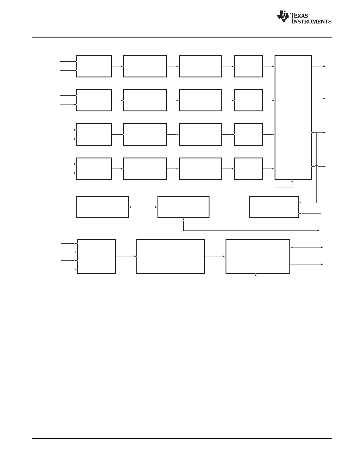
10-Bit
ADC
VIN_1_P
VIN_1_N
Y/C
Separation
Noise Reduction/
Auto Contrast
Scaler
VIN_2_P
VIN_2_N
VIN_3_P
VIN_3_N
VIN_4_P
VIN_4_N
Output
Formattor
DVO_A_[7:0]
Delay Match
and Re-Sync
Cascade
Input
ARM/Memory
Registers
I C Host port
2
Audio
ADC
AIN_1
AIN_2
AIN_3
AIN_4
Decimation Filter
and Mixer
I C
2
I S Encoder
2
Audio Cascade Input
BCLK_R
LRCLK_R
SD_R/SD_M
SD_CO
Y/C
Separation
Y/C
Separation
10-Bit
ADC
10-Bit
ADC
Y/C
Separation
10-Bit
ADC
Scaler
Scaler
Scaler
Noise Reduction/
Auto Contrast
Noise Reduction/
Auto Contrast
Noise Reduction/
Auto Contrast
DVO_B_[7:0]
DVO_C_[7:0]
DVO_D_[7:0]
TVP5158, TVP5157, TVP5156
SLES243D–JULY 2009–REVISED OCTOBER 2010
1.8 Functional Block Diagram
www.ti.com
Figure 1-1. Functional Block Diagram
12 Introduction Copyright © 2009–2010, Texas Instruments Incorporated
Submit Documentation Feedback
Product Folder Link(s): TVP5158 TVP5157 TVP5156

96
VSSA95AIN_194AIN_2
93 AIN_3
92
AIN_491VDDA_1_890VSS
89 SD_M
88
SD_R
87
VSS
86
LRCLK_R85BCLK_R
84 VDD_1_1
83
SD_CO
82
VSS81VDD_3_3
80 I2CA0
79
VSS
78
DVO_A_0
77
DVO_A_176VDD_1_1
75 DVO_A_2
74
DVO_A_373VSS
72
DVO_A_4
71 DVO_A_5
70
VDD_3_369DVO_A_6
68
DVO_A_767VDD_1_1
66 I2CA1
65
VSS
64
VDD_1_1
63
DVO_B_0
62
DVO_B_1
61 VSS
60
DVO_B_2
59
DVO_B_3
58
VDD_3_3
57 DVO_B_4
56
DVO_B_5
55
VSS
54
DVO_B_6
53 DVO_B_7
52
VDD_1_1
51
OCLK_N/CLKIN
50
OCLK_P
49 VSS
48
I2CA2
47
VSS
46
DVO_C_0
45 DVO_C_1
44
VDD_1_1
43
DVO_C_2
42
DVO_C_3
41 VDD_3_3
40
DVO_C_4
39
DVO_C_5
38
VSS
37 DVO_C_6
36
DVO_C_7
35
VDD_1_1
34
NC
33 VSS
1VSS
2
INTREQ3RESETB
4SCL
5
SDA
6
VSS
7
T1
8T2
9
T310T411T5
12
VSS
13VDD_1_1
14
VSS
15
VDD_3_3
16
LRCLK_CI
17BCLK_CI
18
VDD_1_1
19
SD_CI
20
VSS
21
DVO_D_722DVO_D_623VDD_1_124DVO_D_525DVO_D_4
26VSS
27
DVO_D_328DVO_D_229VDD_3_330DVO_D_131DVO_D_032VDD_1_1
97
OSC_OUT
98
VSSA
99XTAL_IN
100XTAL_REF
101
XTAL_OUT
102
VDDA_1_8
103VDDA_1_1
104
VSSA
105
VSSA
106VDDA_1_1
107VDDA_1_8
108VIN_1_P
109VIN_1_N
110
VSSA
111
VSSA
112VIN_2_P
113VIN_2_N
114VDDA_1_8
115VDDA_1_8
116REXT_2K
117
VSSA
118
VSSA
119VDDA_1_1
120VDDA_1_8
121VIN_3_P
122VIN_3_N
123
VSSA
124
VSSA
125VIN_4_P
126VIN_4_N
127VDDA_1_8
128VDAA_3_3
TVP5158
128-Pin TQFP Package
TVP5158, TVP5157, TVP5156
www.ti.com
2 Terminal Assignments
2.1 Pinout
SLES243D–JULY 2009–REVISED OCTOBER 2010
Copyright © 2009–2010, Texas Instruments Incorporated Terminal Assignments 13
Submit Documentation Feedback
Product Folder Link(s): TVP5158 TVP5157 TVP5156
TVP5158, TVP5157, TVP5156
SLES243D–JULY 2009–REVISED OCTOBER 2010
Table 2-1. Terminal Functions
TERMINAL
NAME NO.
Analog Section
VIN_1_P 108 I Analog video input for ADC channel 1.
VIN_1_N 109 I Common-mode reference input for ADC channel 1.
VIN_2_P 112 I Analog video input for ADC channel 2.
VIN_2_N 113 I Common-mode reference input for ADC channel 2.
VIN_3_P 121 I Analog video input for ADC channel 3.
VIN_3_N 122 I Common-mode reference input for ADC channel 3.
VIN_4_P 125 I Analog video input for ADC channel 4.
VIN_4_N 126 I Common-mode reference input for ADC channels.
REXT_2K 116 I External resistor for AFE bias generator. Connect external 1.8kΩ resistor to ground.
AIN_1 95 I Analog audio input for channel 1 (No Connect for TVP5156 Only)
AIN_2 94 I Analog audio input for channel 2 (No Connect for TVP5156 Only)
AIN_3 93 I Analog audio input for channel 3 (No Connect for TVP5156 Only)
AIN_4 92 I Analog audio input for channel 4 (No Connect for TVP5156 Only)
XTAL_IN 99 I
XTAL_REF 100 G Crystal reference. Connected to analog ground internally.
XTAL_OUT 101 O
Analog Power
VDDA_1_1 103, 106, 119 P 1.1V analog supply
VDDA_1_8 114, 115, 120, P 1.8V analog supply
VDDA_3_3 128 P 3.3V analog supply for all 4 video channels
VSSA G Analog ground
Digital Power
VSS 49, 55, 61, 65, G Digital ground
VDD_1_1 35, 44, 52, 64, P Digital core supply. Connect to 1.1-V digital supply.
VDD_3_3 P Digital I/O supply. Connect to 3.3-V digital supply.
Digital Section
INTREQ 2 O Interrupt request. Interrupt signal to host processor.
RESETB 3 I Reset. An active low signal that controls the reset state.
SCL 4 I/O I2C serial clock (open drain)
SDA 5 I/O I2C serial data (open drain)
OSC_OUT 97 O Buffered crystal oscillator output. 1.8-V compatible.
OCLK_P 51 O Output data clock+. All 4 digital video output ports are synchronized to this clock.
OCLK_N/CLKIN 50 I/O
DVO_A_[7:0] O Digital video output data bus.
91, 102, 107,
127
96, 98, 104,
105, 110, 111,
117, 118, 123,
124
1, 6, 12, 14, 20,
26, 33, 38, 47,
73, 79, 82, 87,
90
13, 18, 23, 32,
67, 76, 84
15, 29, 41, 58,
70, 81
68, 69, 71, 72,
74, 75, 77, 78
I/O DESCRIPTION
External clock reference input. It may be connected to external oscillator with 1.8-V compatible
clock signal or 27.0-MHz crystal oscillator.
External clock reference output. Not connected if XTAL_IN is driven by an external
single-ended oscillator.
Output data clock- for 2-Ch time-multiplexed mode or data clock input for 8-Ch video cascade
mode
www.ti.com
14 Terminal Assignments Copyright © 2009–2010, Texas Instruments Incorporated
Submit Documentation Feedback
Product Folder Link(s): TVP5158 TVP5157 TVP5156
TVP5158, TVP5157, TVP5156
www.ti.com
SLES243D–JULY 2009–REVISED OCTOBER 2010
Table 2-1. Terminal Functions (continued)
TERMINAL
NAME NO.
DVO_B_[7:0] O Digital video output data bus.
DVO_C_[7:0] I/O
DVO_D_[7:0] I/O
I2CA0 80 I I2C slave address bit 0
I2CA1 66 I I2C slave address bit 1
I2CA2 48 I I2C slave address bit 2
Digital Audio Section (Not supported on TVP5156)
BCLK_R 85 I/O
LRCLK_R 86 I/O
SD_R 88 O I2S serial data output for recording.
SD_M 89 O I2S serial data output for mixed audio or recording.
SD_CO 83 O Audio serial data output for cascade mode
LRCLK_CI 16 I I2S left/right clock input for cascade mode. Also known as I2S word select (WS).
BCLK_CI 17 I I2S bit clock input for cascade mode. Also known as I2S serial clock (SCK).
SD_CI 19 I Audio serial data input for cascade mode.
No Connect Pins
T1, T2, T3, T4, 7, 8, 9, 10, 11,
T5, NC 34
53, 54, 56, 57,
59, 60, 62, 63
36, 37, 39, 40, Digital video output data bus. In cascade mode, all pins operate as input from another
42, 43, 45, 46 TVP5158 device.
21, 22, 24, 25, Digital video output data bus. In cascade mode, all pins operate as input from another
27, 28, 30, 31 TVP5158 device.
I/O DESCRIPTION
I2S bit clock for recording. Also known as I2S serial clock (SCK). Supports master and slave
modes.
I2S left/right clock for recording. Also known as I2S word select (WS). Supports master and
slave modes.
NC For normal operation, no connect
Copyright © 2009–2010, Texas Instruments Incorporated Terminal Assignments 15
Submit Documentation Feedback
Product Folder Link(s): TVP5158 TVP5157 TVP5156
Anti-Aliasing
Filter
Analog
CVBS Input
Clamp
ADC
Reference & Bias
Output to
Digital
Processing
Frequency Response
-35
-30
-25
-20
-15
-10
-5
0
5
- 5 1 0 1 5 2 0 25
Freq uency ( MHz)
Gain(dB)
TVP5158, TVP5157, TVP5156
SLES243D–JULY 2009–REVISED OCTOBER 2010
3 Functional Description
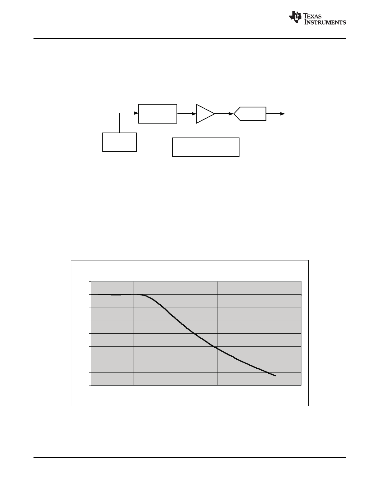
3.1 Analog Video Processing and A/D Converters
Each video decoder accepts one composite video input and performs video clamping, anti-aliasing
filtering, video amplification, A/D conversion, and gain and offset adjustments to center the digitized video
signal. Figure 3-1 shows the video analog processing and ADC block diagram.
Figure 3-1. Video Analog Processing and ADC Block Diagram
3.1.1 Analog Video Input
Supports NTSC (J, M, 4.43) and PAL (B, D, G, H, I, M, N, Nc, 60) video standards. Each video decoder
channel supports a composite video input with a pseudo-differential pin which improves the noise
immunity and analog performance.
www.ti.com
Each video decoder input should be ac-coupled through a 0.1-µF capacitor. The nominal parallel
termination resistor before the input to the device is 75 Ω.
Each video decoder integrates an anti-aliasing filter to provide good stop-band rejection on the analog
video input signal. Figure 3-2 shows the frequency response of the anti-aliasing filter.
Figure 3-2. Anti-Aliasing Filter Frequency Response
16 Functional Description Copyright © 2009–2010, Texas Instruments Incorporated
Submit Documentation Feedback
Product Folder Link(s): TVP5158 TVP5157 TVP5156

TVP5158, TVP5157, TVP5156
www.ti.com
3.1.2 Analog Video Input Clamping
An internal clamping circuit provides dc restoration for all four analog composite video inputs. The dc
restoration circuit (sync-tip clamp) restores sync-tip level of the ac-coupled composite video signal to a
fixed dc level near the bottom of the A/D converter range.
3.1.3 A/D Converter
All ADCs have a resolution of 10 bits and can operate at 27 MSPS. Each A/D channel receives a clock
from the on-chip phase-locked loop (PLL) at a nominal frequency of 27 MHz. All ADC reference voltages
are generated internally.
3.2 Digital Video Processing
Digital Video Processing block receives digitized video signals from the ADCs and performs composite
processing and YCbCr signal enhancements. The digital data output can be programmed to two formats:
ITU-R BT.656 8-bit 4:2:2 with embedded syncs or 16-bit 4:2:2 with embedded syncs. The circuit also
detects pseudo-sync pulses, AGC pulses, and color striping in Macrovision-encoded copy-protected
material.
3.2.1 2x Decimation Filter
All input signals are over-sampled by a factor of 2 (by 27-MHz clock). The A/D outputs initially pass
through decimation filters that reduce the data rate to 1x the pixel rate. The decimation filter is a half-band
filter. Over-sampling and decimation filtering can effectively increase the overall signal-to-noise ratio by
3 dB.
SLES243D–JULY 2009–REVISED OCTOBER 2010
3.2.2 Automatic Gain Control
The automatic gain control (AGC) can be enabled and can adjust the signal amplitude controlled by 14-bit
digital gain stage after the ADC. The AGC algorithms can use up to four amplitude references: sync
height, color burst amplitude, composite peak, and luma peak.
The specific amplitude references being used by the AGC algorithms can be controlled using the AGC
white peak processing register located at sub-address 2Dh. The gain increment speed and gain increment
delay can be controlled using the AGC increment speed register located at sub-address 29h and the AGC
increment delay register located at sub-address 2Ah. The gain decrement speed and gain decrement
delay can be controlled using the AGC decrement speed register located at sub-address 2Bh and the
AGC decrement delay register located at sub-address 2Ch.
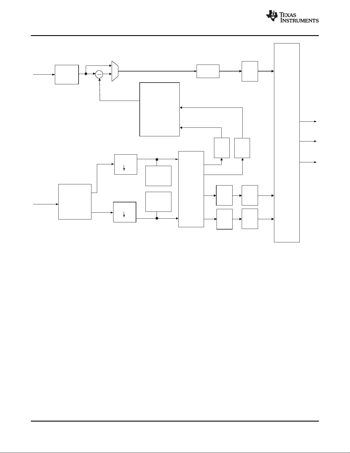
3.2.3 Composite Processor
This Composite Processor circuit receives a digitized composite signal from the ADCs and performs sync
and Y/C separation, chroma demodulation for PAL/NTSC, and YUV signal enhancements. The slice levels
of the sync separator are adaptive. The slice levels continually adapt to changes in the back-porch and
sync-tip levels. The 10-bit composite video is multiplied by the sub carrier signals in the quadrature
demodulator to generate U and V color difference signals. The U and V signals are then sent to low-pass
filters to achieve the desired bandwidth. An adaptive 5-line comb filter separates UV from Y based on the
unique property of color phase shifts from line to line. The chroma is re-modulated through a quadrature
modulator and subtracted from line-delayed composite video to generate luma. This form of Y/C
separation is completely complementary, thus there is no loss of information. However, in some
applications, it is desirable to limit the U/V bandwidth to avoid crosstalk. In that case, notch filters can be
turned on. To accommodate some viewing preferences, a peaking filter is also available in the luma path.
Contrast, brightness, sharpness, hue, and saturation controls are programmable through the I2C host port.
Figure 3-3 shows the block diagram of Composite Processor.
Copyright © 2009–2010, Texas Instruments Incorporated Functional Description 17
Submit Documentation Feedback
Product Folder Link(s): TVP5158 TVP5157 TVP5156
Color LPF
2
5 Line
Adaptive
Comb Filter
Notch
Filter
Notch
Filter
Delay
Delay
Contrast
Brightness
Saturation
Adjust
Color LPF
2
Y
Cb
Cr
U
V
Notch
Notch
Delay
Y
Peaking
NTSC/PAL
Remodulation
NTSC/PAL
Demodulation
Line
Delay
CVBS
CVBS
Burst
Accumulator
(U)
Burst
Accumulator
(V)
Filter
Filter
TVP5158, TVP5157, TVP5156
SLES243D–JULY 2009–REVISED OCTOBER 2010
www.ti.com
Figure 3-3. Composite Processor Block Diagram
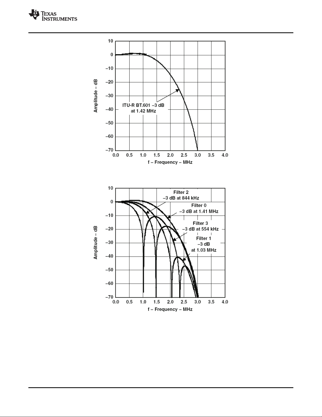
3.2.3.1 Color Low-Pass Filter
High filter bandwidth preserves sharp color transitions and produces crisp color boundaries. However, for
nonstandard video sources that have asymmetrical U and V side bands, it is desirable to limit the filter
bandwidth to avoid UV crosstalk. The color low-pass filter bandwidth is programmable to enable one of the
three notch filters. Figure 3-4 and Figure 3-5 represent the frequency responses of the wideband color
low-pass filters.
18 Functional Description Copyright © 2009–2010, Texas Instruments Incorporated
Product Folder Link(s): TVP5158 TVP5157 TVP5156
Submit Documentation Feedback
TVP5158, TVP5157, TVP5156
www.ti.com
SLES243D–JULY 2009–REVISED OCTOBER 2010
Figure 3-4. Color Low-Pass Filter Frequency Response
Figure 3-5. Color Low-Pass Filter with Filter Characteristics, NTSC/PAL ITU-R BT.601 Sampling
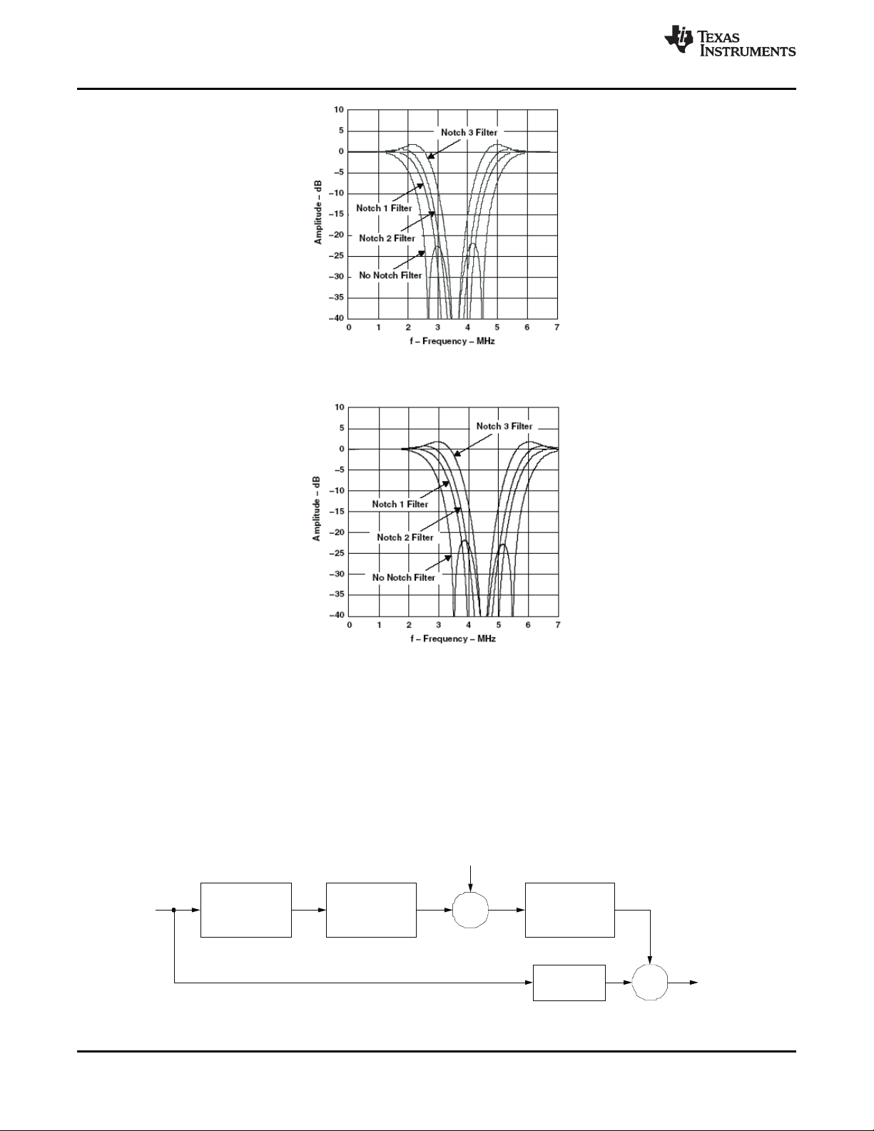
3.2.3.2 Y/C Separation
Y/C separation can be done using adaptive 5-line (5-H delay) comb filters or a chroma trap filter. The
comb filter can be selectively bypassed in the luma or chroma path. If the comb filter is bypassed in the
luma path, then chroma trap filters are used which are shown in Figure 3-6 and Figure 3-7. The TI
patented adaptive comb filter algorithm reduces artifacts such as hanging dots at color boundaries. It
detects and properly handles false colors in high-frequency luminance images such as a multiburst pattern
or circle pattern.
Copyright © 2009–2010, Texas Instruments Incorporated Functional Description 19
Submit Documentation Feedback
Product Folder Link(s): TVP5158 TVP5157 TVP5156
Peak
Detector
Bandpass
Filter
Peaking
Filter
Delay
IN
Gain
OUT
+
x
TVP5158, TVP5157, TVP5156
SLES243D–JULY 2009–REVISED OCTOBER 2010
Figure 3-6. Chroma Trap Filter Frequency Response, NTSC ITU-R BT.601 Sampling
www.ti.com
Figure 3-7. Chroma Trap Filter Frequency Response, PAL ITU-R BT.601 Sampling
3.2.4 Luminance Processing
The digitized composite video signal passes through either a luminance comb filter or a chroma trap filter,
either of which removes chrominance information from the composite signal to generate a luminance
signal. The luminance signal is then fed into the input of a peaking circuit. Figure 3-8 shows the basic
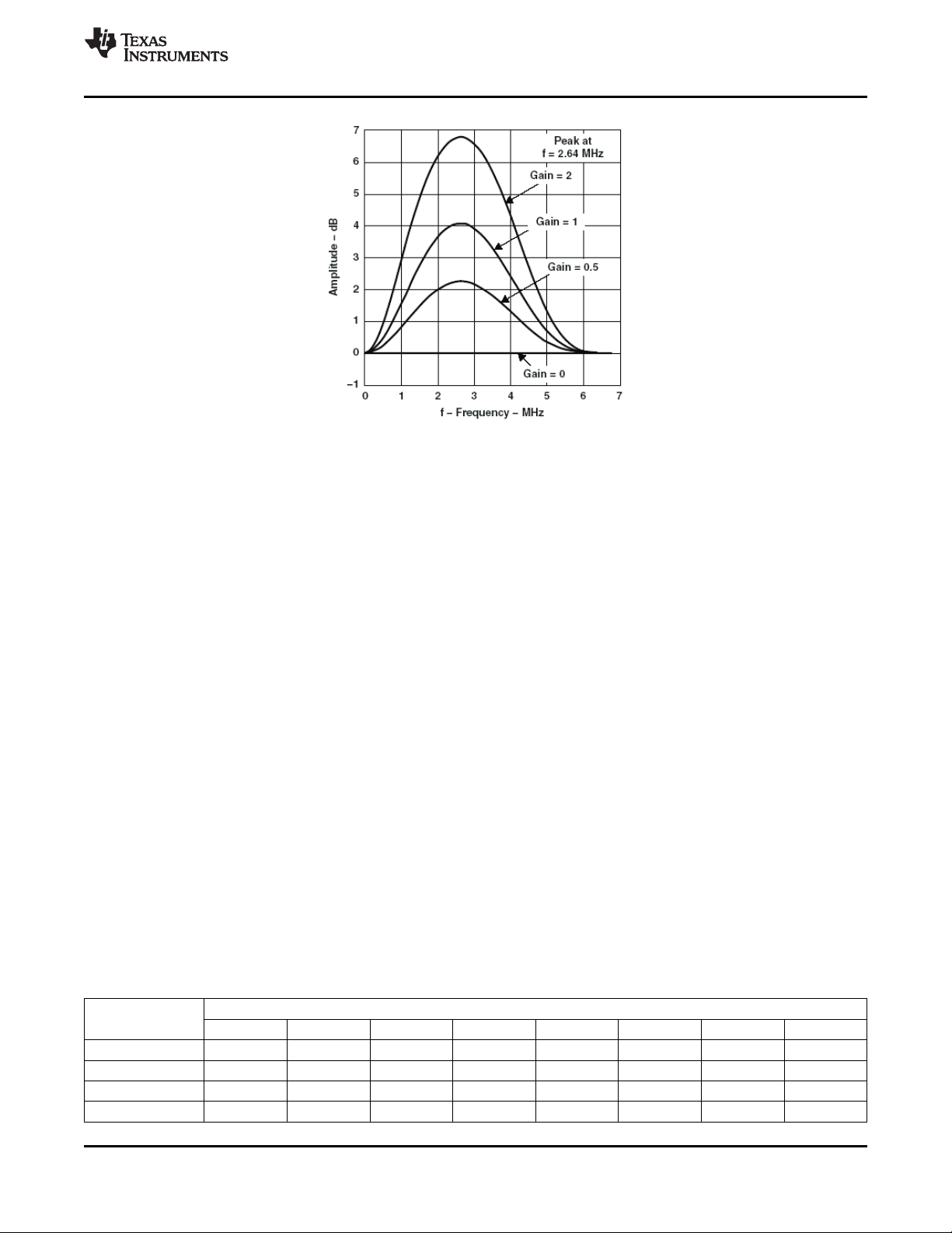
functions of the luminance data path. A peaking filter (edge enhancer) amplifies high-frequency
components of the luminance signal. Figure 3-9 shows the characteristics of the peaking filter at four
different gain settings that are user-programmable via the I2C interface.
20 Functional Description Copyright © 2009–2010, Texas Instruments Incorporated
Figure 3-8. Luminance Edge-Enhancer Peaking Block Diagram
Submit Documentation Feedback
Product Folder Link(s): TVP5158 TVP5157 TVP5156
TVP5158, TVP5157, TVP5156
www.ti.com
Figure 3-9. Peaking Filter Response, NTSC/PAL ITU-R BT.601 Sampling
3.3 AVID Cropping
AVID or active video cropping provides a means to decrease the amount of video data output. This is
accomplished by horizontally blanking a number of AVID pulses and by vertically blanking a number of
lines per frame. Horizontal cropping can be enabled/disabled using bit-6 of address B1h. When line
cropping is enabled, active video will be reduced from 720 to 704 pixels for unscaled video and from 360
to 352 pixels for down-scaled video.
SLES243D–JULY 2009–REVISED OCTOBER 2010
When line cropping is enabled, the TVP5158 crops an equal amount from both the start and end of active
video. Register 8Ch can be used to delay both the start and end of active video. It allows selecting which
704 pixels out of 720 are actually being used for active video when line cropping is enabled.
3.4 Embedded Syncs
Standards with embedded syncs insert SAV and EAV codes into the data stream at the beginning and end
of horizontal blanking. These codes contain the V and F bits which also define vertical timing. F and V
change on EAV. Table 3-1 gives the format of the SAV and EAV codes.
H equals 1 always indicates EAV. H equals 0 always indicates SAV. The alignment of V and F to the line
and field counter varies depending on the standard. Please refer to ITU-R BT.656 for more information on
embedded syncs.
The P bits are protection bits:
P3 = V xor H
P2 = F xor H
P1 = F xor V
P0 = F xor V xor H
Table 3-1. EAV and SAV Sequence
8-BIT DATA
D7 (MSB) D6 D5 D4 D3 D2 D1 D0
Preamble 1 1 1 1 1 1 1 1
Preamble 0 0 0 0 0 0 0 0
Preamble 0 0 0 0 0 0 0 0
Status word 1 F V H P3 P2 P1 P0
Copyright © 2009–2010, Texas Instruments Incorporated Functional Description 21
Submit Documentation Feedback
Product Folder Link(s): TVP5158 TVP5157 TVP5156
TVP5158, TVP5157, TVP5156
SLES243D–JULY 2009–REVISED OCTOBER 2010
3.5 Scaler
Each video decoder has an independent horizontal and vertical scaler, which supports D1 to half-D1 or
CIF conversion. Table 3-2 gives the details of video resolution including un-cropped and cropped.
Table 3-3 shows the video resolutions converted by the scaler.
Table 3-2. Standard Video Resolutions
Format
D1 720 x 480 720 x 576 704 x 480 704 x 576
Half-D1 360 x 480 360 x 576 352 x 480 352 x 576
CIF 360 x 240 360 x 288 352 x 240 352 x 288
Table 3-3. Video Resolutions Converted by the Scaler
Scaling Ratio Format Horizontal Scaling Vertical Scaling Total Pixel
D1
D1 to Half-D1
D1 to CIF
NTSC 1:1 1:1 858 x 525 720 x 480
PAL 1:1 1:1 864 x 625 720 x 576
NTSC 2:1 1:1 429 x 525 360 x 480
PAL 2:1 1:1 432 x 625 360 x 576
NTSC 2:1 2:1 429 x 262 360 x 240
PAL 2:1 2:1 432 x 312 360 x 288
Uncropped Cropped
NTSC PAL NTSC PAL
www.ti.com
Active Output
Resolution
3.6 Noise Reduction
A video sequence shot under low light condition, which is typical of video surveillance applications, can
contain lots of noise. Human eyes are very sensitive to oscillating signals, the visual quality degenerates
significantly even when the noise level is small.
Each video decoder uses a TI proprietary spatial filter to reduce video noise. For each frame of image, the
video noise filter (VNF) produces an estimate of the Y/U/V noise. Based on the noise estimates, the
firmware adjusts the threshold for Y/U/V filtering. The filtered video shows improved video quality and
lower compression bit-rate. The firmware can also utilize the Y/U/V noise estimates to make decisions to
disable color if the video noise is determined to be too high. This "color killer" decision bit can be used to
control another module that implements the color killing function.
The Noise Reduction can be controlled using I2C registers from 50h to 5Fh. This module can also be set
to bypass mode by I2C register 5Dh (Bit 0).
3.7 Auto Contrast
The Auto Contrast (AC) module can adjust the picture brightness automatically or manually (user
programmable) for better image quality. The goal of AC processing is to make the dark area brighter and
high-light area dimmer. This makes it possible for the viewer to see details hidden in the shadows. It also
prevents loss of details in the washed-out high light area. The AC processing is mostly for video
surveillance applications.
For each frame of image, the auto contrast module collects the statistics of its Y (luminance) values. The
AC algorithm implemented in the firmware processes the statistics and generates a look-up table (LUT).
This LUT is used to map each incoming pixel Y value to an output pixel Y value for the next frame of
image. The LUT is updated during the blanking period between two frames.
The Auto Contrast Mode can be controlled by using I2C registers 0Fh. This module can also be set to
disable mode by I2C register 0Fh (Bit 1:0).
22 Functional Description Copyright © 2009–2010, Texas Instruments Incorporated
Submit Documentation Feedback
Product Folder Link(s): TVP5158 TVP5157 TVP5156
TVP5158, TVP5157, TVP5156
www.ti.com
SLES243D–JULY 2009–REVISED OCTOBER 2010
3.8 Output Formatter
The output formatter is responsible for generating the output digital video stream. Table 3-4 provides a
summary of line frequencies, data rates, and pixel counts for different input standards. TVP5158 supports
non-interleaved output mode, pixel-interleaved output mode and line-interleaved output mode. The
non-interleaved mode is similar to the TVP5154A device, except that a single fixed clock output is used. In
the interleaved modes, the video output data from multiple decoder channels are multiplexed together and
then output to a single 8-bit or 16-bit port. The video output data from selected channels can be
interleaved on a pixel or line basis.
Table 3-4. Summary of Line Frequencies, Data Rates and Pixel Counts for Different Standards
Standards Active Pixels Lines per
(ITU-R BT.601) per Line Frame
NTSC-J, M 858 720 525 13.5 3.579545 15.73426
NTSC-4.43 858 720 525 13.5 4.43361875 15.73426
PAL-M 858 720 525 13.5 3.57561149 15.73426
PAL-60 858 720 525 13.5 4.43361875 15.73426
PAL-B, D, G, H, I 864 720 625 13.5 4.43361875 15.625
PAL-N 864 720 625 13.5 4.43361875 15.625
PAL-Nc 864 720 625 13.5 3.58205625 15.625
Pixels per Line Frequency Frequency Rate
Pixel Color Subcarrier Horizontal Line
(MHz) (MHz) (kHz)
3.8.1 Non-Interleaved Mode
In the non-interleaved mode, the YCbCr digital output is programmed as 8-bit ITU-R BT.656 parallel
interface standard. Depending on which output mode is selected, the output for each channel can be
un-scaled data or scaled data. Also each video output port can be selected to output the video data from
any 1 of 4 video decoders. Table 3-5 shows the detailed information about non-interleaved mode.
Table 3-5. Output Ports Configuration for Non-Interleaved Mode
Video Output Cascade I2C Address: OCLK
Format Stage B0h (MHz)
1-Ch D1 n/a 00h 27 Any 1 of 4 Ch Any 1 of 4 Ch Any 1 of 4 Ch Any 1 of 4 Ch
1-Ch Half-D1 n/a 02h 27 Any 1 of 4 Ch Any 1 of 4 Ch Any 1 of 4 Ch Any 1 of 4 Ch
1-Ch CIF n/a 03h 27 Any 1 of 4 Ch Any 1 of 4 Ch Any 1 of 4 Ch Any 1 of 4 Ch
Port A Port B Port C Port D
3.8.2 Pixel-Interleaved Mode
Each video decoder supports multiplexing two or four channels ITU-R BT.656 format data together on a
pixel basis. The output from each video decoder channel is still ITU-R BT.656 format. After the processing
in output formatter, two or four channels video data has been interleaved together by strictly one pixel
from each channel.
The pixel-interleaved mode is dedicated for the backend chip which has limited video input ports.
Table 3-6 gives the output port configuration for pixel-interleaved mode.
Copyright © 2009–2010, Texas Instruments Incorporated Functional Description 23
Submit Documentation Feedback
Product Folder Link(s): TVP5158 TVP5157 TVP5156
FF 00 Y0 Y1 Y2 Y3
CLK_P
(27MHz)
CH1_D
00 XY
CH2_D
DVO_A_
[7:0]
Cb0 C r0 Cb2 Cr2
Cb20 Y20 Cr 20 Y21 Cb22 Y22 C r22 Y23 Cb 24 Y24 Cr24 Y25
FF 00 Y0 Y1 Y2 Y300 XY Cb0 C r0 Cb2 Cr2Cb20 Y20 Cr 20 Y21 Cb22 Y22 C r22 Y23 Cb 24 Y24 Cr24 Y25
CLK_N
(27MHz)
FF 00 Y0
CLK (108MHz)
CH1_D
00 XY
CH2_D
Cb0
Cr50 Cb52 Cr52
Cb20 Y20 Cr20 Y21
Cb22 Y22
Cr92 Y93 Cb94 Y94
Cr 94
Y95
Y51 Y52 Y53
FF 00 Y000 XY Cb0Cb20 Y 20 Cr20 Y21 C b22 Y22Cr50 Cb52 Cr52Y51 Y52 Y53Cr92 Y93 Cb94 Y94
Cr 94
Y95
CH3_D
CH4_D
DVO_A_
[7:0]
TVP5158, TVP5157, TVP5156
SLES243D–JULY 2009–REVISED OCTOBER 2010
Table 3-6. Output Ports Configuration for Pixel-Interleaved Mode
Video Output Cascade I2C Address: OCLK
Format Stage B0h (MHz)
2-Ch D1 n/a 50h 54 Any 2 of 4 Ch Any 2 of 4 Ch Hi-Z Hi-Z
4-Ch D1 n/a 60h 108 All 4 Ch Hi-Z Hi-Z Hi-Z
4-Ch Half-D1 n/a 62h 54 All 4 Ch Hi-Z Hi-Z Hi-Z
4-Ch CIF n/a 63h 54 All 4 Ch Hi-Z Hi-Z Hi-Z
Port A Port B Port C Port D
3.8.2.1 2-Ch Pixel-Interleaved Mode
In 2-Ch pixel-interleaved mode, the video output data with D1 resolution from two video channels is
multiplexed pixel by pixel at 54 MHz. The output ports DVO_A and DVO_B are used in this mode. The
output clocks OCLK_P and OCLK_N are synchronized with each channel so that the backend chip can
de-multiplexed each video channel data easily. The video output from each channel is compatible with
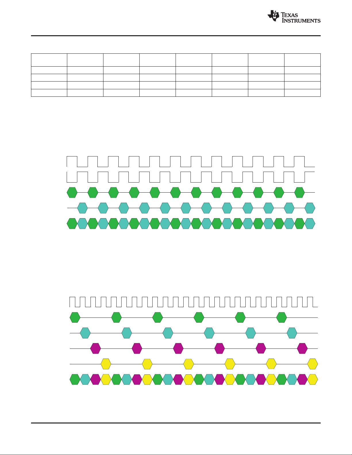
ITU-R BT.656 format. Figure 3-10 shows the timing diagram for 2-Ch pixel-interleaved mode.
www.ti.com
Figure 3-10. 2-Ch Pixel-Interleaved Mode Timing Diagram
3.8.2.2 4-Ch Pixel-Interleaved Mode
In 4-Ch pixel-interleaved mode, the video output data with D1 resolution from four video channels is
multiplexed pixel by pixel at 108 MHz. The output DVO_A is used in this mode. The output clock OCLK_P
is synchronized with all four channels data. Each channel video data is compatible with ITU-R BT.656
format. Figure 3-11 shows the timing diagram for 4-Ch pixel-interleaved mode.
Figure 3-11. 4-Ch Pixel-Interleaved Mode Timing Diagram
24 Functional Description Copyright © 2009–2010, Texas Instruments Incorporated
Submit Documentation Feedback
Product Folder Link(s): TVP5158 TVP5157 TVP5156

TVP5158, TVP5157, TVP5156
www.ti.com
SLES243D–JULY 2009–REVISED OCTOBER 2010
In 4-Ch pixel-interleaved mode, TVP5158 also supports Half-D1 and CIF format data multiplexed at 54
MHz. The output DVO_A is used in this mode. The output clock OCLK_P is synchronized with all four
channels data.
3.8.2.3 Metadata Insertion for Non-Interleave Mode and Pixel-Interleaved Mode
In non-interleaved mode and pixel-interleaved mode, the video detection status (VDET) has also been
inserted in MSB of SAV/EAV control byte. Table 3-7 shows VDET status insertion in SAV/EAV codes.
Table 3-7. VDET Statues Insertion in SAV/EAV Codes
CONDITION FVH VALUE SAV/EAV CODE SEQUENCE
FIELD V TIME H TIME F V H 1st 2nd 3rd
1 Active SAV 0 0 0 FFh 00h 00h 80h 00h
1 Active EAV 0 0 1 FFh 00h 00h 9Dh 1Dh
1 Blank SAV 0 1 0 FFh 00h 00h ABh 2Bh
1 Blank EAV 0 1 1 FFh 00h 00h B6h 36h
2 Active SAV 1 0 0 FFh 00h 00h C7h 47h
2 Active EAV 1 0 1 FFh 00h 00h DAh 5Ah
2 Blank SAV 1 1 0 FFh 00h 00h ECh 6Ch
2 Blank EAV 1 1 1 FFh 00h 00h F1h 71h
VDET = 1 VDET = 0
4th
In the pixel-interleaved mode, Channel ID is inserted in the horizontal blanking code as Table 3-8. The
backend chip can easily identify the video data from which video decoder channel by inserted Channel ID.
Table 3-8. Channel ID Insertion in Horizontal Blanking Code
CHANNEL
Ch1 10h 80h 80h
Ch2 11h 81h 81h
Ch3 12h 82h 82h
Ch4 13h 83h 83h
H BLANKING CODE WITH CHANNEL ID
Y Cb Cr
In the pixel-interleaved mode, Channel ID can also be inserted in 4 LSBs of SAV/EAV control byte
replacing protection bits as Table 3-9.
Table 3-9. Channel ID Insertion in SAV/EAV Code Sequence
CONDITION FVH VALUE SAV/EAV CODE SEQUENCE
FIELD V TIME H TIME F V H 1st 2nd 3rd
1 Active SAV 0 0 0 FFh 00h 00h 80h 81h 82h 83h
1 Active EAV 0 0 1 FFh 00h 00h 90h 91h 92h 93h
1 Blank SAV 0 1 0 FFh 00h 00h A0h A1h A2h A3h
1 Blank EAV 0 1 1 FFh 00h 00h B0h B1h B2h B3h
2 Active SAV 1 0 0 FFh 00h 00h C0h C1h C2h C3h
2 Active EAV 1 0 1 FFh 00h 00h D0h D1h D2h D3h
2 Blank SAV 1 1 0 FFh 00h 00h E0h E1h E2h E3h
2 Blank EAV 1 1 1 FFh 00h 00h F0h F1h F2h F3h
Ch1 Ch2 Ch3 Ch4
4th
Copyright © 2009–2010, Texas Instruments Incorporated Functional Description 25
Submit Documentation Feedback
Product Folder Link(s): TVP5158 TVP5157 TVP5156
TVP5158, TVP5157, TVP5156
SLES243D–JULY 2009–REVISED OCTOBER 2010
3.8.3 Line-Interleaved Mode Support (TVP5158 only)
The TVP5158 supports 2-Ch, 4-Ch, and 8-Ch line-interleaved modes. In the line-interleaved mode, the
video channels are multiplexed together on a line-by-line basis. Compared to the pixel-interleaved mode,
the line-interleaved mode significantly reduces the code complexity and MIPS consumption of the backend
processor. The 8-Ch modes require connecting two TVP5158 devices together using a video cascade
interface (see Section 3.8.3.3). The TVP5158 also supports different image resolutions (for example, D1,
Half-D1, and CIF) in the line-interleaved mode. All supported line-interleaved modes are shown in
Table 3-10.
Table 3-10. Output Ports Configuration for Line-Interleaved Mode
Video Output Cascade I2C Address: OCLK
Format Stage B0h (MHz)
2-Ch D1 n/a 90h 54 Any 2 of 4 Ch Any 2 of 4 Ch Hi-Z Hi-Z
4-Ch D1 n/a A0h 108 All 4 Ch Hi-Z Hi-Z Hi-Z
4-Ch Half-D1 n/a A2h 54 All 4 Ch Hi-Z Hi-Z Hi-Z
4-Ch CIF n/a A3h 27 All 4 Ch Hi-Z Hi-Z Hi-Z
4-Ch D1 All 4 Ch All 4 Ch
(16-bit) (Y data) (C data)
4-Ch Half-D1 All 4 Ch All 4 Ch
(16-bit) (Y data) (C data)
8-Ch Half-D1
8-Ch CIF
4-Ch Half-D1 + 4 Ch Half-D1 +
1-Ch D1 Any 1 of 4 D1
4-Ch CIF + 4-Ch CIF + Any
1-Ch D1 1 of 4 D1
8-Ch CIF +
1-Ch D1
n/a A8h 54 Hi-Z Hi-Z
n/a AAh 27 Hi-Z Hi-Z
1st B2h 108 Hi-Z Hi-Z
2nd B6h 54 Hi-Z Hi-Z Hi-Z
1st B3h 54 Hi-Z Hi-Z 4-Ch CIF Input
2nd B7h 27 Hi-Z Hi-Z Hi-Z
n/a E2h 108 Hi-Z Hi-Z Hi-Z
n/a E3h 54 Hi-Z Hi-Z Hi-Z
1st F3h 108 Hi-Z 1-Ch D1 Input 4-Ch CIF Input
2nd F7h 27 1-Ch D1 Output Hi-Z Hi-Z
Port A Port B Port C Port D
8-Ch Half-D1 4-Ch Half-D1
Output Input
4-Ch Half-D1
Output
8-Ch CIF
Output
4-Ch CIF
Output
8-Ch CIF + Any
1 of 8 D1
4-Ch CIF
Output
www.ti.com
3.8.3.1 2-Ch Line-Interleaved Mode
TVP5158 supports 2-Ch line-interleaved mode at 54 MHz. The video output data with D1 resolution from
any two video channels is multiplexed together on a line basis. The output ports DVO_A and DVO_B are
used in this mode. The output clock OCLK_P is synchronized with both output ports.
3.8.3.2 4-Ch Line-Interleaved Mode
In 4-Ch line-interleaved mode, the video output data from all 4 channels is multiplexed together on a line
basis. The output resolution of video data can be D1, Half-D1 or CIF. For D1 and Half-D1 output
resolutions, the video output port can be configured to support 8-bit BT.656 or 16-Bit YCbCr 4:2:2 data
with embedded sync. Port DVO_A is used for 8-bit output. Ports DVO_A and DVO_B are used for 16-Bit
output. The output clock OCLK_P is synchronized with all four output ports.
TVP5158 supports multiplexing 4-Ch CIF and 1-Ch D1 data together and then output through DVO_A at
54 MHz. 1-Ch D1 can be from any one of 4 video channels. In typical surveillance applications, CIF
resolution is used for recording and D1 resolution is used for video preview.
26 Functional Description Copyright © 2009–2010, Texas Instruments Incorporated
Submit Documentation Feedback
Product Folder Link(s): TVP5158 TVP5157 TVP5156
DM6467
DaVinci HD
DVO_A_[7:0]
VPIF_A
I2C
H.264
DVO_D_[7:0]
4-C h CIF
8Bit@27MHz
8Bit@54MH z
DVO_A_[7:0]
VPIF_B
8-C h CIF
Multi-C h CIF
Preview
16-Ch CIF Recording
TVP5158
TVP5158
OCLK_P
OCLKN/CLKIN
OCLK_P
DVO_A_[7:0]
DVO_D_[7:0]
4-C h CIF
8Bit@ 27MHz
8Bit @54MH z
DVO_A_[7:0]
8-C h CIF
OCLK_P
OCLKN/CLKIN
OCLK_P
I2C
TVP5158
TVP5158
VIN_1
VIN_2
VIN_3
VIN_4
VIN_1
VIN_2
VIN_3
VIN_4
VIN_1
VIN_2
VIN_3
VIN_4
VIN_1
VIN_2
VIN_3
VIN_4
TVP5158, TVP5157, TVP5156
www.ti.com
TVP5158 also supports multiplexing 4-Ch Half-D1 and 1-Ch D1 data together and then output through
DVO_A at 108 MHz. The backend chip can use Half-D1 to generate CIF format by dropped one field.
Pleas note that the line-interleaved mode does NOT strictly output one line from each decoder channel
sequentially. The order of multiplexed the video line data is based on the availability of video output data
from each decoder channel. Therefore, it is possible to output two consecutive lines from the same
decoder channel or to skip one decoder channel output.
3.8.3.3 8-Ch Line-Interleaved Mode
Two TVP5158 devices can be cascade connected and work as single 8-Ch video decoder. In cascade
mode, the port DVO_C and DVO_D of master TVP5158 (first stage) can be configured as the video input
interface. The DVO_A and DVO_B of master TVP5158 are configured as the output interface for two
devices. This mode is dedicated for the backend chip with extremely limited input ports.
In the video cascade mode, the open-drain interrupt request (INTREQ) outputs from the first and second
stages can be combined using a wired-OR connection.
Typical applications with cascade mode show in the following diagrams.
Figure 3-12 shows the Cascade Connection for 16-Ch CIF Recoding and Multi-Ch CIF Preview.
Figure 3-13 shows the Cascade Connection for 16-Ch CIF Recoding and Multi-Ch Half-D1 Preview.
Figure 3-14 shows the Cascade Connection for 16-Ch CIF Recoding and 2-Ch D1/Multi-Ch CIF
Preview.
SLES243D–JULY 2009–REVISED OCTOBER 2010
Figure 3-12. Cascade Connection for 16-Ch CIF Recoding and Multi-Ch CIF Preview
Copyright © 2009–2010, Texas Instruments Incorporated Functional Description 27
Submit Documentation Feedback
Product Folder Link(s): TVP5158 TVP5157 TVP5156
DM6467
DaVinci HD
DVO_A_[7:0]
VPIF_A
I2C
H.264
DVO_D_[7:0]
4-Ch H alf-D1
8Bit@54MHz
8Bit@108MHz
DVO_A_[7:0]
VPIF_B
8-Ch Half-D1
Multi-Ch H alf-D1
Preview
16 -Ch CIF R ecording
TVP5158
TVP5158
OCLK_P
OCLKN/CLKIN
OCLK_P
DVO_A_[7:0]
DVO_D_[7:0]
4-Ch H alf- D1
8Bit@ 54MHz
8Bit@ 108MHz
DVO_A_[7:0]
8-Ch Half-D1
OCLK_P
OCLKN/CLKIN
OCLK_P
I2C
TVP5158
TVP5158
VIN_1
VIN_2
VIN_3
VIN_4
VIN_1
VIN_2
VIN_3
VIN_4
VIN_1
VIN_2
VIN_3
VIN_4
VIN_1
VIN_2
VIN_3
VIN_4
1-Ch D1
8Bit@27MH z
8-Ch C IF + 1 -Ch D 1
8Bit@108MHz
2-Ch D 1/M ulti-Ch CIF
Preview
DM6467
DaVinci HD
DVO_A_[7:0]
VPIF_A
I2C
H.264
DVO_D_[7:0]
DVO_A_[7:0]
VPIF_B
16 -C h C IF Rec ording
TVP5158
TVP5158
OCLK_P
OCLKN/CLKIN
OCLK_P
DVO _C _[7:0]
DVO_B_[7:0]
4-C h C IF
8Bit@ 27M Hz
8Bit@27MH z
8Bit@108MHz
DVO_A_[7:0]
I2C
DVO_D_[7:0]
DVO_A_[7:0]
TVP5158
TVP5158
OCLK_P
OCLKN/CLKIN
OCLK_P
DVO _C _[7:0]
DVO_B_[7:0]
8Bit@ 27M Hz
8-C h C IF + 1 -C h D 1
4-Ch C IF
1-Ch D 1
VI N_1
VI N_2
VI N_3
VI N_4
VI N_1
VI N_2
VI N_3
VI N_4
VI N_1
VI N_2
VI N_3
VI N_4
VI N_1
VI N_2
VI N_3
VI N_4
TVP5158, TVP5157, TVP5156
SLES243D–JULY 2009–REVISED OCTOBER 2010
www.ti.com
Figure 3-13. Cascade Connection for 16-Ch CIF Recoding and Multi-Ch Half-D1 Preview
28 Functional Description Copyright © 2009–2010, Texas Instruments Incorporated
Figure 3-14. Cascade Connection for 16-Ch CIF Recoding and 2-Ch D1/Multi-Ch CIF Preview
Submit Documentation Feedback
Product Folder Link(s): TVP5158 TVP5157 TVP5156
FFh 00h 00h XYh
SAV
SC3 SC3 SC2 SC2
Channel Data
SC1 SC1 SC0 SC0
SAV for
encapsulated
frame
Cb Y Cr Y
FFh 00h 00h XYh
EAV
Start code for
channel data
EAV for
encapsulated
frame
Horizontal Active Period (SAV2EAV)
Horizontal Blanking Interval
64 clock cycles (fixed)
EAV2SAV Start Code
TVP5158, TVP5157, TVP5156
www.ti.com
3.8.3.4 Hybrid Modes
The TVP5158 also supports multiplexing both scaled and unscaled data streams in the line-interleaved
mode. In these hybrid modes (4-Ch Half-D1 + 1-Ch D1, 4-Ch CIF + 1-Ch D1, and 8-Ch CIF + 1-Ch D1),
the D1 line is split into two equal-length half lines and then multiplexed with the other CIF lines. Therefore,
all video data is actually multiplexed by CIF line length. In these hybrid modes, the line cropping mode
affects both the scaled and unscaled data streams. The line cropping mode is controlled by bit 6 of I2C
register B1h.
3.8.3.5 Metadata Insertion for Line-Interleaved Mode
In the line-interleaved mode, the video data is rearranged on a line-by-line basis. There can be no
guaranteed output line order, because all analog video inputs are not synchronized. To be compatible with
general backend BT.656 decoder, the video data is encapsulated on TVP5158 output so that all input data
is preserved and output data is understandable to a BT.656 decoder.
To prevent confusion over image line count and vertical blanking appearing haphazardly, SAV/EAV codes
have FID and V data stripped and replaced with FID = V = 0. Because vertical blanking in the input is
being masked out, artificial vertical sync is inserted every encapsulated frame (a.k.a., super frame). Thus,
to the unaware BT.656 decoder, the stream appears to be progressive data with 2 lines of vertical
blanking. The default super-frame format and timing for each line-interleaved output format is shown in
Table 3-11.
Table 3-11. Default Super-Frame Format and Timing
SLES243D–JULY 2009–REVISED OCTOBER 2010
Video Output Formats EAV2SAV (bytes) SAV2EAV (bytes)
OCLK EAV SAV SF HSIZE SF VSIZE
(MHz) (bytes) (bytes) (bytes) (bytes)
Cropping Enable n/a n/a 1 0 n/a 1 0 n/a n/a
2-Ch D1 54 4 280 248 4 1416 1448 1704 1052
4-Ch D1 108 4 280 248 4 1416 1448 1704 2102
4-Ch Half-D1 54 4 128 112 4 712 728 848 2102
4-Ch CIF 27 4 128 112 4 712 728 848 1054
4-Ch D1 (16-bit) 54 4 136 120 4 708 724 852 2102
4-Ch Half-D1 (16-bit) 27 4 60 52 4 356 364 424 2102
8-Ch Half-D1 108 4 128 112 4 712 728 848 4095
4-Ch Half-D1 + 1-Ch D1 108 4 416 400 4 712 728 1136 3152
4-Ch CIF + 1-Ch D1 54 4 128 112 4 712 728 848 2104
8-Ch CIF + 1-Ch D1 108 4 416 400 4 712 728 1136 3156
4-Byte Start Code (SC3:SC0) is inserted immediately after SAV code for encapsulated frame. Figure 3-15
and Figure 3-16 show the start code details.
Figure 3-15. Start Code in 8-Bit BT.656 Interface
Copyright © 2009–2010, Texas Instruments Incorporated Functional Description 29
Product Folder Link(s): TVP5158 TVP5157 TVP5156
Submit Documentation Feedback
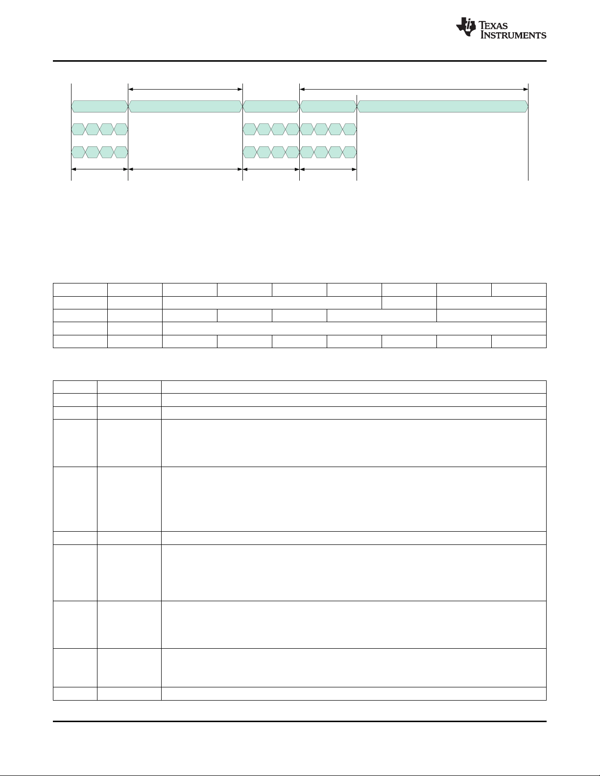
FFh 00h 00h XYh
SAV Channel Data
SC3 SC2 SC1 SC0
SAV for
encapsulated
frame
CbYCr
Y
FFh 00h 00h XYh
EAV
Start code for
channel data
EAV for
encapsulated
frame
Horizontal Active Period (SAV2EAV)
FFh 00h 00h XYhFFh 00h 00h XYh
SC3 SC2 SC1 SC0
Y Y
Cb Cr
Horizontal Blanking Interval
64 clock cycles (fixed)
EAV2SAV Start Code
TVP5158, TVP5157, TVP5156
SLES243D–JULY 2009–REVISED OCTOBER 2010
Figure 3-16. Start Code in 16-Bit YCbCr 4:2:2 Interface
Table 3-12 and Table 3-13 show the bit assignment and field definition of 4-Byte start code for Active
Video Line.
Table 3-12. Bit Assignment of 4-Byte Start Code for Active Video Line
BYTE 7 6 5 4 3 2 1 0
SC[3] 1 RSVD VCS_ID CH_ID[1:0]
SC[2] 0 BOL EOL VDET RSVD LN_ID[8:7]
SC[1] ~LD_ID[6] LN_ID[6:0]
SC[0] 1 F V H P3 P2 P1 P0
www.ti.com
Table 3-13. Bit Field Definition of 4-Byte Start Code for Active Video Line
BIT NAME FUNCTION
31 1 Always set to 1.
[30:27] RSVD Reserved
Video cascade stage ID. Set to 0 for normal operation. In cascade mode, the back-end device (e.g.,
26 VCS_ID
[25:24] CH_ID[1:0] 01: Channel 2
23 0 Always set to 0.
22 BOL
21 EOL
20 VDET 0: Video not detected
[19:18] RSVD Reserved
30 Functional Description Copyright © 2009–2010, Texas Instruments Incorporated
TMS320DM6467) interfaces to the first stage.
0: First stage (channels 1 to 4)
1: Second stage (channels 5 to 8)
2-bit Channel ID. Video decoder channel number.
00: Channel 1
10: Channel 3
11: Channel 4
Active-high beginning of line flag. Used in split-line mode which may be required for hybrid formats (e.g.
1-Ch D1 + 8-Ch CIF). Set high when the current encapsulated line of channel data includes the beginning of
a video line.
0: BOL not included (2nd half of split line)
1: BOL included (1st half of split line or full line)
Active-high end of line flag. Used in split-line mode which may be required for hybrid formats (e.g. 1-Ch D1 +
8-Ch CIF). Set high when the current line of channel data includes the end of a video line.
0: EOL not included (1st half of split line)
1: EOL included (2nd half of split line or full line)
Active-high video detection status
1: Video detected
Submit Documentation Feedback
Product Folder Link(s): TVP5158 TVP5157 TVP5156

TVP5158, TVP5157, TVP5156
www.ti.com
SLES243D–JULY 2009–REVISED OCTOBER 2010
Table 3-13. Bit Field Definition of 4-Byte Start Code for Active Video Line (continued)
BIT NAME FUNCTION
[17:16] LN_ID[8:7] video (i.e., resets once per field). During the vertical blanking interval, the line counter may either continue
15 ~LN_ID[6] Always set to the complement of bit 14 (LN_ID[6]).
[14:8] LN_ID[6:0] video (i.e., resets once per field). During the vertical blanking interval, the line counter may either continue
7 1 Always set to 1.
6 F 0: First field of frame
5 V 0: when not in vertical blanking
4 H 0: SAV
3 P3 P3 = V XOR H, Protection bits used for error detection/correction
2 P2 P2 = F XOR H, Protection bits used for error detection/correction
1 P1 P1 = F XOR V, Protection bits used for error detection/correction
0 P0 P0 = F XOR V XOR H, Protection bits used for error detection/correction
Two MSBs of 9-bit Line ID, active video line number. Line counter resets to 000h at beginning of active
counting or hold the terminal count determined at the end of active video.
Seven LSBs of 9-bit Line ID, active video line number. Line counter resets to 000h at beginning of active
counting or hold the terminal count determined at the end of active video.
F-bit
1: Second field of frame
V-bit
1: during vertical blanking
H-bit. Always set to 0.
1: EAV (never used)
NOTE
For line-interleaved output mode, if none of video decoder channels has the data ready at a
given time, TVP5158 outputs the dummy line until any one of video decoder channels is
ready to output a line. The backend chip needs to keep only the active video line and ignore
the dummy line.
The start code of the dummy line is different with active video line. Table 3-14 shows the bit assignment
and field definition of 4-Byte start code for the Dummy Line.
Table 3-14. Bit Assignment of 4-Byte Start Code for the Dummy Line
BYTE 7 6 5 4 3 2 1 0
SC[3] 0 0 0 0 0 0 0 1
SC[2] 0 0 0 0 0 0 0 1
SC[1] 0 0 0 0 0 0 0 1
SC[0] 0 0 0 0 0 0 0 1
NOTE
The Dummy Line can be distinguished from active video line by looking at the MSB of byte
SC[0].
Copyright © 2009–2010, Texas Instruments Incorporated Functional Description 31
Submit Documentation Feedback
Product Folder Link(s): TVP5158 TVP5157 TVP5156

TVP5158, TVP5157, TVP5156
SLES243D–JULY 2009–REVISED OCTOBER 2010
3.9 Audio Sub-System (TVP5157 and TVP5158 Only)
The audio sub-system integrates a 4-Ch audio analog-to-digital converter, digital processing, and I2S
encoder. TVP5158 audio sub-system supports 4-Ch mono analog audio input and standard/multiple I2S
output. TVP5158 also supports audio cascade connection up to four devices cascade connected for 16-Ch
audio input.
3.9.1 Features
• Four mono analog audio input channels
– Requires external passive attenuator to support 2.828-Vpp analog audio input
• Programmable Gain Amplifier (PGA)
– Gain range: -12 ~ 0 dB, Gain Step: 1.5 dB
• Integrated Anti-Aliasing Filter (AAF)
• 10-Bit Analog-to-Digital Converter
• Integrates Audio High-pass filter to eliminate low frequency hum
• Digital serial audio interface
– 16-Bit Linear PCM, 8-Bit A-Law and 8-Bit µ-Law Data
– I2S or DSP Format
– Master and Slave mode operation
– Up to 16 slots TDM output
– 64 fsor 256 fssystem clock
• Sampling Rate : 16 kHz, 8 kHz
• Audio Cascade connection
– Up to 4 cascaded devices
– I2S format
– 256 fssystem clock
• Audio Mixing Output
– Audio ADC has one register to set mix ratio
– The Mixing output pin SD_M can also be used for recording. Combined with the recording output
pin SD_R, two I2S bit-streams can be output simultaneously.
www.ti.com
32 Functional Description Copyright © 2009–2010, Texas Instruments Incorporated
Submit Documentation Feedback
Product Folder Link(s): TVP5158 TVP5157 TVP5156

TVP5158, TVP5157, TVP5156
www.ti.com
3.9.2 Audio Sub-System Functional Diagram
SLES243D–JULY 2009–REVISED OCTOBER 2010
Figure 3-17. Audio Sub-System Functional Diagram
3.9.3 Serial Audio Interface
The timing for the TVP5158 serial audio interface is shown in Figure 3-18. The TVP5158 audio data
output (SD_R) and frame sync pulse (LRCLK) are aligned with the falling edge of the bit clock (BCLK).
The TVP5158 audio data is delayed one BCLK cycles from the falling edge of the frame sync pulse. In the
DSP mode, the TVP5158 frame sync pulse is high for only one BCLK cycle.
Copyright © 2009–2010, Texas Instruments Incorporated Functional Description 33
Submit Documentation Feedback
Product Folder Link(s): TVP5158 TVP5157 TVP5156

LRCLK_R
BCLK_R
SD_R
(a) I
2
S Format
1/f
s
MSB MSB
LRCLK_R
BCLK_R
SD_R
(b) DSP Format
1/f
s
MSB LSB MSB
LSB
LSB
LSB
LSB
LSB
Data 1 Data 2
Data 1 Data 2
TVP5158, TVP5157, TVP5156
SLES243D–JULY 2009–REVISED OCTOBER 2010
Figure 3-18. Serial Audio Interface Timing Diagram
www.ti.com
3.9.4 Analog Audio Input Clamping
An internal clamping circuit provides mid-level clamping of all four analog audio inputs to a dc level of
approximately 0.625 V.
34 Functional Description Copyright © 2009–2010, Texas Instruments Incorporated
Product Folder Link(s): TVP5158 TVP5157 TVP5156
Submit Documentation Feedback

TVP5158
First Stage
AIN_1
AIN_2
AIN_3
AIN_4
BCL K_R
LRCL K_R
SD_ R
SD_ M
SD_CI
SD_CO
TVP5158
Second Stage
AIN_5
AIN_6
AIN_7
AIN_8
SD_CI
SD_CO
TVP5158
Third Stage
AIN_9
AIN_10
AIN_11
AIN_12
SD_CI
SD_CO
TVP5158
Last Stage
AIN_13
AIN_14
AIN_15
AIN_16
BCL K_R
LRCL K_R
SD_ R
SD_CI
SD_CO
Record Output
(AIN_ 13-AN_16 )
Record Output
(AIN_ 9-AN_16)
Record Output
(AIN_ 5-AN_16)
Record Output
(AIN_ 1-AN_16)
Mix Outpu t
BC LK_CI
LRCL K_CI
SD_ M
BC LK_R
LRCLK_R
SD _R
SD _M
BCL K_R
LRCL K_R
SD_R
BCLK_CI
SD_M
BC LK_R
LRCLK_R
SD_R
SD_M
LRC LK_CI
BCL K_R
LRCL K_R
SD_R
BCLK_CI
SD_M
BC LK_R
LRCLK_R
SD_R
SD_M
LRC LK_CI
XTAL_IN
OSC_OUT
XTAL_IN
OSC_OUT
XTAL_IN
OSC_OUT
XTAL_OUT
OSC_OUT
XTAL_IN
XTAL
TVP5158, TVP5157, TVP5156
www.ti.com
3.9.5 Audio Cascade Connection
SLES243D–JULY 2009–REVISED OCTOBER 2010
TVP5158 supports up to four devices cascaded together for audio cascade connection. The I2S output of
master TVP5158 (1st stage) combines all audio channel data from cascaded TVP5158 devices.
Key Features of Audio Cascade Connection
Figure 3-19. Audio Cascade Connection
• 16-Bit linear PCM data
s
• I2S format
• Bit Clock: 256 f
• All cascade inputs are always in slave mode
• Second to fourth stage serial audio outputs are always in master mode
• First stage serial audio output can be in either master or slave mode
• Common clock source for all cascaded devices is required
The Serial Audio Output Channel Assignment shown on Table 3-15.
Copyright © 2009–2010, Texas Instruments Incorporated Functional Description 35
Product Folder Link(s): TVP5158 TVP5157 TVP5156
Submit Documentation Feedback

TVP5158, TVP5157, TVP5156
SLES243D–JULY 2009–REVISED OCTOBER 2010
www.ti.com
Table 3-15. Serial Audio Output Channel Assignment
I2S
LRCLK_R Left LRCLK_R Right
tdm_ch tdm_out_pin Slot 1 Slot 2 Slot 3 Slot 4 Slot 5 Slot 6 Slot 7 Slot 8 Slot 9 Slot 10 Slot 11 Slot 12 Slot 13 Slot 14 Slot 15 Slot 16
SD_R AIN_1 AIN_2
0
0 (2 channel)
1 (4 channel)
2 (8 channel)
3 (12 channel)
4 (16 channel)
DSP Format
tdm_ch tdm_out_pin Slot 1 Slot 2 Slot 3 Slot 4 Slot 5 Slot 6 Slot 7 Slot 8 Slot 9 Slot 10 Slot 11 Slot 12 Slot 13 Slot 14 Slot 15 Slot 16
0 (2 channel)
1 (4 channel)
2 (8 channel)
3 (12 channel)
4 (16 channel)
SD_M
SD_R AIN_1
1
SD_M AIN_2
SD_R AIN_1 AIN_3 AIN_2 AIN_4
0
SD_M
SD_R AIN_1 AIN_2
1
SD_M AIN_3 AIN_4
SD_R AIN_1 AIN_3 AIN_5 AIN_7 AIN_2 AIN_4 AIN_6 AIN_8
0
SD_M
SD_R AIN_1 AIN_5 AIN_2 AIN_6
1
SD_M AIN_3 AIN_7 AIN_4 AIN_8
SD_R AIN_1 AIN_3 AIN_5 AIN_7 AIN_9 AIN_11 AIN_2 AIN_4 AIN_6 AIN_8 AIN_10 AIN_12
0
SD_M
SD_R AIN_1 AIN_5 AIN_9 AIN_2 AIN_6 AIN_10
1
SD_M AIN_3 AIN_7 AIN_11 AIN_4 AIN_8 AIN_12
SD_R AIN_1 AIN_3 AIN_5 AIN_7 AIN_9 AIN_11 AIN_13 AIN_15 AIN_2 AIN_4 AIN_6 AIN_8 AIN_10 AIN_12 AIN_14 AIN_16
0
SD_M
SD_R AIN_1 AIN_5 AIN_9 AIN_13 AIN_2 AIN_6 AIN_10 AIN_14
1
SD_M AIN_3 AIN_7 AIN_11 AIN_15 AIN_4 AIN_8 AIN_12 AIN_16
SD_R AIN_1 AIN_2
0
SD_M
SD_R AIN_1
1
SD_M AIN_2
SD_R AIN_1 AIN_3 AIN_2 AIN_4
0
SD_M
SD_R AIN_1 AIN_2
1
SD_M AIN_3 AIN_4
SD_R AIN_1 AIN_3 AIN_5 AIN_7 AIN_2 AIN_4 AIN_6 AIN_8
0
SD_M
SD_R AIN_1 AIN_5 AIN_2 AIN_6
1
SD_M AIN_3 AIN_7 AIN_4 AIN_8
SD_R AIN_1 AIN_3 AIN_5 AIN_7 AIN_9 AIN_11 AIN_2 AIN_4 AIN_6 AIN_8 AIN_10 AIN_12
0
SD_M
SD_R AIN_1 AIN_5 AIN_9 AIN_2 AIN_6 AIN_10
1
SD_M AIN_3 AIN_7 AIN_11 AIN_4 AIN_8 AIN_12
SD_R AIN_1 AIN_3 AIN_5 AIN_7 AIN_9 AIN_11 AIN_13 AIN_15 AIN_2 AIN_4 AIN_6 AIN_8 AIN_10 AIN_12 AIN_14 AIN_16
0
SD_M
SD_R AIN_1 AIN_5 AIN_9 AIN_13 AIN_2 AIN_6 AIN_10 AIN_14
1
SD_M AIN_3 AIN_7 AIN_11 AIN_15 AIN_4 AIN_8 AIN_12 AIN_16
3.10 I2C Host Interface
The I2C standard consists of two signals, serial input/output data line (SDA) and input/output clock line
(SCL), which carry information between the devices connected to the bus. The input pins I2CA0, I2CA1
and I2CA2 are used to select the slave address to which the device responds. Although the I2C system
can be multi-mastered, the TVP5158 decoder functions as a slave device only.
36 Functional Description Copyright © 2009–2010, Texas Instruments Incorporated
Submit Documentation Feedback
Product Folder Link(s): TVP5158 TVP5157 TVP5156

TVP5158, TVP5157, TVP5156
www.ti.com
SLES243D–JULY 2009–REVISED OCTOBER 2010
Both SDA and SCL must be connected to IOVDD via pullup resistors. When the bus is free, both lines are
high. The slave address select terminals (I2CA0, I2CA1 and I2CA2) enable the use of up to eight devices
on the same I2C bus. At the trailing edge of reset, the status of the I2CA0, I2CA1 and I2CA2 lines are
sampled to determine the device address used. Table 3-16 summarizes the terminal functions of the I2C
host interface. Table 3-17 shows the device address selection options.
Table 3-16. I2C Terminal Description
SIGNAL TYPE DESCRIPTION
I2CA0 I Slave address selection
I2CA1 I Slave address selection
I2CA2 I Slave address selection
SCL I/O (open drain) Input/output clock line
SDA I/O (open drain) Input/output data line
Table 3-17. I2C Host Interface Device Addresses
A6 A5 A4 A3 A2(I2CA2) A1(I2CA1) A0 (I2CA0) R/W HEX
1 0 1 1 0 0 0 1/0 B1/B0
1 0 1 1 0 0 1 1/0 B3/B2
1 0 1 1 0 1 0 1/0 B5/B4
1 0 1 1 0 1 1 1/0 B7/B6
1 0 1 1 1 0 0 1/0 B9/B8
1 0 1 1 1 0 1 1/0 BB/BA
1 0 1 1 1 1 0 1/0 BD/BC
1 0 1 1 1 1 1 1/0 BF/BE
Data transfer rate on the bus is up to 400 kbit/s. The number of devices connected to the bus is
dependent on the bus capacitance limit of 400 pF. The data on the SDA line must be stable during the
high period of the SCL except for start and stop conditions. The high or low state of the data line can only
change with the clock signal on the SCL line being low. A high-to-low transition on the SDA line while the
SCL is high indicates an I2C start condition. A low-to-high transition on the SDA line while the SCL is high
indicates an I2C stop condition.
Every byte placed on the SDA must be 8 bits long. The number of bytes which can be transferred is
unrestricted. Each byte must be followed by an acknowledge bit. The acknowledge-related clock pulse is
generated by the I2C master.
To simplify programming of each of the 4 decoder channels a single I2C write transaction can be
transmitted to any one or more of the 4 cores in parallel. This reduces the time required to download
firmware or to configure the device when all channels are to be configured in the same manner. It also
enables the addresses for all registers to be common across all decoders.
I2C sub-address FEh contains 4 bits with each bit corresponding to one of the decoder cores. If a decoder
write enable bit is set, then I2C write transactions will be sent to the corresponding decoder core. For
multi-byte I2C write transactions there are options to auto-increment the sub-address or to auto-increment
through the selected decoders or both.
I2C sub-address FFh contains 4 bits with each bit corresponding to one of the decoder cores. If a decoder
read enable bit is set, then I2C read transactions will be sent to the corresponding decoder core.
If more than one decoder is enabled for reads then the lowest numbered decoder that is enabled will
respond to the read transaction. For multi-byte I2C read transactions there are options to auto-increment
the sub-address or to auto-increment through the selected decoders or both.
Copyright © 2009–2010, Texas Instruments Incorporated Functional Description 37
Submit Documentation Feedback
Product Folder Link(s): TVP5158 TVP5157 TVP5156

TVP5158, TVP5157, TVP5156
SLES243D–JULY 2009–REVISED OCTOBER 2010
3.10.1 I2C Write Operation
Data transfers occur utilizing the following formats.
An I2C master initiates a write operation to the decoder by generating a start condition (S) followed by the
decoder I2C address (as shown below), in MSB first bit order, followed by a 0 to indicate a write cycle.
After receiving an acknowledge from the decoder, the master presents the sub-address of the register, or
the first of a block of registers it wants to write, followed by one or more bytes of data, MSB first. The
decoder acknowledges each byte after completion of each transfer. The I2C master terminates the write
operation by generating a stop condition (P).
Step 1 0
I2C Start (master) S
Step 2 7 6 5 4 3 2 1 0
I2C General address (master) 1 0 1 1 1 0 X 0
Step 3 9
I2C Acknowledge (slave) A
Step 4 7 6 5 4 3 2 1 0
I2C Write register address (master) Addr Addr Addr Addr Addr Addr Addr Addr
Step 5 9
I2C Acknowledge (slave) A
(1)
Step 6
I2C Write data (master) Data Data Data Data Data Data Data Data
(1)
Step 7
I2C Acknowledge (slave) A
www.ti.com
7 6 5 4 3 2 1 0
9
Step 8 0
I2C Stop (master) P
(1) Repeat steps 6 and 7 until all data have been written.
3.10.2 I2C Read Operation
The read operation consists of two phases. The first phase is the address phase. In this phase, an I2C
master initiates a write operation to the decoder by generating a start condition (S) followed by the
decoder slave address, in MSB first bit order, followed by a 0 to indicate a write cycle. After receiving
acknowledge from the decoder, the master presents the sub-address of the register or the first of a block
of registers it wants to read. After the cycle is acknowledged, the master has the option of generating a
stop condition or not.
In the data phase, an I2C master initiates a read operation to the decoder by generating a start condition
followed by the decoder I2C slave address (as shown below for a read operation), in MSB first bit order,
followed by a 1 to indicate a read cycle. After an acknowledge from the decoder, the I2C master receives
one or more bytes of data from the decoder. The I2C master acknowledges the transfer at the end of each
byte. After the last data byte has been transferred from the decoder, the master generates a not
acknowledge followed by a stop.
38 Functional Description Copyright © 2009–2010, Texas Instruments Incorporated
Submit Documentation Feedback
Product Folder Link(s): TVP5158 TVP5157 TVP5156

TVP5158, TVP5157, TVP5156
www.ti.com
Read Phase 1
Step 1 0
I2C Start (master) S
Step 2 7 6 5 4 3 2 1 0
I2C General address (master) 1 0 1 1 X X X 0
Step 3 9
I2C Acknowledge (slave) A
Step 4 7 6 5 4 3 2 1 0
I2C Read register address (master) Addr Addr Addr Addr Addr Addr Addr Addr
Step 5 9
I2C Acknowledge (slave) A
Step 6
I2C Stop (master) P
(1) Step 6 is optional.
Read Phase 2
Step 7 0
I2C Start (master) S
Step 8 7 6 5 4 3 2 1 0
I2C General address (master) 1 0 1 1 X X X 1
SLES243D–JULY 2009–REVISED OCTOBER 2010
(1)
0
Step 9 9
I2C Acknowledge (slave) A
(1)
Step 10
7 6 5 4 3 2 1 0
I2C Read data (slave) Data Data Data Data Data Data Data Data
(1)
Step 11
9
I2C Not Acknowledge (master) A
Step 12 0
I2C Stop (master) P
(1) Repeat steps 10 and 11 for all bytes read. Master does not acknowledge the last read data received.
Copyright © 2009–2010, Texas Instruments Incorporated Functional Description 39
Submit Documentation Feedback
Product Folder Link(s): TVP5158 TVP5157 TVP5156

I2C Registers
VBUS Registers
00h
FFh
00 0000h
A0 3FFFh
VBUS
Data
VBUS
Address
VBUS [23:0]
Host
Processor
I2C
40 3EEFh
E0h
E8h
Comb
Filter RAM
E1h
EAh
40 3E50h
TVP5158, TVP5157, TVP5156
SLES243D–JULY 2009–REVISED OCTOBER 2010
3.10.3 VBUS Access
The TVP5158 video decoder has additional internal registers accessible through an indirect access to an
internal 24-bit address wide VBUS. Figure 3-20 shows the VBUS registers access.
www.ti.com
Figure 3-20. VBUS Access
VBUS Write
Single Byte
S B8 ACK E8 ACK VA0 ACK VA1 ACK VA2 ACK P
S B8 ACK E0 ACK Send Data ACK P
Multiple Bytes
S B8 ACK E8 ACK VA0 ACK VA1 ACK VA2 ACK P
S B8 ACK E1 ACK Send Data ACK . . . Send Data ACK P
VBUS Read
Single Byte
S B8 ACK E8 ACK VA0 ACK VA1 ACK VA2 ACK P
S B8 ACK E0 ACK S B9 ACK Read Data NAK P
Multiple Bytes
S B8 ACK E8 ACK VA0 ACK VA1 ACK VA2 ACK P
S B8 ACK E1 ACK S B9 ACK Read Data MACK . . . Read Data NAK P
NOTE: Examples use default I2C address
ACK: Acknowledge generated by the slave
MACK: Acknowledge generated by the master
NAK: No Acknowledge generated by the master
40 Functional Description Copyright © 2009–2010, Texas Instruments Incorporated
Submit Documentation Feedback
Product Folder Link(s): TVP5158 TVP5157 TVP5156

VSSA
27-MHz
Crystal
27-MHz CLK
Output to other TVP5158
XTAL_IN pin
27-MHz CLK
Output to other TVP5158
XTAL_IN pin
0 W
TVP5158, TVP5157, TVP5156
www.ti.com
3.11 Clock Circuits
An analog clock multiplier PLL is used to generate a system clock from an external 27-MHz crystal
(fundamental resonant frequency) or external clock reference input. A crystal can be connected across
terminals 99 (XTAL_IN) and 101 (XTAL_OUT), or a 1.8-V external clock input can be connected to
terminal 99. Four horizontal PLLs generate the line-locked sample clock for each video decoder core from
the system clock. Four color PLLs generate the color subcarrier frequency for each video decoder core
from the corresponding line-locked clock. Four vertical PLLs generate the field/frame sync for each video
decoder core. A frequency synthesizer generates the 32.768-MHz audio oversampling clock for each
analog audio input from the system clock.
Figure 3-21 shows the reference clock configurations. For the example crystal circuit shown, the external
capacitors must have the following relationship:
CL1= CL2= 2CL– C
Where C
specified by the crystal manufacturer.
is the terminal capacitance with respect to ground, and CLis the crystal load capacitance
STRAY
SLES243D–JULY 2009–REVISED OCTOBER 2010
STRAY
Figure 3-21. Clock and Crystal Connectivity
Copyright © 2009–2010, Texas Instruments Incorporated Functional Description 41
Submit Documentation Feedback
Product Folder Link(s): TVP5158 TVP5157 TVP5156

RESETB
(Terminal 3)
Reset
Normal operation
Invalid I C Cycle
2
Valid
260 µs (min)
20 ms (min)
TVP5158, TVP5157, TVP5156
SLES243D–JULY 2009–REVISED OCTOBER 2010
3.12 Reset Mode
Terminals 3 (RESETB) is active low signal to hold the decoder into reset. Table 3-18 shows the
configuration of reset mode. Table 3-19 describes the status of the decoder signals during and
immediately after reset. Figure 3-22 shows the reset timing.
After power-up, the device will be in an unknown state until properly reset. An active low reset, Reset B, of
greater than or equal to 20 ms is required following active and stable supply ramp-up. To avoid potential
I2C issues, keep SCL and SDA inactive (high) for at least 260 µs after reset goes high. There are no
power sequencing requirements except that all power supplies should become active and stable within
500 ms of each other.
Table 3-18. Reset Mode
RESETB CONFIGURATION
0 Resets the decoder
1 Normal operation
Table 3-19. Reset Sequence
SIGNAL NAME DURING RESET RESET COMPLETED
DVO_A_[7:0], DVO_B_[7:0], DVO_C_[7:0], DVO_D_[7:0], OCLK_P, OCLK_N,
INTREQ, I2CA[2:0], BCLK_R, LRCLK_R, SD_R, SD_M, SD_CO
RESETB, SDA, SCL, LRCLK_CI, BCLK_CI, SD_CI, XTAL_IN Input Input
XTAL_OUT, OSC_OUT Output Output
www.ti.com
Input High-impedance
Figure 3-22. Reset Timing
42 Functional Description Copyright © 2009–2010, Texas Instruments Incorporated
Submit Documentation Feedback
Product Folder Link(s): TVP5158 TVP5157 TVP5156

TVP5158, TVP5157, TVP5156
www.ti.com
SLES243D–JULY 2009–REVISED OCTOBER 2010
4 Internal Control Registers
4.1 Overview
The decoder is initialized and controlled by a set of internal registers which set all device operating
parameters. Communication between the external controller and the decoder is through I2C. Table 4-1
shows the summary of these registers. The reserved registers must not be written. Reserved bits in the
defined registers must be written with 0s, unless otherwise noted. The detailed programming information
of each register is described in the following sections.
I2C register FEh controls which of the four decoders will receive I2C commands. I2C register FFh controls
which decoder core responds to I2C reads. Note, for a read operation it is necessary to perform a write
first in order to set the desired sub-address for reading.
Compared to previous video decoder, TVP5154A, the TVP5156, TVP5157, and TVP5158 add decoder
auto increment and address auto increment bits control. If decoder auto increment bit is set, the next
read/write is from/to the next decoder that is enabled. If address auto increment bit is set, the address will
increment after all the decoders enabled read/writes are completed. The detail of I2C registers FEh and
FFh is shown in their register section.
Table 4-1. Registers Summary
REGISTER NAME I2C SUBADDRESS DEFAULT R/W
Status 1 00h R
Status 2 01h R
Color Subcarrier Phase Status 02h R
Reserved 03h
ROM Version 04h R
Reserved 05h - 07h
Chip ID MSB 08h 51h R
Chip ID LSB 09h 58h R
Reserved 0Ah - 0Bh
Video Standard Status 0Ch R
Video Standard Select 0Dh 00h R/W
CVBS Autoswitch Mask 0Eh 03h R/W
Auto Contrast Mode 0Fh 03h R/W
Luminance Brightness 10h 80h R/W
Luminance Contrast 11h 80h R/W
Brightness and Contrast Range Extender 12h 00h R/W
Chrominance Saturation 13h 80h R/W
Chrominance Hue 14h 00h R/W
Reserved 15h
Color Killer 16h 10h R/W
Reserved 17h
Luminance Processing Control 1 18h 40h R/W
Luminance Processing Control 2 19h 00h R/W
Power Control 1Ah 00h R/W
Chrominance Processing Control 1 1Bh 00h R/W
Chrominance Processing Control 2 1Ch 0Ch R/W
Reserved 1Dh - 1Fh
AGC Gain Status 1 20h R
AGC Gain Status 2 21h R
(1)
(1) R = Read only, W = Write only, R/W = Read and write
Copyright © 2009–2010, Texas Instruments Incorporated Internal Control Registers 43
Submit Documentation Feedback
Product Folder Link(s): TVP5158 TVP5157 TVP5156

TVP5158, TVP5157, TVP5156
SLES243D–JULY 2009–REVISED OCTOBER 2010
Table 4-1. Registers Summary (continued)
REGISTER NAME I2C SUBADDRESS DEFAULT R/W
Reserved 22h
Back-End AGC Status 23h R
Status Request 24h 00h R/W
AFE Gain Control 25h F5h R/W
Luma ALC Freeze Upper Threshold 26h 00h R/W
Chroma ALC Freeze Upper Threshold 27h 00h R/W
Reserved 28h
AGC Increment Speed 29h 06h R/W
AGC Increment Delay 2Ah 1Eh R/W
AGC Decrement Speed 2Bh 04h R/W
AGC Decrement Delay 2Ch 00h R/W
AGC White Peak Processing 2Dh F2h R/W
Back-End AGC Control 2Eh 08h R/W
Reserved 2Fh - 33h
AFE Fine Gain 34h - 35h 086Ah R/W
Reserved 36h - 47h
AVID Start Pixel LSBs 48h 7Ah/84h R/W
AVID Start Pixel MSBs 49h 00h/00h R/W
AVID Pixel Width 4Ah - 4Bh 02D0h/02D0h R/W
Reserved 4Ch - 5Bh
NR_Max_Noise 5Ch 28h R/W
NR_Control 5Dh 09h R/W
NR_Noise_Filter 5Eh - 5Fh 0330h R/W
Operation Mode Control 60h 00h R/W
Color PLL Speed Control 61h 09h R/W
Reserved 62h - 7Bh
Sync Height Low Threshold 7Ch 02h R/W
Sync Height High Threshold 7Dh 08h R/W
Reserved 7Eh - 80h 03h R/W
Clear Lost Lock Detect 81h 00h R/W
Reserved 82h - 84h
V-Sync Filter Shift 85h 03h R/W
Reserved 86h
656 Version/F Bit Control 87h 00h R/W
F- and V-Bit Decode Control 88h 00h R/W
F- and V-Bit Control 89h 16h R/W
Reserved 8Ah - 8Bh
Output Timing Delay 8Ch 00h R/W
Reserved 8Dh - 8Fh
Auto Contrast User Table Index 8Fh 04h R/W
Blue Screen Y Control 90h 10h R/W
Blue Screen Cb Control 91h 80h R/W
Blue Screen Cr Control 92h 80h R/W
Blue Screen LSB Control 93h 00h R/W
Noise Measurement LSB 94h R
Noise Measurement MSB 95h R
Weak Signal High Threshold 96h 60h R/W
www.ti.com
(1)
44 Internal Control Registers Copyright © 2009–2010, Texas Instruments Incorporated
Submit Documentation Feedback
Product Folder Link(s): TVP5158 TVP5157 TVP5156

TVP5158, TVP5157, TVP5156
www.ti.com
SLES243D–JULY 2009–REVISED OCTOBER 2010
Table 4-1. Registers Summary (continued)
REGISTER NAME I2C SUBADDRESS DEFAULT R/W
Weak Signal Low Threshold 97h 50h R/W
Reserved 98h - 9Dh
NR_Y_T0 9Eh 0Ah R/W
NR_U_T0 9Fh BCh R/W
NR_V_T0 A0h BCh R/W
Reserved A1h
Vertical Line Count Status A2h - A3h R
Reserved A4h - A7H
Output Formatter Control 1 (write to all four decoder cores) A8h 44h R/W
Output Formatter Control 2 (write to all four decoder cores) A9h 40h R/W
Reserved AAh - ACh
Interrupt Control ADh 00h R/W
Embedded Sync Offset Control 1 (write to all four decoder cores) AEh 00h R/W
Embedded Sync Offset Control 2 (write to all four decoder cores) AFh 00h R/W
AVD Output Control 1 B0h 00h R/W
AVD Output Control 2 B1h 10h R/W
OFM Mode Control B2h 20h R/W
OFM Channel Select 1 B3h E4h R/W
OFM Channel Select 2 B4h E4h R/W
OFM Channel Select 3 B5h 00h R/W
OFM Super-Frame Size LSBs B6h 1Bh R/W
OFM Super-Frame Size MSBs B7h 04h R/W
OFM H-Blank Duration LSBs B8h 40h R/W
OFM H-Blank Duration MSBs B9h 00h R/W
Misc Ofm Control BAh 00h R/W
Reserved BBh - BFh 00h R/W
Audio Sample Rate Control C0h 00h R/W
Analog Audio Gain Control 1 C1h 88h R/W
Analog Audio Gain Control 2 C2h 88h R/W
Audio Mode Control C3h C9h R/W
Audio Mixer Select C4h 01h R/W
Audio Mute Control C5h 00h R/W
Audio Mixing Ratio Control 1 C6h 00h R/W
Audio Mixing Ratio Control 2 C7h 00h R/W
Audio Cascade Mode Control C8h 00h R/W
Reserved C9h A5h R/W
Reserved CAh FFh R/W
Reserved CBh 7Eh R/W
Reserved CCh 01h R/W
Reserved CDh - CFh
Super-frame EAV2SAV duration status LSBs D0h R
Super-frame EAV2SAV duration status MSBs D1h R
Super-frame SAV2EAV duration status LSBs D2h R
Super-frame SAV2EAV duration status MSBs D3h R
Reserved D4h - DFh
VBUS Data Access With No VBUS Address Increment E0h R/W
VBUS Data Access With VBUS Address Increment E1h R/W
(1)
Copyright © 2009–2010, Texas Instruments Incorporated Internal Control Registers 45
Submit Documentation Feedback
Product Folder Link(s): TVP5158 TVP5157 TVP5156

TVP5158, TVP5157, TVP5156
SLES243D–JULY 2009–REVISED OCTOBER 2010
www.ti.com
Table 4-1. Registers Summary (continued)
REGISTER NAME I2C SUBADDRESS DEFAULT R/W
Reserved E2h - E7h
VBUS Address Access E8h - EAh 00 0000h R/W
Reserved EBh - F1h R/W
Interrupt Status F2h R
Reserved F3h
Interrupt Mask F4h 00h R/W
Reserved F5h
Interrupt Clear F6h 00h R/W
Decoder Write Enable FEh 0Fh R/W
Decoder Read Enable FFh 01h R/W
4.2 Register Definitions
Table 4-2. Status 1
Subaddress 00h
Default Read only
7 6 5 4 3 2 1 0
Reserved Lost lock detect subcarrier lock TV/VCR status
Line-alternating status
0 Non line alternating
1 Line alternating
Field rate status
0 60 Hz
1 50 Hz
Lost lock detect
0 No lost lock since this bit was last cleared
1 Lost lock since this bit was last cleared
Color subcarrier lock status
0 Color subcarrier is not locked
1 Color subcarrier is locked
Vertical sync lock status
0 Vertical sync is not locked
1 Vertical sync is locked
Horizontal sync lock status
0 Horizontal sync is not locked
1 Horizontal sync is locked
TV/VCR status
0 TV
1 VCR
Line-alternating Field rate Vertical sync Horizontal sync
status status lock status lock status
Color
status
(1)
46 Internal Control Registers Copyright © 2009–2010, Texas Instruments Incorporated
Submit Documentation Feedback
Product Folder Link(s): TVP5158 TVP5157 TVP5156

TVP5158, TVP5157, TVP5156
www.ti.com
SLES243D–JULY 2009–REVISED OCTOBER 2010
Table 4-3. Status 2
Subaddress 01h
Default Read only
7 6 5 4 3 2 1 0
Signal present Color killed Macrovision detection [2:0]
Signal present
0 Signal is not present
1 Signal is present
Weak signal detection
0 No weak signal
1 Weak signal mode
PAL switch polarity
0 PAL switch is zero
1 PAL switch is one
Field sequence status
0 Even field
1 Odd field
Color killed
0 Color killer is not active
1 Color killer is active
Macrovision detection [2:0]
000 No copy protection
001 AGC pulses/pseudo syncs present (Type 1)
010 2-line colorstripe only present
011 AGC pulses/pseudo syncs and 2-line colorstripe present (Type 2)
100 Reserved
101 Reserved
110 4-line colorstripe only present
111 AGC pulses/pseudo syncs and 4-line colorstripe present (Type 3)
Weak signal PAL switch Field sequence
detection polarity status
Table 4-4. Color Subcarrier Phase Status
Subaddress 02h
Default Read only
7 6 5 4 3 2 1 0
Color subcarrier phase [7:0]
This register shows the color subcarrier phase.
Table 4-5. ROM Version
Subaddress 04h
Default Read only
7 6 5 4 3 2 1 0
ROM version [7:0]
ROM Version [7:0]
ROM revision number = 02h for PG 1.1
Copyright © 2009–2010, Texas Instruments Incorporated Internal Control Registers 47
Submit Documentation Feedback
Product Folder Link(s): TVP5158 TVP5157 TVP5156

TVP5158, TVP5157, TVP5156
SLES243D–JULY 2009–REVISED OCTOBER 2010
Table 4-6. Chip ID MSB
Subaddress 08h
Default Read only
7 6 5 4 3 2 1 0
Chip ID MSB [7:0]
Chip ID MSB[7:0]
This register identifies the MSB of device ID. Value = 51h
Table 4-7. Chip ID LSB
Subaddress 09h
Default Read only
7 6 5 4 3 2 1 0
Chip ID LSB [7:0]
Chip ID LSB [7:0]
This register identifies the LSB of device ID. Value = 58h
Table 4-8. Video Standard Status
www.ti.com
Subaddress 0Ch
Default Read only
7 6 5 4 3 2 1 0
Autoswitch Reserved Video standard [2:0]
This register contains information about the detected video standard that the device is currently operating. When in autoswitch mode, this
register can be tested to determine which video standard as has been detected. See subaddress: 0Dh.
Autoswitch Mode
0 Single standard set
1 Autoswitch mode enabled
Video Standard [2:0]
00h Reserved
01h (M, J) NTSC
02h (B, D, G, H, I, N) PAL
03h (M) PAL
04h (Combination-N) PAL
05h NTSC 4.43
06h Reserved
07h PAL 60
48 Internal Control Registers Copyright © 2009–2010, Texas Instruments Incorporated
Submit Documentation Feedback
Product Folder Link(s): TVP5158 TVP5157 TVP5156

TVP5158, TVP5157, TVP5156
www.ti.com
SLES243D–JULY 2009–REVISED OCTOBER 2010
Table 4-9. Video Standard Select
Subaddress 0Dh
Default 00h
7 6 5 4 3 2 1 0
Reserved CVBS Standard [2:0]
The user can force the device to operate in a particular video standard mode by writing the appropriate value into this register. Changing
these bits will cause some register settings to be reset to their defaults. See subaddress: 0Ch.
CVBS Standard [2:0]
00h CVBS Autoswitch mode (default)
01h (M, J) NTSC
02h (B, D, G, H, I, N) PAL
03h (M) PAL
04h (Combination-N) PAL
05h NTSC 4.43
06h Reserved
07h PAL 60
Table 4-10. CVBS Autoswitch Mask
Subaddress 0Eh
Default 03h
7 6 5 4 3 2 1 0
Reserved PAL 60 Reserved NTSC 4.43 (Nc) PAL (M) PAL PAL (M, J) NTSC
Autoswitch mode mask
Limits the video formats between which autoswitch is possible.
PAL 60 0 Autoswitch does not include PAL 60 (default)
1 Autoswitch includes PAL 60
NTSC 4.43 0 Autoswitch does not include NTSC 4.43 (default)
1 Autoswitch includes NTSC 4.43
(Nc) PAL 0 Autoswitch does not include (Nc) PAL (default)
1 Autoswitch includes (Nc) PAL
(M) PAL 0 Autoswitch does not include (M) PAL (default)
1 Autoswitch includes (M) PAL
PAL 0 Reserved
1 Autoswitch includes (B, D, G, H, I, N) PAL (default)
(M, J) NTSC 0 Reserved
1 Autoswitch includes (M, J) NTSC (default)
Table 4-11. Auto Contrast Mode
Subaddress 0Fh
Default 03h
7 6 5 4 3 2 1 0
Reserved Auto Contrast Mode [1:0]
Auto Contrast Mode [1:0]
00h Enabled
01h Reserved
02h User Mode
03h Disabled (default)
Copyright © 2009–2010, Texas Instruments Incorporated Internal Control Registers 49
Submit Documentation Feedback
Product Folder Link(s): TVP5158 TVP5157 TVP5156

TVP5158, TVP5157, TVP5156
SLES243D–JULY 2009–REVISED OCTOBER 2010
Table 4-12. Luminance Brightness
Subaddress 10h
Default 80h
7 6 5 4 3 2 1 0
Brightness [7:0]
Brightness [7:0]
This register works for the luminance. See subaddress 12h.
0000 0000 0 (dark)
1000 0000 128 (default)
1111 1111 255 (bright)
The output black level relative to the nominal black level (64 out of 1024) as a function of the Brightness[7:0] setting is as follows:
Black Level = nominal_black_level + (MB+ 1) × (Brightness[7:0] - 128)
Where MBis the brightness multiplier setting in the Brightness and Contrast Range Extender register at I2C subaddress 12h.
Table 4-13. Luminance Contrast
Subaddress 11h
Default 80h
7 6 5 4 3 2 1 0
Contrast [7:0]
Contrast [7:0]
This register works for the luminance. See subaddress 12h.
0000 0000 0 (minimum contrast)
1000 0000 128 (default)
1111 1111 255 (maximum contrast)
The total luminance gain relative to the nominal luminance gain as a function of the Contrast [7:0] setting is as follows:
Luminance Gain = (nominal_luminance_gain) × [Contrast[7:0] / 64 / (2MC) + MC- 1]
Where MCis the contrast multiplier setting in the Brightness and Contrast Range Extender register at I2C subaddress 12h.
www.ti.com
Table 4-14. Brightness and Contrast Range Extender
Subaddress 12h
Default 00h
7 6 5 4 3 2 1 0
Reserved Brightness multiplier [3:0]
Contrast multiplier [4] (MC)
Increases the contrast control range.
0 2x contrast control range (default), Gain = n/64 – 1 where n is the contrast control and 64 ≤ n ≤255
1 Normal contrast control range, Gain = n/128 where n is the contrast control and 0 ≤ n ≤ 255
Brightness multiplier [3:0] (MB)
Increases the brightness control range from 1x to 16x.
0h 1x (default)
1h 2x
3h 4x
7h 8x
Fh 16x
Note: The brightness multiplier should be set to 3h for 8-bit outputs.
50 Internal Control Registers Copyright © 2009–2010, Texas Instruments Incorporated
Product Folder Link(s): TVP5158 TVP5157 TVP5156
Contrast
multiplier
Submit Documentation Feedback

TVP5158, TVP5157, TVP5156
www.ti.com
SLES243D–JULY 2009–REVISED OCTOBER 2010
Table 4-15. Chrominance Saturation
Subaddress 13h
Default 80h
7 6 5 4 3 2 1 0
Saturation [7:0]
Saturation [7:0]
This register works for the chrominance.
0000 0000 0 (no color)
1000 0000 128 (default)
1111 1111 255 (maximum)
The total chrominance gain relative to the nominal chrominance gain as a function of the Saturation [7:0] setting is as follows:
Chrominance Gain = (nominal_chrominance_gain) × (Saturation[7:0] / 128)
Table 4-16. Chrominance Hue
Subaddress 14h
Default 80h
7 6 5 4 3 2 1 0
Hue [7:0]
Saturation [7:0]
This register works for the chrominance.
0000 0000 -180°
1000 0000 0° (default)
1111 1111 +180°
Table 4-17. Color Killer
Subaddress 16h
Default 10h
7 6 5 4 3 2 1 0
Reserved Automatic color killer Color killer threshold [4:0]
Automatic color killer
00 Automatic mode (default)
01 Reserved
10
11 Color killer disabled
Color killer threshold [4:0]:
Controls the upper and lower color killer hysteresis thresholds.
0 0000 1.0% 1.4% 0.8% 1.2%
0 1000 3.0% 4.3% 2.4% 3.5%
1 0000 5.0% 7.2% 4.0% 5.8%
1 1000 7.0% 10.0% 5.6% 8.0%
1 1111 8.8% 12.6% 7.0% 10.0%
(1) Expressed as a percent of the nominal color burst amplitude (measured after front-end AGC).
(2) For proper color killer operation, the color PLL must be locked to the color burst frequency.
Color killer enabled, The UV terminals are forced to a zero
color state.
NTSC-M,J
Lower Threshold Upper Threshold Lower Threshold Upper Threshold
(1)(2)
PAL-B,D,G,H,I,M,N
(1)(2)
Copyright © 2009–2010, Texas Instruments Incorporated Internal Control Registers 51
Submit Documentation Feedback
Product Folder Link(s): TVP5158 TVP5157 TVP5156

TVP5158, TVP5157, TVP5156
SLES243D–JULY 2009–REVISED OCTOBER 2010
Table 4-18. Luminance Processing Control 1
Subaddress 18h
Default 40h
7 6 5 4 3 2 1 0
NTSC_Ped Reserved Luminance signal delay [2:0]
NTSC_Ped
Specifies whether NTSC composite video inputs are compliant with NTSC-M or NTSC-J.
0 NTSC-M (714/286 ratio, w/ pedestal) - default
1 NTSC-J (714/286 ratio, w/o pedestal)
Luminance signal delay [2:0]
Luminance signal delays respect to chroma signal in 1x pixel clock increments.
011 3 pixel clocks delay
010 2 pixel clocks delay
001 1 pixel clocks delay
000 0 pixel clocks delay (default)
111 -1 pixel clocks delay
110 -2 pixel clocks delay
101 -3 pixel clocks delay
100 0 pixel clocks delay
Table 4-19. Luminance Processing Control 2
www.ti.com
Subaddress 19h
Default 00h
7 6 5 4 3 2 1 0
Luma filter select [1:0] Reserved Peaking gain [1:0] Trap filter select [1:0]
Luma filter selected [1:0]
00 Luminance adaptive comb enable (default)
01 Luminance adaptive comb disable (trap filter selected)
10 Luma comb/trap filter bypassed
11 Reserved
Peaking gain [1:0]
00 0 (default)
01 0.5
10 1
11 2
Trap filter select [1:0]
Selects one of the four trap filters to produce the luminance signal by removing the chrominance signal from the composite video
signal. The stop band of the chroma trap filter is centered at the chroma subcarrier frequency with the stop-band bandwidth
controlled by the two control bits.
Trap filter stop-band bandwidth (MHz)
Filter select [1:0] NTSC ITU-R BT.601 PAL ITU-R BT.601
00 = (default) 1.2129 1.2129
01 0.8701 0.8701
10 0.7183 0.7383
11 0.5010 0.5010
52 Internal Control Registers Copyright © 2009–2010, Texas Instruments Incorporated
Submit Documentation Feedback
Product Folder Link(s): TVP5158 TVP5157 TVP5156

TVP5158, TVP5157, TVP5156
www.ti.com
SLES243D–JULY 2009–REVISED OCTOBER 2010
Table 4-20. Power Control
Subaddress 1Ah
Default 00h
7 6 5 4 3 2 1 0
Pwd_ach4 Pwd_ach3 Pwd_ach2 Pwd_ach1 Pwd_vpll Pwd_ref Pwd_ofm_clk Pwd_video
Pwd_ach4
Power down audio channel 4, active high
0 Normal operation (default)
1 Audio channel 4 power down
Pwd_ach3
Power down audio channel 3, active high
0 Normal operation (default)
1 Audio channel 3 power down
Pwd_ach2
Power down audio channel 2, active high
0 Normal operation (default)
1 Audio channel 2 power down
Pwd_ach1
Power down audio channel 1, active high
0 Normal operation (default)
1 Audio channel 1 power down
Pwd_vpll
Power down video PLL, active high
0 Normal operation (default)
1 Video PLL power down
Pwd_ref
Power down bandgap reference, active high
0 Normal operation (default)
1 Bandgap reference power down
Pwd_ofm_clk
Power down OFM clock, active high
0 Normal operation (default)
1 OFM clock power down
Pwd_video
Power down video channel corresponding to current decoder core, active high
0 Normal operation (default)
1 Power down video channel corresponding to current decoder core
Copyright © 2009–2010, Texas Instruments Incorporated Internal Control Registers 53
Submit Documentation Feedback
Product Folder Link(s): TVP5158 TVP5157 TVP5156

TVP5158, TVP5157, TVP5156
SLES243D–JULY 2009–REVISED OCTOBER 2010
Table 4-21. Chrominance Processing Control 1
Subaddress 1Bh
Default 00h
7 6 5 4 3 2 1 0
Chroma
Reserved Color PLL reset adaptive comb Reserved Automatic color gain control [1:0]
enable
Color PLL reset
0 Color subcarrier PLL not reset (default)
1 Color subcarrier PLL reset
Chrominance adaptive comb enable
This bit is effective on composite video only.
0 Enabled (default)
1 Disabled
Automatic color gain control (ACGC) [1:0]
00 ACGC enabled (default)
01 Reserved
10 ACGC disabled, ACGC set to the nominal value
11 ACGC frozen to the previously set value
Table 4-22. Chrominance Processing Control 2
www.ti.com
Subaddress 1Ch
Default 0Ch
7 6 5 4 3 2 1 0
Reserved WCF Chrominance filter select [1:0]
PAL compensation
This bit is not effective to NTSC mode.
0 Disabled
1 Enabled (default)
Wideband chroma LPF filter (WCF)
0 Disabled
1 Enabled (default)
Chrominance filter select [1:0]
This register trades chroma bandwidth for less false color.
00 Disabled (default)
01 Notch 1
10 Notch 2
11 Notch 3
PAL
compensation
54 Internal Control Registers Copyright © 2009–2010, Texas Instruments Incorporated
Submit Documentation Feedback
Product Folder Link(s): TVP5158 TVP5157 TVP5156

TVP5158, TVP5157, TVP5156
www.ti.com
SLES243D–JULY 2009–REVISED OCTOBER 2010
Table 4-23. AGC Gain Status
Subaddress 20h-21h
Default Read Only
Subaddress 7 6 5 4 3 2 1 0
20h Fine Gain [7:0]
21h Reserved Fine Gain [13:8]
These AGC gain status registers are updated automatically when the AGC is enabled; in manual gain control mode these register values
are not updated.
Since this register is a multi byte register it is necessary to "capture" the setting into the register to ensure that the value is not updated
between reading the lower and upper bytes. In order to cause this register to "capture" the current settings bit 0 of I2C register 24h (Status
Request) should be set to a 1. Once the internal processor has updated this register bit 0 of register 24h will be cleared, indicating that both
bytes of the AGC gain status register have been updated and can be read. Either byte may be read first since no further update will occur
until bit 0 of 24h is set to 1 again.
Table 4-24. Back-End AGC Status
Subaddress 23h
Default Read Only
7 6 5 4 3 2 1 0
Gain [7:0]
Current back-end AGC ratio = Gain/128.
Table 4-25. Status Request
Subaddress 24h
Default 00h
7 6 5 4 3 2 1 0
Reserved Capture
Capture
Setting a 1 in this register causes the inter processor to capture the current settings of the AGC status, noise measurement, and
the vertical line count registers. Since this capture is not immediate it is necessary to check for completion of the capture by
reading the "capture" bit repeatedly after setting it and waiting for it to be cleared by the internal processor. Once the "capture" bit
is 0 the AGC status, noise measurement and vertical line counters (20h/21h, 94h/95h and A2h/A3h) will have been updated, and
can be safely read in any order.
Table 4-26. AFE Gain Control
Subaddress 25h
Default F5h
7 6 5 4 3 2 1 0
Reserved ALC Reserved AGC
Reserved
For future compatibility, all reserved bits must be set to logic 1.
ALC
Active-high automatic level control (ALC) enable
0 ALC disabled (manual level control)
1 ALC enabled (default)
AGC
Active-high automatic gain control (AGC) enable
0 AGC disabled (manual gain control)
1 AGC enabled (default)
Copyright © 2009–2010, Texas Instruments Incorporated Internal Control Registers 55
Submit Documentation Feedback
Product Folder Link(s): TVP5158 TVP5157 TVP5156

TVP5158, TVP5157, TVP5156
SLES243D–JULY 2009–REVISED OCTOBER 2010
www.ti.com
Table 4-27. Luma ALC Freeze Upper Threshold
Subaddress 26h
Default 00h
7 6 5 4 3 2 1 0
Luma ALC freeze [7:0]
Upper hysteresis threshold for luma ALC freeze function. The lower hysteresis threshold for the ALC freeze function is fixed at 1 count out
of 4096. Setting the upper threshold to 00h (default condition) disables the ALC freeze function.
Table 4-28. Chroma ALC Freeze Upper Threshold
Subaddress 27h
Default 00h
7 6 5 4 3 2 1 0
Chroma ALC freeze [7:0]
Upper hysteresis threshold for chroma ALC freeze function. The lower hysteresis threshold for the ALC freeze function is fixed at 1 count
out of 4096. Setting the upper threshold to 00h (default condition) disables the ALC freeze function. Recommend a setting of 02h or greater
when enabled.
Table 4-29. AGC Increment Speed
Subaddress 29h
Default 06h
7 6 5 4 3 2 1 0
Reserved AGC increment speed [3:0]
AGC increment speed
Controls the filter coefficient of the first-order, recursive automatic gain control (AGC) algorithm whenever incrementing the gain.
000 0 (fastest)
110 6 (default)
111 7 (slowest)
Table 4-30. AGC Increment Delay
Subaddress 2Ah
Default 1Eh
7 6 5 4 3 2 1 0
AGC increment delay [7:0]
AGC increment delay [7:0]
Number of frames to delay gain increments. Also see AGC decrement delay at subaddress 2Ch.
00000000 0
00011110 30 frames (default)
11111111 255 frames
56 Internal Control Registers Copyright © 2009–2010, Texas Instruments Incorporated
Submit Documentation Feedback
Product Folder Link(s): TVP5158 TVP5157 TVP5156

TVP5158, TVP5157, TVP5156
www.ti.com
SLES243D–JULY 2009–REVISED OCTOBER 2010
Table 4-31. AGC Decrement Speed
Subaddress 2Bh
Default 04h
7 6 5 4 3 2 1 0
Reserved AGC decrement speed [2:0]
AGC decrement speed
Controls the filter coefficient of the first-order recursive automatic gain control (AGC) algorithm when decrementing the gain.
NOTE: This register affects the decrement speed only when the amplitude reference used by the AGC is either the composite peak
or the luma peak.
Also see AGC increment speed at subaddress 29h.
111 7 (slowest)
110 6 (default)
000 0 (fastest)
Table 4-32. AGC Decrement Delay
Subaddress 2Ch
Default 00h
7 6 5 4 3 2 1 0
AGC decrement delay [7:0]
AGC decrement delay [7:0]
Number of frames to delay gain decrements.
NOTE: This register affects the decrement delay only when the amplitude reference used by the AGC is either the composite peak
or the luma peak.
Also see AGC increment delay at subaddress 2Ah.
111 0
110 30 (default)
000 255
Copyright © 2009–2010, Texas Instruments Incorporated Internal Control Registers 57
Submit Documentation Feedback
Product Folder Link(s): TVP5158 TVP5157 TVP5156

TVP5158, TVP5157, TVP5156
SLES243D–JULY 2009–REVISED OCTOBER 2010
www.ti.com
Table 4-33. AGC White Peak Processing
Subaddress 2Dh
Default F2h
7 6 5 4 3 2 1 0
Luma peak A Reserved Color burst A Sync height A Luma peak B Color burst B Sync height B
If all four bits of the lower nibble are set to logic 1 (that is, no amplitude reference selected), then the front-end analog and digital gains are
automatically set to nominal values.
If all four bits of the upper nibble are set to logic 1 (that is, no amplitude reference selected), then the back-end gain is set automatically to
unity. If the input sync height is greater than 100% and the AGC-adjusted output video amplitude becomes less than 100%, then the
back-end scale factor attempts to increase the contrast in the back-end to restore the video amplitude to 100%.
Luma peak A
Use of the luma peak as a video amplitude reference for the back-end feed-forward type AGC algorithm
0 Enabled (default)
1 Disabled
Color burst A
Use of the color burst amplitude as a video amplitude reference for the back-end
0 Enabled (default)
1 Disabled
Sync height A
Use of the sync-height as a video amplitude reference for the back-end feed-forward type AGC algorithm
0 Enabled (default)
1 Disabled
Luma peak B
Use of the luma peak as a video amplitude reference for front-end feedback type AGC algorithm
0 Enabled (default)
1 Disabled
Composite peak
Use of the composite peak as a video amplitude reference for front-end feedback type AGC algorithm
0 Enabled (default)
1 Disabled
Color burst B
Use of the color burst amplitude as a video amplitude reference for front-end feedback type AGC algorithm
0 Enabled (default)
1 Disabled
Sync height B
Use of the sync-height as a video amplitude reference for front-end feedback type AGC algorithm
0 Enabled (default)
1 Disabled
Composite
peak
58 Internal Control Registers Copyright © 2009–2010, Texas Instruments Incorporated
Submit Documentation Feedback
Product Folder Link(s): TVP5158 TVP5157 TVP5156

TVP5158, TVP5157, TVP5156
www.ti.com
SLES243D–JULY 2009–REVISED OCTOBER 2010
Table 4-34. Back-End AGC Control
Subaddress 2Eh
Default 08h
7 6 5 4 3 2 1 0
Reserved 1 Peak Color Sync
This register allows disabling the back-end AGC when the front-end AGC uses specific amplitude references (sync-height, color burst or
composite peak) to decrement the front-end gain. For example, writing 09h to this register disables the back-end AGC whenever the
front-end AGC uses the sync-height to decrement the front-end gain.
Peak
Disables back-end AGC when the front-end AGC uses the composite peak as an amplitude reference.
0 Enabled (default)
1 Disabled
Color
Disables back-end AGC when the front-end AGC uses the color burst as an amplitude reference.
0 Enabled (default)
1 Disabled
Sync
Disables back-end AGC when the front-end AGC uses the sync height as an amplitude reference.
0 Enabled (default)
1 Disabled
Table 4-35. AFE Fine Gain
Subaddress 34h-35h
Default 086Ah
Subaddress 7 6 5 4 3 2 1 0
34h FGAIN [7:0]
35h Reserved FGAIN [13:8]
FGAIN [13:0]
This fine gain applies to CVBS. Fine Gain = (1/2048) × FGAIN where 0 ≤ FGAIN ≤ 16383. This register works only in manual gain
control mode. When AGC is active, writing to any value is ignored.
00 0000 0000 0000 to
00 0011 1111 1111
00 0100 0000 0000 0.5
00 1000 0000 0000 1
00 1000 0110 1010 1.052 (default)
00 1100 0000 0000 1.5
11 1111 1111 1111 7.9995
Reserved
Copyright © 2009–2010, Texas Instruments Incorporated Internal Control Registers 59
Submit Documentation Feedback
Product Folder Link(s): TVP5158 TVP5157 TVP5156

TVP5158, TVP5157, TVP5156
SLES243D–JULY 2009–REVISED OCTOBER 2010
Table 4-36. AVID Start Pixel
Subaddress 48h-49h
Default 007Ah/0084h
Subaddress 7 6 5 4 3 2 1 0
48h AVID start [7:0]
49h Reserved AVID active Reserved AVID start [9:8]
AVID start [9:0]
AVID start pixel number, this is a absolute pixel location from HS start pixel 0.
The TVP5158 updates the AVID start only when the AVID start MSB byte is written to. AVID start pixel register also controls the
position of SAV code. If these registers are modified, then the TVP5158 will retain the values for each video standard until the
device is reset. The values for a particular video standard should be set by forcing the TVP5158 to the desired video standard first
using register 0Dh then setting this register. This should be repeated for each video standard where the default values need to be
changed.
AVID active
0 AVID out active in VBLK (default)
1 AVID out inactive in VBLK
Table 4-37. AVID Pixel Width
Subaddress 4Ah-4Bh
Default 02D0h
www.ti.com
Subaddress 7 6 5 4 3 2 1 0
4Ah AVID Width [7:0]
4Bh Reserved AVID Width [9:8]
AVID Width [9:0]
AVID pixel width. The number of pixels width of active video must be an even number. This is an absolute pixel location from HS
start pixel 0.
The TVP5158 updates the AVID pixel width only when the AVID pixel width MSB byte is written to. AVID pixel width register also
controls the position of EAV code. If these registers are modified, then the TVP5158 will retain the values for each video standard
until the device is reset. The values for a particular video standard should be set by forcing the TVP5158 to the desired video
standard first using register 0Dh then setting this register. This should be repeated for each video standard where the default
values need to be changed.
Table 4-38. Noise Reduction Max Noise
Subaddress 5Ch
Default 28h
7 6 5 4 3 2 1 0
Reserved NR_Max_Noise [6:0]
NR_Max_Noise [6:0]
User-defined maximum noise level
0010 1000 40 (default)
60 Internal Control Registers Copyright © 2009–2010, Texas Instruments Incorporated
Submit Documentation Feedback
Product Folder Link(s): TVP5158 TVP5157 TVP5156

TVP5158, TVP5157, TVP5156
www.ti.com
SLES243D–JULY 2009–REVISED OCTOBER 2010
Table 4-39. Noise Reduction Control
Subaddress 5Dh
Default 09h
7 6 5 4 3 2 1 0
Reserved Block_Width_Y Test_ Bypass NR_ Bypass
NR_Color_Killer_En
Noise reduction color killer enabled
0 Disabled (default)
1 Enabled
Block_Width_UV
Number of UV pixel values which the algorithm will use to generate the noise average.
0 128 pixels
1 256 pixels (default)
Block_Width_Y
Number of Y pixel values which the algorithm will use to generate the noise average.
0 256 pixels (default)
1 512 pixels
Test_Bypass
Test mode bypass. This test bypass mode bypasses the Noise Reduction module completely via hard wires and has zero delay for
processing.
0 Bypass disabled (default)
1 Bypass enabled
NR_Bypass
Noise reduction module bypass. The noise reduction module has a bypass capability which enables it to pass through the incoming
data during the output active video period, while matching the delay in operation mode.
0 Bypass disabled
1 Bypass enabled (default)
NR_Color_ Block_Width_
Killer_En UV
Table 4-40. Noise Reduction Noise Filter Beta
Subaddress 5Eh-5Fh
Default 0330h
Subaddress 7 6 5 4 3 2 1 0
5Eh NR_NoiseFilter [7:0]
5Fh Reserved NR_NoiseFilter [9:8]
NR_NoiseFilter [9:0]
Noise reduction noise filter setting
0000 0011 0011 0000 816 (default)
Copyright © 2009–2010, Texas Instruments Incorporated Internal Control Registers 61
Submit Documentation Feedback
Product Folder Link(s): TVP5158 TVP5157 TVP5156

TVP5158, TVP5157, TVP5156
SLES243D–JULY 2009–REVISED OCTOBER 2010
Table 4-41. Operation Mode Control
Subaddress 60h
Default 00h
7 6 5 4 3 2 1 0
Reserved H-PLL Response Time Reserved Freeze C-PLL Reserved
H-PLL Response Time
When in the Normal mode, the horizontal PLL (H-PLL) response time is set to its slowest setting. This mode improves noise
immunity and provides a more stable output line frequency for standard TV signal sources (for example, TV tuners, DVD players,
video surveillance cameras, etc.).
When in the Fast mode, the H-PLL response time is set to its fastest setting. This mode enables the H-PLL to respond more
quickly to large variations in the horizontal timing (for example, VCR head switching intervals). This mode is recommended for
VCRs and also cameras locked to the AC power-line frequency.
When in the Adaptive mode, the H-PLL response time is automatically adjusted based on the measured horizontal phase error. In
this mode, the H-PLL response time typically approaches its slowest setting for most standard TV signal sources and approaches
its fastest setting for most VCR signal sources.
00 Adaptive (default)
01 Reserved
10 Fast
11 Normal
Freeze C-PLL
0 Normal operation (default)
1 Freeze color PLL
www.ti.com
Table 4-42. Color PLL Speed Control
Subaddress 61h
Default 09h
7 6 5 4 3 2 1 0
Reserved CPLL speed [3:0]
CPLL speed [3:0]
Color PLL speed control
0000
to Reserved
1000
1001 9: Faster (default)
1010 10
1011 11: Slower
1100
to Reserved
1111
Table 4-43. Sync Height Low Threshold
Subaddress 7Ch
Default 02h
7 6 5 4 3 2 1 0
VSync upper thres [7:0]
Lower hysteresis threshold for vertical sync-height detection (value/32×target sync height).
62 Internal Control Registers Copyright © 2009–2010, Texas Instruments Incorporated
Submit Documentation Feedback
Product Folder Link(s): TVP5158 TVP5157 TVP5156

TVP5158, TVP5157, TVP5156
www.ti.com
SLES243D–JULY 2009–REVISED OCTOBER 2010
Table 4-44. Sync Height High Threshold
Subaddress 7Dh
Default 08h
7 6 5 4 3 2 1 0
VSync upper thres [7:0]
Upper hysteresis threshold for vertical sync-height detection (value/32×target sync height).
Table 4-45. Clear Lost Lock Detect
Subaddress 81h
Default 00h
7 6 5 4 3 2 1 0
Reserved
Clear lost lock detect
Clear bit 4 (lost lock detect) in the status 1 register at subaddress 00h
0 No effect (default)
1 Clears bit 4 in the status 1 register (00h)
Table 4-46. VSYNC Filter Shift
Clear lost lock
detect
Subaddress 85h
Default 03h
7 6 5 4 3 2 1 0
Reserved VSYNC filter shift [1:0]
VSYNC filter shift [1:0]
Used for adaptation of VPLL time constant
00 0 (fast)
01 1
10 2
11 3 (slow)
Table 4-47. 656 Version/F-bit Control
Subaddress 87h
Default 00h
7 6 5 4 3 2 1 0
Reserved 656 version F-control
656 version
0 Timing confirms to ITU-R BT.656-4 specifications (default)
1 Timing confirms to ITU-R BT.656-3 specifications
F-control
0 Odd field causes 0 → 1 transition in F-bit when in TVP5146 F/V mode (see register 88h)
1 Even field causes 0 → 1 transition in F-bit when in TVP5146 F/V mode (see register 88h)
Copyright © 2009–2010, Texas Instruments Incorporated Internal Control Registers 63
Submit Documentation Feedback
Product Folder Link(s): TVP5158 TVP5157 TVP5156

TVP5158, TVP5157, TVP5156
SLES243D–JULY 2009–REVISED OCTOBER 2010
Table 4-48. F-Bit and V-Bit Decode Control
Subaddress 88h
Default 03h
7 6 5 4 3 2 1 0
Reserved VPLL Adaptive Reserved F-Mode [1:0]
VPLL
VPLL time constant control
0 VPLL adapts time constants to input signal
1 VPLL time constants fixed
Adaptive
0 Enable F and V bit adaptation to detected lines per frame
1 Disable F and V bit adaptation to detected lines per frame
F-Mode [1:0]
F-bit control mode
Auto: If lines per frame is standard decode F and V bits as per 656 standard from line count else decode F bit from
00
VSYNC input and set V bit = 0
01 Decode F and V from input syncs
10 Reserved
11 Always decode F and V bits from line count (TVP5146 compatible)
This register is used in conjunction with register 89h as shown:
Reg 88h Reg 89h Standard LPF Non-standard LPF
Bit 1 Bit 0 Bit 1 Bit 0 F V F V
0 0 0 0 Reserved Reserved Reserved Reserved Reserved
0 0 0 1 TVP5158 656 656 Toggle Switch9
0 0 1 0 TVP5158 656 656 Pulse 0
0 0 1 1 Reserved Reserved Reserved Reserved Reserved
0 1 0 0 Reserved Reserved Reserved Reserved Reserved
0 1 0 1 656 656 Toggle Switch9
0 1 1 0 656 656 Pulse 0
0 1 1 1 Reserved Reserved Reserved Reserved Reserved
1 0 0 0 Reserved Reserved Reserved Reserved Reserved
1 0 0 1 Reserved Reserved Reserved Reserved Reserved
1 0 1 0 Reserved Reserved Reserved Reserved Reserved
1 0 1 1 Reserved Reserved Reserved Reserved Reserved
1 1 0 0 TVP5146 656 656 Switch
1 1 0 1 TVP5146 656 656 Toggle Switch
1 1 1 0 TVP5146 656 656 Pulse Switch
1 1 1 1 Reserved Reserved Reserved Reserved Reserved
656 ITU-R BT.656 standard
Toggle Toggles from field to field
Pulse Pulses low for 1 line prior to field transition
Switch V bit switches high before the F bit transition and low after the F bit transition
Switch9 V bit switches high 1 line prior to F bit transition, then low after 9 lines
Reserved Not used
Mode
Even = 1
Odd = toggle
www.ti.com
64 Internal Control Registers Copyright © 2009–2010, Texas Instruments Incorporated
Submit Documentation Feedback
Product Folder Link(s): TVP5158 TVP5157 TVP5156

TVP5158, TVP5157, TVP5156
www.ti.com
SLES243D–JULY 2009–REVISED OCTOBER 2010
Table 4-49. F-Bit and V-Bit Control
Subaddress 89h
Default 16h
7 6 5 4 3 2 1 0
Rabbit Reserved Fast lock F and V [1:0] Phase Det HPLL
Rabbit
Enable "rabbit ear"
0 Disabled (default)
1 Enabled
Fast lock
Enable fast lock where vertical PLL is reset and a 2 second timer is initialized when vertical lock is lost; during timeout the detected
input VS is output.
0 Disabled
1 Enabled (default)
F and V [1:0]
F and V control bits are only enabled for F-bit control mode 01 and 10 (see register 88h)
F and V Lines Per Frame F Bit V Bit
Standard ITU-R BT.656 ITU-R BT.656
00 Non standard-even Forced to 1 Switch at field boundary
Non standard-odd Toggles Switch at field boundary
01 (default)
10
11 Reserved
Phase Det
Enable integral-window phase detector
0 Disabled
1 Enabled (default)
HPLL
Enable horizontal PLL to free run
0 Disabled (default)
1 Enabled
Standard ITU-R BT.656 ITU-R BT.656
Non standard Toggles Switch at field boundary
Standard ITU-R BT.656 ITU-R BT.656
Non standard Pulsed mode Switch at field boundary
Table 4-50. Output Timing Delay
Subaddress 8Ch
Default 00h
7 6 5 4 3 2 1 0
Reserved Output timing delay [6:0]
Output timing delay [6:0]
Adjusts delay for AVID start and stop.
000 1111 +15 pixel delay
000 0001 +1 pixel delay
000 0000 0 pixel delay (default)
111 1111 -1 pixel delay
111 0000 -16 pixel delay
Copyright © 2009–2010, Texas Instruments Incorporated Internal Control Registers 65
Submit Documentation Feedback
Product Folder Link(s): TVP5158 TVP5157 TVP5156

TVP5158, TVP5157, TVP5156
SLES243D–JULY 2009–REVISED OCTOBER 2010
Table 4-51. Auto Contrast User Table Index
Subaddress 8Fh
Default 04h
7 6 5 4 3 2 1 0
Reserved AC_User_Mode_Table [2:0] Reserved
AC_User_Mode_Table [2:0]
User table selection for auto contrast user mode when the register 0Fh sets to 02h.
000 Brighter 1
001 Brighter 2
010 Brighter 3 (Brightest)
011 Darker 1
100 Darker 2
101 Darker 3 (Darkest)
110 to
Reserved
111
Table 4-52. Blue Screen Y Control
Subaddress 90h
Default 10h
www.ti.com
7 6 5 4 3 2 1 0
Y value [9:2]
The Y value of the color screen output when enabled by bit 2 or 3 of the output formatter 2 register is programmable using a 10-bit value.
The 8 MSBs, bits[9:2], are represented in this register. The remaining two LSB are found in the Blue screen LSB register. The default color
screen output is black.
Table 4-53. Blue Screen Cb Control
Subaddress 91h
Default 80h
7 6 5 4 3 2 1 0
Cb value [9:2]
The Cb value of the color screen output when enabled by bit 2 or 3 of the output formatter 2 register is programmable using a 10-bit value.
The 8 MSBs, bits[9:2], are represented in this register. The remaining two LSB are found in the Blue screen LSB register. The default color
screen output is black.
Table 4-54. Blue Screen Cr Control
Subaddress 92h
Default 80h
7 6 5 4 3 2 1 0
Cr value [9:2]
The Cr value of the color screen output when enabled by bit 2 or 3 of the output formatter 2 register is programmable using a 10-bit value.
The 8 MSBs, bits[9:2], are represented in this register. The remaining two LSB are found in the Blue Screen LSB register. The default color
screen output is black.
66 Internal Control Registers Copyright © 2009–2010, Texas Instruments Incorporated
Submit Documentation Feedback
Product Folder Link(s): TVP5158 TVP5157 TVP5156

TVP5158, TVP5157, TVP5156
www.ti.com
SLES243D–JULY 2009–REVISED OCTOBER 2010
Table 4-55. Blue Screen LSB Control
Subaddress 93h
Default 00h
7 6 5 4 3 2 1 0
Reserved Y value LSB [1:0] Cb value LSB [1:0] Cr value LSB [1:0]
The two LSBs for the Blue screen Y, Cb, and Cr values are represented in this register.
Table 4-56. Noise Measurement
Subaddress 94h-95h
Default Read Only
Subaddress 7 6 5 4 3 2 1 0
94h Noise Measurement [7:0]
95h Noise Measurement [15:8]
Noise measurement[15:0]
Used by the weak signal detection algorithm.
Since this register is a double byte register it is necessary to "capture" the setting into the register to ensure that the value is not
updated between reading the lower and upper bytes. In order to cause this register to "capture" the current settings bit 0 of I2C
register 24h (status request) should be set to a 1. Once the internal processor has updated this register bit 0 of register 24h will be
cleared, indicating that both bytes of the noise measurement register have been updated and can be read. Either byte may be read
first since no further update will occur until bit 0 of 24h is set to 1 again.
Table 4-57. Weak Signal High Threshold
Subaddress 96h
Default 60h
7 6 5 4 3 2 1 0
Level [7:0]
This register controls the upper threshold of the noise measurement used to determine whether the input signal should be considered a
weak signal.
Table 4-58. Weak Signal Low Threshold
Subaddress 97h
Default 50h
7 6 5 4 3 2 1 0
Level [7:0]
This register controls the lower threshold of the noise measurement used to determine whether the input signal should be considered a
weak signal.
Copyright © 2009–2010, Texas Instruments Incorporated Internal Control Registers 67
Submit Documentation Feedback
Product Folder Link(s): TVP5158 TVP5157 TVP5156

TVP5158, TVP5157, TVP5156
SLES243D–JULY 2009–REVISED OCTOBER 2010
www.ti.com
Table 4-59. Noise Reduction Y/U/V T0
Subaddress 9Eh 9Fh A0h
Default 0Ah BCh BCh
Subaddress 7 6 5 4 3 2 1 0
9Eh Noise Reduction Y T0 [7:0]
9Fh Noise Reduction U T0 [7:0]
A0h Noise Reduction V T0 [7:0]
These registers control how much noise filtering is done for Y/U/V channels. The bigger the value is, the more noise filtering at the expense
of video details.
Table 4-60. Vertical Line Count Status
Subaddress A2h-A3h
Default Read Only
Subaddress 7 6 5 4 3 2 1 0
A2h Vertical line [7:0]
A3h Reserved Vertical line [9:8]
This status register is only updated when a status request is initiated via bit 0 of subaddress 24h.
Vertical line [9:0] represent the detected a total number of lines from the previous frame. This can be used with nonstandard video signals
such as a VCR in trick mode to synchronize downstream video circuitry.
NOTE: This register is not double buffered.
Since this register is a double byte register it is necessary to "capture" the setting into the register to ensure that the value is not updated
between reading the lower and upper bytes. In order to cause this register to "capture" the current settings bit 0 of I2C register 24h (Status
Request) should be set to a 1. Once the internal processor has updated this register bit 0 of register 24h will be cleared, indicating that both
bytes of the vertical line count register have been updated and can be read. Either byte may be read first since no further update will occur
until bit 0 of 24h is set to 1 again.
Table 4-61. Output Formatter Control 1
Subaddress A8h
Default 44h
7 6 5 4 3 2 1 0
Reserved CbCr range Reserved
This register should be written to all four video decoder cores.
YCbCr output code range
0 ITU-R BT.601 coding range (Y ranges from 64 to 940. Cb and Cr range from 64 to 960.)
1 Extended coding range (Y, Cb and Cr range from 4 to 1016.) (default)
CbCr range format
0 Offset binary code (2's complement + 512) (default)
1 Straight binary code (2's complement)
YCbCr code
range
68 Internal Control Registers Copyright © 2009–2010, Texas Instruments Incorporated
Submit Documentation Feedback
Product Folder Link(s): TVP5158 TVP5157 TVP5156

TVP5158, TVP5157, TVP5156
www.ti.com
SLES243D–JULY 2009–REVISED OCTOBER 2010
Table 4-62. Output Formatter Control 2
Subaddress A9h
Default 40h
7 6 5 4 3 2 1 0
Reserved Blue screen output [1:0] Reserved
This register should be written to all four video decoder cores.
Blue screen output [1:0] (internal use only)
Fully programmable color of "blue screen" to support clean input/channel switching. When enabled, in case of lost lock, or when
forced, the TVP5158 waits until the end of the current frame, then switches the output data to a programmable color. Once
displaying the "blue screen", the inputs can be switched without causing snow or noise to be displayed on the digital output data.
Once the inputs have settled the "blue screen" can be disabled, where the TVP5158 then waits until the end of the current video
frame before re-enabling the video stream data to the output ports.
00 Normal operation (default)
01 Blue screen out when TVP5158 detects lost lock
10 Force Blue screen out
11 Reserved
Table 4-63. Interrupt Control
Subaddress ADh
Default 00h
7 6 5 4 3 2 1 0
Int_Pol Int_Type Reserved
Int_Pol
Interrupt polarity
0 Active low (default)
1 Active high (do not use with open drain output)
Note: Active high output should be used only when push-pull output type is selected (Int Type = 1).
Int_Type
Interrupt output type
0 Open drain output (default)
1 Push-pull output
Note: An external pullup resistor is required when open drain output is selected (Int Type = 0).
Table 4-64. Embedded Sync Offset Control 1
Subaddress AEh
Default 00h
7 6 5 4 3 2 1 0
Offset [7:0]
Offset [7:0]
This register allows the line position of the embedded F and V bit signals to be offset from the 656 standard positions. This register
is only applicable to input video signals with standard number of lines.
01111111 +127 lines
⋮
00000001 +1 line
00000000 0 line
11111111 -1 line
⋮
10000000 -128 lines
Copyright © 2009–2010, Texas Instruments Incorporated Internal Control Registers 69
Submit Documentation Feedback
Product Folder Link(s): TVP5158 TVP5157 TVP5156

TVP5158, TVP5157, TVP5156
SLES243D–JULY 2009–REVISED OCTOBER 2010
Table 4-65. Embedded Sync Offset Control 2
Subaddress AFh
Default 00h
7 6 5 4 3 2 1 0
Offset [7:0]
Offset [7:0]
This register allows the line relationship between the embedded F and V bit signals to be offset from the 656 standard positions,
and moves F relative to V. This register is only applicable to input video signals with standard number of lines.
01111111 +127 lines
⋮
00000001 +1 line
00000000 0 line
11111111 -1 line
⋮
10000000 -128 lines
www.ti.com
70 Internal Control Registers Copyright © 2009–2010, Texas Instruments Incorporated
Submit Documentation Feedback
Product Folder Link(s): TVP5158 TVP5157 TVP5156

TVP5158, TVP5157, TVP5156
www.ti.com
SLES243D–JULY 2009–REVISED OCTOBER 2010
Table 4-66. AVD Output Control 1
Subaddress B0h
Default 00h
7 6 5 4 3 2 1 0
Interleave_mode Channel_Mux_Number Output_ type VCS_ID Video_Res_Sel
This register should be written to all four video decoder cores.
Interleave_mode
Interleave mode for multi-channel formats
00 Non-interleaved (a.k.a. 1-Ch mode) – (default)
01 Pixel-interleaved mode (2-Ch and 4-Ch only)
10 Line-interleaved mode
11 Line-interleaved, hybrid mode (adds 1-Ch D1 to selected 4-Ch Half-D1, 4-Ch CIF or 8-Ch CIF format)
Channel_Mux_Number
Number of time-multiplexed channels
00 1-Ch (reserved)
01 2-Ch
10 4-Ch (or 4-Ch Half-D1 or CIF + 1-Ch D1 for line-interleaved, hybrid mode)
8-Ch cascade (format depends on VCS_ID, line-interleaved mode only)
• Line-interleaved mode
– 1st stage: 8-Ch Half-D1 or 8-Ch CIF (video port A)
11 – 2nd stage: 4-Ch Half-D1 or 4-Ch CIF (video port A)
• Line-interleaved, hybrid mode
– 1st stage: 8-Ch CIF + 1-Ch D1 (video port A)
– 2nd stage: 4-Ch CIF (video port A) and 1-Ch D1 (video port B)
Output_type
Output interface type
0 8-bit ITU-R BT.656 interface (default)
1 16-bit ITU-R BT.601 interface (4-Ch D1 and 4-Ch Half-D1 line-interleaved modes only)
VCS_ID
Video cascade stage ID. Set to 0 for normal operation. For line-interleaved mode only.
0 1st stage (channels 1 to 4) (default)
1 2nd stage (channels 5 to 8)
Video_Res_Sel
Video resolution select. Effects multi-channel OFM only.
00 D1 (default)
01 Reserved
10 Half-D1
11 CIF
Copyright © 2009–2010, Texas Instruments Incorporated Internal Control Registers 71
Submit Documentation Feedback
Product Folder Link(s): TVP5158 TVP5157 TVP5156

TVP5158, TVP5157, TVP5156
SLES243D–JULY 2009–REVISED OCTOBER 2010
Table 4-67. AVD Output Control 2
Subaddress B1h
Default 10h
7 6 5 4 3 2 1 0
LLC_En Line_Crop_En Quan_Ctrl Line_ID_Ctrl
This register should be written to all four video decoder cores.
LLC_En
Line-locked clock enable, active high. For non-interleaved mode only. For use with Port A only.
0 Line-locked clock disabled (default)
1 Line-locked clock enabled
Line_ Crop_En
AVD line cropping enable, active high. Effects both scaled and unscaled AVD outputs.
0 Cropping disabled (unscaled: 720 pixels/line, down-scaled: 360 pixels/line) – (default)
1 Cropping enabled (unscaled: 704 pixels/line, down-scaled: 352 pixels/line)
Quan_Ctrl
10-bit to 8-bit quantization control. Dithering algorithm based on truncation error from previous pixel.
00 Enable simple truncation
01 Enable dithering (default)
10 Enable simple rounding
11 Reserved
Line_ID_Ctrl
Line ID control. For line-interleaved mode only.
0 Line ID continues counting through the vertical blanking interval - (default)
1 Line ID holds the terminal count from the end of active video through the vertical blanking interval
Chan_ID_SAVEAV_En
Channel ID inserted in SAV/EAV codes enable, active high. For pixel-interleaved mode only. Always disabled for
non-interleaved and line-interleaved modes.
0 Disabled (default)
1 Enabled
Chan_ID_Blank_En
Channel ID inserted in blanking level enable, active high. For pixel-interleaved mode only. Always disabled for non-interleaved and
line-interleaved modes.
0 Disabled (default)
1 Enabled
Video_Det_SAVEAV_En
Video detection status inserted in SAV/EAV codes enable, active high. For non-interleaved and pixel-interleaved
modes. Always enabled for line-interleaved mode.
0 VDET insertion disabled (default)
1 VDET insertion enabled
Chan_ID_ Chan_ID_ Video_Det_
SAVEAV_En Blank_En SAVEAV_En
www.ti.com
72 Internal Control Registers Copyright © 2009–2010, Texas Instruments Incorporated
Submit Documentation Feedback
Product Folder Link(s): TVP5158 TVP5157 TVP5156

TVP5158, TVP5157, TVP5156
www.ti.com
SLES243D–JULY 2009–REVISED OCTOBER 2010
Table 4-68. OFM Mode Control
Subaddress B2h
Default 20h
7 6 5 4 3 2 1 0
Reserved OSC_OUT_En Out_CLK_P_En Video_Port_En
This register only needs to be written to video decoder core 0.
Out_CLK_Freq_Ctl
Output clock frequency control for 4-Ch Half-D1 + 1-Ch D1 and 8-Ch CIF + 1-Ch D1 line-interleaved, hybrid output formats only.
Affects both OCLK_P and OCLK_N.
0 108 MHz (default)
1 81 MHz
OSC_OUT_En
Oscillator output enable, active high
0 OSC_OUT disabled
1 OSC_OUT enabled (default)
Out_CLK_Pol_Sel
Output clock polarity select. Affects both OCLK_P and OCLK_N.
0 Non-inverted (default)
1 Inverted
Out_CLK_Freq_Sel
Output clock frequency select for 2-ch pixel-interleaved mode only. Affects both OCLK_P and OCLK_N.
0 54 MHz (default)
1 27 MHz
Out_CLK_P_En
Output data clock+ (OCLK_P) enable, active high
0 OCLK_P disabled (default)
1 OCLK_P enabled
Out_CLK_N_En
Output data clock- (OCLK_N) enable, active high
0 OCLK_N disabled (default)
1 OCLK_N enabled (for 2-Ch mode only)
Video_Port_En
Video port output enable, active high
0 All four video ports disabled (default)
1 All video ports required for selected output format enabled
Out_CLK_ Out_CLK_ Out_CLK_ Out_CLK_N_
Freq_Ctl Pol_Sel Freq_Sel En
Copyright © 2009–2010, Texas Instruments Incorporated Internal Control Registers 73
Submit Documentation Feedback
Product Folder Link(s): TVP5158 TVP5157 TVP5156

TVP5158, TVP5157, TVP5156
SLES243D–JULY 2009–REVISED OCTOBER 2010
Table 4-69. OFM Channel Select 1
Subaddress B3h
Default E4h
7 6 5 4 3 2 1 0
Chan_Sel_Port_D Chan_Sel_Port_C Chan_Sel_Port_B Chan_Sel_Port_A
This register only needs to be written to video decoder core 0. OFM channel select by video port in 1-Ch mode.
Chan_Sel_Port_D
Channel select for port D
00 Ch 1
01 Ch 2
10 Ch 3
11 Ch 4 (default)
Chan_Sel_Port_C
Channel select for port C
00 Ch 1
01 Ch 2
10 Ch 3 (default)
11 Ch 4
Chan_Sel_Port_B
Channel select for port B
00 Ch 1
01 Ch 2 (default)
10 Ch 3
11 Ch 4
Chan_Sel_Port_A
Channel select for port A
00 Ch 1 (default)
01 Ch 2
10 Ch 3
11 Ch 4
NOTE: Each video port must be set to a different channel.
www.ti.com
74 Internal Control Registers Copyright © 2009–2010, Texas Instruments Incorporated
Submit Documentation Feedback
Product Folder Link(s): TVP5158 TVP5157 TVP5156

TVP5158, TVP5157, TVP5156
www.ti.com
SLES243D–JULY 2009–REVISED OCTOBER 2010
Table 4-70. OFM Channel Select 2
Subaddress B4h
Default E4h
7 6 5 4 3 2 1 0
2nd_Chan_Sel_Port_B 1st_Chan_Sel_Port_B 2nd_Chan_Sel_Port_A 1st_Chan_Sel_Port_A
This register only needs to be written to video decoder core 0. OFM channel select by video port in 2-Ch mode.
2nd_Chan_Sel_Port_B
Second channel select for port B
00 Ch 1
01 Ch 2
10 Ch 3
11 Ch 4 (default)
1st_Chan_Sel_Port_B
First channel select for port B
00 Ch 1
01 Ch 2
10 Ch 3 (default)
11 Ch 4
2nd_Chan_Sel_Port_A
Second channel select for port A
00 Ch 1
01 Ch 2 (default)
10 Ch 3
11 Ch 4
1st_Chan_Sel_Port_A
First channel select for port A
00 Ch 1 (default)
01 Ch 2
10 Ch 3
11 Ch 4
NOTE: Each video port must be set to a different channel.
Table 4-71. OFM Channel Select 3
Subaddress B5h
Default 00h
7 6 5 4 3 2 1 0
Reserved Hybrid_Chan_Sel [2:0]
This register only needs to be written to video decoder core 0.
Hybrid_Chan_Sel [2:0]
OFM channel select for 1-Ch D1 channel in video cascade mode and hybrid format mode.
000 Ch 1 (default)
001 Ch 2
010 Ch 3
011 Ch 4
100 Cascade input from Port C (for video cascade 1st stage only)
101 Reserved
110 Reserved
111 Reserved
Copyright © 2009–2010, Texas Instruments Incorporated Internal Control Registers 75
Submit Documentation Feedback
Product Folder Link(s): TVP5158 TVP5157 TVP5156

TVP5158, TVP5157, TVP5156
SLES243D–JULY 2009–REVISED OCTOBER 2010
Table 4-72. OFM Super-Frame Size
Subaddress B6h-B7h
Default 041Bh
Subaddress 7 6 5 4 3 2 1 0
B6h Super_Frame_Size [7:0]
B7h Reserved Ctrl_Mode [1:0] Super_Frame_Size [11:8]
These registers write to decoder core 0 only.
Ctrl_Mode [1:0]
Super-frame size control mode
00 Super-frame size based on 525-line standard (default)
01 Super-frame size based on 625-line standard
10 Reserved
11 Super-frame size based on manual setting (see subaddress B6h/B7h)
Super_Frame_Size [11:0]
Total number of lines per super-frame. For line-interleaved mode only.
0100 0001 1011 1051 (default)
NOTE: Has no effect on port B in the video cascade interface.
Table 4-73. OFM H-Blank Duration
www.ti.com
Subaddress B8h-B9h
Default 0040h
Subaddress 7 6 5 4 3 2 1 0
B8h OFM_HBlank_Duration [7:0]
B9h Reserved Duration_ Reserved OFM_HBlank_ Duration [9:8]
These registers write to decoder core 0 only.
HBlank_Duration_Mode
H-blank duration control mode.
0 H-blank duration automatically controlled (8-bit output mode: 40h, 16-bit output mode: 80h)
1 H-blank duration based on manual setting (see subaddress B8h/B9h)
OFM_HBlank_Duration [9:0]
Horizontal blanking duration in OCLK_P clock cycles. For non-interleaved and line-interleaved modes.
00 0100 0000 64 (default)
HBlank_
Mode
Table 4-74. Misc OFM Control
Subaddress BAh
Default 00h
7 6 5 4 3 2 1 0
Reserved
OFM_Soft_Reset
Soft reset for OFM logic.
Note: This bit is automatically cleared by firmware when the reset is completed.
0 Normal operation (default)
1 Reset output formatter logic
NOTE: In cascade mode, the OFM reset of the 1st stage should be asserted after the OCLK_N output of the 2nd stage is enabled.
OFM_Soft_
Reset
76 Internal Control Registers Copyright © 2009–2010, Texas Instruments Incorporated
Submit Documentation Feedback
Product Folder Link(s): TVP5158 TVP5157 TVP5156

TVP5158, TVP5157, TVP5156
www.ti.com
SLES243D–JULY 2009–REVISED OCTOBER 2010
Table 4-75. Audio Sample Rate Control
Subaddress C0h
Default 00h
7 6 5 4 3 2 1 0
Reserved Aud_SamRate_Set [1:0]
Aud_SamRate_Set [1:0]
Audio sample rate control bits.
00 16 kHz (default)
01 Reserved
10 8 kHz
11 Reserved
Table 4-76. Analog Audio Gain Control 1
Subaddress C1h
Default 88h
7 6 5 4 3 2 1 0
Audio_Gain_Ctrl_CH2 Audio_Gain_Ctrl_CH1
Audio_Gain_Ctrl_CH2
Analog audio gain control for audio Ch 2. See values below.
Audio_Gain_Ctrl_CH1
Analog audio gain control for audio Ch 1
0000 -12.0 dB
0001 -10.5 dB
0010 -9 dB
0011 -7.5 dB
0100 -6 dB
0101 -4.5 dB
0110 -3 dB
0111 -1.5 dB
1000 0 dB (default)
1001 Reserved
1010 Reserved
1011 Reserved
1100 Reserved
1101 Reserved
1110 Reserved
1111 Reserved
Copyright © 2009–2010, Texas Instruments Incorporated Internal Control Registers 77
Submit Documentation Feedback
Product Folder Link(s): TVP5158 TVP5157 TVP5156

TVP5158, TVP5157, TVP5156
SLES243D–JULY 2009–REVISED OCTOBER 2010
Table 4-77. Analog Audio Gain Control 2
Subaddress C2h
Default 88h
7 6 5 4 3 2 1 0
Audio_Gain_Ctrl_CH4 Audio_Gain_Ctrl_CH3
Audio_Gain_Ctrl_CH4
Analog audio gain control for audio Ch 4. See values below.
Audio_Gain_Ctrl_CH3
Analog audio gain control for audio Ch 3
0000 -12.0 dB
0001 -10.5 dB
0010 -9 dB
0011 -7.5 dB
0100 -6 dB
0101 -4.5 dB
0110 -3 dB
0111 -1.5 dB
1000 0 dB (default)
1001 Reserved
1010 Reserved
1011 Reserved
1100 Reserved
1101 Reserved
1110 Reserved
1111 Reserved
www.ti.com
78 Internal Control Registers Copyright © 2009–2010, Texas Instruments Incorporated
Submit Documentation Feedback
Product Folder Link(s): TVP5158 TVP5157 TVP5156

TVP5158, TVP5157, TVP5156
www.ti.com
SLES243D–JULY 2009–REVISED OCTOBER 2010
Table 4-78. Audio Mode Control
Subaddress C3h
Default C9h
7 6 5 4 3 2 1 0
SD_M_En SD_R_En I2S_Mode BCLK_R_Freq Audio_Data_Format TDM_Pin_Sel
SD_M_En
SD_M output enable, active high
0 SD_M output disabled
1 SD_M output enabled (default)
SD_R_En
SD_R output enable, active high.
0 SD_R output disabled
1 SD_R output enabled (default)
I2S_Mode
Audio serial I2S interface mode
0 Slave mode (default)
1 Master mode
Serial_IF_Format
Audio serial interface format
0 I2S justified mode (default)
1 DSP justified mode
BCLK_R_Freq
Audio serial interface BCLK_R clock frequency
0 256 f
1 64 fs(stand alone operation only) (default)
Audio_Data_Format
Audio serial interface data format
00 16-bit PCM (default)
01 8-bit µ-Law
10 8-bit A-Law
11 Reserved
TDM_Pin_Sel
TDM output pin select
0 SD_R only
1 SD_R and SD_M (default)
s
Serial_IF_Form
at
Copyright © 2009–2010, Texas Instruments Incorporated Internal Control Registers 79
Submit Documentation Feedback
Product Folder Link(s): TVP5158 TVP5157 TVP5156

TVP5158, TVP5157, TVP5156
SLES243D–JULY 2009–REVISED OCTOBER 2010
Table 4-79. Audio Mixer Select
Subaddress C4h
Default 01h
7 6 5 4 3 2 1 0
Audio_Mixer_Sel [4:0] TDM_Chan_Number [2:0]
Audio_Mixer_Sel [4:0]
Audio mixer output select
00000 Mix channel (default)
00001 Ch 1
00010 Ch 2
00011 Ch 3
00100 Ch 4
00101 Ch 5
00110 Ch 6
00111 Ch 7
01000 Ch 8
01001 Ch 9
01010 Ch 10
01011 Ch 11
01100 Ch 12
01101 Ch 13
01110 Ch 14
01111 Ch 15
10000 Ch 16
10001
to Reserved
11111
TDM_Chan_Number [2:0]
Number of Audio channels to TDM
000 2 channels
001 4 channels (default)
010 8 channels
011 12 channels
100 16 channels
101 Reserved
110 Reserved
111 Reserved
www.ti.com
80 Internal Control Registers Copyright © 2009–2010, Texas Instruments Incorporated
Submit Documentation Feedback
Product Folder Link(s): TVP5158 TVP5157 TVP5156

TVP5158, TVP5157, TVP5156
www.ti.com
SLES243D–JULY 2009–REVISED OCTOBER 2010
Table 4-80. Audio Mute Control
Subaddress C5h
Default 00h
7 6 5 4 3 2 1 0
Reserved Ch4_Mute Ch3_Mute Ch2_Mute Ch1_Mute
Ch4_Mute
Ch 4 Audio mute enable, active high
0 Disabled (default)
1 Enabled
Ch3_Mute
Ch 3 Audio mute enable, active high
0 Disabled (default)
1 Enabled
Ch2_Mute
Ch 2 Audio mute enable, active high
0 Disabled (default)
1 Enabled
Ch1_Mute
Ch 1 Audio mute enable, active high
0 Disabled (default)
1 Enabled
Table 4-81. Analog Mixing Ratio Control 1
Subaddress C6h
Default 00h
7 6 5 4 3 2 1 0
Audio_Mixing_Ratio_CH2 Audio_Mixing_Ratio_CH1
Audio_Mixing_Ratio_CH2
Audio mixing ratio for audio channel 2. See values below.
Audio_Mixing_Ratio_CH1
Audio mixing ratio for audio channel 1
0000 0.25 (default)
0001 0.31
0010 0.38
0011 0.44
0100 0.5
0101 0.63
0110 0.75
0111 0.88
1000 1.00
1001 1.25
1010 1.5
1011 1.75
1100 2.00
1101 2.25
1110 2.5
1111 2.75
Copyright © 2009–2010, Texas Instruments Incorporated Internal Control Registers 81
Submit Documentation Feedback
Product Folder Link(s): TVP5158 TVP5157 TVP5156

TVP5158, TVP5157, TVP5156
SLES243D–JULY 2009–REVISED OCTOBER 2010
Table 4-82. Analog Mixing Ratio Control 2
Subaddress C7h
Default 00h
7 6 5 4 3 2 1 0
Audio_Mixing_Ratio_CH4 Audio_Mixing_Ratio_CH3
Audio_Mixing_Ratio_CH4
Audio mixing ratio for audio channel 4. See values below.
Audio_Mixing_Ratio_CH3
Audio mixing ratio for audio channel 3
0000 0.25 (default)
0001 0.31
0010 0.38
0011 0.44
0100 0.5
0101 0.63
0110 0.75
0111 0.88
1000 1.00
1001 1.25
1010 1.5
1011 1.75
1100 2.00
1101 2.25
1110 2.5
1111 2.75
www.ti.com
Table 4-83. Audio Cascade Mode Control
Subaddress C8h
Default 00h
7 6 5 4 3 2 1 0
Reserved Audio_Cas_Mode_Ctrl
Audio_Cas_Mode_Ctrl
Audio Cascade Mode control which is cascade stage ID. Set to 00 for standalone operation.
00 First stage (channels 1 to 4) (default)
01 Second stage (channels 5 to 8)
10 Third stage (channels 9 to 12)
11 Fourth stage (channels 13 to 16)
Table 4-84. Super-Frame EAV2SAV Duration Status
Subaddress D0h-D1h
Default Read Only
Subaddress 7 6 5 4 3 2 1 0
D0h EAV2SAV [7:0]
D1h Reserved EAV2SAV [9:8]
EAV2SAV [9:0]
Super-frame EAV2SAV duration (bytes). For line-interleaved mode only.
82 Internal Control Registers Copyright © 2009–2010, Texas Instruments Incorporated
Submit Documentation Feedback
Product Folder Link(s): TVP5158 TVP5157 TVP5156

TVP5158, TVP5157, TVP5156
www.ti.com
SLES243D–JULY 2009–REVISED OCTOBER 2010
Table 4-85. Super-Frame SAV2EAV Duration Status
Subaddress D2h-D3h
Default Read Only
Subaddress 7 6 5 4 3 2 1 0
D2h SAV2EAV [7:0]
D3h Reserved EAV2SAV [10:8]
SAV2EAV [10:0]
Super-frame SAV2EAV duration (bytes). For line-interleaved mode only.
Table 4-86. VBUS Data Access With No VBUS Address Increment
Subaddress E0h
Default 00h
7 6 5 4 3 2 1 0
VBUS data [7:0]
VBUS data [7:0]
VBUS data register for VBUS single-byte read/write transaction
Table 4-87. VBUS Data Access With VBUS Address Increment
Subaddress E1h
Default 00h
7 6 5 4 3 2 1 0
VBUS data [7:0]
VBUS data [7:0]
VBUS data register for VBUS multi-byte read/write transaction. VBUS address is auto-incremented after each data byte read/write.
Table 4-88. VBUS Address Access
Subaddress E8h E9h EAh
Default 00h 00h 00h
Subaddress 7 6 5 4 3 2 1 0
E8h VBUS address [7:0]
E9h VBUS address [15:8]
EAh VBUS address [23:16]
VBUS access address [23:0]
VBUS is a 24-bit wide internal bus. The user needs to program the 24-bit address of the internal register to be accessed via host
port indirect access mode.
Copyright © 2009–2010, Texas Instruments Incorporated Internal Control Registers 83
Submit Documentation Feedback
Product Folder Link(s): TVP5158 TVP5157 TVP5156

TVP5158, TVP5157, TVP5156
SLES243D–JULY 2009–REVISED OCTOBER 2010
www.ti.com
Table 4-89. Interrupt Status
Subaddress F2h
Default Read Only
7 6 5 4 3 2 1 0
Reserved Sig_Present Weak_Sig Vid_Lock Macrovision Vid_Std Reserved
The Interrupt Status register represents the interrupt status after applying mask bits. Therefore, the status bits are the result of a logical
AND between the raw status and mask bits. The external interrupt pin is derived from this register as an OR function of all non-masked
interrupts in this register.
Reading data from the corresponding register does not clear the status flags automatically. These flags are reset using the corresponding
bits in interrupt clear register.
Sig_Present
Signal present detect interrupt
0 Not available
1 Available
Weak_Sig
Weak signal detect interrupt
0 Not available
1 Available
Vid_Lock
Video (HV) lock change interrupt
0 Not available
1 Available
Macrovision
Macrovision change interrupt
0 Not available
1 Available
Vid_Std
Video standard change interrupt
0 Not available
1 Available
84 Internal Control Registers Copyright © 2009–2010, Texas Instruments Incorporated
Submit Documentation Feedback
Product Folder Link(s): TVP5158 TVP5157 TVP5156

TVP5158, TVP5157, TVP5156
www.ti.com
SLES243D–JULY 2009–REVISED OCTOBER 2010
Table 4-90. Interrupt Mask
Subaddress F4h
Default 00h
7 6 5 4 3 2 1 0
Reserved Sig_Present Weak_Sig Vid_Lock Macrovision Vid_Std Reserved
The host interrupt mask register can be used by the external processor to mask unnecessary interrupt sources for Interrupt Status register
bits, and for the external interrupt pin. The external interrupt is generated from all non-masked interrupt flags.
Sig_Present
Signal present detect interrupt mask
0 Interrupt disabled (default)
1 Interrupt enabled
Weak_Sig
Weak signal detect interrupt mask
0 Interrupt disabled (default)
1 Interrupt enabled
Vid_Lock
Video (HV) lock change interrupt mask
0 Interrupt disabled (default)
1 Interrupt enabled
Macrovision
Macrovision change interrupt mask
0 Interrupt disabled (default)
1 Interrupt enabled
Vid_Std
Video standard change interrupt mask
0 Interrupt disabled (default)
1 Interrupt enabled
Copyright © 2009–2010, Texas Instruments Incorporated Internal Control Registers 85
Submit Documentation Feedback
Product Folder Link(s): TVP5158 TVP5157 TVP5156

TVP5158, TVP5157, TVP5156
SLES243D–JULY 2009–REVISED OCTOBER 2010
www.ti.com
Table 4-91. Interrupt Clear
Subaddress F6h
Default 00h
7 6 5 4 3 2 1 0
Reserved Sig_Present Weak_Sig Vid_Lock Macrovision Vid_Std Reserved
The host interrupt Clear register is used by the external processor to clear the interrupt status bits in the host interrupt status register. When
no non-masked interrupts remain set in the register, the external interrupt pin also becomes inactive.
Sig_Present
Signal present interrupt clear
0 No effect (default)
1 Clear interrupt bit
Weak_Sig
Weak signal interrupt clear
0 No effect (default)
1 Clear interrupt bit
Vid_Lock
Video (HV) lock change interrupt clear
0 No effect (default)
1 Clear interrupt bit
Macrovision
Macrovision change interrupt clear
0 No effect (default)
1 Clear interrupt bit
Vid_Std
Video standard change interrupt clear
0 No effect (default)
1 Clear interrupt bit
Table 4-92. Decoder Write Enable
Subaddress FEh
Default 0Fh
7 6 5 4 3 2 1 0
Reserved Addr Auto Incr Decoder 4 Decoder 3 Decoder 2 Decoder 1
This register controls which of the four decoder cores receives I2C write transactions. A 1 in the corresponding Decoder bit will enable the
decoder to receive write commands. Any combination of decoders can be configured to receive write commands, allowing all four decoders
to be programmed concurrently.
The following table shows how the address auto-increment and decoder auto-increment functions operate when a multi-byte I2C write
transaction occurs. For this example, decoders 2, 3 and 4 are enabled for writes, the sub-address is 0xA0 and 8 bytes of data are written.
Decoder Auto Incr 0 0 1 1
Addr Auto Incr 0 1 0 1
Data Dec Addr Dec Addr Dec Addr Dec Addr
1st 2,3,4 A0 2,3,4 A0 2 A0 2 A0
2nd 2,3,4 A0 2,3,4 A1 3 A0 3 A0
3rd 2,3,4 A0 2,3,4 A2 4 A0 4 A0
4th 2,3,4 A0 2,3,4 A3 2 A0 2 A1
5th 2,3,4 A0 2,3,4 A4 3 A0 3 A1
6th 2,3,4 A0 2,3,4 A5 4 A0 4 A1
7th 2,3,4 A0 2,3,4 A6 2 A0 2 A2
8th 2,3,4 A0 2,3,4 A7 3 A0 3 A2
Decoder Auto
Incr
86 Internal Control Registers Copyright © 2009–2010, Texas Instruments Incorporated
Submit Documentation Feedback
Product Folder Link(s): TVP5158 TVP5157 TVP5156

TVP5158, TVP5157, TVP5156
www.ti.com
SLES243D–JULY 2009–REVISED OCTOBER 2010
Table 4-93. Decoder Read Enable
Subaddress FFh
Default 01h
7 6 5 4 3 2 1 0
Reserved Addr Auto Incr Decoder 4 Decoder 3 Decoder 2 Decoder 1
This register controls which of the four decoder cores responds to I2C read transactions. A 1in the corresponding bit position will enable the
decoder to respond to read commands. A 1in Decoder Auto Increment will read the next byte from the next enabled decoder. If Decoder
Auto Increment is 0 and more than one decoder is enabled for reading then only the lowest numbered decoder will respond. A 1in Address
Auto Increment causes the sub-address to increment after read(s) of the current sub-address are completed.
The following table shows how the address auto-increment and decoder auto-increment functions operate when a multi-byte I2C read
transaction occurs. For this example, decoders 2, 3 and 4 are enabled for reads, the sub-address is 0xA0 and 8 bytes of data are read.
Decoder Auto Incr 0 0 1 1
Addr Auto Incr 0 1 0 1
Data Dec Addr Dec Addr Dec Addr Dec Addr
1st 2 A0 2 A0 2 A0 2 A0
2nd 2 A0 2 A1 3 A0 3 A0
3rd 2 A0 2 A2 4 A0 4 A0
4th 2 A0 2 A3 2 A0 2 A1
5th 2 A0 2 A4 3 A0 3 A1
6th 2 A0 2 A5 4 A0 4 A1
7th 2 A0 2 A6 2 A0 2 A2
8th 2 A0 2 A7 3 A0 3 A2
Decoder Auto
Incr
Copyright © 2009–2010, Texas Instruments Incorporated Internal Control Registers 87
Submit Documentation Feedback
Product Folder Link(s): TVP5158 TVP5157 TVP5156

TVP5158, TVP5157, TVP5156
SLES243D–JULY 2009–REVISED OCTOBER 2010
www.ti.com
5 Electrical Specifications
5.1 Absolute Maximum Ratings
over operating free-air temperature range (unless otherwise noted)
V
V
V
T
T
V
(1) Stresses beyond those listed under absolute maximum ratings may cause permanent damage to the device. These are stress ratings
(2) Electrostatic discharge (ESD) to measure device sensitivity/immunity to damage caused by electrostatic discharges into the device.
(3) Tested per JEDEC JESD22-A114F
(4) Tested per JEDEC JESD22-C101D
Supply voltage range VDDA_3_3 to VSSA_3_3 -0.3 V to 3.6 V
DD
Digital input voltage range VIto DGND -0.5 V to 4.5 V
I
Digital output voltage range VOto DGND -0.5 V to 4.5 V
O
Analog video input voltage range AINto AGND -0.2 V to 2.5 V
Analog audio input voltage range AINto AGND -0.2 V to 2.0 V
Operating free-air temperature range
A
Storage temperature range -65°C to 150°C
stg
ESD stress voltage
ESD
(2)
only, and functional operation of the device at these or any other conditions beyond those indicated under recommended operating
conditions is not implied. Exposure to absolute-maximum-rated conditions for extended periods may affect device reliability.
(1)
VDD_3_3 to VSS_3_3 0.5 V to 4.0 V
VDD_1_1 to VSS_1_1 -0.2 V to 1.2 V
VDDA_1_8 to VSSA_1_8 -0.2 V to 2.0 V
VDDA_1_1 to VSSA_1_1 -0.2 V to 1.2 V
Commercial range 0°C to 70°C
Industrial range -40°C to 85°C
Human-body model
(3)
(HBM)
Charged-device model
(4)
(CDM)
OSC_OUT, VSSA, XTAL_IN,
XTAL_OUT, VDDA_1_8, VDDA_1_1
Other Pins 1000 V
OSC_OUT, VSSA, XTAL_IN,
XTAL_OUT, VDDA_1_8, VDDA_1_1
Other Pins 500 V
500 V
250 V
5.2 Recommended Operating Conditions
MIN NOM MAX UNIT
VDD_3_3 Supply voltage, digital 3 3.3 3.6 V
VDD_1_1 Supply voltage, digital 1 1.1 1.2 V
VDDA_3_3 Supply voltage, analog 3 3.3 3.6 V
VDDA_1_8 Supply voltage, analog 1.65 1.8 1.95 V
VDDA_1_1 Supply voltage, analog 1 1.1 1.2 V
V
I(pp)
V
I(pp)
V
IH
V
IL
I
OH
I
OL
I
OH
I
OL
T
A
Analog video input voltage (ac-coupling necessary)
Analog audio input voltage (ac-coupling necessary) 0.8 V
Input voltage high, digital
Input voltage low, digital
(2) (3)
(4) (3)
Output current: DVO outputs/OCLK_N
Output current: DVO outputs/OCLK_N
Output current, OCLK_P
Output current, OCLK_P
(3)
(3)
Operating free-air temperature
(1) Specified based on a typical 100% Color Bar Signal
(2) Exception: 0.7 VDDA_1_8 for XTAL_IN terminal
(3) Specified by design
(4) Exception: 0.3 VDDA_1_8 for XTAL_IN terminal
(3)
(3)
(1)
1.2 V
0.7 VDD_3_3 V
0.3 VDD_3_3 V
V
= 2.4 V -4 mA
OUT
V
= 0.4 V 4 mA
OUT
V
= 2.4 V -8 mA
OUT
V
= 0.4 V 8 mA
OUT
Commercial 0 70 °C
Industrial -40 85 °C
88 Electrical Specifications Copyright © 2009–2010, Texas Instruments Incorporated
Submit Documentation Feedback
Product Folder Link(s): TVP5158 TVP5157 TVP5156

TVP5158, TVP5157, TVP5156
www.ti.com
SLES243D–JULY 2009–REVISED OCTOBER 2010
5.3 Reference Clock Specifications
MIN NOM MAX UNIT
Frequency 27 MHz
Frequency tolerance
(1)
-50 50 ppm
(1) This number is the required specification for the external crystal/oscillator and is not tested.
5.4 Electrical Characteristics
5.5 DC Electrical Characteristics
For minimum/maximum values: VDD_1_1 = 1.0 to 1.2 V, VDD_3_3 = 3.0 V to 3.6 V, VDDA_1_1 = 1.0 V to 1.2 V,
VDDA_1_8 = 1.65 V to 1.95 V, VDDA_3_3 = 3.0 V to 3.6 V
For typical values (TA= 25°C): VDD_1_1 = 1.1 V, VDD_3_3 = 3.3 V, VDDA_1_1 = 1.1 V, VDDA_1_8 = 1.8 V,
VDDA_3_3 = 3.3 V
I
DD(33D)
I
DD(11D)
I
DD(33A)
I
DD(18A)
I
DD(11A)
P
TOT
P
APWD
P
DOWN
I
lkg
C
I
V
OH
V
OL
(1) Typical current measurements made with 4-Ch D1 video output at 108 MHz with 4-Ch audio.
(2) Specified by design
3.3-V I/O digital supply current
1.1-V core digital supply current
3.3-V analog supply current
1.8-V analog supply current
1.1-V analog supply current
Total power dissipation, normal
operation
Power dissipation with audio powered
down
Total power dissipation with power
down (I2C register 1Ah set to FFh)
Input leakage current 20 µA
Input capacitance
Output voltage high IOH= -4 mA 0.8 VDD_3_3 V
Output voltage low IOL= 4 mA 0.2 VDD_3_3 V
(1)
PARAMETER TEST CONDITIONS MIN TYP MAX UNIT
2-Ch D1 mode at 54 MHz 33 mA
4-Ch D1 mode at 108 MHz 41 mA
2-Ch D1 mode at 54 MHz 143 mA
4-Ch D1 mode at 108 MHz 156 mA
2-Ch D1 mode at 54 MHz 4.5 mA
4-Ch D1 mode at 108 MHz 4.5 mA
2-Ch D1 mode at 54 MHz 172 mA
4-Ch D1 mode at 108 MHz 168 mA
2-Ch D1 mode at 54 MHz 14 mA
4-Ch D1 mode at 108 MHz 17 mA
2-Ch D1 mode at 54 MHz 606 mW
4-Ch D1 mode at 108 MHz 643 mW
4-Ch D1 mode at 108 MHz 619 mW
90 mW
(2)
8 pF
Copyright © 2009–2010, Texas Instruments Incorporated Electrical Specifications 89
Submit Documentation Feedback
Product Folder Link(s): TVP5158 TVP5157 TVP5156

TVP5158, TVP5157, TVP5156
SLES243D–JULY 2009–REVISED OCTOBER 2010
www.ti.com
5.6 Video A/D Converters Electrical Characteristics
ADC sample rate = 27 MSPS for video Ch 1, Ch 2, Ch 3, Ch 4
PARAMETER TEST CONDITIONS MIN TYP MAX UNIT
Video ADC conversion rate 27 MHz
Z
i
C
V
i(PP)
G Nominal analog video gain
Input impedance, analog video inputs
Input capacitance, analog video inputs
i
Full-scale input range of ADC
(1)
DNL Absolute differential non-linearity
INL Absolute integral non-linearity AFE only 1 2.5 LSB
FR Frequency response Multiburst (60 IRE) -0.9 dB
XTALK Input crosstalk
(1)
SNR Signal-to-noise ratio (all channels)
NS Noise spectrum Luma ramp (100 kHz to full, tilt null) -51 dB
DP Differential phase Modulated ramp 0.5 deg
DG Differential gain Modulated ramp ±1.5 %
(1) Specified by design
(2) Full range video
(3) No missing codes
(4) Based on 10-bit internal ADC test mode
(1)
(1)
(2)
C
coupling
= 0.1 µF 1.4 V
200 kΩ
10 pF
-2.9 dB
(3)
AFE only 0.75 1 LSB
1 MHz -50 dB
(4)
Fin = 1 MHz, 1.0 Vpp 54 dB
5.7 Audio A/D Converters Electrical Characteristics
ADC sample rate = 32.768 MSPS for audio Ch 1, Ch 2, Ch 3, Ch 4
PARAMETER TEST CONDITIONS MIN TYP MAX UNIT
Audio ADC conversion rate fS= 16 kHz 32.768 MHz
Z
C
V
i
i(PP)
Input impedance, analog audio inputs
Input capacitance, analog audio inputs
i
Full-scale input voltage range of ADC C
DNL Absolute differential non-linearity
INL Absolute integral non-linearity AFE only 1 2.5 LSB
XTALK Crosstalk between any two channels -50 dB
SNR Signal-to-noise ratio (all channels) fS= 16 kHz, VIN= -60 dB, 1 kHz 56 dB
System clock frequency per channel 512 f
(1) Specified by design
(2) No missing codes
(1)
(1)
(2)
0-dB PGA gain 20 kΩ
10 pF
= 2.2 µF, 0-dB PGA gain 1 V
coupling
AFE only 0.75 1 LSB
S
Hz
90 Electrical Specifications Copyright © 2009–2010, Texas Instruments Incorporated
Submit Documentation Feedback
Product Folder Link(s): TVP5158 TVP5157 TVP5156

t5
Valid Data Valid Data
90%
10%
t3
t4
90%
10%
OCLK_P
DVO_x_[7:0]
t1,t2
TVP5158, TVP5157, TVP5156
www.ti.com
SLES243D–JULY 2009–REVISED OCTOBER 2010
5.8 Video Output Clock and Data Timing
10-pF load for 27 MHz and 54 MHz, 6-pF load for 108 MHz
NO. PARAMETER TEST CONDITIONS MIN TYP MAX UNIT
Duty cycle, OCLK_P/OCLK_N ≤50%, OCLK_P/OCLK_N = 108 MHz 44 50 55 %
t3 Fall time, OCLK_P/OCLK_N
t4 Rise time, OCLK_P/OCLK_N
t1 Fall time, Data
t2 Rise time, Data
Propagation delay from falling edge of
t5
OCLK_P/OCLK_N
90% to 10%, OCLK_P/OCLK_N = 27 MHz 1.4 ns
90% to 10%, OCLK_P/OCLK_N = 108 MHz 1.15 ns
10% to 90%, OCLK_P/OCLK_N = 27 MHz 1.4 ns
10% to 90%, OCLK_P/OCLK_N = 108 MHz 1.15 ns
90% to 10%, Data = 27 MHz 3.4 ns
90% to 10%, Data = 108 MHz 2.9
10% to 90%, Data = 27 MHz 4.2 ns
10% to 90%, Data = 108 MHz 3.4
50%, OCLK_P/OCLK_N = 27 MHz 1.9 4.86 ns
50%, OCLK_P/OCLK_N = 108 MHz 0.22 1.5 ns
Figure 5-1. Video Output Clock and Data Timing
5.8.1 Video Input Clock and Data Timing
Video Cascade Modes: Timing is ensured by design at 27/54MHz input frequency with input trace
delays < 2 ns.
NOTE
Copyright © 2009–2010, Texas Instruments Incorporated Electrical Specifications 91
Submit Documentation Feedback
Product Folder Link(s): TVP5158 TVP5157 TVP5156

SDA
SCL
Stop Start
Data
t1
t6
t7
t2
t8
t6
t3
t4
t5
Stop
Change
Data
TVP5158, TVP5157, TVP5156
SLES243D–JULY 2009–REVISED OCTOBER 2010
5.9 I2C Host Port Timing
NO. PARAMETER MIN TYP MAX UNIT
t1 Bus free time between STOP and START 1.3 µs
t2 Data Hold time 0 0.9 µs
t3 Data Setup time 100 ns
t4 Setup time for a (repeated) START condition 0.6 µs
t5 Setup time for a STOP condition 0.6 ns
t6 Hold time (repeated) START condition 0.6 µs
t7 Rise time SDA and SCL signal 250 ns
t8 Fall time SDA and SCL signal 250 ns
CbCapacitive load for each bus line 400 pF
f
I2C clock frequency 400 kHz
I2C
(1) Specified by design
(1)
www.ti.com
Figure 5-2. I2C Host Port Timing
92 Electrical Specifications Copyright © 2009–2010, Texas Instruments Incorporated
Submit Documentation Feedback
Product Folder Link(s): TVP5158 TVP5157 TVP5156

TVP5158, TVP5157, TVP5156
www.ti.com
SLES243D–JULY 2009–REVISED OCTOBER 2010
5.9.1 I2S Port Timing
NOTE
Philips I2S bus compliant (specified by design) – See the Philips I2S bus specification
5.10 Miscellaneous Timings
PARAMETER MIN TYP MAX UNIT
t
t
RESETB Signal Low Time for valid reset 20 ms
RESET
I2C valid time, Initialization time after reset until I2C ready 260 µs
valid
5.11 Power Dissipation Ratings
PARAMETER TEST CONDITIONS
q
JA
q
JC
TJ(max) Maximum junction temperature for reliable operation 105 °C
(1) Exposed thermal pad must be soldered to JEDEC High-K PCB with adequate ground plane (see Section 6.5).
Junction-to-ambient thermal resistance, still air 17.17 °C/W
Junction-to-case thermal resistance, still air 0.12 °C/W
Thermal PAD soldered to 4-layer
High-K PCB
Thermal PAD soldered to 4-layer
High-K PCB
(1)
MIN TYP MAX UNIT
Copyright © 2009–2010, Texas Instruments Incorporated Electrical Specifications 93
Submit Documentation Feedback
Product Folder Link(s): TVP5158 TVP5157 TVP5156

4-ChD1
8Bit@108MHz
TVP5158
Multi-Ch
Video Decoder
DM6467
DaVinci HD
4-Ch D1
16Bit@54MHz
DVO_A_[7:0]
DVO_B_[7:0]
VPIF-A
VPIF-B
I2C
H.264/MPEG-4
4-Ch D1 Recording
Multi-Ch D1
Preview
OCLK_P
VIN_1
VIN_2
VIN_3
VIN_4
DM6467
DaVinci HD
4-Ch CIF + 1-Ch D1
8Bit@54MHz
VPIF-A
I2C
H.264/MPEG-4
8-Ch CIF Recording
Multi-Ch D1
Preview
VPIF-B
4-Ch CIF + 1-Ch D1
8Bit@54MHz
DVO_A_[7:0]
DVO_A_[7:0]
I2C
TVP5158
TVP5158
OCLK_P
OCLK_P
VIN_1
VIN_2
VIN_3
VIN_4
VIN_1
VIN_2
VIN_3
VIN_4
TVP5158, TVP5157, TVP5156
SLES243D–JULY 2009–REVISED OCTOBER 2010
6 Application Information
6.1 4-Ch D1 Applications
Figure 6-1. 4-Ch D1 Application (Single BT.656 Interface)
www.ti.com
Figure 6-2. 4-Ch D1 Application (16-Bit YCbCr 4:2:2 Interface)
6.2 8-Ch CIF Applications
Figure 6-3. 8-Ch CIF Real Time Encoding and Multi-Ch D1 Preview Application
94 Application Information Copyright © 2009–2010, Texas Instruments Incorporated
Submit Documentation Feedback
Product Folder Link(s): TVP5158 TVP5157 TVP5156

4-ChHalf-D1+1-ChD1
8Bit@108MHz
4-ChHalf-D1+1-ChD1
8Bit@108MHz
TVP5158, TVP5157, TVP5156
www.ti.com
NOTE: The backend DSP drops one field of Half-D1 to get CIF format video
Figure 6-4. 8-Ch CIF Real Time Encoding and Multi-Ch D1 Preview Application
6.3 16-Ch CIF Applications
See Section 3.8.3.3 for the details of 16-Ch CIF applications.
SLES243D–JULY 2009–REVISED OCTOBER 2010
Copyright © 2009–2010, Texas Instruments Incorporated Application Information 95
Product Folder Link(s): TVP5158 TVP5157 TVP5156
Submit Documentation Feedback

Place R50, R51, R52 and R53 close to J1
C71
0.1 µF
C73
0.1 µF
C72
0.1 µF
R50
75 W
R54
37.4 W
R55
37.4 W
J1B
RCA_Octal_stack
3
10
9
11
12
4
R56
37.4 W
R57
37.4 W
R51
75 W
R52
75 W
R53
75 W
R58
1.8 kW
C70
0.1 µF
Place R54, R55, R56 and R57 close to J1
U1A
TVP5158
DVO_A_0
78
DVO_A_1
77
DVO_A_2
75
DVO_A_3
74
DVO_A_4
72
DVO_A_5
71
DVO_A_6
69
DVO_A_7
68
DVO_B_0
63
DVO_B_1
62
DVO_B_2
60
DVO_B_3
59
DVO_B_4
57
DVO_B_5
56
DVO_B_6
54
DVO_B_7
53
OCLK_P
51
DVO_C_0
46
DVO_C_1
45
DVO_C_2
43
DVO_C_3
42
DVO_C_4
40
DVO_C_5
39
DVO_C_6
37
DVO_C_7
36
DVO_D_0
31
DVO_D_1
30
DVO_D_2
28
DVO_D_3
27
DVO_D_4
25
DVO_D_5
24
DVO_D_6
22
DVO_D_7
21
OCLK_N/CLKIN
50
VIN_1_P
108
VIN_1_N
109
VIN_2_P
112
VIN_2_N
113
VIN_3_P
121
VIN_3_N
122
VIN_4_P
125
VIN_4_N
126
REXT_2K
116
TVP5158, TVP5157, TVP5156
SLES243D–JULY 2009–REVISED OCTOBER 2010
6.4 Application Circuit Examples
www.ti.com
NOTE: System level ESD protection is not included in above application circuit but is recommended.
Figure 6-5. Video Input Connectivity
96 Application Information Copyright © 2009–2010, Texas Instruments Incorporated
Product Folder Link(s): TVP5158 TVP5157 TVP5156
Submit Documentation Feedback

U1B
TVP5158
AIN_1
95
AIN_2
94
AIN_3
93
AIN_4
92
SD_M
89
SD_R
88
LRCLK_R
86
SD_CO
83
BCLK_R
85
LRCLK_CI
16
BCLK_CI
17
SD_CI
19
R62
5.6 kW
R61
5.6 kW
R63
5.6 kW
C67
2.2 µF
C65
2.2 µF
C66
2.2 µF
C68
2.2 µF
R64
5.6 kW
J1A
RCA_Octal_stack
1
6
5
7
8
2
R65
5.6 kW
R67
5.6 kW
R66
5.6 kW
R60
5.6 kW
TVP5158, TVP5157, TVP5156
www.ti.com
SLES243D–JULY 2009–REVISED OCTOBER 2010
NOTE: System level ESD protection is not included in above application circuit but is recommended.
NOTE: Resistor divider may vary dependent on expected max input audio levels. Desired analog audio input levels should
not exceed 1Vpp.
Figure 6-6. Audio Input Connectivity
6.5 Designing with PowerPAD™ Devices
The TVP5158 device is housed in a high-performance, thermally enhanced, 128-terminal PowerPAD
package. Use of the PowerPAD package does not require any special considerations except to note that
the thermal pad, which is an exposed die pad on the bottom of the device, is a metallic thermal and
electrical conductor. Therefore, if not implementing the PowerPAD PCB features, the use of solder masks
(or other assembly techniques) can be required to prevent any inadvertent shorting by the exposed
thermal pad of connection etches or vias under the package. The recommended option, however, is not to
run any etches or signal vias under the device, but to have only a grounded thermal land as in the
following explanation. Although the actual size of the exposed die pad may vary, the minimum size
required for the keep-out area for the 128-terminal PFP PowerPAD package is 9mm x 9mm.
It is recommended that there be a thermal land, which is an area of solder-tinned-copper, underneath the
PowerPAD package. The thermal land varies in size, depending on the PowerPAD package being used,
the PCB construction, and the amount of heat that needs to be removed. In addition, the thermal land may
or may not contain numerous thermal vias depending on PCB construction.
Other requirements for using thermal lands and thermal vias are detailed in the TI application note
PowerPAD Thermally Enhanced Package application report (SLMA002).
For the TVP5158 device, this thermal land must be grounded to the low-impedance ground plane of the
device. This improves not only thermal performance but also the electrical grounding of the device. It is
also recommended that the device ground terminal landing pads be connected directly to the grounded
thermal land. The land size should be as large as possible without shorting device signal terminals. The
thermal land can be soldered to the exposed thermal pad using standard reflow soldering techniques.
While the thermal land can be electrically floated and configured to remove heat to an external heat sink, it
is recommended that the thermal land be connected to the low-impedance ground plane for the device.
More information can be obtained from the TI application note PHY Layout (SLLA020).
Copyright © 2009–2010, Texas Instruments Incorporated Application Information 97
Submit Documentation Feedback
Product Folder Link(s): TVP5158 TVP5157 TVP5156

TVP5158, TVP5157, TVP5156
SLES243D–JULY 2009–REVISED OCTOBER 2010
7 Revison History
Table 7-1. Revison History
REVISION COMMENTS
SLES243 Initial release
SLES243A
SLES243B
SLES243C Table 4-12, Luminance Brightness description modified.
SLES243D Table 3-11, Added default super-frame output format table.
Table 2-1, XTAL_REF description change.
Figure 3-21, 0-ohm resistor added inline between XTAL_REF pin and VSSA.
YUV references changed to YCbCr.
Section 1, Trademarks added.
Table 2-1, XTAL_IN, XTAL_REF, and XTAL_OUT terminal descriptions moved to Analog Section.
Section 3.1.2, Analog Video Input Clamping description changed.
Section 3.9.4, Analog Audio Input Clamping description added.
Section 3.11, Clock Circuit description changed.
Section 1.4, Trademarks added.
Section 1.5, Document Conventions added.
Section 1.7, Package options added.
Section 3.9.3, Serial Audio Interface added.
Figure 3-18, Serial Audio Interface Timing Diagram added.
Table 4-13, Luminance Contrast description modified.
Table 4-14, Brightness and Contrast Range Extender register added.
Table 4-15, Chrominance Saturation description modified.
Table 4-63, Interrupt Control register added.
Minor editorial changes throughout.
AEC-Q100 qualification added.
Section 3.8.3.3, Added comment about INTREQ outputs in video cascade mode
Section 3.10.3, Added VBUS access information.
Table 4-1, Added VBUS data and address registers.
Table 4-87, Added VBUS data register description.
Table 4-88, Added VBUS address register description.
Table 3-5, Added output format settings for I2C address B0h.
Table 3-6, Added output format settings for I2C address B0h.
Table 3-10, Combined original Table 3-11 with Table 3-10.
Table 3-10, Added output format settings for I2C address B0h.
Section 3.8.3.4, Added Hybrid Mode section.
Figure 3-15, Made minor editorial changes.
Figure 3-16, Made minor editorial changes.
Table 4-1, Added super-frame EAV2SAV and SAV2EAV duration status (D0h-D3h)
Table 4-41, Modified TV/VCR mode detection description.
Table 4-17, Modified definition for color killer threshold control.
Table 4-41, Deleted obsolete stable sync control bits.
Table 4-48, Changed the default value for I2C address 88h from 00h to 03h.
Table 4-84, Added super-frame EAV2SAV duration status (subaddress: D0h-D1h)
Table 4-85, Added super-frame SAV2EAV duration status (subaddress: D2h-D3h)
Section 5.11, Modified package thermal specifications.
Made minor editorial changes throughout.
www.ti.com
98 Revison History Copyright © 2009–2010, Texas Instruments Incorporated
Submit Documentation Feedback
Product Folder Link(s): TVP5158 TVP5157 TVP5156

PACKAGE OPTION ADDENDUM
www.ti.com
14-Jul-2010
PACKAGING INFORMATION
Orderable Device
TVP5156PNP ACTIVE HTQFP PNP 128 90 Green (RoHS
TVP5156PNPR ACTIVE HTQFP PNP 128 1000 Green (RoHS
TVP5157PNP ACTIVE HTQFP PNP 128 90 Green (RoHS
TVP5157PNPR ACTIVE HTQFP PNP 128 1000 Green (RoHS
TVP5158IPNP ACTIVE HTQFP PNP 128 90 Green (RoHS
TVP5158IPNPR ACTIVE HTQFP PNP 128 1000 Green (RoHS
TVP5158PNP ACTIVE HTQFP PNP 128 90 Green (RoHS
TVP5158PNPR ACTIVE HTQFP PNP 128 1000 Green (RoHS
(1)
The marketing status values are defined as follows:
ACTIVE: Product device recommended for new designs.
LIFEBUY: TI has announced that the device will be discontinued, and a lifetime-buy period is in effect.
NRND: Not recommended for new designs. Device is in production to support existing customers, but TI does not recommend using this part in a new design.
PREVIEW: Device has been announced but is not in production. Samples may or may not be available.
OBSOLETE: TI has discontinued the production of the device.
Status
(1)
Package Type Package
Drawing
Pins Package Qty
Eco Plan
& no Sb/Br)
& no Sb/Br)
& no Sb/Br)
& no Sb/Br)
& no Sb/Br)
& no Sb/Br)
& no Sb/Br)
& no Sb/Br)
(2)
Lead/
Ball Finish
CU NIPDAU Level-3-260C-168 HR Purchase Samples
CU NIPDAU Level-3-260C-168 HR Purchase Samples
CU NIPDAU Level-3-260C-168 HR Request Free Samples
CU NIPDAU Level-3-260C-168 HR Purchase Samples
CU NIPDAU Level-3-260C-168 HR Request Free Samples
CU NIPDAU Level-3-260C-168 HR Purchase Samples
CU NIPDAU Level-3-260C-168 HR Request Free Samples
CU NIPDAU Level-3-260C-168 HR Purchase Samples
MSL Peak Temp
(3)
Samples
(Requires Login)
(2)
Eco Plan - The planned eco-friendly classification: Pb-Free (RoHS), Pb-Free (RoHS Exempt), or Green (RoHS & no Sb/Br) - please check http://www.ti.com/productcontent for the latest availability
information and additional product content details.
TBD: The Pb-Free/Green conversion plan has not been defined.
Pb-Free (RoHS): TI's terms "Lead-Free" or "Pb-Free" mean semiconductor products that are compatible with the current RoHS requirements for all 6 substances, including the requirement that
lead not exceed 0.1% by weight in homogeneous materials. Where designed to be soldered at high temperatures, TI Pb-Free products are suitable for use in specified lead-free processes.
Pb-Free (RoHS Exempt): This component has a RoHS exemption for either 1) lead-based flip-chip solder bumps used between the die and package, or 2) lead-based die adhesive used between
the die and leadframe. The component is otherwise considered Pb-Free (RoHS compatible) as defined above.
Green (RoHS & no Sb/Br): TI defines "Green" to mean Pb-Free (RoHS compatible), and free of Bromine (Br) and Antimony (Sb) based flame retardants (Br or Sb do not exceed 0.1% by weight
in homogeneous material)
(3)
MSL, Peak Temp. -- The Moisture Sensitivity Level rating according to the JEDEC industry standard classifications, and peak solder temperature.
Addendum-Page 1

PACKAGE OPTION ADDENDUM
www.ti.com
Important Information and Disclaimer:The information provided on this page represents TI's knowledge and belief as of the date that it is provided. TI bases its knowledge and belief on information
provided by third parties, and makes no representation or warranty as to the accuracy of such information. Efforts are underway to better integrate information from third parties. TI has taken and
continues to take reasonable steps to provide representative and accurate information but may not have conducted destructive testing or chemical analysis on incoming materials and chemicals.
TI and TI suppliers consider certain information to be proprietary, and thus CAS numbers and other limited information may not be available for release.
14-Jul-2010
In no event shall TI's liability arising out of such information exceed the total purchase price of the TI part(s) at issue in this document sold by TI to Customer on an annual basis.
Addendum-Page 2
 Loading...