

Page 1

TVP5160EVM User’s Guide
SLEU063 – March 2005
TVP5160EVM User’s Guide
Digital Video Department
Contents
1 Functional Description......................................................................................................................3
1.1 Description Overview...................................................................................................................3
2 Board Level Description...................................................................................................................4
2.1 Analog Inputs ...............................................................................................................................4
2.2 Anti-Aliasing Filters......................................................................................................................5
2.3 Analog Output..............................................................................................................................5
2.4 Tuner Interface.............................................................................................................................5
2.5 VBI Decoder Interface ..................................................................................................................6
2.6 Testpoints and Jumpers..............................................................................................................6
2.7 SDRAM ........................................................................................................................................7
2.8 Common Board Interface.............................................................................................................7
2.9 Video Encoder Analog Outputs ...................................................................................................7
3 System Level Description.................................................................................................................8
4 Required Hardware and Equipment................................................................................................9
5 Hardware Setup ................................................................................................................................10
6 Software Installation........................................................................................................................11
7 WinVCC4 Quick Start .......................................................................................................................12
8 WinVCC4 in Depth...........................................................................................................................15
8.1 Starting WinVCC4......................................................................................................................15
8.2 WinVCC4 Configuration Di alog Box..........................................................................................16
8.3 I2C System Test.........................................................................................................................17
8.4 Real Time Polling.......................................................................................................................17
8.5 Main Menu.................................................................................................................................19
8.5.1 System Initialization.......................................................................................................20
8.5.2 Register Editing..............................................................................................................24
8.5.3 Property Sheets .............................................................................................................29
9 Troubleshooting...............................................................................................................................32
9.1 Troubleshooting Guide ...............................................................................................................32
9.2 Corrective Action Dialogs ..........................................................................................................34
9.2.1 Setting the PC Parallel Port Mode.................................................................................35
9.2.2 General I2C Error Report...............................................................................................36
10 TVP5160EVM Schematics...............................................................................................................37
1
Page 2

SLEU063
Figures
Figure 1. TVP5160EVM Block Diagram.............................................................................................. 4
Figure 2. TVP5160EVM System Level Block Diagram ..................................................................... 8
Figure 3. WinVCC4 – I2C Configuration Screen.............................................................................. 12
Figure 4. WinVCC4 – Real Time Polling Screen............................................................................. 13
Figure 5. WinVCC4 – Main Screen.................................................................................................... 13
Figure 6. WinVCC4 – System Initialization...................................................................................... 13
Figure 7. WinVCC4 Multiple Occurrences Error Message............................................................. 15
Figure 8. WinVCC4 I2C Address Configuration............................................................................... 16
Figure 9. I2C System Failure.............................................................................................................. 17
Figure 10. Real Time Polling Dialog Box........................................................................................... 18
Figure 11. WinVCC4 – Main Screen.................................................................................................... 19
Figure 12. System Initialization...........................................................................................................20
Figure 13. Register Map Editor........................................................................................................... 24
Figure 14. Encoder Module Editor...................................................................................................... 26
Figure 15. Generic I2C Register Editor............................................................................................... 27
Figure 16. Indirect Register Editor..................................................................................................... 28
Figure 17. Property Sheets..................................................................................................................30
Figure 18. I2C System Failure Dialog Box ..........................................................................................34
Figure 19. Corrective Action Dialog Box........................................................................................... 34
Figure 20. Corrective Action Required.............................................................................................. 35
Figure 21. Corrective Action Required.............................................................................................. 35
Figure 22. I2C Error............................................................................................................................... 36
Tables
Table 1. Analog Inputs and Pin Terminals....................................................................................... 5
Table 2. Tuner Interface Pinout (H2)................................................................................................. 5
Table 3. VBI Decoder Interface Pinout............................................................................................. 6
Table 4. Main Menu Summary......................................................................................................... 19
Table 5. Register Map Editor Controls........................................................................................... 25
Table 6. Indirect Register Controls................................................................................................. 28
Table 7. Use of Property Sheet Controls ....................................................................................... 31
Table 8. Property Sheet Button Controls....................................................................................... 31
Table 9. TVP5160EVM Troubleshooting .........................................................................................32
Table 10. I2C Troubleshooting........................................................................................................... 33
2 TVP5160EVM User’s Guide
Page 3

1 Functional Description
The TVP5160EVM refers to both the TVP5160 board and the ADV7311 board when they are
connected together. Both boards share a common interface via a 120-pin connector. This
interface provides all data, clocks, I2C communication, and 5-V power to each board.
The ADV7311 is a professional grade, 12-bit, 216-MHz, video encoder. This device minimize s
potential artifacts caused by the re-encode process. When evaluating the TVP5160 decoder, it
is highly recommended that the YPbPr component video outputs of the ADV7311 be used. This
will ensure the video decoder within the display monitor will not be used.
1.1 Description Overview
The TVP5160EVM is powered by a single, 5-V, universal supply. I2C communication is
emulated using a PC parallel port configured for ECP (extended capability port) or bidirectional
mode. The parallel port mode can be changed using the PC BIOS setup, available during the
reboot process.
The TVP5160 video decoder converts the analog video input signal into digital component data.
This digital data and the associated clocks from the video decoder are sent to the ADV7311
video encoder. The video encoder converts the digital data back into analog video. The analog
video outputs provided by the ADV7311 encoder include CVBS, S-Video (SV), and YPbPr.
These are all output simultaneously.
SLEU063
Control of the TVP5160EVM is provided by WinVCC4, a Windows-based application developed
by Texas Instruments and provided free of charge. This application uses the parallel port to
provide I2C communication to the TVP5160EVM. WinVCC4 provides a graphics user interface
(GUI) and a register level interface to program and vary the controls available within the
TVP5160 decoder and the ADV7311 encoder.
TVP5160EVM User’s Guide 3
Page 4
SLEU063
2 Board Level Description
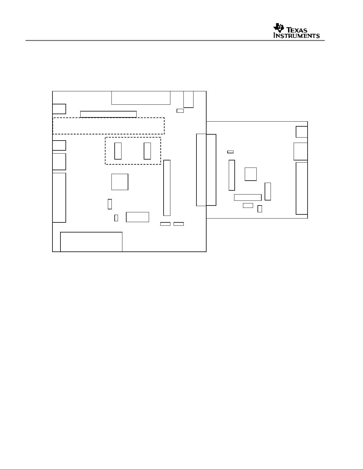
Figure 1 illustrates the various features available on the TVP5160EVM .
DB25 (I2C)
DB25 (I2C)
DB25 (I2C)
Analog Output
Analog Output
Analog Output
Tuner Interface
Tuner Interface
Tuner Interface
Composite
Composite
Composite
S-Video
S-Video
S-Video
YPbPr
YPbPr
YPbPr
(SD/ED)
(SD/ED)
(SD/ED)
Power
Power
Power
Down
Down
Down
Reset
Reset
Reset
VBI
VBI
VBI
Decoder
Decoder
Decoder
Interface
Interface
Interface
TVP5160
TVP5160
TVP5160
SDRAM
SDRAM
SDRAM
Power
Power
Power
Good
Good
Good
LED
LED
LED
Testpoints
Testpoints
Testpoints
5V
5V
5V
Power
Power
Power
Power
Power
Good
Good
LED
LED
120-pin Header Connector
120-pin Header Connector
120-pin Header Connector
120-pin Header Connector
120-pin Header Connector
ADV7311
ADV7311
Testpoints
Testpoints
I2C
I2C
Address
Address
Select
Select
Reset
Reset
Composite
Composite
S-Video
S-Video
YPbPr
YPbPr
(SD/ED)
(SD/ED)
SCART
SCART
SCART
2.1 Analog Inputs
The TVP5160EVM makes use of all the available inputs on the TVP5160 decoder. The
following inputs are available for use:
? Composite (CVBS)
? S-Video
? YPbPr (SD/ED)
? SCART (CVBS and component RGB)
? Tuner interface (CVBS)
? VBI decoder interface (analog/digital RGB)
NOTE: The S-Video (Y/C) input is shared with the SCART (CVBS and R) inputs and must not be
connected simultaneously.
FSS
I2C
FSS
I2C
FSS
Select
Select
Select
I2C
Address
Address
Address
Select
Select
Select
Figure 1. TVP5160EVM Block Diagram
Table 1 shows the pins used for the inputs described above.
4 TVP5160EVM User’s Guide
Page 5
Table 1. Analog Inputs and Pin Terminals
Input Type TVP5160 Pin(s)
CVBS VI_1
S-Video VI_3(Y), VI_9(C)
YPbPr VI_5(Y), VI_11(Pb), VI_8(Pr)
SCART VI_3(CVBS), VI_9(R), VI_6(G), VI_12(B)
Tuner interface (CVBS) VI_2
VBI decoder interface (analog RGB) VI_7(R), VI_4(G), VI_10(B)
2.2 Anti-Aliasing Filters
Each analog input has an anti-alias filter installed by default to ensure the input to the TVP5160
decoder is of the best quality and does not alias. The filters are elliptical in design in order to
minimize the cost and still provide the best roll-off. Details on the anti-aliasing filters, including
frequency response and the group delay , are provided in a separate application note.
The filter on any analog input may be bypassed by removing the 0-? resistors currently installed
(JP1-6, 9, 10) and shorting one of them across 1-2. Since the S-Video input is shared with the
SCART (CVBS and R), these inputs share the same anti-aliasing filters.
SLEU063
2.3 Analog Output
The analog output from the TVP5160 decoder is ma de available on the TVP5160EVM. The
output is buffered using a simple emitter follower and the output signal is automatically
determined by the TVP5160 decoder. If a CVBS is selected as the input, then the analog output
is the same looped-through CVBS output. If S-Video or YPbPr is the selected input, then only Y
is output since it contains the sync information. Typically , the analog output is used for VCR
record funct ions in some CE applications.
2.4 Tuner Interface
The tuner interface provides a method of connecting an analog TV tuner to the TVP5160EVM.
The expected output from the tuner module to the TVP5160EVM is baseband composite video.
Termination for the 75 -? input source is already provided on the TVP5160EVM tuner input. The
pinout of the tuner interface is provided in Table 2.
Table 2. Tuner Interface Pinout (H2)
Description Pin Number
CVBS output (from tuner) 10
SDA (I2C data) 29
SCL (I2C address) 31
GND 1-9, 11-28, 30, 32-36
D5V 37-40
To supply the tuner module, D5V supply and GND pins are provided. The I2C pins, SDA and
SCL, are connected to the I2C communications bus on the TVP5160EVM. Control of the tuner
module is available within the TVP5160EVM software as discussed later.
TVP5160EVM User’s Guide 5
Page 6

SLEU063
2.5 VBI Decoder Interface
This interface provides a method of connecting an external VBI decoder module to the
TVP5160EVM via the H3 and H4 headers. The VBI decoder may be a closed-caption decoder,
teletext decoder, or any other VBI decoder currently available on the market that provides the
same signals. The pinout of the VBI decoder interface is provided below.
Table 3. VBI Decoder Interface Pinout
Description H3 Pin Number H4 Pin Number
Tuner CVBS input (from tuner I/F) 1 CVBS input (from TVP5160EVM) 3 Analog RGB 11, 9, 7 (R, G, B) HSYNC 4 VSYNC 6 FSS (for analog overlay) 10 Digital RGB - 7, 9, 11 (DR, DG, DB)
SDA (I2C data) - 8
SCL (I2C address) - 10
FSO (for digital overlay) - 12
GND 2, 5, 8, 12 5, 6
D5V - 1-4
With this interface , there are two methods of overlaying the RGB character data output from the
VBI decoder onto the input signal to the TVP5160 decoder:
? Analog RGB overlay
? Digital RGB overlay
Separate sets of the RGB inputs are provided depending on which overlay method is preferred.
The analog RGB inputs are connected to the TVP5160 analog inputs as discussed in Section
2.1. The digital RGB inputs and FSO are connected to the digital R, G, and B inputs and FSO
which are shared with the C bus, C6-9, respect ively.
2.6 Test Points and Jumpers
Various test points are available on the TVP5160EVM for the user. This includes the various
power supplies as well as a few GND test points. The primary test-point header is H6 and
provides access to the video data, video clocks, I2C, 5 V, and GND.
There are three jumpers available on the TVP5160 board that configure the power down mode,
I2C address select, and the FSS select. Each jumper is set by default in its preferred state for
the TVP5160EVM. Next to each jumper on the TVP5160 board is the silkscreen that describes
the two states of the jumper configuration.
If the I2C address is changed on either the TVP5160 board or the ADV7311 board while the
TVP5160EVM is powered up, then that device will not recognize the new I2C address. The reset
button on the TVP5160EVM must be pressed and WinVCC4 must be reco nfigured for the new
I2C address.
6 TVP5160EVM User’s Guide
Page 7

2.7 SDRAM
On the TVP5160EVM , there are three SDRAM footprints: 50-pin, 54-pin, and 86-pin. These are
provided to accommodate the user’s choice of SDRAM that will be used in their final product.
By default, the TVP5160EVM is provided with 64-Mbit SDRAM (54TSOPII).
If the SDRAM is changed, then the SDRAM configuration register (0x59) will also need to be
updated with the correct memo ry size. This must be programmed before 3DYC or 3DNR is
enabled.
2.8 Common Board Interface
The TVP5160EVM uses a 120-pin connector to connect the TVP5160 board to the ADV7311
board. This interface shares all common signals including the I2C and the 5-V supply. The
purpose is to modularize the TVP5160 board and allow users to interface it to a variety of other
Texas Instruments products including triple video DACs, DVI transmitters, or to any other
platform that shares the same interface.
This connector sh ares all digital video data (Y[9:0], C[9:0]), all video clocks (SCLK, VS, HS,
GLCO, AVID, and FID), reset, I2C, and 5-V as mentioned above.
2.9 Video Encoder Analog Outputs
SLEU063
The analog outputs of the ADV7311 board include CVBS, S-Video, and YPbPr. All of the
outputs are available simultaneously. For evaluation purposes, it is recommended that the
YPbPr component video outputs be used in order to bypass the video decoder internal to the
display monitor.
TVP5160EVM User’ s Guide 7
Page 8
SLEU063
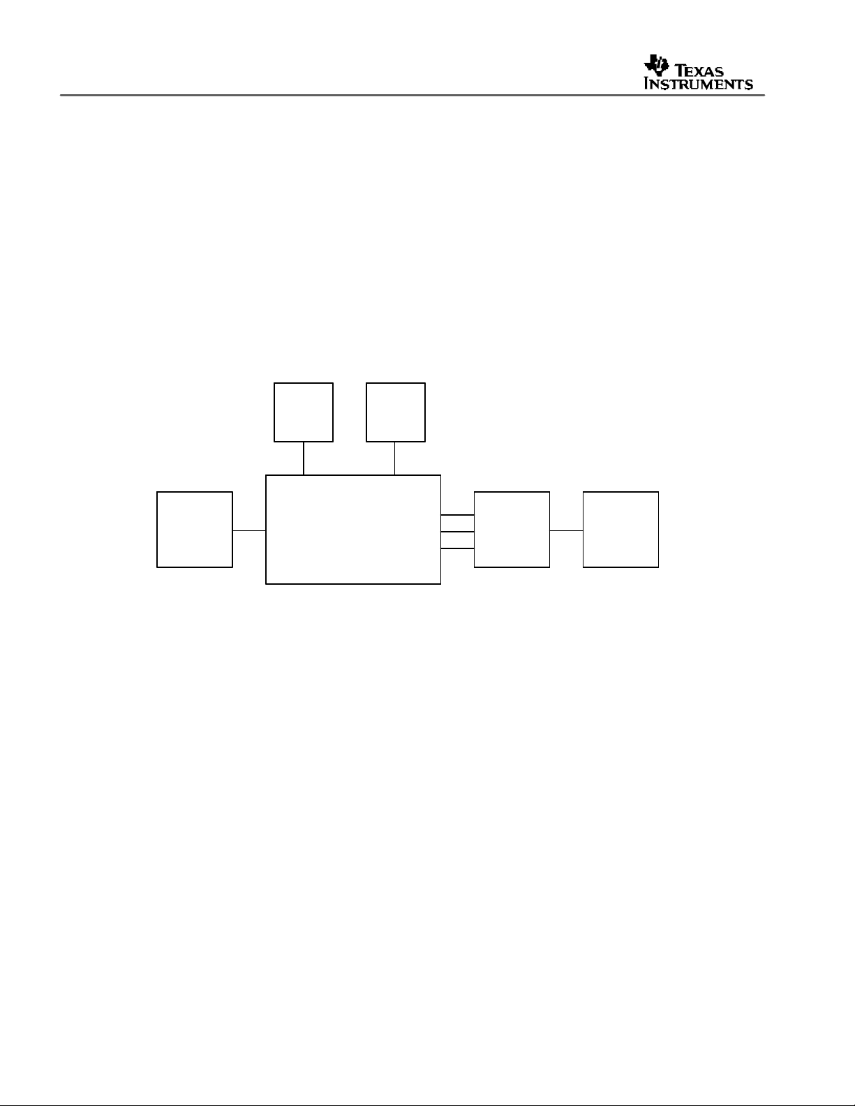
3 System Level Description
The system block diagram illustrated in Figure 2 provides an example of how the TVP5160EVM
may be used for evaluation. Typically , the analog input is a CVBS signal provided by a video
source such as a pattern generator or a DVD player running a test DVD.
The TVP5160EVM itself is configured with the provided 5-V supply and the parallel port cable.
The analog output is typically YPbPr to reduce the number of artifacts caused by backend
processing or re-encoding. These outputs are then fed into a high-end or studio-quality display
monitor such as a Sony Trinitron.
At the same time, the CVBS output from the encoder may also be fed into a video test
measurement system such as the Tektronix VM700. This allows various tests to be run and
also allows the user to analyze the video waveform or vectorscope.
PC
PC
5V
5V
Supply
Supply
Tektronix
Tektronix
Tektronix
TG2000
TG2000
Video
Video
Source
Source
CVBS
CVBS
TVP5160EVM
TVP5160EVM
Pb
Pb
Pr
Pr
Y
Y
NTSC/PAL
NTSC/PAL
Monitor
Monitor
CVBS
CVBS
Tektronix
VM700
VM700
Video
Video
Measurement
Measurement
Figure 2. TVP5160EVM System Level Block Diagram
8 TVP5160EVM User’s Guide
Page 9

4 Required Hardware and Equipment
The following lists the required hardware and equipment necessary to use the TVP5160EVM:
- TVP5160EVM (provided)
- Universal 5-V power supply (provided)
- Parallel cable (provided)
- Windows-based PC
- 1 composite RCA video cable
- 1 YPbPr component RCA video cable
- Video source (pattern generator, DVD player, etc)
- TV or display monitor that supports YPbPr component video inputs
SLEU063
TVP5160EVM User’s Guide 9
Page 10

SLEU063
5 Hardware Setup
The following describes how to set up the hardware for the TVP5160EVM.
1. Connect the TVP5160EVM boards together using the 120-pin board connector on
each board.
2. Connect a CVBS input to the TVP5160 board and a component cable to the YPbPr
outputs of the ADV7311 board.
NOTE: For evaluation it is recommended that the YPbPr component video outputs be
used in order to bypass the internal video decoder of the TV or video display.
3. Connect the parallel port cable from the TVP5160EVM to the PC.
NOTE: There are footprints for a dc jack and a DB25 connector on the ADV7311 board,
but the default power and I2C is provided by the TVP5160 board via the 120-pin
connector, P2.
4. Connect the 5-V power supply to the dc jack on the TVP5160 board. A green LED on
each board should now be lit.
10 TVP5160EVM User’s Guide
Page 11

6 Software Install ation
WinVCC4 is a Windows application that uses the PC parallel port to emulate I2C, providing
access to each device on the I2C bus. WinVCC4 makes use of CMD files, a text editable file
that allows preset video setups to be programmed easily.
This feature allows the user to easily set multiple I2C registers with the press of a button.
WinVCC4 also has “Property Sheets” for the TVP5160 which allows the user to control the I2C
registers with a GUI.
All necessary software for the TVP5160EVM is provided on the enclosed CD. The following
provides the steps required to install WinVCC4:
1. Insert the provided TVP5160EVM CD.
2. Install Port95NT.exe. This is the parallel port driver used by WinVCC4. This driver
must be installed and the PC must be rebooted before WinVCC4 will operate correctly.
3. Install Setup.exe. Click Next at all prompts and click Finish to complete the installation
process. This will install WinVCC4 onto the PC. No reboot is required.
4. Run WinVCC4.exe
SLEU063
NOTE: A shortcut to WinVCC4 should now be available on the desktop. WinVCC4 and
additional TVP5160 related documentation can also be found at Start->Programs->
TVP5160EVM Software.
TVP5160EVM User’s Guide 11
Page 12
SLEU063
7 WinVCC4 Quick Start
The following describes the steps to take within WinVCC4 in order to get video out of the
TVP5160EVM.
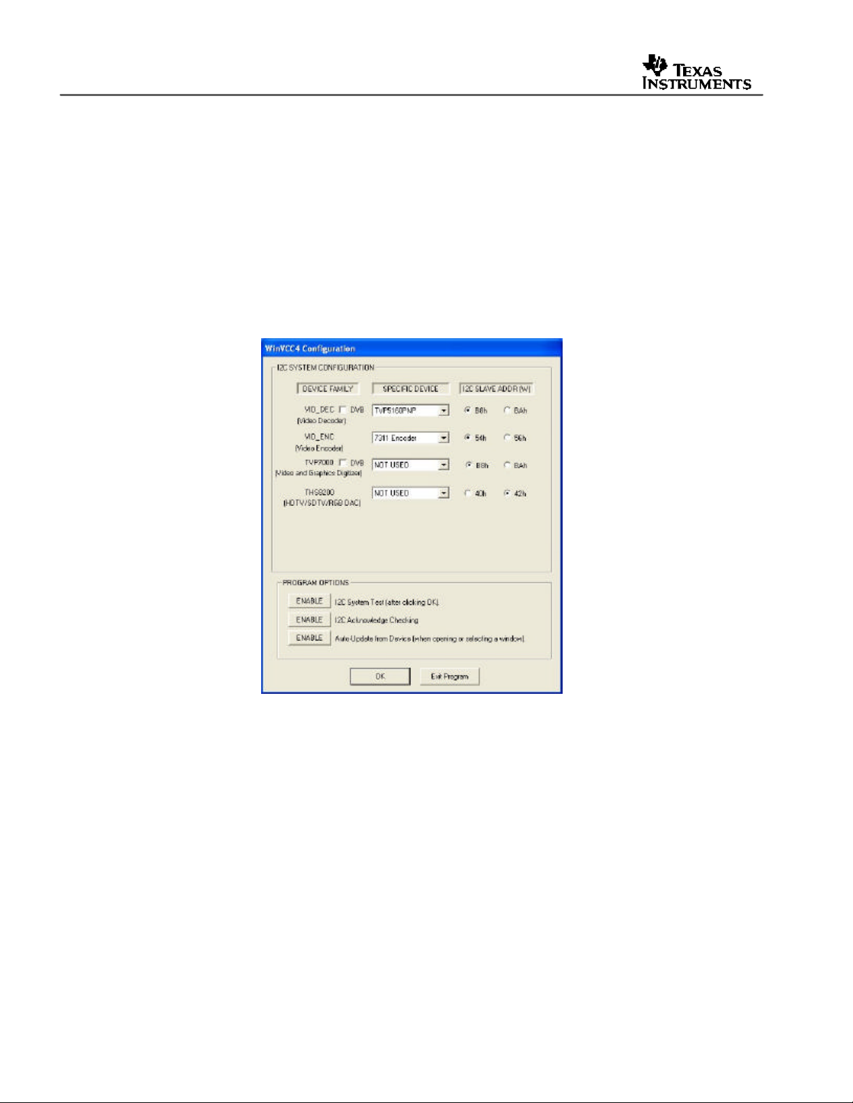
1. Once WinVCC4 is executed, the WinVCC4 Configuration screen appears. This dialog
box is used to configure the I2C bus. Next to VID_DEC, select the TVP5160 and ensure
the I2C address is set to 0xB8. This should match the I2C ADDR jumper on the
TVP5160 board.
NOTE: If WinVCC4 is running and the TVP5160 board I2C address is changed, power
must be cycled on the EVM.
Figure 3. WinVCC4 – I2C Configuration Screen
2. Next to VID_ENC, select the ADV7311 and ensure the I2C address is set to 0x54. This
should match the I2C ADDR jumper on the ADV7311 board.
3. Ensure that all other boxes are selected as Not Used and that all “Program Options”
buttons are set to Enabled. Click OK.
4. If there are no I2C communication issues, then the Real-Time Polling window will display
next. If there are I2C issues, an I2C Test Report box will display. Completely exit out of
WinVCC4, double check the parallel port cable connections, cycle power on the
TVP5160EVM and re-run WinVCC4.
12 TVP5160EVM User’s Guide
Page 13
SLEU063
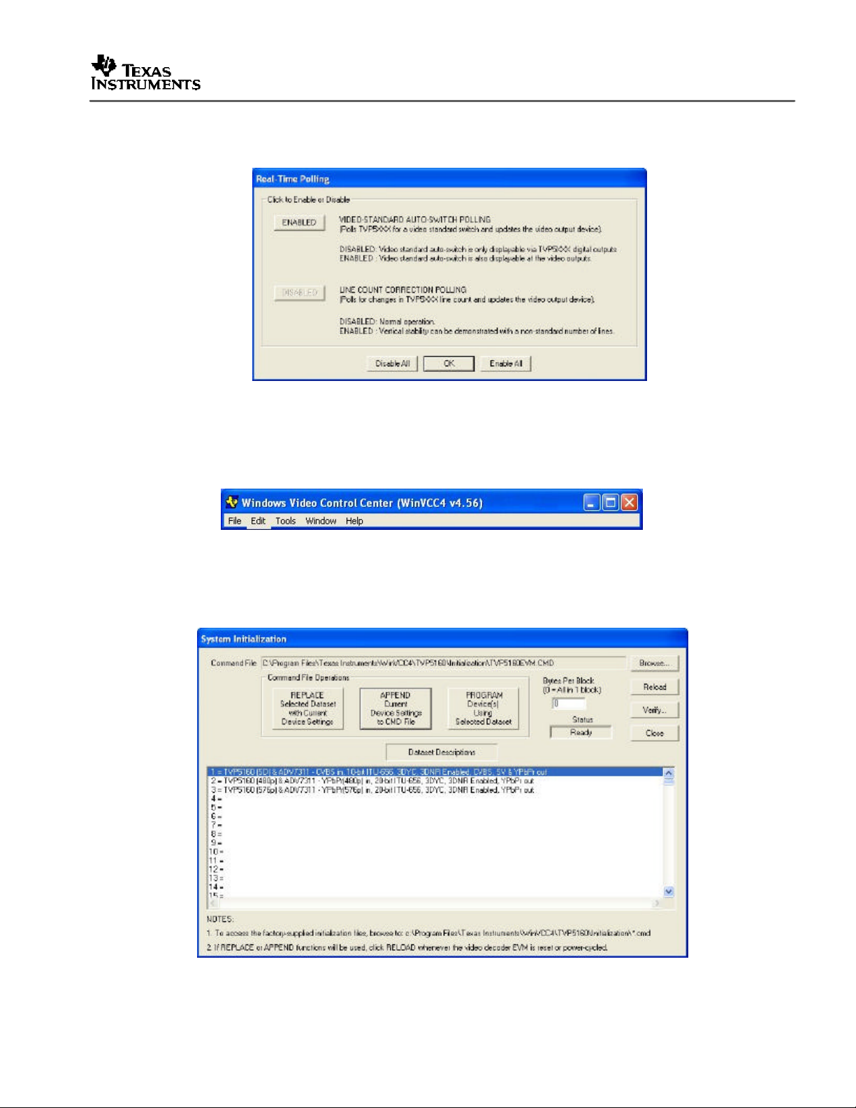
5. At the Real -Time Polling window, ensure that VIDEO-STANDARD AUTO_SWITCH
POLLING is enabled and click OK.
Figure 4. WinVCC4 – Real Time Polling Screen
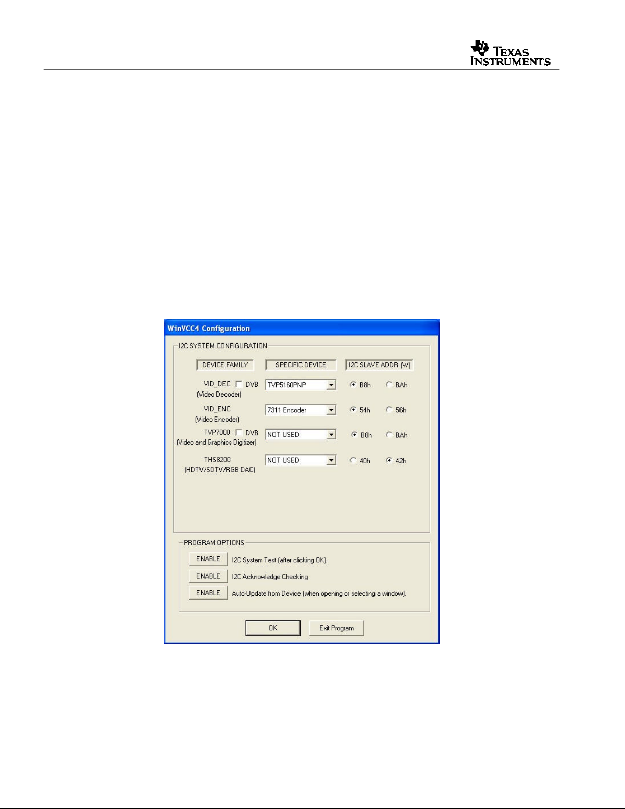
6. Load the provided TVP5160EVM.CMD file into WinVCC4 by clicking on Tools ->
System Initialization -> Browse . The CMD should be available by default as seen
below.
Figure 5. WinVCC4 – Main Screen
7. Click the “TVP5160 (SD) + ADV7311” dataset in the window and then click the Program
Dataset button to initialize the TVP5160EVM.
Figure 6. WinVCC4 – System Initialization
TVP5160EVM User’s Guide 13
Page 14

SLEU063
8. With a video source provided at the composite video input, video should be viewable on
the TV/display monitor. All ADV7311 outputs are enabled simultaneously.
NOTE: To ensure the TVP5160 is working properly, go to Video Status by clicking on
Edit -> Property Sheets -> TVP5160PNP -> Video Decoder Status and check the H/V/C
lock status and the video standard. This is only a check on the TVP5160 board and not
the ADV7311 board or the TV/display monitor.
14 TVP5160EVM User’s Guide
Page 15
8 WinVCC4 in Depth
The following describes how to use WinVCC4 in depth. It discusses various features and
screens which the user may encounter while evaluating the TVP5160EVM.
8.1 Starting WinVCC4
The Port95NT parallel port driver must be installed before using WinVCC4. WinVCC4 may be
started by clicking on Start->All Programs->TVP5160EVM Software->WinVCC4.
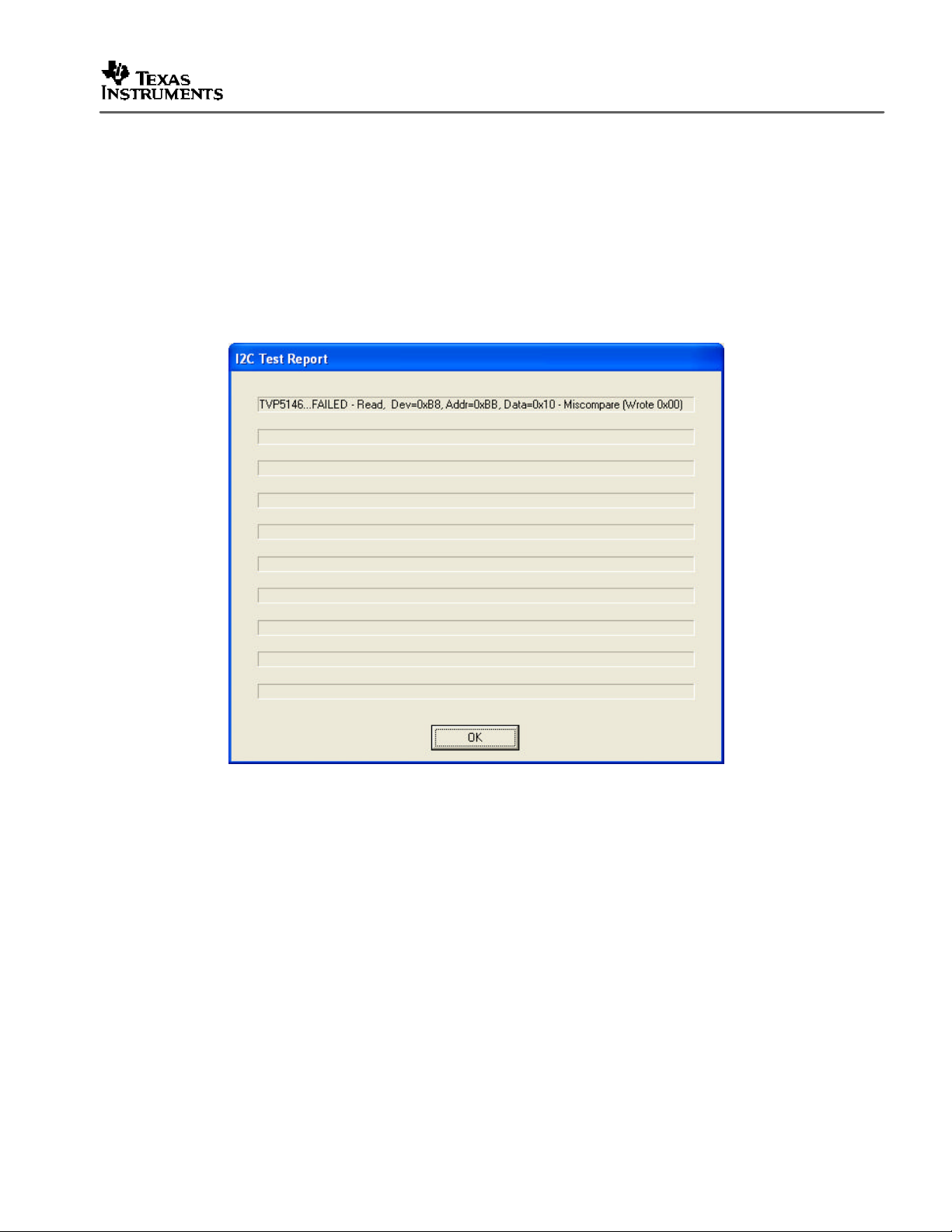
If the dialog shown in the figure below is displayed, it means one of two things:
1. WinVCC4 did not run to completion the last time it ran. In this case, click OK to exit
the program and restart WinVCC4.
2. There is more than one instance of WinVCC4 running at the same time. In this ca se,
click OK to exit the program. Then, press CTRL -ALT-DELETE to bring up the Task
Manager. Select and click End Task on all occurrences of WinVCC4 or WinVCC4
CONFIGURATION. Then restart WinVCC4.
SLEU063
Figure 7. WinVCC4 Multiple Occurrences Error Message
TVP5160EVM User’s Guide 15
Page 16
SLEU063
8.2 WinVCC4 Configuration Dialog Box
The WinVCC4 Configuration dialog box, as seen in Figure 8, should now be visible. This dialog
configures the I2C bus on the TVP5160EVM. All settings from this dialog box are stored in the
Windows registry and are restored the next time the program is started. After initial installation,
VID_DECTM will be set to TVP5160 and VID_ENC will be set to ADV7311.
The I2C slave address for each device must match the I2C slave address selected by jumpers on
the TVP5160EVM. These jumpers are set by the factory to use 0xB8 for the video decoder and
0x54 for the video encoder.
It is also important to select the correct specific devices. The TVP5160 and ADV7311 must be
selected for the TVP5160 EVM.
All Program Options must be enabled. Disabling these options is only required if you are
debugging a problem with the I2C bus itself.
Clicking OK begins I2C communication with the selected devices.
Figure 8. WinVCC4 I2C Address Configuration
16 TVP5160EVM User’s Guide
Page 17
8.3 I2C System Test
The I2C system test of selected registers runs immediately after closing the WinVCC4
Configuration dialog box with OK (unless the I2C system test program options button was
disabled).
If the I2C system test passes, then only a PASS message will appear. If the test failed, then a
dialog box like Figure 9 wi ll appear. See Section 9, Troubleshooting, for details on how to
resolve this issue.
The I2C system test can be run at anytime by clicking Run System I2C Test in the Tools menu.
SLEU063
8.4 Real-Time Polling
Real-time polling provides polling functions that execute in the background continuously, when
enabled via the Real-Time Polling dialog. There are two polling functions. The function that
applies to the TVP5160 decoder is VIDEO–STANDARD AUTO–SWITCH POLLING.
When the TVP5160 decoder detects a change in the input video standard, it automatically
switches to operation in the detected standard (which includes all necessary I2C register
initialization) for proper decoding of the input video. The ADV7311 encoder does not have this
feature. For this reason WinVCC4 must update the video encoder.
Figure 9. I2C System Failure
TVP5160EVM User’s Guide 17
Page 18

SLEU063
If the WinVCC4 autoswitch polling function is enabled, then the detected video standard status
from the TVP5160 decoder is polled until a change in the input video standard (or in the
TVP5160 sampling mo de) is detected. When a change is detected, the video encoder is
reprogrammed as needed for the detected standard. Using this feature, the video source can
change its video standard and the system will display using the new standard without user
intervention.
To enable autoswitch polling (recommended), the video -standard autoswitch polling function
must be enabled in the Real–Time Polling dialog box as shown in Figure 10. The Real–Time
Polling dialog can also be accessed once WinVCC4 is up and running by clicking Real–Time
Polling in the Tools menu.
Figure 10. Real-Time Polling Dialog Box
18 TVP5160EVM User’s Guide
Page 19

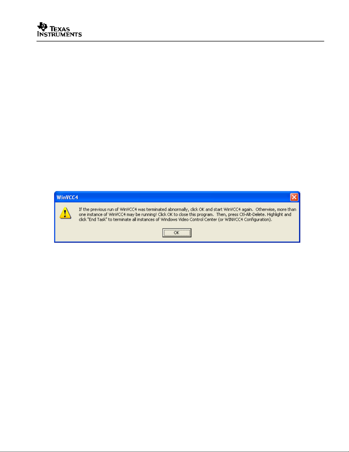
8.5 Main Menu
After closing the Real–Time Polling dialog, the main menu is displayed as shown in Figure 11.
The menus, which are used to operate WinVCC4, are File, Edit, Tools, Window, and Help. The
File menu’s only function is Exit, which terminates the program. The following table summarizes
the main menu contents.
Menu Contents
File Exit
Edit Register Map
Tools System Initialization
Window Allows selection of the active window. Multiple windows can be open at the same time.
Help Displays program version
SLEU063
Figure 11. WinVCC4 – Main Screen
Table 4. Main Menu Summary
TVP5160PNP
7311 Encoder Module Editor
Generic I2C Editor
Property Sheets
TVP5160PNP
7311 Encoder Module Editor
Real-time Polling
TV Tuner Control (FQ12xx series only)
Multiple-Byte I2C Transfers
Set I2C Bit Rate
Run System I2C Test
Run Continuous I2C Test
Read VBI FIFO
Capture Live VBI Data
TVP5160EVM User’s Guide 19
Page 20

SLEU063
8.5.1 System Initialization
Clicking System Initialization in the Tools menu displays the dialog shown below. This provides
the means for initializing the video decoder and/or video encoder for a particular video mode.
The details of the initialization are contained in the command file (with a CMD file extension).
The command file is loaded using the Browse… button. Once the command file is opened, a
text list displays descriptions of the individual data sets contained within the command file.
Click once on the desired data set description to select it. Click the Program Device(s) Using
Selected Dataset button to run the selected data set, which loads the devices via the I2C bus.
When the device initialization has completed, the status indicator reads Ready.
NOTE: If Ready does not display, then the devices are not initialized and the I2C bus is not
communicating. See Section 9, Troubleshooting, for possible solutions.
Click the Close button to close the dialog box. Each time the System Initialization dialog is
closed, the initialization file pathname and the data set selection number are saved in the
Windows™ registry to allow these settings to be retained for the next time WinVCC4 runs.
Figure 12. System Initialization
20 TVP5160EVM User’s Guide
Page 21

8.5.1.1 Adding a Custom Data Set
After you program the EVM via the System Initialization tool using the factory -supplied command
file, and by us ing the Property Sheets tool, you can customize the device register settings to suit
your needs. To save your custom settings:
1. Reopen the System Initialization dialog via the Tools menu.
2. Click the Append Current Device Settings to Command File button. A dialog
requesting a description of the new data set appears.
3. Optionally, click the drop-down box and select one of the existing descriptions.
4. Modify the description text or type your own description.
5. Click OK. All nondefault register values from the decoder and encoder will be
appended to the current command file as an additional data set.
Now, you can select your custom data set and send it with a press of the Program… button.
NOTE: The command file (.CMD) must be saved as plain text.
8.5.1.2 Command Files
The command file is a text file that can be generated using any common editor; however, it must
be saved as plain text. Command files are especially useful for quickly switching between the
various system configurations. These .CMD files are unrelated to the typical WindowsTM .CMD
files.
SLEU063
A default command file has been provided on the CD. This command file should contain most of
the desired setups. This command file is located at:
c:\Program Files\Texas Instruments\ WinVCC4\TVP5160\Initialization Files\Initialize.cmd
A command file can contain up to 250 data sets. A data set is a set of register settings to
initialize the video decoder and/or video encoder for a particular video mode. Each data set
includes a description that is displayed in one row of the dataset descriptions list. The register
settings may be located in the command file itself and/or may be stored in separate include
file(s) (with an .INC file extension) and be included into the command file using the INCLUDE
statement.
TVP5160EVM User’s Guide 21
Page 22

SLEU063
8.5.1.3 Example Command File
An example of one data set within a command file is shown below. Each command file may
contain individual write to register (WR_REG) commands.
BEGIN_DATASET // Dataset 1
DATASET_NAME,"TVP5160 (SD) & ADV7311 - CVBS in, 10-bit ITU-656, 3DYC, 3DNR Enabled,
CVBS, SV & YPbPr out"
WR_REG,VID_DEC,0x01,0xEE,0x01 // Holds processor in reset
WR_REG,VID_DEC,0x01,0xEA,0xB0 // Enables fast processor mode
WR_REG,VID_DEC,0x01,0xE9,0x00
WR_REG,VID_DEC,0x01,0xE8,0x63
WR_REG,VID_DEC,0x01,0xE0,0x01
WR_REG,VID_DEC,0x01,0xEE,0x00 // Releases processor reset
// TVP5160 I2C Registers - SD
WR_REG,VID_DEC,0x01,0x04,0x3F // Auto Switch Mask
WR_REG,VID_DEC,0x01,0x06,0x40 // Pedestal off
WR_REG,VID_DEC,0x01,0x34,0x11 // Outputs Enabled
WR_REG,VID_DEC,0x01,0x35,0x2A // GPIO =0; GLCO, AVID and FID Enabled
WR_REG,VID_DEC,0x01,0x36,0xAF // HS and VS Enabled
WR_REG,VID_DEC,0x01,0x75,0x1A // F & V Bit Control
WR_REG,VID_DEC,0x01,0x7F,0x01 // Analog Output Enabled
WR_REG,VID_DEC,0x01,0x59,0x07 // Enabled SDRAM and set SDRAM size
WR_REG,VID_DEC,0x01,0x0D,0x84 // Chrominance Processing Ctrl 1 Reg – 3DYC, 3DNR Enabled
// ADV7311 I2C Registers - NTSC, all DACs Output
WR_REG,0x54,0x01,0x01,0x08 // CLK Align Enabled, SD Oversampled
WR_REG,0x54,0x01,0x40,0x10 // Selects NTSC, SSAF Luma Filter
WR_REG,0x54,0x01,0x42,0x41 // Enables DAC Outputs , PrPb SSAF
WR_REG,0x54,0x01,0x44,0x06 // RTC Enabled
WR_REG,0x54,0x01,0x48,0x14 // Enables Double Buffering, SD 10-bit, DNR disabled
WR_REG,0x54,0x01,0x7C,0x02 // Global 10-bit enable
END_DATASET
1. The comment indicator is the double -slash //.
2. The command file is not case -sensitive and ignores all white-space characters.
3. All numbers can be entered as hexadecimal (beginning with 0x) or as decimal.
4. Every data set in a command file begins with BEGIN_DATASET and ends with
END_DATASET. The maximum number of datasets is 250.
5. The dataset text description is entered between double quotes using the
DATASET_NAME command. The enclosed text can be up to 128 characters in length.
This text appears in the System Initialization dialog when the command file is opened.
6. The INCLUDE command inserts the contents of an include file (with an .INC file
extension) in-line in place of the INCLUDE command. Therefore, the include file should
not contain the BEGIN_DATASET, END_DATASET, and DATASET_NAME commands.
NOTE: All included files must be located in the same directory as the command (CMD)
file.
22 TVP5160EVM User’s Guide
Page 23

SLEU063
7. The write to register command is written as follows:
WR_REG, <DeviceFamily>, <Number of data bytes (N)>, <subaddress>,
<Data1>,…, <DataN>
or
WR_REG, <Literal slave address>, <Number of data bytes (N)>, <subaddress>,
<Data1>,…, <DataN>
The valid device family mnemonics are:
VID_DEC for the video decoders
VID_ENC for the video encoders
THS8200 for the THS8200 device
WinVCC4 translates the device family mnemonic to the slave address that was selected
on the WinVCC4 Configuration dialog upon program startup. This eliminates having to
edit command files if the alternate slave address must be used.
If the literal slave address method is used, then the slave address entered will be used
directly. This method is normally used for programming the video encoder.
8. A delay may be inserted between commands using the WAIT command, which is written
as follows:
WAIT,<# milliseconds>
TVP5160EVM User’s Guide 23
Page 24

SLEU063
8.5.2 Register Editing
The next section describes the four available modes of register editing: Register Map Editor,
Encoder Module Editor, Generic I2C Register Editor, and Property Sheets. Each of these
functions can be selected from the Edit menu.
8.5.2.1 Register Map Editor
The register map editor, as shown in Figure 13, allows the display and editing of the entire used
register space of the device within a simple scrolling text box. To open this, click on Edit
Register Map in the Edit menu and click on the device type to edit. If the intended device type is
not shown, then use the Windows menu to activate the existing window.
Figure 13. Register Map Editor
24 TVP5160EVM User’s Guide
Page 25

SLEU063
Table 5. Register Map Editor Controls
Control Definition
Register Window Scrolling text box that displays the address and data for the I2C registers that are defined
for the device.
Address Edit Box This contains the I2C subaddress that will be accessed using the Write and Read
Data Edit Box This contains the data which will be written to or was read from the I2C subaddress.
Write Button Writes the byte in the Data Edit box to the address in the Address Edit box.
Read Button Reads the data from the address in the Address Edit box into the Data Edit box and the
Read All Button Reads all defined readable registers from the device and updates the register window.
Hex Button Converts all values in the register window and address and data edit boxes to
Dec Button Converts all values in the register window and address and data edit boxes to decimal.
Close Button Closes the dialog.
Loop Count Causes subsequent write or read operations to be performed N times. N is entered as a
Edit Indirect Registers Opens the indirect register editor of the TVP5160.
buttons. Clicking on a row selects an address, which then appears in the address edit
box.
NOTE: After clicking on a row, the Data Edit box contains the data that was in the
register window. The device has not yet been read.
The address up/down arrows are used to jump to the next/previous subaddress that is
defined for the device. If an address is not defined for the device, then it can still be
accessed by typing the subaddress in the Address Edit box.
The data up/down arrows incr/decr the data value by 1.
The I2C register is written to whether or not the data is different from the last time the
register was read.
register window.
hexadecimal.
NOTE: Multiple edit register map windows can be open at the same time (one for each
device). Use the Window menu to navigate.
decimal number from 1 to 999.
TVP5160EVM User’s Guide 25
Page 26

SLEU063
8.5.2.2 Encoder Module Editor
The encoder module editor, as shown in Figure 14, allows the display and editing of the video
encoder registers. This editor works like the Register Map Editor.
To open this, click on Edit Register Map in the Edit menu and click on Encoder Module.
Figure 14. Encoder Module Editor
26 TVP5160EVM User’s Guide
Page 27

8.5.2.3 Generic I2C Register Editor
The Generic I2C Editor, as shown in Figure 15, allows the display and editing of any device on
the I2C bus. This editor works like the Register Map Editor, except that the I2C slave address
must be entered and the Read All button is disabled.
To open this, click on Edit Register Map in the Edit menu and then click on Generic I2C.
The video encoder module registers can be edited using I2C subaddress 0x54 (default) or 0x56,
if the alternate slave address is being used.
SLEU063
Figure 15. Generic I2C Register Editor
TVP5160EVM User’s Guide 27
Page 28

SLEU063
8.5.2.4 Indirect Register Editor
The indirect register editor, as shown in Figure 16, allows the display and editing of the indirect
registers (or hardware registers) of the device.
To open this, first open the register map editor in the Edit menu for the TVP5160. Then, click
the Edit Indirect Registers button. The operation of the controls of the indirect register editor is
explained in Table 6.
Figure 16. Indirect Register Editor
Table 6. Indirect Register Controls
Control Definition
Base Address Selector The indirect registers use a 24-bit address internally. The base address selector
Base Address Edit Box This allows the 24-bit base address to be typed in directly.
Address Offset Edit Box This contains the lowest byte of the 24-bit internal address. The full 24-bit address
Data Edit Boxes This contains the 32-bit data word that will be written to or read from the indirect
Write Button Writes the (4) bytes in the Data Edit boxes starting at the 24-bit indirect address
Read Button Reads (4) consecutive data bytes starting at the 24-bit indirect address
Loop Count Edit Box Causes subsequent write or read operations to be performed N times. N is
Close Button Closes the dialog.
allows quick entry of the base address. The list contains base addresses for the
major functional blocks of the TVP5160 decoder.
is formed by adding the base address to the address offset.
The address up/down arrows increment/decrement the address offset by 4.
address. The LSB data is at the lowest address. The data is written/read LSB first.
The data up/down arrows increment/decrement the data value by 1.
BASE+OFFSET.
BASE+OFFSET to the Data Edit boxes.
entered as a decimal number from 1 to 999.
NOTE: The indirect register editor can remain open with other windows. Use the
Window menu to navigate.
28 TVP5160EVM User’s Guide
Page 29

8.5.3 Property Sheets
The Property Sheets represent the register data in a user-friendly format. The data is organized
by function, with each function having its own page and being selectable via tabs at the top.
To open this, click on Edit Property Sheets in the Edit menu and select the device type to edit.
When the property sheet function is started or whenever you tab to a different page, all readable
registers in the device are read from hardware to initialize the dialog pages. Values on the page
are changed by manipulating the various dialog controls as seen in Figure 17.
There are OK, Cancel, and Apply buttons at the bottom of each property page. These are
explained in detail below.
8.5.3.1 Reading the Register Map
The property sheets were designed so that the data displayed is always current. Certain actions
cause the entire register map to be read from the device and to update the property sheets.
This happens when:
1. Property sheets are initially opened.
2. When tabbing from one page to another.
3. When Read All is clicked.
SLEU063
4. When making the Property Sheets window the active window (by clicking on it).
5. When making a Register Map Editor window the active window (by clicking on it).
TVP5160EVM User’s Guide 29
Page 30

SLEU063
8.5.3.2 Auto–Update from Device
Items 4 and 5 above are referred to as the Auto–Update feature. Auto–Update can be disabled
by setting its program option button to DISABLED. This button is located on the initial dialog box
(WinVCC4 Configuration).
With Auto–Update enabled (default), the user can open both the Property Sheets and the
Register Map Editor at the same time. Changes made to the Property Sheets (and applied) are
updated in the register map window as soon as the Register Map window is clicked on. It also
works the other way; changes made in the Register Map Editor are updated in the Property
Sheets as soon as the Property Sheets window is clicked on.
Figure 17. Property Sheets
30 TVP5160EVM User’s Guide
Page 31

Table 7. Use of Property Sheet Controls
SLEU063
Dialog Control
Read–Only Edit Box Read status information N/A
Check Box Toggle a single bit After Apply
Drop–Down List Select from a text list After Apply
Edit Box Type a number After Apply
Edit Box with
Up/Down arrows
Slider Slide a lever Immediately
Pushbutton Initiate an action Immediately
Use up/down arrows or type a number Up/Down Arrows: Immediately
What Do I Do With It? When is Hardware Updated?
Type a number: After Apply
Table 8. Property Sheet Button Controls
Button Control Definition
OK Writes to all writeable registers whose data has changed. A register is flagged as changed if the
value to be written is different from the value last read from that address.
Closes the dialog.
Cancel Causes all changes made to the property page since the last Apply to be discarded. Changes made
to dialog controls with ‘immediate hardware update’ are not discarded, since they have already been
changed in hardware.
Does not write to hardware.
Closes the dialog.
Apply Writes to all writeable registers whose data has changed. A register is flagged as changed if the
value to be written is different from the value last read from that address.
TVP5160EVM User’s Guide 31
Page 32

SLEU063
9 Troubleshooting
This chapter discusses ways to troubleshoot the TVP5160EVM.
9.1 Troubleshooting Guide
If you are experiencing problems with the TVP5160EVM hardware or the WinVCC4 software,
see Table 9 for available solutions.
Table 9. TVP5160EVM Troubleshooting
Symptom Cause Solution
At startup, the error message
Cannot find DLL file
DLPORTIO.DLL appears.
Blank screen
No color GLCO pin is not set to output the
Screen colors are only magenta
and green.
Video standard auto–switch
does not work on the video
decoder side.
Video standard auto–switch
does not work on the video
encoder side.
The parallel port driver supplied with
the EVM has not been installed.
Wrong video input is selected. Go to Edit->Property Sheets->
Source is connected to the wrong input
connector.
YCbCr outputs or clock output is
disabled.
GLCO signal.
Wrong YCbCr output format. Go to Edit->Property Sheets->
Autoswitch masks are not set correctly. Go to Edit->Property Sheets->
Video decoder is not in auto–switch
mode.
Auto–switch polling is not enabled. Click Real–Time Polling in the Tools
Run Port95NT.EXE on the CD to
install the driver.
TVP5160, Analog Video page, select
the correct video input(s) and click
Apply.
(The Composite Video 1 input is
default.)
Connect source to the correct input
connector.
Go to Edit->Property Sheets->
TVP5160, Output Control, check the
Enable YCbCr Outputs and Enable
Clock Outputs check boxes and click
Apply.
Go to Edit->Property Sheets->
TVP5160, GPIO page, set the drop
down box labeled “GLCO/I2CA
Terminal” to Genlock Output and
click Apply.
TVP5160, Output Control, set the
YCbCr output format to 10-bit 4:2:2
ITU-R BT.656 with embedded syncs
mode and click Apply.
TVP5160, Mode Selection page,
check all standards to be included in
auto–switch processing and click
Apply.
Go to Edit->Property Sheets->
TVP5160, Mode Selection page, set
the drop–down box to Multi–Standard
and click Apply.
menu. Click Enable All and OK.
32 TVP5160EVM User’s Guide
Page 33

Table 10. I2C Troubleshooting
Symptom Cause Solution
No I2C
communication
I2C slave address is wrong. Close and restart WinVCC4. Choose the alternate slave
address in the WinVCC4 Configuration dialog.
Parallel cable is not connected from
PC parallel port to the EVM DB25
connector.
EVM is not powered on. The power supply must be plugged into a 100-V to 240-V/
Wrong type of parallel cable. Some parallel cables are not wired straight through pin-
PC parallel port mode is not set
correctly.
Device was placed in power –down
mode.
EVM was configured for an external
I2C master.
Still no I2C communication The PC may not be capable of operating in the required
Connect cable.
47-Hz to 63-Hz power source and the cord must be
plugged into the power connector on the EVM.
for-pin. Use the cable supplied with the EVM.
Reboot PC, enter BIOS setup program, set parallel port
LPT1 mode (Addr 378h) to ECP mode or bidirectional
mode (sometimes called PS/2 mode or byte mode). If
already set to one of these two modes, switch to the other
setting.
See Section 4.2.1.
Press the reset button on the TVP5160EVM.
Reinstall 0-? resistors R5 and R6. Control EVM using the
PC parallel port.
parallel port mode. This is true of some laptop computers.
Use a different computer, preferably a desktop PC.
SLEU063
When WinVCC4 is started and the WinVCC4 Configuration dialog box is closed with OK, the I2C
system test is performed (unless the I2C System Test program options button was disabled).
If the I2C system test fails, a dialog box will appear. Figure 18 reports that a read from TVP5160
failed, using slave address 0xB8, subaddress 0xBD. The data read was 0x00. The expected
data was 0x01.
After noting which device had a problem, click OK to continue. Next, the Corrective Action
Dialog box appears to help fix the problem.
TVP5160EVM User’s Guide 33
Page 34

SLEU063
Figure 18. I2C System Failure Dialog Box
9.2 Corrective Action Dialogs
After closing the I2C system test report dialog box, the dialog in Figure 19 appears.
Figure 19. Corrective Action Dialog Box
1. If the cable is NOT connected from the PC parallel port to the TVP5160EVM or if the EVM
power is not on:
a. Click NO.
b. The dialog shown in Figure 20 appears instructing you to correct the problem.
34 TVP5160EVM User’s Guide
Page 35

SLEU063
c. Correct the problem.
d. Click OK to continue. The real-time polling dialog should appear. See Section 3.2.3.
Figure 20. Corrective Action Required
2. If the cable is connected from the PC parallel port to the TVP5160EVM AND the EVM power is
on:
a. Click Yes.
b. The dialog shown in Figure 21 appears. This dialog appears if the PC parallel port mode
setting may need to be changed.
NOTE: Only run the PC BIOS setup program if the I2C communication problem cannot be
resolved in another way. (Correct slave address settings, reset or power cycle the EVM and/or
check that the device type selected was TVP5160).
c. Click OK to continue.
d. The real-time polling dialog ap pears. Click OK to close it and get to the main menu.
e. Click Exit in the File menu to exit the program.
f. See troubleshooting guide above.
Figure 21. Corrective Action Required
9.2.1 Setting the PC Parallel Port Mode
NOTE: Only run the PC BIOS setup program if the I2C commu nication problem cannot be
resolved in another way. (Correct slave address settings, reset or power cycle the EVM, and/or
check that the device type selected was TVP5160).
TVP5160EVM User’s Guide 35
Page 36

SLEU063
1. Restart the PC.
2. During the boot process, enter the BIOS setup program by pressing the required key
(usually the initial text screen tells you which key to press).
3. Find the place where the parallel port settings are made.
4. Set the parallel port LPT1 at address 378h to ECP mode or bidirectional mode
(sometimes called PS/2 mode or byte mode). If one of these two modes is already
selected, change to the opposite mode.
5. Exit and save changes.
9.2.2 General I2C Error Report
The error report shown in Figure 22 appears when an I2C error occurs at any time other than
after the I2C system test. In this example, there was an acknowledge error at slave address
0x54 (the video decoder module). The error occurred on Read Cycle Phase 1 on the device
(slave) address byte.
Figure 22. I2C Error
36 TVP5160EVM User’s Guide
Page 37

10 TVP5160EVM Schematics
This chapter contains the TVP5160EVM schematics.
SLEU063
TVP5160EVM User’s Guide 37
Page 38

ADV7311 Board
Revision 1.0
654321
D
Feb 2005
C
Connector
Connector
CONN_RESET
SCL
SDA
Y[9..0]
CLKIN
/HSYNC
/VSYNC
/BLANK
UV[9..0]
RTC
ADV7311 MODULE REV 1.0
SCL
SDA
I2C
/RESET
SCL
SDA
Y[9..0]
CLKIN
/HSYNC
/VSYNC
/BLANK
C[9..0]
RTC
I2C
ADV7311
ADV7311
Power
Power
RESET
CONN_RESET
D
C
G/Y
B/Pb
R/Pr
SV
DVI Tx
B
SCL
SDA
Testpoints
Testpoints
A
1 2 3 4 5 6
Y[9..0]
CLKIN
UV[9..0]
/HSYNC
/VSYNC
/BLANK
RTC
DVI Tx
CVBS
Title
ENCODER EVM - BLOCK DIAGRAM
Number RevisionSize
C
Date: 16-Feb-2005 Sheet of
File: C:\Userdata\EVM Design Files\MODULARIZED_EVMS\ADV7311EVM_MODULE_REV1.0\ADV7311EVM_MODULE_REV1.0.DdbDrawn By:
REV 1.0
B
A
Page 39

654321
D
D3_3V
C1
U2C
74AHC05
U2F
74AHC05
147
U2B
74AHC05
U2E
74AHC05
U2A
56
74AHC05
34
R2
2.2k
D3_3V
R8
2.2k
C
P3
1
14
2
15
3
16
4
17
5
18
6
19
7
20
8
21
9
22
10
23
11
24
12
25
13
DB25F
26 27
B
DB15
DB17
DB9
DB11
R4
2.2kR52.2k
0.1uF
R7
2.2k
2.2k
R1
13 12
1 2
11 10
U2D
74AHC05
R3
2.2k
R6
98
SCL
0
SCL
0
SDA
SDA
R9
D
C
B
A
Title
ENCODER EVM - I2C
Number RevisionSize
C
Date: 16-Feb-2005 Sheet of
1 2 3 4 5 6
File: C:\Userdata\EVM Design Files\MODULARIZED_EVMS\ADV7311EVM_MODULE_REV1.0\ADV7311EVM_MODULE_REV1.0.DdbDrawn By:
REV 1.0
A
Page 40

654321
D
D
OPTIONAL 5V, 3.0A DC INPUT
MAIN SUPPLY FROM CONNECTOR
D5V
P1
PJ-002BH
C
H1
1
3
2
HEADER 3
F1 FUSE
3
2
1
D1
ZENER
SS26
POWER ON LED (+5V)
D5V
R10
330
LED1
LED
B
L1
C2
47uF
Remove R8 to disable
RESET from Connector
CONN_RESET
R11
0
A5V
C3
22uF
D5V
C4
1uF
1
2
3
U1
IN
GND
EN
TPS76233
OUT
BYPASS
5
4
C5
0.01uF
A3_3VL2
C6
22uFC70.1uF
D3_3V
C8
22uF
C
RESET ON POWER UP
D3_3V
R12
100k
S1
PB
U3
1
CONTROL
/RESIN
CT
GND4/RESET
TLC7733IPW
VDD
SENSE
RESET
2
3
C9
1uF
C10 0.1uF
8
7
6
5
RESET
RESET
B
A
Title
ENCODER EVM - POWER
Number RevisionSize
C
Date: 16-Feb-2005 Sheet of
1 2 3 4 5 6
File: C:\Userdata\EVM Design Files\MODULARIZED_EVMS\ADV7311EVM_MODULE_REV1.0\ADV7311EVM_MODULE_REV1.0.DdbDrawn By:
REV 1.0
A
Page 41

654321
D
Y[9..0]
Y[9..0]
C
UV[9..0]
UV[9..0]
H2
Y0
1 2
Y1
3 4
Y2
5 6
Y3
7 8
Y4
9 10
Y5
11 12
Y6
13 14
Y7
15 16
Y8
17 18
Y9
19 20
HEADER 10X2
H3
UV0
1 2
UV1
3 4
UV2
5 6
UV3
7 8
UV4
9 10
UV5
11 12
UV6
13 14
UV7
15 16
UV8
17 18
UV9
19 20
HEADER 10X2
D
C
H4
1 2
3 4
TP1
TP
TP2
TP
TP
1
TP
1
5 6
7 8
9 10
11 12
HEADER 6X2
SDA
SCL
RTC
B
A
1 2 3 4 5 6
RTC
/HSYNC
/HSYNC
/VSYNC
/VSYNC
/BLANK
/BLANK
CLKIN
SDA
SCL
CLKIN
Title
ENCODER EVM - TESTPOINTS
Number RevisionSize
C
Date: 16-Feb-2005 Sheet of
File: C:\Userdata\EVM Design Files\MODULARIZED_EVMS\ADV7311EVM_MODULE_REV1.0\ADV7311EVM_MODULE_REV1.0.DdbDrawn By:
B
A
REV 1.0
Page 42

654321
D
D5VD5V
P2
30
5V
29
5V
28
GND
27
GND
26
GND
SCL
SCL
C
SDA
SDA
25
SCL/PHI_ACK
24
SDA/PHI_RWW
23
PHI_DS/RD
22
PHI_CS
21
PHI_A1
20
PHI_A0
19
PHI_D7
18
PHI_D6
17
PHI_D5
16
PHI_D4
15
PHI_D3
14
PHI_D2
13
PHI_D1
12
PHI_D0
11
GND
10
CLK5/M1
9
FPDAT/VSYA/M2
8
FFRSTW/CBFLAG
7
FSY/HC/HSYA/~BLNK
6
VGAV/SYNC_T
5
FFIE/CCVALID
4
FFWE/DVALID
3
FFRSTWIN/~SCLK
2
FFRE/DIG_H
1
FFOE/DIG_V
SAMTEC_TMMS_120PIN_F_RA
60
5V
59
5V
58
GND
57
GND
56
GND
55
AMXCLK
54
ALRCLK
53
ASCLK
52
AMCLK
51
GND
50
GPIO7
49
GPIO6
48
GPIO5
47
GPIO4
46
GND
45
GPIO3
44
GPIO2
43
GPIO1
42
GPIO0
41
INTREQ
40
GPCL
39
GND
38
ITRDY
37
SOGOUT
36
VACTIVE
35
D_SCLK
34
D_RDY
33
D_PREF
32
D_HS
31
D_VS
CONN_RESET
CONN_RESET
/HSYNC /VSYNC
/BLANK
/BLANK
D5V D5V
90
5V
89
GND
88
GND
87
RCr9
86
RCr8
85
RCr7
84
RCr6
83
RCr5
82
RCr4
81
RCr3
80
RCr2
79
RCr1
78
RCr0
77
GND
76
D9
75
D8
74
D7
73
D6
72
D5
71
D4
70
D3
69
D2
68
D1
67
D0
66
GND
65
RESET
64
PALI
63
HSYNC
62
AVID
61
PREF
UV[9..0]
Y[9..0]
RTC
/VSYNC/HSYNC
CLKIN
RTC
CLKIN
UV[9..0]
Y[9..0]
UV9
UV8
UV7
UV6
UV5
UV4
UV3
UV2
UV1
UV0
Y9
Y8
Y7
Y6
Y5
Y4
Y3
Y2
Y1
Y0
120
5V
119
GND
118
GND
117
BCb9
116
BCb8
115
BCb7
114
BCb6
113
BCb5
112
BCb4
111
BCb3
110
BCb2
109
BCb1
108
BCb0
107
GND
106
GY9
105
GY8
104
GY7
103
GY6
102
GY5
101
GY4
100
GY3
99
GY2
98
GY1
97
GY0
96
GND
95
FID
94
GLCO
93
VSYNC
92
PCLK
91
SCLK
D
C
B
A
Title
ENCODER EVM - CONNECTOR
Number RevisionSize
C
Date: 16-Feb-2005 Sheet of
1 2 3 4 5 6
File: C:\Userdata\EVM Design Files\MODULARIZED_EVMS\ADV7311EVM_MODULE_REV1.0\ADV7311EVM_MODULE_REV1.0.DdbDrawn By:
REV 1.0
B
A
Page 43

654321
D3_3V
C12
C11
0.1uF
0.1uF
D
CLKIN
/BLANK
/VSYNC
/HSYNC
Y[9..0]
C
B
C[9..0]
SCL
SDA
A
A3_3V
C13
0.1uF
C14
0.1uF
I2C ADDRESS SELECTION
1-2 Base Addr 0x56
CVBS
R15
604
NO POP
2-3 Base Addr 0x54 - Default
ALSB
R13
10k
R14
10k
RTC
D3_3V
2 JP1
A3_3V
A3_3V
D3_3V
A3_3V
A3_3V
R24
1.1k
R33
4.7k
R47
4.99k
13
JMP3
SV_Y
R16
604
NO POP
SV_C
R25
604
NO POP
U10
1
V+
3
2
/RESET
I2C
COMP1
COMP2
V-
AD1580
NC
Pr/R
R48
300
Y/G
R34
300
Pb/B
R35
300
C25
0.1uF
C33
4.7uF
C41
0.1uF
C42
0.1uF
CLKIN
/BLANK
/VSYNC
/HSYNC
Y[9..0]
Y0
Y1
Y2
Y3
Y4
Y5
Y6
Y7
Y8
Y9
D3_3V A3_3V
1
2
Y0
3
Y1
4
Y2
5
Y3
6
Y4
7
Y5
8
Y6
9
Y7
10
11
12
Y8
13
Y9
14
C0
15
C1
16
C2
C3
C4
C5
C6
C7
C8
C9
C[9..0]
SCL
SDA
1 2 3 4 5 6
CLKIN
63
64
U9
GND_IO
CLKIN_B
VDD_IO
Y0
Y1
Y2
Y3
Y4
Y5
Y6
Y7
VDD
DGND
Y8
Y9
C0
C1
C2
C317C418I2C19ALSB20SDA21SCLK22/P_HSYNC23/P_VSYNC24/P_BLANK25C526C627C728C829C930RTC_SCR_TR31CLKIN_A
ADV7311
/HSYNC
SCL
SDA
ALSB
I2C
56
57S558S659S760S861S962
VDD
DGND
/VSYNC
/BLANK
EXT_LF
/VSYNC
/HSYNC
49
50S051S152S253S354S455
/S_VSYNC
/S_HSYNC
/S_BLANK
32
RSET1
RSET2
RSET1
VREF
COMP1
DAC A
DAC B
DAC C
VAA
AGND
DAC D
DAC E
DAC F
COMP2
RSET2
EXT_LF
/RESET
C40
3.9nF
C32
820pF
R44
3.01k
R45
3.01k
48
/BLANK
47
RSET1
46
VREF
45
COMP1
44
CVBS
43
SV_Y
42
SV_C
41
40
39
Y/G
38
Pb/B
37
Pr/R
36
COMP2
35
RSET2
34
EXT_LF
33
/RESET
CLKIN
A3_3V
R46
680
C17
NO POP
L3
10uH
C15
C18
NO POP
L4
10uH
C16
C27
NO POP
L5
10uH
C26
48
U8A
3
AD8062
2
3
2
3
2
1
VAA2
48
U6A
AD8062
1
VAA3
48
U7A
AD8062
1
VAA4
R17
C19
604
22pF
R18
C20
604
22pF
R26
C28
604
22pF
L10
75
R49
1.2uH
C43
NO POP
L6
75
R36
1.2uH
C34
NO POP
L7
75
R37
1.2uH
C35
NO POP
48
U4A
AD8062
3
2
C21
NO POP
R20
R19
560
3
2
C22
NO POP
R29
560
R28
560
5
6
C29
R30
560
R27
560
L11
0
C44
270pF
L8
0
C36
270pF
L9
0
C37
270pF
560
48
8 4
NO POP
VAA1
U5A
AD8062
U5B
AD8062
R21
1
75
C23
0.1uF
1uF
R22
1
75
R31
7
75
VAA1
C30
0.1uF
1uF
5
R50
6
75
R51
560
5
R38
6
75
R40
560
5
R39
6
75
R41
560
C24
R32
C31
C45
NO POP
R52
560
C38
NO POP
R42
560
C39
NO POP
R43
560
A5V
R23
0
A5V
0
U8B
AD8062
7
VAA2
0
8 4
U6B
AD8062
7
8 4
U7B
AD8062
7
8 4
R53
C46
C49
0.1uF
1uF
VAA3
0
R54
C47
C50
0.1uF
1uF
VAA4
0
R55
C48
C51
0.1uF
1uF
Title
ENCODER EVM - ADV7311
Number RevisionSize
C
Date: 16-Feb-2005 Sheet of
File: C:\Userdata\EVM Design Files\MODULARIZED_EVMS\ADV7311EVM_MODULE_REV1.0\ADV7311EVM_MODULE_REV1.0.DdbDrawn By:
CVBS
RCA
2
1
1
5
6
7
2
A5V
YPBPR
RCA_RGB
2
1
4
A5V
3
6
5
A5V
34
SV
SVIDEO_0
D
C
B
A
REV 1.0
Page 44

654321
C:\Userdata\EVM Design Files\MODULARIZED_EVMS\TVP5160EVM\TVP5160EVM_MODULE_REV2.0\TVP5160EVM_MODULE_REV 2.0.ddb
TVP5160EVM Rev 2.0
Revision 2.0
D
AOUT
Feb 2005
Tuner
CVBS
C
Y/G
Pb/B
B
Pr/R
SV
Tuner Interface
Tuner Interface
Anti-Aliasing Filters
Anti-Aliasing Filters
CVBS_OUT
Y/G_OUT
Pb/B_OUT
Pr/R_OUT
SCRT_CVBS_IN
SCRT_GRN_IN
SCRT_BLUE_IN
SCRT_RED_IN
SCRT_GRN_OUT
SCRT_BLUE_OUT
TUNER_CVBS
CVBS_IN
Y_IN
C_IN
Y_OUT
C_OUT
Y/G_IN
Pb/B_IN
Pr/R_IN
SCL
SDA
I2C
I2C
TVP5160
TVP5160
TUNER_CVBS
CVBS_IN
CVBS_OUT
Y_IN
C_IN
Y_OUT
C_OUT
Y/G_IN
Pb/B_IN
Pr/R_IN
Y/G_OUT
Pb/B_OUT
Pr/R_OUT
SCRT_CVBS_IN
SCRT_GRN_IN
SCRT_BLUE_IN
SCRT_RED_IN
SCRT_GRN_OUT
SCRT_BLUE_OUT
VBI Decoder Interface
VBI Decoder Interface
CVBS_IN
T_CVBS
ANALOG_OUT
A[11..0]
DQ[15..0]
BA1
BA0
CLK
RED
GREEN
BLUE
A_RED
A_BLUE
A_GREEN
RAS#
CAS#
FSS_RGB
FSS_RGB
/CS
WE#
DQM
SCL
SDA
SCL
SDA
VSYNC
DRDGDB
FSO
HSYNC
DBDGDR
SCART_VIDSTAT
SCART_CVBS_OUT
SCL
SDA
FSO
/RESET
C[9..0]
Y[9..0]
DATACLK
HS_CS
VS_VBLNK
AVID
FID
GLCO
INTREQ_OUT
SCART_DATA
SCART_CLK
Y[9..0]
Testpoints
Testpoints
C[9..0]
DATACLK
Power
Power
HSYNC
VSYNC
FID
AVID
/RESET
GLCO
INTREQ_TP
SCL
SDA
Connector
Connector
SCART_CLK
SCART_DATA
SCART_VIDSTAT
SCART_CVBS_OUT
SCL
SDA
/RESET
C[9..0]
Y[9..0]
DATACLK
HSYNC
VSYNC
AVID
FID
GLCO
INTREQU
D
C
B
SCART
A
1 2 3 4 5 6
/CS
/WE
/CAS
DQM
TSOPII-50 SDRAM
TSOPII-50 SDRAM
/RAS
BA0
CLK
DQ[15..0]
AQ[11..0]
BA0
CLK
DQ[15..0]
AQ[11..0]
TSOPII-54 SDRAM
TSOPII-54 SDRAM
BA1
/RAS
/CAS
/WE
DQM
/CS
BA0
CLK
DQ[15..0]
AQ[11..0]
TSOPII-86 SDRAM
TSOPII-86 SDRAM
BA1
/RAS
/CAS
/WE
DQM
/CS
Title
TVP5160EVM - BLOCK DIAGRAM
Number RevisionSize
B
Date: 16-Feb-2005 Sheet of
File:
Drawn By:
A
REV 2.0
Page 45

654321
D
D3_3V
T0
C
P3
DB25
B
1
1
14
2
15
3
16
4
17
5
18
6
19
7
20
8
21
9
22
10
23
11
24
12
25
13
26 27
T1
NACK
TP
TP
1
1
T2
POUT
TP
DB15
DB17
DB9
DB11
TP
TP
1
1
R53
R54
2.2k
2.2k
0.1uF
C1
R7
2.2k
2.2k
R8
U2C
74AHC05
U2F
13 12
74AHC05
147
U2A
1 2
74AHC05
U2B
74AHC05
U2E
11 10
74AHC05
R24
2.2k
56
D3_3V
R9
2.2k
34
U2D
74AHC05
R52
2.2k
R6
98
0
0
R5
SDA
SCL
SDA
D
C
B
A
Title
TVP5160EVM - I2C
Number RevisionSize
C
Date: 16-Feb-2005 Sheet of
1 2 3 4 5 6
File: C:\Userdata\EVM Design Files\MODULARIZED_EVMS\TVP5160EVM\TVP5160EVM_MODULE_REV2.0\TVP5160EVM_MODULE_REV 2.0.ddbDrawn By:
REV 2.0
A
Page 46

654321
D
D5V
H2
C
TUNER_CVBS
12
34
56
78
910
1112
1314
1516
1718
1920
2122
2324
2526
2728
2930
3132
3334
3536
3738
3940
SAMTEC SSW-120-02-G-D
SDA
SCL
D
C
B
A
Title
TVP5146EVM - TV TUNER INTERFACE
Number RevisionSize
C
Date: 16-Feb-2005 Sheet of
1 2 3 4 5 6
File: C:\Userdata\EVM Design Files\MODULARIZED_EVMS\TVP5160EVM\TVP5160EVM_MODULE_REV2.0\TVP5160EVM_MODULE_REV 2.0.ddbDrawn By:
REV 2.0
B
A
Page 47

654321
C:\Userdata\EVM Design Files\MODULARIZED_EVMS\TVP5160EVM\TVP5160EVM_MODULE_REV2.0\TVP5160EVM_MODULE_REV 2.0.ddb
D
D5V
C
T_CVBS
R60
CVBS_IN HSYNC
BLUE
GREEN
RED
H3
0
1 2
3 4
5 6
7 8
9 10
11 12
SAMTEC SSW-106-02-G-D
VSYNC
FSS_RGB
H4
1 2
3 4
DR
DG
DB FSO
5 6
7 8
9 10
11 12
SAMTEC SSW-106-02-G-D
SDA
SCL
D
C
B
A
Title
B
A
TVP5160EVM - VBI DECODER INTERFACE
Number RevisionSize
B
Date: 16-Feb-2005 Sheet of
1 2 3 4 5 6
File:
Drawn By:
REV 2.0
Page 48

654321
C:\Userdata\EVM Design Files\MODULARIZED_EVMS\TVP5160EVM\TVP5160EVM_MODULE_REV2.0\TVP5160EVM_MODULE_REV 2.0.ddb
D
D
COMPONENT - YPbPr CVBS & S-VIDEO SCART - CVBS & RGB (RED & CVBS shared w/ SV)
C3 5.6pF
1.8uH
Y/G_IN Y/G_OUT
Y/G_IN Y/G_OUT
C
Pr/R_IN
Pr/R_IN Pr/R_OUT
L1
C7
220pF
C6 8.2pF
2.2uH
L2
C8
330pF
C21 8.2pF
C9
220pF
C10
330pF
Pr/R_OUT
CVBS_IN CVBS_OUT
CVBS_IN CVBS_OUT
Y_IN
Y_IN Y_OUT
C4 5.6pF
1.8uH
L3
C12
220pF
C11 8.2pF
2.2uH
L4
C13
330pF
C24 8.2pF
C14
220pF
C15
330pF
Y_OUT
C16 8.2pF
2.2uH
SCRT_GRN_IN SCRT_GRN_OUT
SCRT_BLUE_IN SCRT_BLUE_OUT
SCRT_GRN_IN
SCRT_BLUE_IN
L6
C18
330pF
C27 8.2pF
L9
C29
330pF
2.2uH
SCRT_GRN_OUT
C20
330pF
SCRT_BLUE_OUT
C31
330pF
C
2.2uH
Pb/B_IN
Pb/B_IN Pb/B_OUT
B
L7
C22
330pF
C23
330pF
Pb/B_OUT
C_IN
C_IN C_OUT
L8
C25
330pF
2.2uH
C26
330pF
C_OUT
B
NOTE: SV- (Y/C) is shared with SCART - (CVBS/RED)
These anti-aliasing filters are used for both sets of inputs.
A
Title
A
TVP5160EVM - ANTI-ALIASING FILTERS
Number RevisionSize
B
Date: 16-Feb-2005 Sheet of
1 2 3 4 5 6
File:
Drawn By:
REV 2.0
Page 49

654321
D
D
5V, 3.0A DC INPUT
D5V
P1
PJ-002BH
F1 FUSE
H1
1
3
2
3
2
1
HEADER 3
D1
ZENER
SS26
1 2
L11
C33
47uF
A5V
C34
22uF
TVP5160 POWER SUPPLY
VOUT1 IS 3.3V 1A
VOUT2 IS 1.8V 2A
R20
C37
0.1uF
C38
0.1uF
249k
U8
1
GND
VIN1A
VIN1B
NC
/MR
/EN1
/EN2
/RESET
GND
VIN2A
VIN2B
GND
GND
VOUT1A
VOUT1B
VSENSE1/FB1
PG1
PG2
VSENSE2/FB2
VOUT2A
VOUT2B
GND
PP
25
NC
NC
2
3
4
5
6
7
8
9
10
11
12
TPS70451
C
POWER ON LED (+5V)
D5V
R19
330
LED1
LED
D5V
C35
22uF
C36
22uF
R10
0
24
23
22
21
20
R21 249k
19
18
17
R22 249k
16
15
14
13
0
R11
NO POP
R12
R61
NO POP
L12
C39
47uF
L14
L13
L15
C48
47uF
A3_3V
C40
C43
22uF
0.1uF
C
D3_3V
C41
C44
22uF
0.1uF
D1_8V
C49
C50
22uF
0.1uF
A1_8V
C42
C45
22uF
0.1uF
RESET ON POWER UP
D3_3V
B
A
1 2 3 4 5 6
R23
100k
RESET
RESET
U3
1
CONTROL
/RESIN
CT
GND4/RESET
TLC7733IPW
VDD
SENSE
RESET
2
3
C46
1uF
C47 0.1uF
8
7
6
5
/RESET
/RESET
Title
TVP5160EVM - POWER
Number RevisionSize
C
Date: 16-Feb-2005 Sheet of
File: C:\Userdata\EVM Design Files\MODULARIZED_EVMS\TVP5160EVM\TVP5160EVM_MODULE_REV2.0\TVP5160EVM_MODULE_REV 2.0.ddbDrawn By:
REV 2.0
B
A
Page 50

C:\Userdata\EVM Design Files\MODULARIZED_EVMS\TVP5160EVM\TVP5160EVM_MODULE_REV2.0\TVP5160EVM_MODULE_REV 2.0.ddb
D3_3V
654321
C51
0.1uF
D
C
B
C52
0.1uF
C53
0.1uF
C54
0.1uF
C55
0.1uF
C56
0.1uF
DQ[15..0]
DQ[15..0]
D3_3V
U4
1
VDD
DQ0
DQ1
DQ2
DQ3
DQ4
DQ5
DQ6
DQ7 DQ8
DQM
DQM
/WE
/WE
/CAS
/CAS
/RAS
/RAS
/CS
/CS
BA0
BA0
AQ10
AQ0
AQ1
AQ2
AQ3 AQ4
2
DQ0
3
DQ1
4
VSSQ
5
DQ2
6
DQ3
7
VDDQ
8
DQ4
9
DQ5
10
VSSQ
11
DQ6
12
DQ7
13
VDDQ
14
DQML
15
WE_
16
CAS_
17
RAS_
18
CS_
19
BA
20
A10
21
A0
22
A1
23
A2
24
A3
25
VDD
SDRAM_50TSOPII
VSS
DQ15
DQ14
VSSQ
DQ13
DQ12
VDDQ
DQ11
DQ10
VSSQ
DQ9
DQ8
VDDQ
NC
DQMH
CLK
CKE
NC
A9
A8
A7
A6
A5
A4
VSS
D
50
49
48
47
46
45
44
43
42
41
40
39
38
37
36
35
34
33
32
31
30
29
28
27
26
DQ15
DQ14
DQ13
DQ12
DQ11
DQ10
DQ9
DQM
CLK
AQ9
AQ8
AQ7
AQ6
AQ5
C
CLK
B
A
1 2 3 4 5 6
AQ[11..0]
AQ[11..0]
Title
TVP5160EVM - SDRAM 50-PIN TSOP II
Number RevisionSize
B
Date: 16-Feb-2005 Sheet of
File:
Drawn By:
A
REV 2.0
Page 51

C:\Userdata\EVM Design Files\MODULARIZED_EVMS\TVP5160EVM\TVP5160EVM_MODULE_REV2.0\TVP5160EVM_MODULE_REV 2.0.ddb
D3_3V
654321
C57
0.1uF
D
C
B
C58
0.1uF
C59
0.1uF
C60
0.1uF
C61
0.1uF
C62
0.1uF
C63
0.1uF
C64
0.1uF
DQ[15..0]
C65
0.1uF
DQ[15..0]
C66
0.1uF
C67
0.1uF
DQ0
DQ1
DQ2
DQ3
DQ4
DQ5
DQ6
DQ7 DQ8
DQM
/WE
/WE
/CAS
/CAS
/RAS
/RAS
/CS
/CS
AQ11
BA0
BA0
BA1
BA1
AQ10
AQ0
AQ1
AQ2 AQ3
D3_3V
C68
0.1uF
U5
1
2
3
4
5
6
7
8
9
10
11
12
13
14
15
16
17
18
19
20
21
22
23
24
25
26
27
28
29
30
31
32
33
34
35
36
37
38
39
40
41
42
43
SDRAM_86TSOPII
VDD
D0
VDDQ
D1
D2
VSSQ
D3
D4
VDDQ
D5
D6
VSSQ
D7
NC
VDD
DQM0
/WE
/CAS
/RAS
/CS
A11
BA0
BA1
A10/AP
A0
A1
A2
DQM2
VDD
NC
D16
VSSQ
D17
D18
VDDQ
D19
D20
VSSQ
D21
D22
VDDQ
D23
VDD
VSS
D15
VSSQ
D14
D13
VDDQ
D12
D11
VSSQ
D10
D9
VDDQ
D8
NC
VSS
DQM1
NC
NC
CLK
CKE
A9
A8
A7
A6
A5
A4
A3
DQM3
VSS
NC
D31
VDDQ
D30
D29
VSSQ
D28
D27
VDDQ
D26
D25
VSSQ
D24
VSS
D
86
85
84
83
82
81
80
79
78
77
76
75
74
73
72
71
70
69
68
67
66
65
64
63
62
61
60
59
58
57
56
55
54
53
52
51
50
49
48
47
46
45
44
DQ15
DQ14
DQ13
DQ12
DQ11
DQ10
DQ9
DQMDQM
CLK
AQ9
AQ8
AQ7
AQ6
AQ5
AQ4
C
CLK
B
A
1 2 3 4 5 6
R4
330
AQ[11..0]
AQ[11..0]
Title
TVP5160EVM - SDRAM 86-PIN TSOP II
Number RevisionSize
B
Date: 16-Feb-2005 Sheet of
File:
Drawn By:
A
REV 2.0
Page 52

C:\Userdata\EVM Design Files\MODULARIZED_EVMS\TVP5160EVM\TVP5160EVM_MODULE_REV2.0\TVP5160EVM_MODULE_REV 2.0.ddb
D3_3V
654321
C69
0.1uF
D
C
B
C70
0.1uF
C71
0.1uF
C72
0.1uF
C73
0.1uF
C74
0.1uF
C75
0.1uF
DQ[15..0]
DQ[15..0]
D3_3V
U6
Reference
1
Vcc
DQ0
DQ1
DQ2
DQ3
DQ4
DQ5
DQ6
DQ7 DQ8
DQM
DQM
/WE
/WE
/CAS
/CAS
/RAS
/RAS
/CS
/CS
BA0
BA0
BA1
BA1
AQ10
AQ0
AQ1
AQ2
AQ3 AQ4
2
DQ0
3
VccQ
4
DQ1
5
DQ2
6
VssQ
7
DQ3
8
DQ4
9
VccQ
10
DQ5
11
DQ6
12
VssQ
13
DQ7
14
Vcc
15
LDQM
16
WE
17
CAS
18
RAS
19
CS
20
BA0
21
BA1
22
A10
23
A0
24
A1
25
A2
26
A3
27
Vcc
SDRAM_54TSOPII
Vss
DQ15
VssQ
DQ14
DQ13
VccQ
DQ12
DQ11
VssQ
DQ10
DQ9
VccQ
DQ8
Vss
NC
UDQM
CLK
CKE
NC
A11
A9
A8
A7
A6
A5
A4
Vss
D
54
53
52
51
50
49
48
47
46
45
44
43
42
41
40
39
38
37
36
35
34
33
32
31
30
29
28
DQ15
DQ14
DQ13
DQ12
DQ11
DQ10
DQ9
DQM
CLK
AQ11
AQ9
AQ8
AQ7
AQ6
AQ5
C
CLK
B
A
1 2 3 4 5 6
AQ[11..0]
AQ[11..0]
Title
TVP5160EVM - SDRAM 54-PIN TSOP II
Number RevisionSize
B
Date: 16-Feb-2005 Sheet of
File:
Drawn By:
A
REV 2.0
Page 53

654321
D
D5VD5V D5V D5V
P2
30
5V
29
5V
28
GND
27
GND
26
GND
C
SCL
SDA
25
SCL/PHI_ACK
24
SDA/PHI_RWW
23
PHI_DS/RD
22
PHI_CS
21
PHI_A1
20
PHI_A0
19
PHI_D7
18
PHI_D6
17
PHI_D5
16
PHI_D4
15
PHI_D3
14
PHI_D2
13
PHI_D1
12
PHI_D0
11
GND
10
CLK5/M1
9
FPDAT/VSYA/M2
8
FFRSTW/CBFLAG
7
FSY/HC/HSYA/~BLNK
6
VGAV/SYNC_T
5
FFIE/CCVALID
4
FFWE/DVALID
3
FFRSTWIN/~SCLK
2
FFRE/DIG_H
1
FFOE/DIG_V
SAMTEC_TMMS_120PIN_M_RA
INTREQU
INTREQU
60
5V
59
5V
58
GND
57
GND
56
GND
55
AMXCLK
54
ALRCLK
53
ASCLK
52
AMCLK
51
GND
50
GPIO7
49
GPIO6
48
GPIO5
47
GPIO4
46
GND
45
GPIO3
44
GPIO2
43
GPIO1
42
GPIO0
41
INTREQ
40
GPCL
39
GND
38
ITRDY
37
SOGOUT
36
VACTIVE
35
D_SCLK
34
D_RDY
33
D_PREF
32
D_HS
31
D_VS
/RESET
HSYNC VSYNC
AVID
/RESET
AVID
90
5V
89
GND
88
GND
87
RCr9
86
RCr8
85
RCr7
84
RCr6
83
RCr5
82
RCr4
81
RCr3
80
RCr2
79
RCr1
78
RCr0
77
GND
76
D9
75
D8
74
D7
73
D6
72
D5
71
D4
70
D3
69
D2
68
D1
67
D0
66
GND
65
RESET
64
PALI
63
HSYNC
62
AVID
61
PREF
C[9..0]
Y[9..0]
FID
GLCO
DATACLK
C[9..0]
Y[9..0]
C9
C8
C7
C6
C5
C4
C3
C2
C1
C0
Y9
Y8
Y7
Y6
Y5
Y4
Y3
Y2
Y1
Y0
FID
GLCO
VSYNCHSYNC
DATACLK
120
5V
119
GND
118
GND
117
BCb9
116
BCb8
115
BCb7
114
BCb6
113
BCb5
112
BCb4
111
BCb3
110
BCb2
109
BCb1
108
BCb0
107
GND
106
GY9
105
GY8
104
GY7
103
GY6
102
GY5
101
GY4
100
GY3
99
GY2
98
GY1
97
GY0
96
GND
95
FID
94
GLCO
93
VSYNC
92
PCLK
91
SCLK
D
C
B
A
Title
TVP5160EVM - CONNECTOR
Number RevisionSize
C
Date: 16-Feb-2005 Sheet of
1 2 3 4 5 6
File: C:\Userdata\EVM Design Files\MODULARIZED_EVMS\TVP5160EVM\TVP5160EVM_MODULE_REV2.0\TVP5160EVM_MODULE_REV 2.0.ddbDrawn By:
REV 2.0
B
A
Page 54

654321
D
D5V
C
Y[9..0]
SCL
SDA
Y9
Y8
Y7
Y6
Y5
Y4
Y3
Y2
Y1
Y0
SCL
SDA
Y[9..0]
GND2
GND1
GND
GND
A5V
A5V
A5V
B
D3_3V
TP
1
D1_8V
TP
TP
1
1
A3_3V
A1_8V
A3.3V
3_3V
A1.8V
1_8V
TP
1
TP
1
D3.3V
3_3V
D1.8V
1_8V
TP
1
TP
1
H6
1 2
3 4
5 6
7 8
9 10
11 12
13 14
15 16
17 18
19 20
21 22
23 24
25 26
27 28
29 30
31 32
33 34
35 36
37 38
39 40
HEADER 20X2
S_CVBS_OUT
1
S_DATA
1
S_CLK
1
S_VIDSTAT
1
C9
C8
C7
C6
C5
C4
C3
C2
C1
C0
VS_VBLNK
HSYNC
FID
AVID
DATACLK
GLCO
INTREQ_TP
TP
SCART_CVBS_OUT
TP
SCART_DATA
TP
SCART_CLK
TP
SCART_VIDSTAT
C[9..0]
DATACLK
INTREQ_TP
SCART_CVBS_OUT
SCART_DATA
SCART_CLK
SCART_VIDSTAT
VSYNC
HSYNC
AVID
GLCO
C[9..0]
FID
D
C
B
A
Title
TVP5160EVM - TESTPOINTS
Number RevisionSize
C
Date: 16-Feb-2005 Sheet of
1 2 3 4 5 6
File: C:\Userdata\EVM Design Files\MODULARIZED_EVMS\TVP5160EVM\TVP5160EVM_MODULE_REV2.0\TVP5160EVM_MODULE_REV 2.0.ddbDrawn By:
REV 2.0
A
Page 55

654321
A3_3VA1_8V
C76
C78
C80
0.1uF
0.1uF
D1_8V
C77
C79
0.1uF
D
C
B
A
0.1uF
CVBS
RCA
2
1
CVBS_IN CVBS_OUT
1
34
SVIDEO
5
6
7
SVIDEO
2
YPBPR
RCA_RGB
2
1
4
3
6
5
SCART_CVBS_OUT
SV_C/SCRT_RED
SCART_GREEN
SCART_BLUE
C82
0.1uF
0.1uF
C81
C83
0.1uF
1 2
CVBS_IN CVBS_OUT
SV_Y/SCRT_CVBS
SV_C/SCRT_RED
1 2
Pr/R_IN Pr/R_OUT
1 2
Y/G_IN Y/G_OUT
1 2
Pb/B_IN Pb/B_OUT
19
17
15
13
11
9
7
5
3
1
C84
0.1uF
0.1uF
JP1
3
4
JP2
1 2
3
4
Y_OUT
Y_IN
Y_IN Y_OUT
JP3
1 2
3
4
C_OUT
C_IN
C_IN C_OUT
JP4
3
4
JP5
3
4
JP6
3
4
SCART
SCART
CVBS/Yout
CVBS/YinGND
CVBS/YoutGND
R/C
R/C_GND
G/CVBS*
GGND
B/CVBS*
BGND
ALO
ARO
Shield
21
1 2 3 4 5 6
C85
0.1uF
CVBS/Yin
RGBstatus/FSS
DataGND
Data
CLKout
Vidstatus
ALI
AudioGND
ARI
D3_3V
C86
0.1uF
C87
0.1uF
CVBS
R25
D2
75
1 2
Pr/R
R36
D3
75
1 2
Y/G
R40
D7
75
1 2
Pb/B
R41
D6
75
1 2
20
SV_Y/SCRT_CVBS
18
16
14
12
10
8
6
4
2
C88
C90
0.1uF
0.1uF
C89
C91
0.1uF
0.1uF
Y/CVBS
R34
D4
75
1 2
C/RED
R35
D5
75
1 2
R13
NO POP
SCART_DATA
SCART_CLK
SCART_VIDSTAT
C92
0.1uF
VS_VBLNK
HS_CS
AVID
FSS_SCART
R14
NO POP
C93
0.1uF
D3_3V
VS
LED
R1
R2
330
330
SCART_GREEN
SCRT_GRN_IN SCRT_GRN_OUT
SCART_BLUE
SCRT_BLUE_IN SCRT_BLUE_OUT
ANALOG
RCA
1
HS
LED
JP9
1 2
3
4
JP10
1 2
3
4
2
TUNER_CVBS
A_GREEN
A_RED
A_BLUE
AVID
LED
R3
330
AOUT
R26
75
R42
R46
R65
R66
FSS SELECTION
FSS
A5V
R27
R29
22
12k
32
Q1
C96
22uF
2N2222
R30
22k
R28
1k
C94 0.1uF
CVBS
C95 0.1uF
C97 0.1uF
Y/CVBS
75
75
75
75
Y/G
SCRT_GRN
Pr/R
C/RED
Pb/B
SCRT_BLU
C98 0.1uF
C99 0.1uF
C100 0.1uF
C101 0.1uF
C102 0.1uF
C103 0.1uF
C104 0.1uF
C105 0.1uF
C106 0.1uF
1-2 SCART - Default
2-3 Analog RGB Overlay
FSS_RGB
FSS SEL
2
JMP3
1 3
FSS_SCART
SCRT_GRN
R47
D10
75
1 2
SCRT_BLU
R48
D11
75
1 2
ANALOG_OUT1
A1_8V D3_3VD1_8V
A3_3V
VI_1
VI_2
VI_3
VI_4
VI_5
VI_6
VI_7
VI_8
VI_9
VI_10
VI_11
VI_12
D3_3V
R64
10k
SCL
SDA
INTREQ
D1_8VD3_3V
I2C ADDRESS SELECTION
1-2 Base Addr 0xBA
2-3 Base Addr 0xB8 - Default
D3_3V
R49
10k
13
2 I2C ADDR
GLCO/I2CA
R50
10k
JMP3
R32
VSYNC/VBLK
VSYNC/VBLK
HSYNC/CS
FID/GPIO
AVID/GPIO
C_0
C_1
C_2
C_3
C_4
C_5
C_6/DR
C_7/DG
96
95
94
93
92
91
90
89
88
87
86
85
84
83
82
81
80
79
78
77
76
75
74
73
72
71
70
69
68
67
66
65
D3_3VD1_8V
C_8/DB
C_9/FSO
Y_0
Y_1
Y_2
Y_3
Y_4
Y_5
Y_6
Y_7
Y_8
Y_9
DATA_CLK
GLCO/I2CA
SDRAM_/CS
A_3
A_2
A_1
A_0
A_10
SDRAM_BA1
SDRAM_BA0
SDRAM_RAS#
SDRAM_CAS#
SDRAM_WE#
A_4
A_5
A_6
A_7
A_8
A_9
A_11
SDRAM_CLK
SDRAM_DQM
D_8
D_9
D_10
D_11
D_12
D_13
D_14
D_15
D_7
D_6
D_5
D_4
D_3
D_2
D_1
D_0
RESETB
PWDN
ANALOG_OUT
XTAL2
XTAL1
FSS
108
109
110
111
112
113
114
115
116
117
118
119
120
121
122
123
124
125
126
127
128
U7
1
2
3
4
5
6
7
8
9
10
11
12
13
14
15
16
17
18
19
20
21
22
23
24
25
26
27
28
29
30
31
32
A33GND
PLL18VDD
A33GND
A33VDD
VI_1
VI_2
VI_3
NC
VI_4
VI_5
VI_6
NC
A18VDD
A18GND
A18VDD
A18GND
A18GND
A18VDD
VI_7
VI_8
VI_9
NC
VI_10
VI_11
VI_12
NC
A33VDD
A33GND
A33GND
NSUB
TMS
SCL
SDA
INTREQ
PP
TVP5160
129
PLL18GND
ANALOG_OUT
DVDD33DGND34PWDN35RESETB36IOVDD37IOGND38D039D140D241D342D443D544D645D746DVDD47DGND48D1549D1450D1351D1252D1153D1054D955D856IOVDD57IOGND58DQM59CLK60A1161A962A863A7
VS/VBLK/GPIO
FSS1
AGND
XTAL1
XTAL2
A33VDD
A33GND
HS/CS/GPIO
FID/GPIO/FSS2
C_0/GPIO/FSS4
AVID/GPIO/FSS3
DVDD
DGND
C_3/GPIO
C_2/GPIO
C_1/GPIO/FSS5
C_4/GPIO
106
107
IOGND
C_5/GPIO
103
104
105
IOVDD
C_6/GPIO/RED
C_7/GPIO/GREEN
D1_8V
98
100
101
102
DVDD99DGND
C_9/GPIO/FSO
C_8/GPIO/BLUE
GLCO/GPIO/I2CA0
Y_197Y_0
IOGND
IOVDD
DGND
DVDD
DATACLK
GPIO/I2CA1
IOGND
IOVDD
RAS#
CAS#
DGND
DVDD
64
Y_2
Y_3
Y_4
Y_5
Y_6
Y_7
Y_8
Y_9
A3
A2
A1
A0
A10
BA1
BA0
WE#
A4
A5
A6
PWDN SELECTION
HSYNC/CS
FID/GPIO
AVID/GPIO
C_0
C_1
C_2
C_3
C_4
C_5
C_6/DR
C_7/DG
C_8/DB
C_9/FSO
Y_0
Y_1
Y_2
Y_3
Y_4
Y_5
Y_6
Y_7
Y_8
Y_9
DATA_CLK
GLCO/I2CA
SDRAM_/CS
A_3
A_2
A_1
A_0
A_10
SDRAM_BA1
SDRAM_BA0
SDRAM_RAS#
SDRAM_CAS#
SDRAM_WE#
A_4
A_5
A_6
A_7
A_8
A_9
A_11
SDRAM_CLK
SDRAM_DQM
D_8
D_9
D_10
D_11
D_12
100
D_13
D_14
D_15
D_7
D_6
D_5
D_4
D_3
100
D_2
D_1
D_0
1-2 Normal Operation - Default
2-3 Power Down
R51
100k
14.31818MHz
14.31818MHz
XTAL2
C108
33pF
100
FID/GPIO
INTREQ
SCART_CVBS_OUT
SCART_DATA
SCART_CLK
SCART_VIDSTAT
C9
C8
C7
C6
Title
TVP5146EVM - MAIN
C
Date: 16-Feb-2005 Sheet of
File: C:\Userdata\EVM Design Files\MODULARIZED_EVMS\TVP5160EVM\TVP5160EVM_MODULE_REV2.0\TVP5160EVM_MODULE_REV 2.0.ddbDrawn By:
INTREQ_OUT
SCART_CVBS_OUT
SCART_DATA
SCART_CLK
SCART_VIDSTAT
FSO
DB
DG
DR
Number RevisionSize
FID/GPIO
PWDN
XTAL1
D3_3V
PWDN
2
JMP3
1 3
C107
33pF
VS_VBLNK
HS_CS
FID
AVID
C1
C2
C3
100
R33
C4
C5
C6
C7
C8
C9
Y0
Y1
100
R31
Y2
Y3
Y4
Y5
Y6
Y7
Y8
Y9
100
R39
DATACLK
GLCO
/CS
100
R37
A3
A2
A1
A0
A10
BA1
BA0
RAS#
100
R38
CAS#
WE#
A4
A5
A6
A7
A8
A9
100
R43
A11
CLK
DQM
DQ8
DQ9
DQ10
DQ11
DQ12
R44
DQ13
DQ14
DQ15
DQ7
DQ6
DQ5
DQ4
DQ3
R45
DQ2
DQ1
DQ0
RESETB
SDA
SCL
FSS_RGB
A_GREEN
A_RED
A_BLUE
TUNER_CVBS
AOUT
C[9..0]C0
Y[9..0]
A[11..0]
DQ[15..0]
VS_VBLNK
HS_CS
FID
AVID
C[9..0]
Y[9..0]
DATACLK
GLCO
/CS
A[11..0]
BA1
BA0
RAS#
CAS#
WE#
CLK
DQM
DQ[15..0]
/RESET
SDA
SCL
FSS_RGB
A_GREEN
A_RED
A_BLUE
TUNER_CVBS
ANALOG_OUT
D
C
B
A
REV 2.0
Page 56

IMPORTANT NOTICE
Texas Instruments Incorporated and its subsidiaries (TI) reserve the right to make corrections, modifications,
enhancements, improvements, and other changes to its products and services at any time and to discontinue
any product or service without notice. Customers should obtain the latest relevant information before placing
orders and should verify that such information is current and complete. All products are sold subject to TI’s terms
and conditions of sale supplied at the time of order acknowledgment.
TI warrants performance of its hardware products to the specifications applicable at the time of sale in
accordance with TI’s standard warranty. Testing and other quality control techniques are used to the extent TI
deems necessary to support this warranty . Except where mandated by government requirements, testing of all
parameters of each product is not necessarily performed.
TI assumes no liability for applications assistance or customer product design. Customers are responsible for
their products and applications using TI components. To minimize the risks associated with customer products
and applications, customers should provide adequate design and operating safeguards.
TI does not warrant or represent that any license, either express or implied, is granted under any TI patent right,
copyright, mask work right, or other TI intellectual property right relating to any combination, machine, or process
in which TI products or services are used. Information published by TI regarding third-party products or services
does not constitute a license from TI to use such products or services or a warranty or endorsement thereof.
Use of such information may require a license from a third party under the patents or other intellectual property
of the third party, or a license from TI under the patents or other intellectual property of TI.
Reproduction of information in TI data books or data sheets is permissible only if reproduction is without
alteration and is accompanied by all associated warranties, conditions, limitations, and notices. Reproduction
of this information with alteration is an unfair and deceptive business practice. TI is not responsible or liable for
such altered documentation.
Resale of TI products or services with statements different from or beyond the parameters stated by TI for that
product or service voids all express and any implied warranties for the associated TI product or service and
is an unfair and deceptive business practice. TI is not responsible or liable for any such statements.
Following are URLs where you can obtain information on other Texas Instruments products and application
solutions:
Products Applications
Amplifiers amplifier.ti.com Audio www.ti.com/audio
Data Converters dataconverter.ti.com Automotive www.ti.com/automotive
DSP dsp.ti.com Broadband www.ti.com/broadband
Interface interface.ti.com Digital Control www.ti.com/digitalcontrol
Logic logic.ti.com Military www.ti.com/military
Power Mgmt power.ti.com Optical Networking www.ti.com/opticalnetwork
Microcontrollers microcontroller.ti.com Security www.ti.com/security
Telephony www.ti.com/telephony
Video & Imaging www.ti.com/video
Wireless www.ti.com/wireless
Mailing Address: Texas Instruments
Post Office Box 655303 Dallas, Texas 75265
Copyright 2005, Texas Instruments Incorporated
 Loading...