

Page 1

www.ti.com
1
FEATURES
23
• USB On-the-Go (OTG) Controller Core • Integrated USB 2.0 OTG PHY
USB 2.0 HIGH-SPEED ON-THE-GO DUAL-ROLE CONTROLLER
SCPS170E – JANUARY 2007 – REVISED MARCH 2008
– Uses Mentor Graphics USB 2.0 OTG Core – Fully Compliant with USB 2.0 Standard and
– Dual-Role Controller Can Operate Either as
a Function Controller for a USB Peripheral
USB 2.0 Transceiver Macrocell Interface
(UTMI) Revision 1.05
or as the Host/Peripheral in Point-to-Point – Optimized One-Port Operation at Low
or Multipoint Communications With Other Speed (1.5 Mbps), Full Speed (12 Mbps),
USB Functions and High Speed (480 Mbps)
– Compliant With the USB 2.0 Standard for – Supports UTMI+3 Level 3 (Host and OTG
High-Speed (480-Mbps) Functions and With Devices, High/Full/Low Speed and
OTG Supplement to USB 2.0 Specification Preamble Packet)
– Supports OTG Communications With One – Protection Circuitry to Withstand Possible
or More High-, Full-, or Low-Speed Devices VBUS Short
– Supports Session Request Protocol (SRP) – Use 19.200-MHz or 24.000-MHz Reference
and Host Negotiation Protocol (HNP) Clock Input as a Crystal or External Clock
– Supports Suspend-and-Resume Signaling
– Configurable for up to 4 Transmit
Endpoints or up to 4 Receive Endpoints
– Configurable FIFOs, Including the Option of
Dynamic FIFO Sizing
– 16k-Byte RAM for USB Endpoint FIFO
Shared by USB In/Out Endpoints
– Support for External Direct Memory Access
(DMA) to FIFOs
– Soft Connect/Disconnect Option
– Performs All Transaction Scheduling in
Hardware
• System Control Module
– Controls Clock and Reset Generation and
Distribution
– Controls and Observes Device Power
States
– Supports External Power Management
Driver
– At-Speed Built-In Self Test (BIST) With
Internal Asynchronous Capability Through
Loopback
– On-Chip Integrated Accurate 45- Ω
High-Speed Termination, 1.5-k Ω Pullup, and
15-k Ω Pulldown Resistors
– On-Chip Phase-Locked Loop (PLL) to
Reduce Noise on High-Speed Clocks
– Active Power Consumption Less Than
100 mW
• VLYNQ 2.0 Interface to External Host
Controller
– High-Speed (150-MHz) Point-to-Point Serial
Interface for Direct Connection to Other
VLYNQ Interface
– Supports 4 Receive (RX) and 4 Transmit
(TX) Lines
– Memory-Mapped Master/Slave
– Hardware Flow Control Internal Loopback
Mode
– Multichannel DMA Controller
– Integrated List Processor Capable of
Parsing Communications Port
Programming Interface (CPPI)
3.0-Compliant Buffer Descriptors
• High-Performance 80-Pin
MicroStar BGA™/ MicroStar Junior™
ZQE Package
• High-Performance 80-Pin PFC Package
TUSB6020
1
Please be aware that an important notice concerning availability, standard warranty, and use in critical applications of
Texas Instruments semiconductor products and disclaimers thereto appears at the end of this data sheet.
2 MicroStar BGA, MicroStar Junior are trademarks of Texas Instruments.
3 All other trademarks are the property of their respective owners.
PRODUCTION DATA information is current as of publication date.
Products conform to specifications per the terms of the Texas
Instruments standard warranty. Production processing does not
necessarily include testing of all parameters.
Copyright © 2007 – 2008, Texas Instruments Incorporated
Page 2
www.ti.com
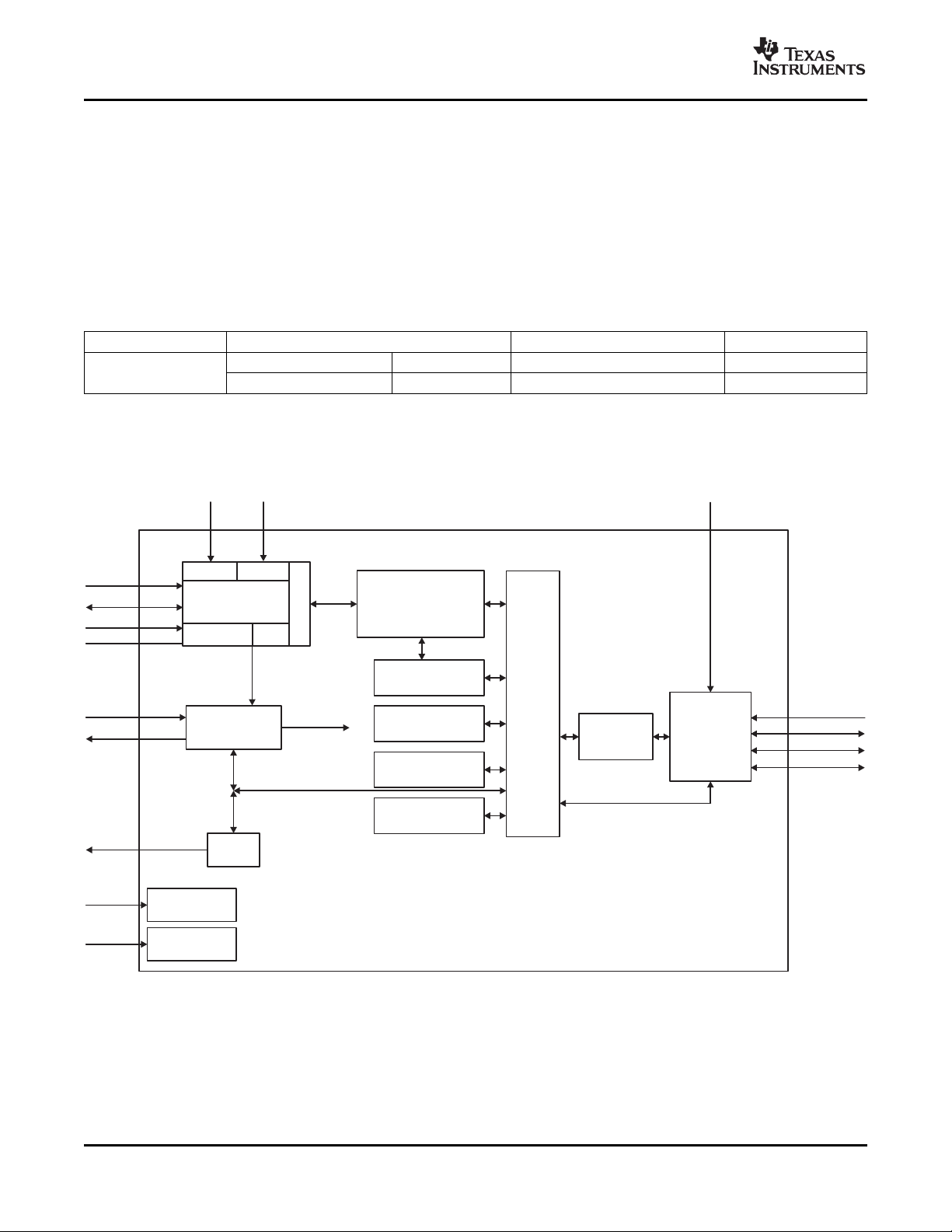
8 bit
@ 60 MHz
Central
Resource
Switch
TUSB6020
3.3 V 1.5 V
sys_clk
Digital Core
Power Distribution
IO Power
Distribution
Power/Reset/Clock
Management
(PRCM)
GPIO
CPPI 3.0
DMA
3.3 V 1.5 V
USB 2.0
PHY Macro
OTG Analog PLL
UTMI+ Le
vel 3
USB 2.0 Dual Role OTG
Controller IP Core
USB EP Buffer RAM
(16k x 8)
DMA State RAM
(DMA FIFOs)
Interrupt
Controller
XFER RAM
1.8 V
1.5 V
GPIO
5 V VBus
ID
DP/DM
XI/CLKIN
RSTn
SLEEP
3.3 V
VLYNQ_CLK
VLYNQ_CLKRUN
VLYNQ_TXD[3:0]
VLYNQ_RXD[3:0]
VLYNQ
Interface
(Ext Host Interface)
TUSB6020
USB 2.0 HIGH-SPEED ON-THE-GO DUAL-ROLE CONTROLLER
SCPS170E – JANUARY 2007 – REVISED MARCH 2008
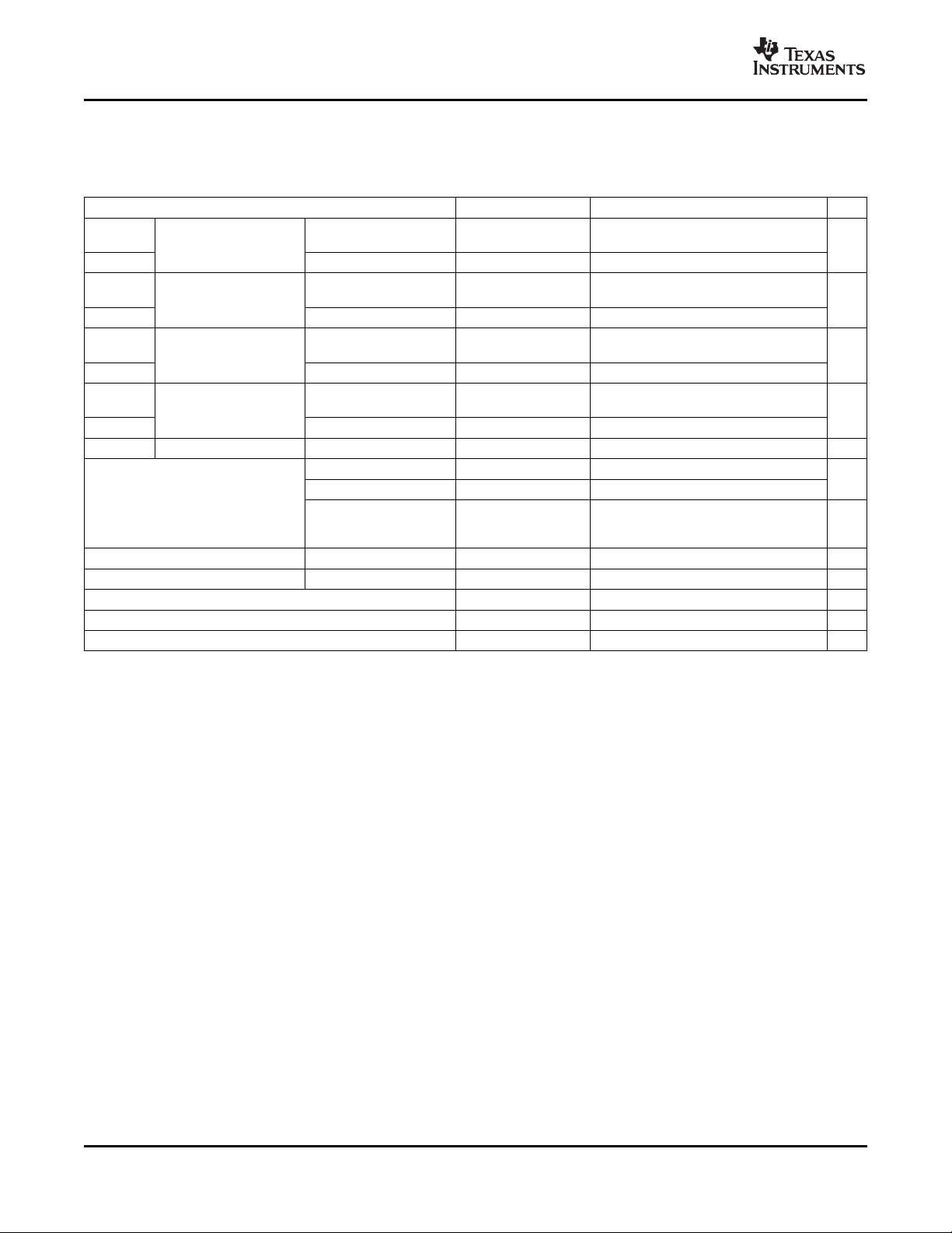
DESCRIPTION/ORDERING INFORMATION
The TUSB6020 is a USB 2.0 high-speed, on-the-go (OTG) dual-role controller designed for a seamless interface
to the VLYNQ serial interface, and is ideal for a wide range of applications. The USB OTG dual-role controller
can operate either as a function controller for a USB peripheral or as the host/peripheral in point-to-point or
multipoint communications with other functions. The integrated USB 2.0 PHY provides one-port operation at low
speed (1.5 Mbps), full speed (12 Mbps), and high speed (480 Mbps). The VLYNQ serial interface is a low pin
count, high-speed, point-to-point interface.
The device is fully compliant with Universal Serial Bus Specification Revision 2.0 and On-the-Go Supplement to
the USB Specification Revision 1.3.
ORDERING INFORMATION
(1) (2)
ORDERABLE PART NUMBER TOP-SIDE MARKING
BLOCK DIAGRAM
0 ° C to 70 ° C
T
A
MicroStar BGA™ – ZQE Reel of 360 TUSB6020ZQE PREVIEW
TQFP – PFC Tube of 96 TUSB6020PFC PREVIEW
PACKAGE
(1) Package drawings, thermal data, and symbolization are available at www.ti.com/packaging .
(2) For the most current package and ordering information, see the Package Option Addendum at the end of this document, or see the TI
website at www.ti.com .
2 Submit Documentation Feedback Copyright © 2007 – 2008, Texas Instruments Incorporated
Product Folder Link(s): TUSB6020
Page 3
www.ti.com
USB 2.0 HIGH-SPEED ON-THE-GO DUAL-ROLE CONTROLLER
SCPS170E – JANUARY 2007 – REVISED MARCH 2008
TERMINAL FUNCTIONS
TERMINAL
NAME ZQE NO. PFC NO.
1.5V_SWEN G2 18 LVCMOS O 0 Switch enable for 1.5-V LDO for VBAT/VBUS switch
3.3V_SWEN G3 19 LVCMOS O 0
CLKIN A5 71 I In
CPEN H2 22 LVCMOS O 0 5-V power distribution switch enable
DM E2 10 USB I/O – USB differential pair
DP D1 9 USB I/O – USB differential pair
GPIO0 H4 26 LVCMOS I/O In with pullup GPIO 0
GPIO1 D5 68 LVCMOS I/O In with pullup GPIO 1
GPIO2 B6 66 LVCMOS I/O In with pullup GPIO 2
GPIO3 E6 54 LVCMOS I/O In with pullup GPIO 3
GPIO4 C4 79 LVCMOS I/O In with pullup GPIO 4
GPIO5 C9 55 LVCMOS I In with pullup GPIO 5
GPIO6 F5 27 LVCMOS I/O In with pullup GPIO6 = HIGH, CLKIN is reference clock.
GPIO7 B2 2 LVCMOS I/O In with pullup
ID F2 15 USB I – information, see On-the-Go Supplement to the USB
R1 C2 5 Bias I –
RSTn H1 20 LVCMOS I In with pullup Reset active low
A8, B7, 64, 65,
B8, B9, 62, 58,
RSVD – – –
RSVD – NC – – – Reserved, should be left unconnected
SLEEP H3 24 LVCMOS O 0 OTG sleep
TEST D4 80 LVCMOS I –
VBUS F3 16 USB I –
VDD15 B3, C5, 56, 61, Supply – – Digital core power supply, 1.5 V
VDD18 Supply – – I/O power supply, 1.8 V
VDDA1P5 E3 11 Supply – – 1.5-V analog supply
VDDA3P3 C1 7 Supply – – 3.3-V analog supply
VDDCM1P5 D2 6 Supply – – 1.5-V PLL supply
VDDD1P5 F1 14 Supply – – 1.5-V digital supply
VDDS3P3 Supply – – VLYNQ supply, 3.3 V
C6, C7, 63, 60, Reserved, must be pulled low by individual pulldown
C8, D6, 57, 59, resistors. A 1-k Ω value is recommended.
D8, E7, 53, 50,
G4, J5 23, 31
G5, H5, 29, 30,
J4, F6 28, 32
A1, A9, 1, 25,
D7, J3 72, 77
A7, B5, 21, 49,
E8, J1 67, 70
F8, G6, 33, 39,
J9 44
TYPE I/O DESCRIPTION
LVCMOS 19.2-MHz system clock in. Connect directly to ground if
(1)
failsafe
RESET
STATE
Switch enable for 3.3-V CP/LDO for VBAT/VBUS
switch
not used.
GPIO 6. Input clock source select at reset.
GPIO6 = LOW, XI is reference clock.
GPIO 7. Must be pulled low for proper operation. It is
recommended to tie this signal directly to GND.
Indicates default master for OTG. For more
Specification, Revision 1.2.
High-precision external resistor used for calibration
(R1 value: 10.7 k Ω ± 1%)
Test mode. Under normal operation, this signal should
be tied directly to GND.
Charged, discharged, and monitored for OTG host
negotiation protocol and session request protocol.
External power distribution switch provides up to 500
mA.
TUSB6020
(1) Failsafe means that CLKIN can toggle when VDD18 is not present without damaging the part.
Copyright © 2007 – 2008, Texas Instruments Incorporated Submit Documentation Feedback 3
Product Folder Link(s): TUSB6020
Page 4
www.ti.com
TUSB6020
USB 2.0 HIGH-SPEED ON-THE-GO DUAL-ROLE CONTROLLER
SCPS170E – JANUARY 2007 – REVISED MARCH 2008
TERMINAL FUNCTIONS (continued)
TERMINAL
NAME ZQE NO. PFC NO.
VLYNQ_CLK F9 45 I In with pullup VLYNQ clock
VLYNQ_CRUN E9 48 3.3-V VLYNQ I/O In with pullup VLYNQ clock run
VLYNQ_RXD0 H7 38 I In with pullup VLYNQ receive data bit 0
VLYNQ_RXD1 J7 37 I In with pullup VLYNQ receive data bit 1
VLYNQ_RXD2 H6 35 I In with pullup VLYNQ receive data bit 2
VLYNQ_RXD3 J6 34 I In with pullup VLYNQ receive data bit 3
VLYNQ_TXD0 H9 40 O In with pullup VLYNQ transmit data bit 0
VLYNQ_TXD1 G9 42 O In with pullup VLYNQ transmit data bit 1
VLYNQ_TXD2 H8 43 O In with pullup VLYNQ transmit data bit 2
VLYNQ_TXD3 F7 47 O In with pullup VLYNQ transmit data bit 3
A2, A6, 17, 36,
B4, D9, 41, 46,
VSS E5, G1, 51, 52, Supply – – Ground
G7, G8, 69, 74,
J2, J8 76, 78
VSSA1P5 E1 12 Supply – – 1.5-V analog ground
VSSA3P3 E4 8 Supply – – 3.3-V analog ground
VSSCM1P5 D3 3 Supply – – 1.5-V PLL ground
VSSD1P5 F4 13 Supply – – 1.5-V digital ground
VSSREF B1 4 Supply – – Ground for the reference circuits
XI A4 73 Crystal I In Crystal input. Should be left unconnected if not used.
XO A3 75 Crystal O In Crystal output. Should be left unconnected if not used.
TYPE I/O DESCRIPTION
LVCMOS
3.3-V VLYNQ
LVCMOS
open drain
LVCMOS
3.3-V VLYNQ
LVCMOS
3.3-V VLYNQ
LVCMOS
3.3-V VLYNQ
LVCMOS
3.3-V VLYNQ
LVCMOS
3.3-V VLYNQ
LVCMOS
3.3-V VLYNQ
LVCMOS
3.3-V VLYNQ
LVCMOS
3.3-V VLYNQ
RESET
STATE
4 Submit Documentation Feedback Copyright © 2007 – 2008, Texas Instruments Incorporated
Product Folder Link(s): TUSB6020
Page 5
www.ti.com
USB 2.0 HIGH-SPEED ON-THE-GO DUAL-ROLE CONTROLLER
TUSB6020
SCPS170E – JANUARY 2007 – REVISED MARCH 2008
ABSOLUTE MAXIMUM RATINGS
(1)
over operating free-air temperature range (unless otherwise noted)
MIN MAX UNIT
V
DDA3P3
V
DDS3P3
V
DD18
V
DD15
V
DDD1P5
V
DDCM1P5
V
DDA1P5
V
I
V
I-VLYNQ
V
O
V
O-VLYNQ
V
DD
I
IK
I
OK
T
stg
3.3-V supply voltage – 0.5 4.2 V
1.8-V supply votlage – 0.5 2.1 V
1.5-V supply voltage – 0.5 2.1 V
Input voltage range V
Output voltage range V
3.3-V USB – 0.5 V
3.3-V VLYNQ – 0.5 V
3.3-V USB – 0.5 V
3.3-V VLYNQ – 0.5 V
+0.5
DDA3P3
+0.5
DDS3P3
+0.5
DDA3P3
+0.5
DDS3P3
Core supply voltage – 0.5 2.1 mA
Input clamp current ± 20 mA
Output clamp current ± 20 mA
Storage temperature range – 65 150 ° C
(1) Stresses beyond those listed under "absolute maximum ratings" may cause permanent damage to the device. These are stress ratings
only, and functional operation of the device at these or any other conditions beyond those indicated under "recommended operating
conditions" is not implied. Exposure to absolute-maximum-rated conditions for extended periods may affect device reliability.
RECOMMENDED OPERATING CONDITIONS
MIN TYP MAX UNIT
V
DDA3P3
V
DDS3P3
V
DD18
V
DD15
V
DDD1P5
V
DDCM1P5
V
DDA1P5
T
A
T
J
Supply voltage 3 3.3 3.6 V
Supply voltage Digital I/O 1.62 1.8 1.98 V
Supply voltage 1.35 1.5 1.65 V
Operating temperature 0 70 ° C
Operating junction temperature 0 ° C
OTG PHY analog
VLYNQ digital
Digital core
OTG PHY digital
OTG PHY common module
OTG PHY analog
Copyright © 2007 – 2008, Texas Instruments Incorporated Submit Documentation Feedback 5
Product Folder Link(s): TUSB6020
Page 6
www.ti.com
TUSB6020
USB 2.0 HIGH-SPEED ON-THE-GO DUAL-ROLE CONTROLLER
SCPS170E – JANUARY 2007 – REVISED MARCH 2008
DIGITAL I/O
Electrical Characteristics
TA= 0 ° C to 70 ° C, V
V
I-VLYNQ
V
I
V
O-VLYNQ
V
O
V
IH-VLYNQ
V
IH
V
IL-VLYNQ
V
IL
V
OH
V
OL
I
IH
I
IL
I
OZ
C
i
tr, t
f
Input voltage V
Output voltage V
High-level input voltage V
Low-level input voltage V
High-level output voltage LVCMOS 0.8 × V
Low-level output voltage
High-level input current LVCMOS VI= VImax ± 1 µ A
Low-level input current LVCMOS VI= VImin ± 1 µ A
Output leakage current (high Z) VI= VImax or V
Input capacitance 2 pF
Input rise/fall time 0 25 ns
= 1.8 V ± 10%, V
DD18
PARAMETER TEST CONDITIONS MIN TYP MAX UNIT
3.3-V LVCMOS
(VLYNQ only)
LVCMOS 0 V
3.3-V LVCMOS
(VLYNQ only)
LVCMOS 0 V
3.3-V LVCMOS
(VLYNQ only)
LVCMOS 0.7 × V
3.3-V LVCMOS
(VLYNQ only)
LVCMOS 0 0.3 × V
LVCMOS open drain IOL= 4 mA 0.22 × V
LVCMOS IOL= 8 mA 0.22 × V
LVCMOS
(1.5V_SWEN, IOL= 100 µ A 10 mV
3.3V_SWEN only)
DDS3P3
= 3.3 V ± 10%, V
= 0 V (unless otherwise noted)
SS
SS
0.7 × V
0 V
0 V
DDS3P3
DD18
0 0.3 × V
DD18
DDS3P3
DD18
DDS3P3
DD18
V
DDS3P3
V
DD18
DDS3P3
DD18
V
DDS3P3
V
DD18
± 20 µ A
6 Submit Documentation Feedback Copyright © 2007 – 2008, Texas Instruments Incorporated
Product Folder Link(s): TUSB6020
Page 7
www.ti.com
TUSB6020
USB 2.0 HIGH-SPEED ON-THE-GO DUAL-ROLE CONTROLLER
SCPS170E – JANUARY 2007 – REVISED MARCH 2008
SUPPLY CURRENT
Device Power Consumption
TA= 0 ° C to 70 ° C, V
V
= 3.3 V ± 10%, V
DDS3P3
PARAMETER TEST CONDITIONS UNIT
Input supply
I
DD
current
= 1.5 V ± 10%, V
DD15
DDD1P5
Power down (Idle)
No bus activity
Active (transmit/receive)
Reset
(1)
= 1.5 V ± 10%, V
(3)
(5)
= 1.8 V ± 10%, V
DD18
(2)
(4)
= 1.5 V ± 10%, V
DDA1P5
DDCM1P5
= 1.5 V ± 10%, V
= 0 V (unless otherwise noted)
SS
= 3.3 V ± 10%,
DDA3P3
IDD= 1.5 V (TOTAL) IDD= 1.8 V IDD= 3.3 V (TOTAL)
MIN TYP MAX MIN TYP MAX MIN TYP MAX
2.6 5.0 0.26 10.5 4.1 4.8
60.1 71.2 0.21 10.5 12.7 14.5
66.2 78.1 0.22 10.5 14.4 16.6
(1) Minimum, typical, and maximum current values are average values.
(2) PmIdle bit set in Device PRCM management register
(3) Normal operation with no USB connection
(4) Bulk IN and OUT on one endpoint. Packet size is 512 bytes.
(5) Device RSTn asserted
mA
Copyright © 2007 – 2008, Texas Instruments Incorporated Submit Documentation Feedback 7
Product Folder Link(s): TUSB6020
Page 8

www.ti.com
TUSB6020
USB 2.0 HIGH-SPEED ON-THE-GO DUAL-ROLE CONTROLLER
SCPS170E – JANUARY 2007 – REVISED MARCH 2008
INTEGRATED USB 2.0 TRANSCEIVER
Electrical Characteristics – V
TA= 0 ° C to 70 ° C, V
V
DDS3P3
= 3.3 V ± 10%, V
= 1.5 V ± 10%, V
DD15
DDD1P5
bus
DD18
= 1.5 V ± 10%, V
= 1.8V ± 10%, V
DDCM1P5
= 1.5 V ± 10%, V
DDA1P5
= 1.5 V ± 10%, V
= 0 V (unless otherwise noted)
SS
= 3.3 V ± 10%,
DDA3P3
PARAMETER MIN MAX UNIT
V
input impedance 360 690 k Ω
bus
V
valid comparator 4.4 4.75 V
bus
V
SRP charge pullup value 281 1950 Ω
bus
V
SRP discharge pulldown value 656 1850 Ω
bus
V
leakage current (when device is powered off) 11 µ A
bus
(1) Characterization only. Limits approved by design.
Electrical Characteristics – DP and DM
TA= 0 ° C to 70 ° C, V
V
(1) Characterization only. Limits approved by design.
= 3.3 V ± 10%, V
DDS3P3
Input Levels for Full Speed
V
DI
V
CM
Full-speed differential input threshold 0.2 V
Input (was differential) common mode range 0.8 2.5 V
Input Levels for High Speed
V
(HSSQ)
V
DI
High-speed squelch detection threshold (differential signal amplitude) 100 1520 mV
High-speed differential input threshold voltage 100 mV
Output Levels for Full Speed
V
OL
V
OH
V
O(SE1)
V
O(CRS)
Low-level output voltage 0 0.3 V
High-level output voltage (driven) 2.8 3.6 V
Output voltage on SE1 0.8 V
Output signal crossover voltage 1.3 2 V
Output Levels for High Speed
V
(HSOI)
V
(HSOH)
V
(HSOL)
V
ID(CHIRPJ)
V
ID(CHIRPK)
High-speed idle level – 10 10 mV
High-speed data signaling high 360 440 mV
High-speed data signaling low – 10 10 mV
Chirp J level (differential voltage) 700 1100 mV
Chirp K level (differential voltage) – 900 – 500 mV
Driver Characteristics (Full Speed)
t
r
t
f
t
(RFM)
Full-speed rise time 4 20 ns
Full-speed fall time 4 20 ns
Full-speed rise/fall time matching 90% 110%
Driver Characteristics (High Speed)
t
r
t
f
ro
(HSDRV)
t
(RFM)
Rise time (10%-90%) 500 ps
Fall time (10%-90%) 500 ps
Driver output resistance (serves as a high-speed termination) 40.5 49.5 Ω
Differential rise and fall time matching 90% 111.11%
Clock Timings
t
(HSDRAT)
High-speed data rate 479.76 480.24 Mb/s
= 1.5 V ± 10%, V
DD15
DDD1P5
= 1.5 V ± 10%, V
DD18
PARAMETER MIN MAX UNIT
= 1.8 V ± 10%, V
DDCM1P5
= 1.5 V ± 10%, V
DDA1P5
= 1.5 V ± 10%, V
= 0 V (unless otherwise noted)
SS
= 3.3 V ± 10%,
DDA3P3
(1)
(1)
8 Submit Documentation Feedback Copyright © 2007 – 2008, Texas Instruments Incorporated
Product Folder Link(s): TUSB6020
Page 9

www.ti.com
TUSB6020
USB 2.0 HIGH-SPEED ON-THE-GO DUAL-ROLE CONTROLLER
SCPS170E – JANUARY 2007 – REVISED MARCH 2008
Electrical Characteristics – DP and DM (continued)
TA= 0 ° C to 70 ° C, V
V
= 3.3 V ± 10%, V
DDS3P3
Single-Ended Receiver
V
IT+
V
IT –
V
hys
Positive-going input threshold voltage 2.0 V
Negative-going input threshold voltage 0.8 V
Hysteresis voltage 200 500 mV
Input Leakage
DP Measurement taken with pulldown disabled and device in idle mode 10 nA
DM Measurement taken with pulldown disabled and device in idle mode 10 nA
= 1.5 V ± 10%, V
DD15
DDD1P5
= 1.5 V ± 10%, V
DD18
PARAMETER MIN MAX UNIT
= 1.8 V ± 10%, V
DDCM1P5
= 1.5 V ± 10%, V
DDA1P5
= 1.5 V ± 10%, V
= 0 V (unless otherwise noted)
SS
= 3.3 V ± 10%,
DDA3P3
Copyright © 2007 – 2008, Texas Instruments Incorporated Submit Documentation Feedback 9
Product Folder Link(s): TUSB6020
Page 10

www.ti.com
TUSB6020
USB 2.0 HIGH-SPEED ON-THE-GO DUAL-ROLE CONTROLLER
SCPS170E – JANUARY 2007 – REVISED MARCH 2008
VLYNQ INTERFACE
Electrical Characteristics
TA= 0 ° C to 70 ° C, V
V
= 3.3 V ± 10%, V
DDS3P3
PARAMETER TEST CONDITIONS MIN TYP MAX UNIT
I
Low-level input current LVCMOS 8 mA
OL
I
High-level input current LVCMOS – 8 mA
OH
V
High-level output voltage LVCMOS V
OH
V
Low-level output voltage LVCMOS V
OL
V
Hysteresis LVCMOS V
hys
I
High-level input current Receiver only V
IH
I
Low-level input current Receiver only V
IL
Output leakage current
I
OZ
(Hi-Z)
Switching Characteristics
TA= 0 ° C to 70 ° C, V
V
= 3.3 V ± 10%, V
DDS3P3
Driver Characteristics
Rise time
t
r
(between 10% and 90% swing of 3.3 V)
Fall time
t
f
(between 90% and 10% swing of 3.3 V)
= 1.5 V ± 10%, V
DD15
DDD1P5
= 1.5 V ± 10%, V
= 1.8 V ± 10%, V
DD18
DDCM1P5
DDA1P5
= 1.5 V ± 10%, V
IO= – 100 µ A V
IO= I
OH
= 1.5 V ± 10%, V
= 0 V (unless otherwise noted)
SS
– 0.2
DDS3P3
0.8 × V
DDSS3P3
= 3.3 V ± 10%,
DDA3P3
IO= 100 µ A 0.2
IO= I
OL
= V
I-VLYNQ
I-VLYNQ
I-VLYNQ
IH-VLYNQ
= V
= V
max ± 1 µ A
I-VLYNQ
min ± 1 µ A
I-VLYNQ
0.13 × V
DDSS3P3
Driver only Driver disabled ± 20 µ A
= 1.5 V ± 10%, V
DD15
DDD1P5
= 1.5 V ± 10%, V
= 1.8 V ± 10%, V
DD18
= 1.5 V ± 10%, V
DDA1P5
DDCM1P5
= 1.5 V ± 10%, V
= 0 V (unless otherwise noted)
SS
= 3.3 V ± 10%,
DDA3P3
PARAMETER TEST CONDITIONS TYP UNIT
Load: CL= 10 pF 1.68
Load: CL= 50 pF 6.56 ns
Load: CL= 125 pF 15.78
Load: CL= 5 pF 2.09
Load: CL= 5 pF 8.19 ns
Load: CL= 15 pF 19.75
0.22 ×
V
S3P3
DDS
V
10 Submit Documentation Feedback Copyright © 2007 – 2008, Texas Instruments Incorporated
Product Folder Link(s): TUSB6020
Page 11

www.ti.com
TUSB6020
USB 2.0 HIGH-SPEED ON-THE-GO DUAL-ROLE CONTROLLER
SCPS170E – JANUARY 2007 – REVISED MARCH 2008
APPLICATION INFORMATION
Power-On Reset
The system reset function ensures an orderly start-up sequence for the TUSB6020. There is one active-low
external system reset (RSTn) input . The reset initializes the power/reset/clock manager (PRCM) module, which
in turn generates all the internal resets to initialize USB 2.0 OTG PHY macro and synchronous logic in the core.
While reset is asserted (active low), dual functional pins are sampled to determine device configuration after
reset. Since the TUSB6020 relies on dual function pins to configure the device during reset, the reset must be
sufficiently long for (external) marginal pullup/pulldown to achieve the intended levels. Reset pulse duration
should be at least three times actual RC constant time (with typical 22 k Ω marginal pull-up resistor with 50-pF
load, reset pulse should be at least 3.3 µ s). All functional pins remain in the same state even after RSTn is
deasserted and stay in that state until the internal core reset is cleared. The internal core reset is held for 16
system clock cycles following the low-to-high RSTn transition. Upon power-on reset, the system reference clock
source and the active external host interface must be determined for proper device initialization.
Table 1. Dual-Function GPIOs
EXTERNAL PIN FUNCTION DESCRIPTION
GPIO6 Reference clock source select 0 – XI (24 MHz)
GPIO7 External host interface select 0 – VLYNQ host interface
Determines the system reference clock source:
1 – CLKIN (19.2 MHz)Dual
Determines the external host interface type:
1 – Reserved
The TUSB6020 uses dual-mode pins to determine initial setup. Dual-function pins are latched during the reset.
After the reset, these terminals assumes the normal functionality. Figure 1 shows the power-up sequence.
Upon exiting reset, the USB 2.0 OTG PHY is not in the suspend state and the clocks are enabled and free
running. The USB 2.0 HS OTG dual role controller core powers up without a session enabled, thus the state
machines are in the idle state. After reset is deasserted, the TUSB6020 sends an interrupt to the external host to
indicate that it is ready to be programmed. The host reads registers and decides how to proceed based on the
device ’ s current status.
Device Power States
The TUSB6020 has three device states typically entered under normal operation:
• RESET
• IDLE
• NORMAL (ACTIVE)
RESET State
The device is in the RESET state when the RSTn input signal is driven low. In RESET state:
• All output ports are tri-stated or initialized to inactive state.
• All bidirectional ports are configured as inputs.
• All registers are set to their reset value.
• PHY macro is enabled and its reference clock output is active.
The TUSB6020 always enters the RESET state asynchronously, but exits the state synchronously. System reset
deassertion is always synchronized with active system clock. Upon asserted system reset, the device requires an
active system clock to exit the RESET state.
Copyright © 2007 – 2008, Texas Instruments Incorporated Submit Documentation Feedback 11
Product Folder Link(s): TUSB6020
Page 12

www.ti.com
TUSB6020
USB 2.0 HIGH-SPEED ON-THE-GO DUAL-ROLE CONTROLLER
SCPS170E – JANUARY 2007 – REVISED MARCH 2008
IDLE State
The TUSB6020 enters IDLE state when external host sets DevIdle bit in the device power management register.
The external host may decide to place the device into IDLE state if:
• No USB cable is attached.
• The type-B connector is attached, but the type-A device did not charge V
• The type-A connector is attached, but the external host may decide to wait for an SRP request from the
type-B device.
In IDLE state:
• All output signals are driven to state with minimum I/O current leakage (pullup/pulldowns are controllable
through Pullup/Pulldown Control registers).
• All controllable bidirectional pins are placed into minimum current leakage state.
• All registers and memories retain the content and any read/write registers access is disabled.
• All clock sources are disabled.
• PHY macro is suspended:
1. Low-power V
sense comparator is enabled and all regular V
BUS
BUS
current consumption.
2. ID detection circuitry is enabled.
3. Remaining analog circuitry is disabled.
In IDLE state, the device asserts the SLEEP output pin to the companion power-management device to place it
into low-power/sleep mode if the PmIdle and DevIdle bits are set in the PRCM power management register. The
power-management device can be put into the sleep state only if the device is placed in IDLE state (DevIdle bit
set).
If the application requires the companion power-management device to remain in NORMAL state, the PmIdle bit
will not be set, while the DevIdle bit can be set to place the device into the idle state. TUSB6020 stays in the
IDLE state until a valid wake-up event occurs and transitions into NORMAL (ACTIVE) State. If system reset is
asserted (RSTn), the device transitions to RESET state.
.
BUS
comparators are disabled to minimize
NORMAL (ACTIVE) State
A transition to NORMAL state is required for normal device operation. All circuitry is enabled. In NORMAL state:
• All I/Os are enabled.
• All registers and memories are accessible.
• Clock source are enabled.
• PHY macro is enabled.
• Session end V
• V
detection circuitry is enabled.
BUS
BUS
detect circuitry is enabled.
• ID detection circuitry is enabled.
The external host enables IDpullup and the V
sense comparator. It reads the Device Status register to confirm
BUS
the USB cable connection.
• If no USB cable is attached, IDpullup should be high and V
• If the type-B USB connector is attached, IDpullup should be high. The V
type-A device on the other side of the cable is charging V
• If the type-A USB connector is attached, IDpullup should be low and V
decides when to charge V
.
BUS
should be low.
BUS
status depends on whether the
.
BUS
BUS
should be low. The external host
BUS
12 Submit Documentation Feedback Copyright © 2007 – 2008, Texas Instruments Incorporated
Product Folder Link(s): TUSB6020
Page 13

www.ti.com
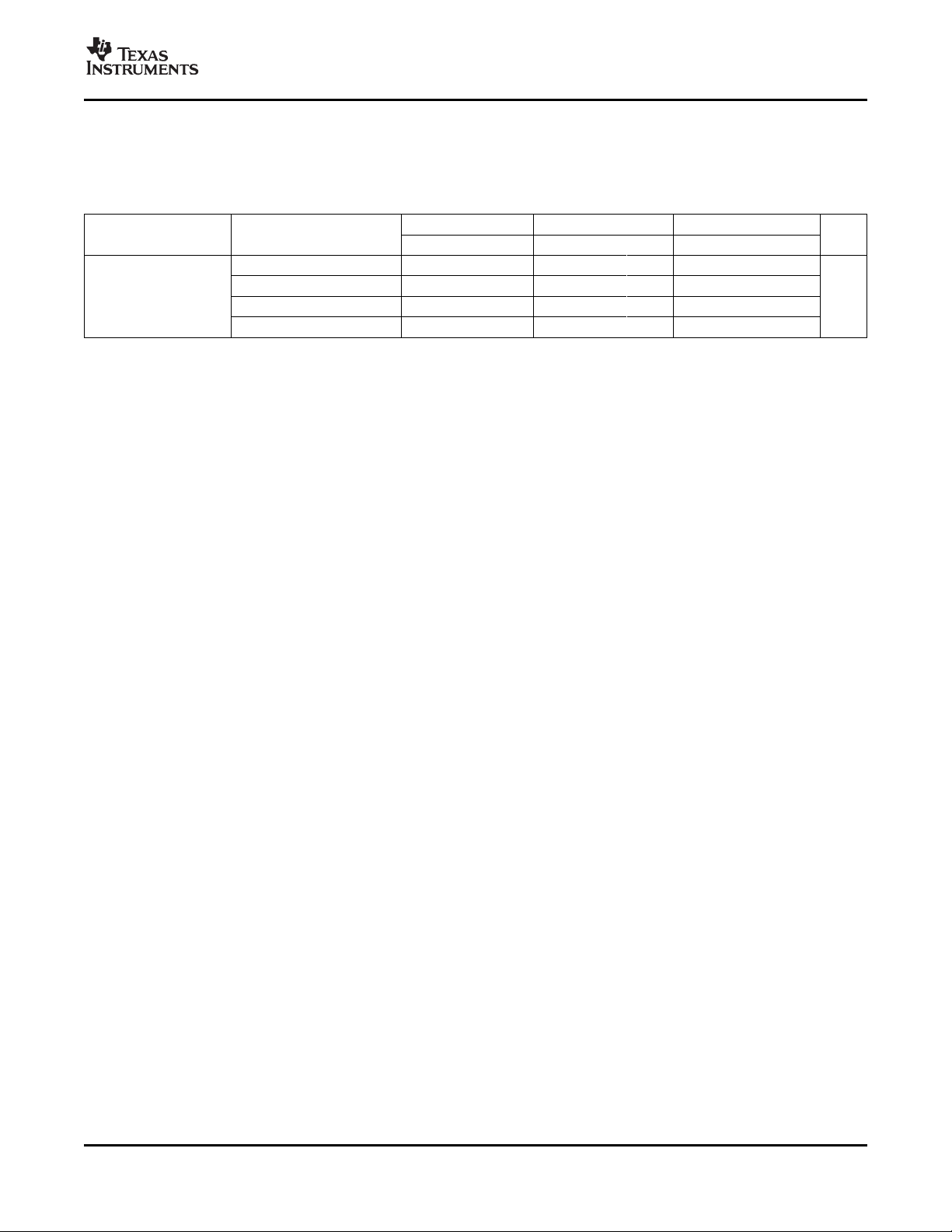
Power-Sequencing Guidelines
V /V (5 V)
BAT IN
Ext. Pwr. Mgmt (1.8 V)
TUSB6020: CPEN
V Power: En1 (5 V)
BUS
3.3 V, 1.5 V LDO: Pgood
TUSB6020: RSTn
LDO Voltage Regulator (1.5 V)
LDO Voltage Regulator (3.3 V)
TUSB6020: IO Interface Status
TUSB6020: GPIO7
(Mode Select)
TUSB6020: GPIO6
(Reference Clock Select)
Signal state cannot be ensured.
Signal state is stable and valid.
NOTE: Host mode and reference clock source selection is latched on RSTn rising edge. No external components are required to select normal
mode and CLKIN as a reference clock source.
IOINTERFACEISNOT INITIALIZED
IOINTERFACEISINITIALIZED
GPIO7 is tied to ground externally for normal device operation
Pulled up by TUSB6020 GPIO6 internal pullup resistor (CLKIN is selected)
Pulled high by TUSB6020
internal pullup
NOTE: CPEN is used to drive the enable of the V power switch. The TUSB6020 does not power up with CPEN asserted. CPEN is
asserted when TUSB6020 is recognized as an A device.
BUS
TUSB6020
USB 2.0 HIGH-SPEED ON-THE-GO DUAL-ROLE CONTROLLER
SCPS170E – JANUARY 2007 – REVISED MARCH 2008
Crystal Requirements
Frequency
The required frequency of oscillation for the crystal can be 19.200 or 24.000 MHz.
Frequency Tolerance
Frequency tolerance is the maximum allowable deviation from the nominal crystal frequency at a specified
temperature, usually 25 ° C. The recommended frequency tolerance of the crystal over the manufacturing process
is ± 50 ppm. The maximum acceptable frequency tolerance of the crystal over the manufacturing process is
± 100 ppm.
Nominal clock frequency 19.200 (CLKIN), 24.000 (XI)
Frequency accuracy ± 100 ppm
Maximum rise/fall time 5 ns (10% to 90%)
Voltage level 1.8 V
Input clock type Square wave, Sine wave
Duty cycle 40% to 60%
Input capacitance loading 4 pF
Jitter
Figure 1. System Power-Up Sequence
Table 2. INPUT CLOCK REQUIREMENTS
PARAMETER VALUE
– 95 dBc at 1 MHz
– 120 dBc at 100 MHz
Copyright © 2007 – 2008, Texas Instruments Incorporated Submit Documentation Feedback 13
Product Folder Link(s): TUSB6020
Page 14

www.ti.com
MicroStar BGA™/ Junior™
Recommended Lead Free Reflow Profile
In the case of Sn/Ag/Cu solder paste
MicroStar
Reflow temperature is defined at package top.
Time
Peak temperature
260°C max
30 – 60 s
90 ± 30 s
1–5 sec
°C/
(°C)
260
235
225
200
150
TUSB6020
USB 2.0 HIGH-SPEED ON-THE-GO DUAL-ROLE CONTROLLER
SCPS170E – JANUARY 2007 – REVISED MARCH 2008
NOTE:
The total system frequency tolerance from the crystal, load capacitors, capacitive load
of the board, capacitive load of the device pins, variation over temperature, variation
with age, and circuitry of the PHY must be less than ± 500 ppm. Consequently, the
individual tolerance for the crystal must be ≤ ± 100 ppm.
Load Capacitance
The oscillator of the USB device may have difficulty driving a large load capacitance, so crystals that specify
large load capacitances should be avoided. For more information on crystal requirements, see Selection and
Specification of Crystals for Texas Instruments USB 2.0 Devices (literature number SLLA122).
Mechanical Characteristics
The TUSB6020 controller uses an 80-pin MicroStar BGA™ package. The lead-free solder ball composition is
Sn/Ag1.2Cu0.5 (proportions by weight). The substrate plating on the die side where the die bonds to is NiAu.
The substrate finish on the bottom side where the solder balls attach to is bare Cu.
Reflow Conditions - ZQE Package
Figure 2. Reflow Conditions
The TUSB6020 controller can also use an 80-pin PFC (TQFP) package.
14 Submit Documentation Feedback Copyright © 2007 – 2008, Texas Instruments Incorporated
Product Folder Link(s): TUSB6020
Page 15

PACKAGE OPTION ADDENDUM
www.ti.com
7-Oct-2010
PACKAGING INFORMATION
Orderable Device
TUSB6020PFC ACTIVE TQFP PFC 80 96 Green (RoHS
TUSB6020PFCG4 ACTIVE TQFP PFC 80 96 Green (RoHS
TUSB6020PFCR ACTIVE TQFP PFC 80 1000 Green (RoHS
TUSB6020PFCRG4 ACTIVE TQFP PFC 80 1000 Green (RoHS
TUSB6020ZQE ACTIVE BGA
TUSB6020ZQER ACTIVE BGA
(1)
The marketing status values are defined as follows:
ACTIVE: Product device recommended for new designs.
LIFEBUY: TI has announced that the device will be discontinued, and a lifetime-buy period is in effect.
NRND: Not recommended for new designs. Device is in production to support existing customers, but TI does not recommend using this part in a new design.
PREVIEW: Device has been announced but is not in production. Samples may or may not be available.
OBSOLETE: TI has discontinued the production of the device.
Status
(1)
Package Type Package
MICROSTAR
JUNIOR
MICROSTAR
JUNIOR
Drawing
Pins Package Qty
ZQE 80 360 Green (RoHS
ZQE 80 2500 Green (RoHS
Eco Plan
& no Sb/Br)
& no Sb/Br)
& no Sb/Br)
& no Sb/Br)
& no Sb/Br)
& no Sb/Br)
(2)
Lead/
Ball Finish
CU NIPDAU Level-4-260C-72 HR Request Free Samples
CU NIPDAU Level-4-260C-72 HR Request Free Samples
CU NIPDAU Level-4-260C-72 HR Purchase Samples
CU NIPDAU Level-4-260C-72 HR Purchase Samples
SNAGCU Level-3-260C-168 HR Request Free Samples
SNAGCU Level-3-260C-168 HR Purchase Samples
MSL Peak Temp
(3)
Samples
(Requires Login)
(2)
Eco Plan - The planned eco-friendly classification: Pb-Free (RoHS), Pb-Free (RoHS Exempt), or Green (RoHS & no Sb/Br) - please check http://www.ti.com/productcontent for the latest availability
information and additional product content details.
TBD: The Pb-Free/Green conversion plan has not been defined.
Pb-Free (RoHS): TI's terms "Lead-Free" or "Pb-Free" mean semiconductor products that are compatible with the current RoHS requirements for all 6 substances, including the requirement that
lead not exceed 0.1% by weight in homogeneous materials. Where designed to be soldered at high temperatures, TI Pb-Free products are suitable for use in specified lead-free processes.
Pb-Free (RoHS Exempt): This component has a RoHS exemption for either 1) lead-based flip-chip solder bumps used between the die and package, or 2) lead-based die adhesive used between
the die and leadframe. The component is otherwise considered Pb-Free (RoHS compatible) as defined above.
Green (RoHS & no Sb/Br): TI defines "Green" to mean Pb-Free (RoHS compatible), and free of Bromine (Br) and Antimony (Sb) based flame retardants (Br or Sb do not exceed 0.1% by weight
in homogeneous material)
(3)
MSL, Peak Temp. -- The Moisture Sensitivity Level rating according to the JEDEC industry standard classifications, and peak solder temperature.
Important Information and Disclaimer:The information provided on this page represents TI's knowledge and belief as of the date that it is provided. TI bases its knowledge and belief on information
provided by third parties, and makes no representation or warranty as to the accuracy of such information. Efforts are underway to better integrate information from third parties. TI has taken and
Addendum-Page 1
Page 16

PACKAGE OPTION ADDENDUM
www.ti.com
continues to take reasonable steps to provide representative and accurate information but may not have conducted destructive testing or chemical analysis on incoming materials and chemicals.
TI and TI suppliers consider certain information to be proprietary, and thus CAS numbers and other limited information may not be available for release.
7-Oct-2010
In no event shall TI's liability arising out of such information exceed the total purchase price of the TI part(s) at issue in this document sold by TI to Customer on an annual basis.
Addendum-Page 2
Page 17

PACKAGE MATERIALS INFORMATION
www.ti.com 21-Feb-2011
TAPE AND REEL INFORMATION
*All dimensions are nominal
Device Package
TUSB6020ZQER BGA MI
Type
CROSTA
R JUNI
OR
Package
Drawing
Pins SPQ Reel
Diameter
(mm)
ZQE 80 2500 330.0 12.4 5.3 5.3 1.5 8.0 12.0 Q1
Reel
Width
W1 (mm)
A0
(mm)B0(mm)K0(mm)P1(mm)W(mm)
Pin1
Quadrant
Pack Materials-Page 1
Page 18

PACKAGE MATERIALS INFORMATION
www.ti.com 21-Feb-2011
*All dimensions are nominal
Device Package Type Package Drawing Pins SPQ Length (mm) Width (mm) Height (mm)
TUSB6020ZQER BGA MICROSTAR
JUNIOR
ZQE 80 2500 340.5 333.0 20.6
Pack Materials-Page 2
Page 19

Page 20

MECHANICAL DATA
MTQF009A – OCTOBER 1994 – REVISED DECEMBER 1996
PFC (S-PQFP-G80) PLASTIC QUAD FLATPACK
61
80
1,05
0,95
0,50
60
0,27
0,17
41
1
9,50 TYP
12,20
SQ
11,80
14,20
SQ
13,80
20
0,08
21
40
M
0,13 NOM
Gage Plane
0,25
0,05 MIN
0,75
0,45
0°–7°
1,20 MAX
NOTES: A. All linear dimensions are in millimeters.
B. This drawing is subject to change without notice.
C. Falls within JEDEC MS-026
Seating Plane
0,08
4073177/B 11/96
POST OFFICE BOX 655303 • DALLAS, TEXAS 75265
Page 21

IMPORTANT NOTICE
Texas Instruments Incorporated and its subsidiaries (TI) reserve the right to make corrections, modifications, enhancements, improvements,
and other changes to its products and services at any time and to discontinue any product or service without notice. Customers should
obtain the latest relevant information before placing orders and should verify that such information is current and complete. All products are
sold subject to TI’s terms and conditions of sale supplied at the time of order acknowledgment.
TI warrants performance of its hardware products to the specifications applicable at the time of sale in accordance with TI’s standard
warranty. Testing and other quality control techniques are used to the extent TI deems necessary to support this warranty. Except where
mandated by government requirements, testing of all parameters of each product is not necessarily performed.
TI assumes no liability for applications assistance or customer product design. Customers are responsible for their products and
applications using TI components. To minimize the risks associated with customer products and applications, customers should provide
adequate design and operating safeguards.
TI does not warrant or represent that any license, either express or implied, is granted under any TI patent right, copyright, mask work right,
or other TI intellectual property right relating to any combination, machine, or process in which TI products or services are used. Information
published by TI regarding third-party products or services does not constitute a license from TI to use such products or services or a
warranty or endorsement thereof. Use of such information may require a license from a third party under the patents or other intellectual
property of the third party, or a license from TI under the patents or other intellectual property of TI.
Reproduction of TI information in TI data books or data sheets is permissible only if reproduction is without alteration and is accompanied
by all associated warranties, conditions, limitations, and notices. Reproduction of this information with alteration is an unfair and deceptive
business practice. TI is not responsible or liable for such altered documentation. Information of third parties may be subject to additional
restrictions.
Resale of TI products or services with statements different from or beyond the parameters stated by TI for that product or service voids all
express and any implied warranties for the associated TI product or service and is an unfair and deceptive business practice. TI is not
responsible or liable for any such statements.
TI products are not authorized for use in safety-critical applications (such as life support) where a failure of the TI product would reasonably
be expected to cause severe personal injury or death, unless officers of the parties have executed an agreement specifically governing
such use. Buyers represent that they have all necessary expertise in the safety and regulatory ramifications of their applications, and
acknowledge and agree that they are solely responsible for all legal, regulatory and safety-related requirements concerning their products
and any use of TI products in such safety-critical applications, notwithstanding any applications-related information or support that may be
provided by TI. Further, Buyers must fully indemnify TI and its representatives against any damages arising out of the use of TI products in
such safety-critical applications.
TI products are neither designed nor intended for use in military/aerospace applications or environments unless the TI products are
specifically designated by TI as military-grade or "enhanced plastic." Only products designated by TI as military-grade meet military
specifications. Buyers acknowledge and agree that any such use of TI products which TI has not designated as military-grade is solely at
the Buyer's risk, and that they are solely responsible for compliance with all legal and regulatory requirements in connection with such use.
TI products are neither designed nor intended for use in automotive applications or environments unless the specific TI products are
designated by TI as compliant with ISO/TS 16949 requirements. Buyers acknowledge and agree that, if they use any non-designated
products in automotive applications, TI will not be responsible for any failure to meet such requirements.
Following are URLs where you can obtain information on other Texas Instruments products and application solutions:
Products Applications
Audio www.ti.com/audio Communications and Telecom www.ti.com/communications
Amplifiers amplifier.ti.com Computers and Peripherals www.ti.com/computers
Data Converters dataconverter.ti.com Consumer Electronics www.ti.com/consumer-apps
DLP® Products www.dlp.com Energy and Lighting www.ti.com/energy
DSP dsp.ti.com Industrial www.ti.com/industrial
Clocks and Timers www.ti.com/clocks Medical www.ti.com/medical
Interface interface.ti.com Security www.ti.com/security
Logic logic.ti.com Space, Avionics and Defense www.ti.com/space-avionics-defense
Power Mgmt power.ti.com Transportation and www.ti.com/automotive
Microcontrollers microcontroller.ti.com Video and Imaging www.ti.com/video
RFID www.ti-rfid.com Wireless www.ti.com/wireless-apps
RF/IF and ZigBee® Solutions www.ti.com/lprf
TI E2E Community Home Page e2e.ti.com
Automotive
Mailing Address: Texas Instruments, Post Office Box 655303, Dallas, Texas 75265
Copyright © 2011, Texas Instruments Incorporated
 Loading...