

Page 1

TUSB3410 GeneralĆPurpose
Input/Output Evaluation
Board
User’s Guide
September 2002 Universal Serial Bus Products
SLLU041
Page 2

IMPORTANT NOTICE
Texas Instruments Incorporated and its subsidiaries (TI) reserve the right to make corrections, modifications,
enhancements, improvements, and other changes to its products and services at any time and to discontinue
any product or service without notice. Customers should obtain the latest relevant information before placing
orders and should verify that such information is current and complete. All products are sold subject to TI’s terms
and conditions of sale supplied at the time of order acknowledgment.
TI warrants performance of its hardware products to the specifications applicable at the time of sale in
accordance with TI’s standard warranty . Testing and other quality control techniques are used to the extent TI
deems necessary to support this warranty . Except where mandated by government requirements, testing of all
parameters of each product is not necessarily performed.
TI assumes no liability for applications assistance or customer product design. Customers are responsible for
their products and applications using TI components. T o minimize the risks associated with customer products
and applications, customers should provide adequate design and operating safeguards.
TI does not warrant or represent that any license, either express or implied, is granted under any TI patent right,
copyright, mask work right, or other TI intellectual property right relating to any combination, machine, or process
in which TI products or services are used. Information published by TI regarding third-party products or services
does not constitute a license from TI to use such products or services or a warranty or endorsement thereof.
Use of such information may require a license from a third party under the patents or other intellectual property
of the third party , or a license from TI under the patents or other intellectual property of TI.
Reproduction of information in TI data books or data sheets is permissible only if reproduction is without
alteration and is accompanied by all associated warranties, conditions, limitations, and notices. Reproduction
of this information with alteration is an unfair and deceptive business practice. TI is not responsible or liable for
such altered documentation.
Resale of TI products or services with statements different from or beyond the parameters stated by TI for that
product or service voids all express and any implied warranties for the associated TI product or service and
is an unfair and deceptive business practice. TI is not responsible or liable for any such statements.
Mailing Address:
Texas Instruments
Post Office Box 655303
Dallas, Texas 75265
Copyright 2002, Texas Instruments Incorporated
Page 3

EVM IMPORTANT NOTICE
Texas Instruments (TI) provides the enclosed product(s) under the following conditions:
This evaluation kit being sold by TI is intended for use for ENGINEERING DEVELOPMENT OR EV ALUA TION
PURPOSES ONL Y and is not considered by TI to be fit for commercial use. As such, the goods being provided
may not be complete in terms of required design-, marketing-, and/or manufacturing-related protective
considerations, including product safety measures typically found in the end product incorporating the goods.
As a prototype, this product does not fall within the scope of the European Union directive on electromagnetic
compatibility and therefore may not meet the technical requirements of the directive.
Should this evaluation kit not meet the specifications indicated in the EVM User’s Guide, the kit may be returned
within 30 days from the date of delivery for a full refund. THE FOREGOING WARRANTY IS THE EXCLUSIVE
WARRANTY MADE BY SELLER TO BUYER AND IS IN LIEU OF ALL OTHER WARRANTIES, EXPRESSED,
IMPLIED, OR ST ATUT ORY, INCLUDING ANY W ARRANTY OF MERCHANTABILITY OR FITNESS FOR ANY
PARTICULAR PURPOSE.
The user assumes all responsibility and liability for proper and safe handling of the goods. Further, the user
indemnifies TI from all claims arising from the handling or use of the goods. Please be aware that the products
received may not be regulatory compliant or agency certified (FCC, UL, CE, etc.). Due to the open construction
of the product, it is the user’s responsibility to take any and all appropriate precautions with regard to electrostatic
discharge.
EXCEPT TO THE EXTENT OF THE INDEMNITY SET FORTH ABOVE, NEITHER P ARTY SHALL BE LIABLE
TO THE OTHER FOR ANY INDIRECT, SPECIAL, INCIDENTAL, OR CONSEQUENTIAL DAMAGES.
TI currently deals with a variety of customers for products, and therefore our arrangement with the user is not
exclusive.
TI assumes no liability for applications assistance, customer product design, software performance, or
infringement of patents or services described herein.
Please read the EVM User’s Guide and, specifically, the EVM Warnings and Restrictions notice in the EVM
User’s Guide prior to handling the product. This notice contains important safety information about temperatures
and voltages. For further safety concerns, please contact the TI application engineer.
Persons handling the product must have electronics training and observe good laboratory practice standards.
No license is granted under any patent right or other intellectual property right of TI covering or relating to any
machine, process, or combination in which such TI products or services might be or are used.
Mailing Address:
Texas Instruments
Post Office Box 655303
Dallas, Texas 75265
Copyright 2002, Texas Instruments Incorporated
Page 4

EVM WARNINGS AND RESTRICTIONS
It is important to operate this EVM within the input voltage range of 4.75 V and the output
voltage range of 4.75 V and 5.25 V.
Exceeding the specified input range may cause unexpected operation and/or irreversible
damage to the EVM. If there are questions concerning the input range, please contact a TI
field representative prior to connecting the input power.
Applying loads outside of the specified output range may result in unintended operation and/or
possible permanent damage to the EVM. Please consult the EVM User’s Guide prior to
connecting any load to the EVM output. If there is uncertainty as to the load specification,
please contact a TI field representative.
During normal operation, some circuit components may have case temperatures greater than
50°C. The EVM is designed to operate properly with certain components above 60°C as long
as the input and output ranges are maintained. These components include but are not limited
to linear regulators, switching transistors, pass transistors, and current sense resistors. These
types of devices can be identified using the EVM schematic located in the EVM User’s Guide.
When placing measurement probes near these devices during operation, please be aware
that these devices may be very warm to the touch.
Mailing Address:
Texas Instruments
Post Office Box 655303
Dallas, Texas 75265
Copyright 2002, Texas Instruments Incorporated
Page 5

About This Manual
Related Documentation From Texas Instruments
Preface
Read This First
This user’s guide describes the setup and operation of the TUSB3410 general-
purpose input/output evaluation board. Familiarity with the universal serial bus
(USB) protocol and common lab testing equipment is required, and is assumed throughout this user’s guide.
How to Use This Manual
This document contains the following chapters:
- Chapter 1—Required Hardware and Software
- Chapter 2—EVM Operation
- Chapter 3—Bill of Materials and EVM Layouts
- Appendix A—TUSB3410 GPIO EVM Schematic Diagram
Related Documentation From Texas Instruments
TUSB3410 USB to Serial Port Controller data manual Literature No. SLLS519
FCC Warning
This equipment is intended for use in a laboratory test environment only . It generates, uses, and can radiate radio frequency energy and has not been tested
for compliance with the limits of computing devices pursuant to subpart J of
part 15 of FCC rules, which are designed to provide reasonable protection
against radio frequency interference. Operation of this equipment in other environments may cause interference with radio communications, in which case
the user at his own expense will be required to take whatever measures may
be required to correct this interference.
v
Page 6

vi
Page 7

Contents
Contents
1 Required Hardware and Software 1-1. . . . . . . . . . . . . . . . . . . . . . . . . . . . . . . . . . . . . . . . . . . . . . . . .
1.1 Hardware Items 1-2. . . . . . . . . . . . . . . . . . . . . . . . . . . . . . . . . . . . . . . . . . . . . . . . . . . . . . . . . . . .
1.2 Hardware Overview 1-3. . . . . . . . . . . . . . . . . . . . . . . . . . . . . . . . . . . . . . . . . . . . . . . . . . . . . . . . .
2 EVM Operation 2-1. . . . . . . . . . . . . . . . . . . . . . . . . . . . . . . . . . . . . . . . . . . . . . . . . . . . . . . . . . . . . . . . . .
2.1 TUSB3410 EVM Setup 2-2. . . . . . . . . . . . . . . . . . . . . . . . . . . . . . . . . . . . . . . . . . . . . . . . . . . . . .
2.2 Interfaces and USB Ports 2-2. . . . . . . . . . . . . . . . . . . . . . . . . . . . . . . . . . . . . . . . . . . . . . . . . . . .
2.3 Power Supply 2-2. . . . . . . . . . . . . . . . . . . . . . . . . . . . . . . . . . . . . . . . . . . . . . . . . . . . . . . . . . . . . .
2.4 Buttons 2-2. . . . . . . . . . . . . . . . . . . . . . . . . . . . . . . . . . . . . . . . . . . . . . . . . . . . . . . . . . . . . . . . . . . .
2.5 Light Emitting Diodes (LEDs) 2-2. . . . . . . . . . . . . . . . . . . . . . . . . . . . . . . . . . . . . . . . . . . . . . . . .
2.6 Jumpers 2-3. . . . . . . . . . . . . . . . . . . . . . . . . . . . . . . . . . . . . . . . . . . . . . . . . . . . . . . . . . . . . . . . . . .
2.7 EEPROM 2-3. . . . . . . . . . . . . . . . . . . . . . . . . . . . . . . . . . . . . . . . . . . . . . . . . . . . . . . . . . . . . . . . . .
3 Bill of Materials and EVM Layouts 3-1. . . . . . . . . . . . . . . . . . . . . . . . . . . . . . . . . . . . . . . . . . . . . . . .
3.1 Bill of Materials 3-2. . . . . . . . . . . . . . . . . . . . . . . . . . . . . . . . . . . . . . . . . . . . . . . . . . . . . . . . . . . . .
3.2 EVM Layouts 3-3. . . . . . . . . . . . . . . . . . . . . . . . . . . . . . . . . . . . . . . . . . . . . . . . . . . . . . . . . . . . . . .
4 TUSB3410 GPIO EVM Schematic Diagram A-1. . . . . . . . . . . . . . . . . . . . . . . . . . . . . . . . . . . . . . . . .
Figures
1–1 TUSB3410 Evaluation Hardware 1-2. . . . . . . . . . . . . . . . . . . . . . . . . . . . . . . . . . . . . . . . . . . . . . . .
1–2 TUSB3410 GPIO Evaluation Board 1-3. . . . . . . . . . . . . . . . . . . . . . . . . . . . . . . . . . . . . . . . . . . . . .
3–1 Top Layer 3-3. . . . . . . . . . . . . . . . . . . . . . . . . . . . . . . . . . . . . . . . . . . . . . . . . . . . . . . . . . . . . . . . . . . .
3–2 Bottom Layer 3-3. . . . . . . . . . . . . . . . . . . . . . . . . . . . . . . . . . . . . . . . . . . . . . . . . . . . . . . . . . . . . . . . .
Tables
2–1 Button Description 2-2. . . . . . . . . . . . . . . . . . . . . . . . . . . . . . . . . . . . . . . . . . . . . . . . . . . . . . . . . . . .
2–2 LED Description 2-2. . . . . . . . . . . . . . . . . . . . . . . . . . . . . . . . . . . . . . . . . . . . . . . . . . . . . . . . . . . . . .
2–3 Jumper Description 2-3. . . . . . . . . . . . . . . . . . . . . . . . . . . . . . . . . . . . . . . . . . . . . . . . . . . . . . . . . . . .
vii
Page 8

viii
Page 9
Chapter 1
Required Hardware and Software
The TUSB3410 general-purpose input-output EVM was designed for use with
a personal computer running a USB-enabled operating system. The PC
should be USB 1.1 or USB 2.0 spec compliant. This implies the BIOS, chipsets, and operating system are all spec compliant. If the BIOS is not spec compliant, the system may not boot when USB devices are connected at power
up and the EVM may not function. Note that the EVM can only function in the
bus-powered mode.
Topic Page
1.1 Hardware Items 1-2. . . . . . . . . . . . . . . . . . . . . . . . . . . . . . . . . . . . . . . . . . . . . . .
1.2 Hardware Overview 1-3. . . . . . . . . . . . . . . . . . . . . . . . . . . . . . . . . . . . . . . . . . .
Required Hardware and Software
1-1
Page 10

Hardware Items
1.1 Hardware Items
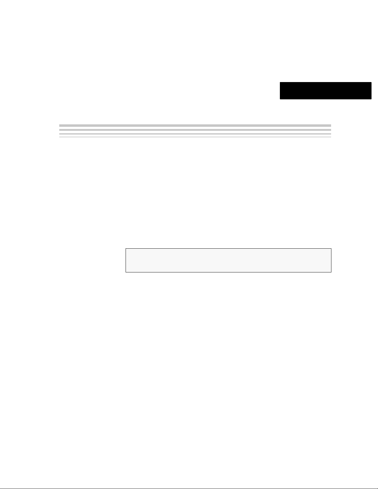
The TUSB3410 EVM is shown in Figure 1, together with typical
representations of the hardware items required for its use.
Figure 1–1.TUSB3410 Evaluation Hardware
PC
USB Cable
Serial Cable
USB EVM
1-2
Page 11
1.2 Hardware Overview
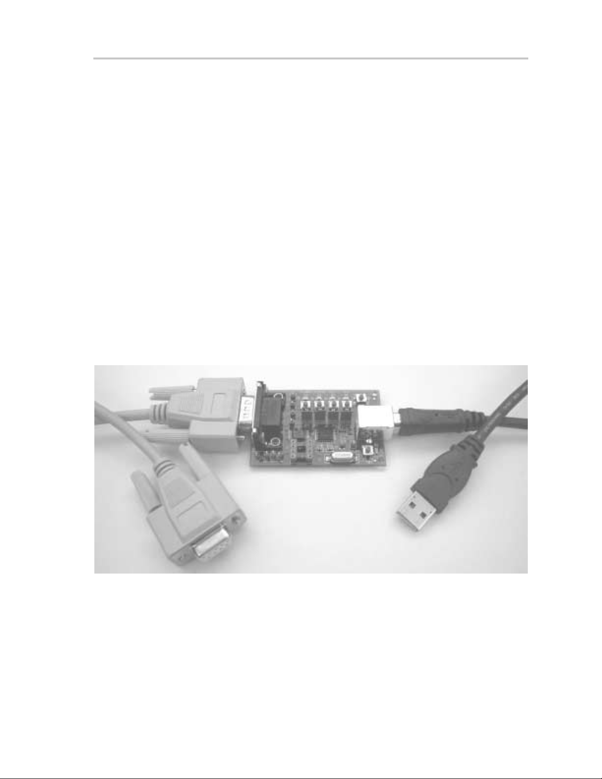
The TUSB3410 GPIO EVM hardware platform is 4,3 cm × 6,8 cm in width ×
length. Throughout this document, text inside of parentheses (ex.) is reference
designators found on the TUSB3210 EVM. See Figure 1–2 for a reference
picture of the EVM. First, all jumpers are installed with the factory settings. See
T able 2–3 for a description of jumper settings and make any required changes
before using the EVM. The TUSB3410 GPIO EVM is designed to allow great
flexibility in evaluation while being very easy and practical to use. The EVM is
designed to run using a 12-MHz crystal and an I
up for bus-powered operation using a 5-V to 3.3-V voltage regulator. The
firmware installed at the factory in the EEPROM is special USB keyboard
firmware, which makes it very easy for evaluation on any USB-enabled OS
without the need for a device driver. The firmware installed is reference
firmware and the source code is available for developers. The RS-232 port is
available for monitoring 8052 MCU activity for debugging purposes. The
RS-232 port requires a 1-to-1 cable, not a null-modem cable. Several test
points have been added to the EVM for probing. An LED (D2) displays the
suspend status of the TUSB3410 device. A USB cable should be plugged into
a USB port on a PC or USB hub and connected to the TUSB3410 EVM type-B
USB connector (U3).
Hardware Overview
2
C EEPROM. The EVM is set
Figure 1–2.TUSB3410 GPIO Evaluation Board
Required Hardware and Software
1-3
Page 12

1-4
Page 13

Chapter 2
EVM Operation
This chapter provides information required for proper operation of the
TUSB3410 GPIO EVM. This includes power and PC connection requirements, as well as descriptions of important operating features of the board,
such as switches, jumpers, and indicators.
Topic Page
2.1 TUSB3410 EVM Setup 2-2. . . . . . . . . . . . . . . . . . . . . . . . . . . . . . . . . . . . . . . . .
2.2 Interfaces and USB Ports 2-2. . . . . . . . . . . . . . . . . . . . . . . . . . . . . . . . . . . . . .
2.3 Power Supply 2-2. . . . . . . . . . . . . . . . . . . . . . . . . . . . . . . . . . . . . . . . . . . . . . . . .
2.4 Buttons 2-2. . . . . . . . . . . . . . . . . . . . . . . . . . . . . . . . . . . . . . . . . . . . . . . . . . . . . .
2.5 Light Emitting Diodes (LEDs) 2-2. . . . . . . . . . . . . . . . . . . . . . . . . . . . . . . . . .
2.6 Jumpers 2-3. . . . . . . . . . . . . . . . . . . . . . . . . . . . . . . . . . . . . . . . . . . . . . . . . . . . .
2.7 EEPROM 2-3. . . . . . . . . . . . . . . . . . . . . . . . . . . . . . . . . . . . . . . . . . . . . . . . . . . . .
EVM Operation
2-1
Page 14

TUSB3410 EVM Setup
2.1 TUSB3410 EVM Setup
The TUSB3410 general-purpose EVM is designed to support many USB
applications. The EVM comes in a default configuration that requires no
additional components on the EVM. A full description of the TUSB3410 device
is specified in the data manual. The PC must be running a USB-capable
operating system. Configure the EVM if required, based on desired settings
specified later in this section. Use a standard USB cable to connect the
TUSB3410 EVM to a downstream port of the PC or a USB hub tier.
2.2 Interfaces and USB Ports
The EVM uses a standard type-B connector for the upstream port. An I2C
serial interface is provided to access an I
embedded in the microcontroller and is connected to the RS-232 port on the
EVM. The RS-232 port connection can not be disabled by using the jumpers.
See jumper settings for more details. There are four buttons and four LEDs on
the EVM that can be used as general-purpose inputs and outputs to evaluate
how the system works.
2
C EEPROM. A UART port is
2.3 Power Supply
The TUSB3410 EVM uses USB bus power as its power supply.
2.4 Buttons
Table 2–1.Button Description
Button Button Description
SW1 System reset
SW2 Wakes up system if system is in suspend mode
SW3 General-purpose input, pulls P3.0 low if pressed
SW4 General-purpose input, pulls P3.1 low if pressed
SW5 General-purpose input, pulls P3.4 low if pressed
SW6 General-purpose input, pulls P3.3 low if pressed
2.5 Light Emitting Diodes (LEDs)
Table 2–2.LED Description
LED LED Description
D2 LED on indicates that the EVM is suspended
LED off indicates that EVM is not suspended
D3 General-purpose output, indicates status of P3.0 (RXD)
D4 General-purpose output, indicates status of P3.1 (TXD)
D5 General-purpose output, indicates status of P3.4
D6 General-purpose output, indicates status of P3.3
2-2
Page 15

2.6 Jumpers
Table 2–3 is provided to help set up and configure the EVM platform jumpers
for the desired mode of operation. The EVM can download firmware code from
the PC through a loading program (may or may not be supplied with your EVM)
2
or from an I
C EEPROM. JP2 and JP3 are used to connect P3.0 and P3.1 to
D3 and D4 respectively . JP4 is for separating the SCL pin of the I2C EEPROM
from SCL of the TUSB3410.
Table 2–3.Jumper Description
Jumper Jumper Description
JP1 Installed: connect suspend LED to SUSP pin of TUSB3410
JP2 Installed: connect LED D4 and SW4 to P3.1 (GPIO_TXD)
JP3 Installed: connect LED D3 and SW3 to P3.0 (GPIO_RXD)
JP4 Installed: connect SCL of I2C EEPROM to SCL of TUSB3410 for normal operation
Uninstalled: downloads firmware from USB instead of I
2
C EEPROM
2.7 EEPROM
The I2C EEPROM is used to provide application-specific firmware. The
TUSB3410 automatically reads the EEPROM at power up via the I
header must be added to the application firmware before loading it into the
EEPROM. See the TUSB3410 data manual for a description of the header
definition. The header can be generated automatically using the I
header-generation utility software provided with the device.
Jumpers
2
C bus. A
2
C
The EVM ships with a preprogrammed EEPROM that has keyboard controller
firmware. It enumerates properly when connected to a USB host.
EVM Operation
2-3
Page 16

2-4
Page 17

Chapter 3
Bill of Materials and EVM Layouts
This chapter describes the bill of materials and EVM layouts for the TUSB3410
EVM.
Topic Page
3.1 Bill of Materials 3-2. . . . . . . . . . . . . . . . . . . . . . . . . . . . . . . . . . . . . . . . . . . . . . .
3.2 EVM Layouts 3-3. . . . . . . . . . . . . . . . . . . . . . . . . . . . . . . . . . . . . . . . . . . . . . . . .
Bill of Materials and EVM Layouts
3-1
Page 18

Bill of Materials
3.1 Bill of Materials
Item Qty. Reference Part Part Number PCB Footprint
1 1 CN2 Connector-DB9 747250-4 DB9-HF
2 2 C21, C1 1 µF C2012X7R1C105M SMT_0805
3 1 C2 4.7 µF C3216X7R1C475M SMT_1206
4 8 C3, C6, C8, C10, C49, C50, 0.1 µF C1608X7R1H104K SMT_0603
C51, C52
5 2 C4,C5 0.01 µF C1608X7R1H103K SMT_0603
6 7 C7, C9, C53, C54, C55, C56, C57 0.001 µF C1608X7R1H102K SMT_0603
7 2 C11, C12 22 pF C1608C0G1H220J SMT_0603
8 2 C20, C19 33 pF C1608C0G1H330J SMT_0603
9 1 D1 SOT-23-diode BAS21ZXCT-ND SOT23-DIODE
10 5 D2, D3, D4, D5, D6 LED 160-1421-1-ND SMT_0805
11 1 F2 TDK MPZ2012S331A MPZ2012S331A MPZ2012
12 4 JP1, JP2, JP3, JP4 Jumper HDR1X2
13 1 R1 90.9 kΩ P100KCCT-ND SMT_0603
14 1 R2 100 kΩ P100KCCT-ND SMT_0603
15 1 R3 1.5 kΩ P1.50KCCT-ND SMT_0603
16 2 R4, R5 33 Ω P33.2CCT-ND SMT_0603
17 8 R9, R10, R14, R15, R16, R17, 1 kΩ P1.00KCCT-ND SMT_0603
R18, R19
18 1 R11 32 kΩ P32.4KCCT-ND SMT_0603
19 1 R12 10 kΩ P10.0KCCT-ND SMT_0603
20 1 R13 15 kΩ P15.0KCCT-ND SMT_0603
21 1 R20 5 kΩ P1.50KCCT-ND SMT_0603
22 1 R21 5 kΩ P10.0KCCT-ND SMT_0603
23 6 SW1, SW2, SW3, SW4, SW5, SW6 Switch 7914G-1-000E MOM-SW
24 2 TP5, TP6 T point R HDR1X1 TP52
25 2 TP7,TP8 Test point TP52
26 5 TP9, TP10, TP11, TP12, TP13 Test point, small TP52
27 1 U1 TUSB3410 TUSB3410 LQFP-32
28 1 U2 TPS76933 TPS76933DBVT SOT-5P
29 1 U3 Type B USB-shield AE1085-ND 4P-B-RECEP
30 1 U5 8-pin socket for 24LCxx A400-ND DIP8_SKT
31 1 U6 MAX3221E MAX322E T.I. MAX3221E
32 1 Y1 12-MHz crystal
HC49SMD
P-16695 CRYSTEK
3-2
Page 19
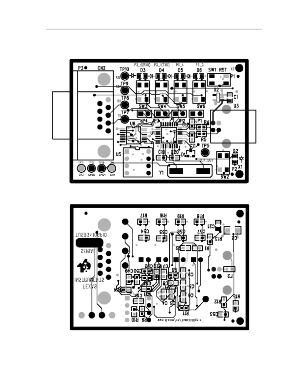
3.2 EVM Layouts
Figure 3–1.Top Layer
EVM Layouts
Figure 3–2.Bottom Layer
Bill of Materials and EVM Layouts
3-3
Page 20

3-4
Page 21

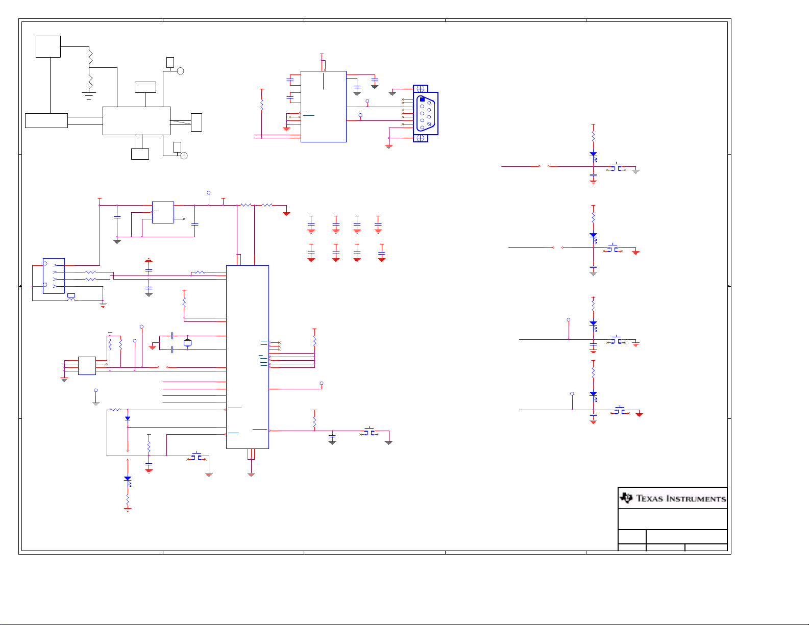
Appendix A
TUSB3410 GPIO EVM Schematic Diagram
TUSB3410 GPIO EVM Schematic Diagram
A-1
Page 22

A-2
Page 23
5
TUSB 3410 BLOCK DIAGRAM
+3V3
LDO
+1V8
D D
+5V Bus Power
USB Full
Speed
C C
Type B USB-Shield
+5V
1
6
DM
2
DP
3
GND
45
U3
F2
EARTHGND
1 2
1 2
TDK MPZ2012S331A
B B
A A
1
2
3
4
8pin Socket for 24LCxx
VDD18
33
TP6
5
+5V
8
7
6
5
1
+3V3
SUSPEND
R9
1K
R11
32K
TUSB3410
32-Pin LQFP
I2C
SDA
I2C
EPROM
C1
1uF
TP9
R10
1
1K
SCL
SDA
3
D1
1
SUSP
1 2
JP1
12
D2
R15
1K
D+
D-
R4
R5
33
U5
Vcc
A0
A1
WP
A2
SCL
SDA
Vss
CRYSTAL
12Mhz
SCL
1 5
3
2
TP10
1
+3V3
U2
IN OUT
EN
GND
TPS76933
C11
22pF
C12
22pF
JP4
SUSP
R13
15K
C21
1uF
NC/FB
LED
GPIO
LED
GPIO
GND
DP0
DM0
C2033pF
12
Push Button
Serial
Debug
Push Button
4
ESR=0.2ohm
C2
4.7uF
R3 1.5K
+3V3
R20
5K
C1933pF
Y1
12 MHz Crystal HC49SMD
GPIO1_RXD
GPIO2_TXD
GPIO3
GPIO4
ENn
RSTIn
SW1
4
+3V3
15
16
U6
2 3
C1+ V+
C51
4
0.1uF
0.1uF
C52
WAKEUP
10
12
14
11
SIN
RI
/DCD
/DSR
/CTS
CLK_OUT
C1-
5
C2+
6
C2-
1
EN
INVALID
FORCEON
GND
T1IN
9
R1OUT
MAX3221E
R21
5K
R12
10K
+3V3
+3V3
+3V3
+3V3
+3V3
R14
1K
GPIO2_TXD
GPIO1_RXD
+3V3
TP11
1
X2
X1
+3V3
U1
5
PUR
6
DP0
7
DM0
23
TEST0
24
TEST1
26
X2
27
X1/CLKI
11
SCL
10
SDA
32
P3_0
31
P3_1
30
P3_3
29
P3_4
1
VREGEN
2
SUSP
9
RESET
TUSB3410
Voltage Divider Network
R2
R1
100k
90.9k
+1V8
3
4
25
VCC
VCC
VDD1V8
DTR
RTS
SOUT/IR_SOUT
SIN/IR_SIN
RI/CP
DCD
DSR
CTS
CLKOUT
WAKEUP
GND
GND
GND
28
18
8
21
20
19
17
16
15
14
13
22
12
C3
0.1uF
C7
0.001uF
TP5
0.001uF
VCC
1
/RW
C53
FORCEOFF
T1OUT
R1IN
+3V3
+1V8 +1V8
V-
C4
0.01uF
C8
0.1uF
3
7
13
8
C49
0.1uF
C50
0.1uF
TP7
TX
1
TP8
RX
1
+3V3
+1V8
C5
0.01uF
+3V3
C9
0.001uF
SW2
/RW
CN2
GND
10
1
6
2
7
4
8
3
9
GND
5
GND
11
Connector-DB9
Receptacle
C6
0.1uF
C10
0.1uF
Serial
Debug
Port
2
Isolate TXD LED during Serial Debug
JP2
GPIO2_TXD
1 2
Isolate RXD LED during Serial Debug
GPIO4
GPIO3
JP3
1 2
GPIO1_RXD
GPIO4
TP12
1
GPIO3
TP13
0.001uF
0.001uF
0.001uF
1
0.001uF
1
+3V3
R16
1K
12
D4
P3_1
C55
D3
C54
C56
C57
SW4
+3V3
R17
1K
12
P3_0
SW3
+3V3
R19
1K
12
D5
P3_4
SW5
+3V3
R18
1K
12
D6
P3_3
SW6
TUSB 3410 GPIO
SIZE
C
4
3
2
SCALE: NONE
06/18/02
DWG NO:
Thursday, June 20, 2002
1
1 1Sheet of
 Loading...