

Page 1
NC – No internal connection
V
CC(I/O)
V
CC(5.0)
V
PU(3.3)
NC
SPEED
RCV
VP
VM
V
reg(3.3)
D+
D–
OE
NC
SOFTCON
GND
SUSPEND
1
2
3
4
14
16 1315
12
11
10
9
5
6
7
8
GND
(Exposed die pad)
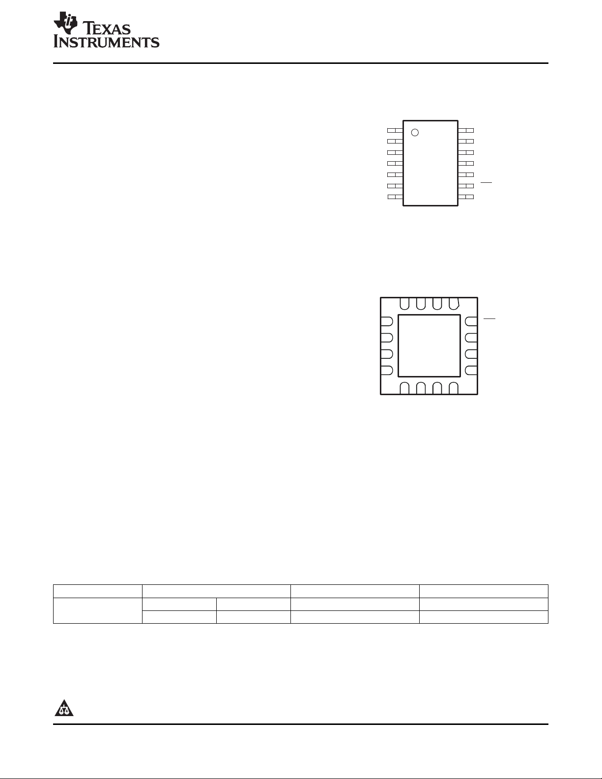
RGT PACKAGE
(BOTTOMVIEW)
PW PACKAGE
(TOP VIEW)
V
CC(I/O)
V
CC(5.0)
V
PU(3.3)
V
reg(3.3)
SPEED
RCV
VP
VM
SOFTCON
GND
D+
D–
OE
SUSPEND
1
2
3
4
5
6
14
13
12
11
10
9
7
8
www.ti.com
1
FEATURES
• Complies With Universal Serial Bus
Specification Rev. 2.0 (USB 2.0)
• Transmits and Receives Serial Data at Both
Full-Speed (12-Mbit/s) and Low-Speed
(1.5-Mbit/s) Data Rates
• Integrated Bypassable 5-V to 3.3-V Voltage
Regulator for Powering Via USB VBUS
• Low-Power Operation, Ideal for Portable
Equipment
• Meets the IEC-61000-4-2 Contact ( ± 9KV) and
Air-gap ( ± 9KV) ESD Ratings
• Separate I/O Supply With Operation Down to
1.65 V
• Very-Low Power Consumption to Meet USB
Suspend Current Requirements
• No Power-Supply Sequencing Requirements
APPLICATIONS
• Cellular Phones
• Personal Digital Assistants (PDAs)
• Handheld Computers
TUSB2551
ADVANCED UNIVERSAL SERIAL BUS TRANSCEIVER
SCES667 – FEBRUARY 2008
ORDERING INFORMATION
PACKAGE
QFN – RGT Reel of 2000 TUSB2551RGTR ZWT
TSSOP – PW Reel of 3000 TUSB2551PWR TU2551
(1) (2)
ORDERABLE PART NUMBER TOP-SIDE MARKING
. This allows the system interface to
CC(5.0)
Copyright © 2008, Texas Instruments Incorporated
DESCRIPTION/ORDERING INFORMATION
The TUSB2551 is a single-chip transceiver that complies with the physical-layer specifications of universal serial
bus (USB) 2.0. The device supports both full-speed (12-Mbit/s) and low-speed (1.5-Mbit/s) operation. The
TUSB2551 delivers superior edge rate control, producing crisper eye diagrams, which ease the task of passing
USB compliance testing.
A dual supply-voltage operation allows the TUSB2551 to reference the system interface I/O signals to a supply
voltage down to 1.6 V, while independently powered by the USB V
operate at its core voltage without the addition of buffering logic, and also reduce system operating current.
T
A
– 40 ° C to 85 ° C
(1) Package drawings, thermal data, and symbolization are available at www.ti.com/packaging .
(2) For the most current package and ordering information, see the Package Option Addendum at the end of this document, or see the TI
1
PRODUCTION DATA information is current as of publication date.
Products conform to specifications per the terms of the Texas
Instruments standard warranty. Production processing does not
necessarily include testing of all parameters.
website at www.ti.com .
Please be aware that an important notice concerning availability, standard warranty, and use in critical applications of
Texas Instruments semiconductor products and disclaimers thereto appears at the end of this data sheet.
Page 2
www.ti.com
V
CC
(5.0)
V
reg(3.3)
V
PU(3.3)
D+
D–
V
CC
(I/O)
SOFTCON
SPEED
OE
RCV
VP
VM
SUSPEND
GND
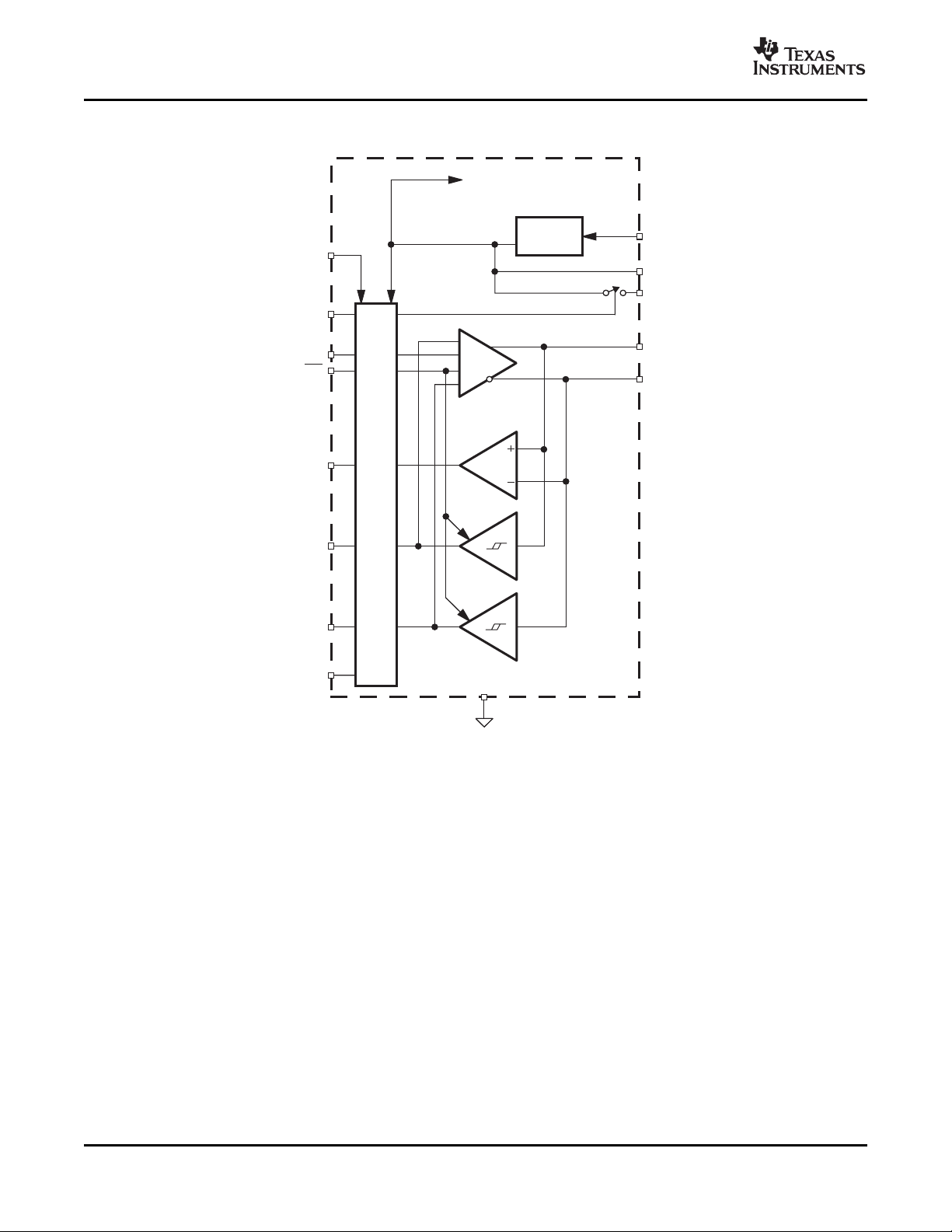
LDO
Regulator
ToInternal
Circuitry
Level
Translator
TUSB2551
ADVANCED UNIVERSAL SERIAL BUS TRANSCEIVER
SCES667 – FEBRUARY 2008
BLOCK DIAGRAM
2 Submit Documentation Feedback Copyright © 2008, Texas Instruments Incorporated
Product Folder Link(s): TUSB2551
Page 3
www.ti.com
ADVANCED UNIVERSAL SERIAL BUS TRANSCEIVER
TERMINAL FUNCTIONS
TERMINAL
NAME
V
CC(I/O)
RGT PW
NO. NO.
15 1 I
SPEED 1 2 I
RCV 2 3 O Receive data. Output for USB differential data.
VP 3 4 I/O
VM 4 5 I/O
SOFTCON 5 6 I Soft connect. Controls state of V
GND 6 7 Ground reference
SUSPEND 7 8 I Suspend. Active high. Turns off internal circuits to reduce supply current.
NC 8, 16 No internal connection
OE 9 9 I
D – , D+ 10, 11 10, 11 I/O Differential data lines conforming to the USB standard
V
reg(3.3)
V
PU(3.3)
V
CC(5.0)
12 12 O
13 13 O
14 14 I USB bus supply voltage. Used to power USB transceiver and internal circuitry.
I/O DESCRIPTION
System interface supply voltage. Used to provide reference supply voltage for system I/O
interface signaling.
Speed. Edge-rate control: A logic HIGH operates at edge rates for full-speed operation. A
logic LOW operates at edge rates for low-speed operation.
If OE = 1, VP = Receiver output (+)
If OE = 0, VP = Driver input (+)
If OE = 1, VM = Receiver output ( – )
If OE = 0, VM = Driver input ( – )
. Refer to V
PU(3.3)
PU(3.3)
Output enable. Active low. Enables the transceiver to transmit data onto the bus. When
inactive, the transceiver is in the receive mode.
3.3-V reference supply. Requires a minimum 0.1- µ F decoupling capacitor for stability. A
1- µ F capacitor is recommended.
Pullup supply voltage. Used to connect 1.5-k Ω pullup speed detect resistor. If SOFTCON =
1, V
is high impedance. If SOFTCON = 0, V
PU(3.3)
PU(3.3)
TUSB2551
SCES667 – FEBRUARY 2008
pin description for details.
= 3.3 V.
FUNCTIONAL DESCRIPTION
FUNCTION SELECTION
SUSPEND OE D+, D – RCV VP, VM FUNCTION
0 0 Driving Active Active Normal transmit mode
0 1 Receiving Active Active Normal receive mode
1 0 Hi-Z 0 Not active Low power state
1 1 Hi-Z 0 Active Receiving during suspend (low power state)
(1) During suspend, VP and VM are active in order to detect out-of-band signaling conditions.
TRUTH TABLE DURING NORMAL MODE
OE = 0
INPUT OUTPUT
VP VM D+ D – RCV
0 0 0 0 X
0 1 0 1 0 Logic 0
1 0 1 0 1 Logic 1
1 1 1 1 X
OE = 1
Input Output
D+ D – VP VM RCV
0 0 0 0 X
0 1 0 1 0 Logic 0
1 0 1 0 1 Logic 1
1 1 1 1 X
(1) X = Undefined
(1)
(1)
(1)
(1)
(1)
RESULT
SE0
Undefined
RESULT
SE0
Undefined
Copyright © 2008, Texas Instruments Incorporated Submit Documentation Feedback 3
Product Folder Link(s): TUSB2551
Page 4
www.ti.com
TUSB2551
ADVANCED UNIVERSAL SERIAL BUS TRANSCEIVER
SCES667 – FEBRUARY 2008
Power-Supply Configurations
The TUSB2551 can be used with different power-supply configurations, which can be dynamically changed. An
overview is given in Table 1 .
• Normal mode – Both V
connected to a 5-V source (4 V to 5.5 V). The internal voltage regulator then produces 3.3 V for the USB
connections. For 3.3-V operation, both V
V
is independently connected to a voltage source (1.65 V to 3.6 V), depending on the supply voltage of
CC(I/O)
the external circuit.
• Disable mode – V
CC(I/O)
internal circuits of the TUSB2551 ensure that the D+ and D – pins are in 3-state, and the power consumption
drops to the low-power (suspended) state level. Some hysteresis is built into the detection of V
• Sharing mode – V
CC(I/O)
pins are made 3-state, and the TUSB2551 allows external signals of up to 3.6 V to share the D+ and D –
lines. The internal circuits of the TUSB2551 ensure that virtually no current (maximum 10 mA) is drawn via
the D+ and D – lines. The power consumption through V
Both the VP and VM pins are driven HIGH to indicate this mode. Pin RCV is made LOW. Some hysteresis is
built into the detection of V
Configuration Mode VBUS/VTRM VIF Notes
Normal Connected Connected Normal supply configuration and operation.
Disconnect
(D+/D – sharing)
Disconnect Ground Connected
Disable Mode Connected Open Logic controlled inputs pins are Hi-Z
Prohibited Connected Ground Prohibited condition
and V
CC(I/O)
is not connected; V
is connected; V
lost.
reg(3.3)
or V
CC(5.0)
CC(5.0)
CC(5.0)
CC(5.0)
CC(5.0)
and V
and V
and V
or V
reg(3.3)
Table 1. Power-Supply Configuration Overview
Open Connected driven with
are connected. For 5-V operation, V
reg(3.3)
are connected to a 3.3-V source (3 V to 3.6 V).
reg(3.3)
and V
CC(5.0)
are connected. In this mode, the
reg(3.3)
are not connected. In this mode, the D+ and D –
drops to the low-power (suspended) state level.
CC(I/O)
VP/VM are HIGH outputs, RCV is LOW.
With OE# = 0 and SUSPEND = 1, data lines may be
external devices up to 3.6 V.
With D+, D – floating, I
VP/VM are HIGH outputs, RCV is LOW.
With D+, D – floating, I
draws less than 1 µ A.
CC(I/O)
draws less than 1 µ A.
CC(I/O)F
CC(5.0)
lost.
CC(I/O)
is
Table 2. Pin States in Disable or Sharing Mode
PINS DISABLE-MODE STATE SHARING-MODE STATE
V
/V
CC(5.0)
reg(3.3)
V
CC(I/O)
V
PU(3.3)
D+, D – High impedance High impedance
VP, VM Invalid
RCV Invalid
Inputs (SPEED, SUSPEND, OE, SOFTCON) High impedance High impedance
(1) High impedance or driven LOW
5-V input/3.3-V output, 3.3-V input/3.3-V input Not present
Not present 1.65-V to 3.6-V input
High impedance (off) High impedance (off)
(1)
(1)
H
L
4 Submit Documentation Feedback Copyright © 2008, Texas Instruments Incorporated
Product Folder Link(s): TUSB2551
Page 5
www.ti.com
TUSB2551
ADVANCED UNIVERSAL SERIAL BUS TRANSCEIVER
SCES667 – FEBRUARY 2008
Power-Supply Input Options
The TUSB2551 has two power-supply input options.
• Internal regulator – V
circuitry with 3.3 V (nominal). V
• Regulator bypass – V
and the internal circuitry is supplied directly from the V
3 V to 3.6 V to comply with the USB specification.
The supply-voltage range for each input option is specified in Table 3 .
INPUT OPTION V
Internal regualtor
Regulator bypass maximum voltage drop of 0.3 V
Electrostatic Discharge (ESD)
PIN NAME ESD TYP UNIT
D+, D – , V
All other pins Human-Body Model ± 2 kV
CC(5.0)
is connected to 4 V to 5.5 V. The internal regulator is used to supply the internal
CC(5.0)
and V
CC(5.0)
becomes a 3.3-V output reference.
reg(3.3)
reg(3.3)
are connected to the same supply. The internal regulator is bypassed,
reg(3.3)
power supply. The voltage range is
Table 3. Power-Supply Input Options
CC(5.0)
Supply input for internal regulator Voltage-reference output Supply input for digital I/O pins
(4 V to 5.5 V) (3.3 V, 300 µ A) (1.4 V to 3.6 V)
Connected to V
(2.7 V to 3.6 V)
IEC61000-4-2, Air-Gap Discharge ± 9
IEC61000-4-2, Contact Discharge ± 9 kV
Human-Body Model ± 15
with
reg(3.3)
V
reg(3.3)
Supply input Supply input for digital I/O pins
(3 V to 3.6 V) (1.4 V to 3.6 V)
V
CC(I/O)
Copyright © 2008, Texas Instruments Incorporated Submit Documentation Feedback 5
Product Folder Link(s): TUSB2551
Page 6
www.ti.com
TUSB2551
ADVANCED UNIVERSAL SERIAL BUS TRANSCEIVER
SCES667 – FEBRUARY 2008
ABSOLUTE MAXIMUM RATINGS
(1)
over operating free-air temperature range (unless otherwise noted)
MIN MAX UNIT
V
V
V
V
I
I
I
T
CC(5.0)
CC(I/O)
reg(3.3)
I
O(D+, D-)
O
I
stg
Supply voltage range – 0.5 6 V
I/O supply voltage range – 0.5 4.6 V
Regulated voltage range – 0.5 4.6 V
DC input voltage range – 0.5 V
+ 0.5 mA
CC(I/O)
Output Current (D+, D-) ± 50 mA
Output Current (all others) ± 15 mA
Input Current ± 50 mA
Storage temperature range – 65 150 ° C
(1) Stresses beyond those listed under "absolute maximum ratings" may cause permanent damage to the device. These are stress ratings
only, and functional operation of the device at these or any other conditions beyond those indicated under "recommended operating
conditions" is not implied. Exposure to absolute-maximum-rated conditions for extended periods may affect device reliability.
RECOMMENDED OPERATING CONDITIONS
PARAMETER TEST CONDITIONS MIN TYP MAX UNIT
V
CC(5.0)
V
reg(3.3)
V
CC(I/O)
V
IL
V
IH
D+, D – Input voltage on analog I/O pins 0 3.6 V
T
c
(1) Specification applies to the following pins: SUSPEND, SPEED, RCV, SOFTCON, VP, VM, OE
Supply voltage, internal regulator option 5-V operation 4 5 5.25 V
Supply voltage, regulator bypass option 3.3-V operation 3 3.3 3.6 V
I/O supply voltage 1.65 3.6 V
Low-level input voltage
High-level input voltage
(1)
(1)
V
– 0.3 0.15 V
CC(I/O)
0.85 V
CC(I/O)
CC(I/O)
V
+ 0.3 V
CC(I/O)
Junction temperature range – 40 85 ° C
V
6 Submit Documentation Feedback Copyright © 2008, Texas Instruments Incorporated
Product Folder Link(s): TUSB2551
Page 7

www.ti.com
ADVANCED UNIVERSAL SERIAL BUS TRANSCEIVER
TUSB2551
SCES667 – FEBRUARY 2008
DC ELECTRICAL CHARACTERISTICS SYSTEM AND USB INTERFACE
V
= 3.6 V, V
CC(I/O)
= 5 V (unless otherwise noted), TA= 25 C. Bold indicates specifications over temperature, – 40 ° C to
CC(5.0)
(1)
85 ° C
PARAMETER TEST CONDITIONS MIN TYP MAX UNIT
V
OH
V
OL
I
IL
I
CC(I/O)
I
CC(5.0)
I
PU(3.3)LEAK
I
CC(I/O)LEAK
V
PU(3.3)
R
SW
ESD PROTECTION
IEC-61000-4- Air-Gap Discharge 10 pulses ± 9
2
(D+, D – ,
V
CC(5.0)
(1) Specification for packaged product only
(2) Specification applies to the following pins: RCV, VP, VM, OE.
High-level output
voltage
Low-level output
voltage
Input leakage current
(2)
(2)
IOH= 20 µ A 0.9 V
IOL= 20 µ A 0.1 V
(2)
SPEED SUSPEND OE VOLTAGE LOAD
1 0 1 1 5
1 0 0 1 5
0 0 1 1 5 µ A
V
=
V
supply current
CC(I/O)
0 0 0 1 5
0 1 0 1 5
1 0 0 1 2 mA
0 0 0 260 280 µ A
CC(5.0)
5.25 V,
V
=
CC(I/O)
3.6 V
f = 6 MHz,
CL= 50 pF
f = 750 kHz,
CL= 600 pF
1 0 1 800 1100
1 0 0 3000 5000
0 0 1 230 350 µ A
V
=
V
supply current
CC(5.0)
0 1 0 130 200
1 0 0 6 10
0 0 0 4..3 5
V
0 0 0 400 700
leakage current SOFTCON = 1, V
PU(3.3)
V
leakage current V
CC(I/O)
Pullup output voltage I
V
switch
PU(3.3)
resistance
Contact Discharge 10 pulses ± 9
only)
= 3.6 V, V
CC(I/O)
= 200 µ A, V
reg(3.3)
I
= 10 mA, V
reg(3.3)
= 0 V – 5 5 µ A
PU(3.3)
= 0 V – 5 5 µ A
CC(5.0)
= 4 V to 5.25 V 3 3.3 3.6 V
CC(5.0)
= 4 V to 5.25 V 10 Ω
CC(5.0)
CC(5.0)
5.25 V,
V
=
CC(I/O)
3.6 V
f = 6 MHz,
CL= 50 pF
f = 750 kHz,
CL= 600 pF
CC(I/O)
– 5 1.5 5 µ A
V
mA
kV
Copyright © 2008, Texas Instruments Incorporated Submit Documentation Feedback 7
Product Folder Link(s): TUSB2551
Page 8
www.ti.com
TUSB2551
ADVANCED UNIVERSAL SERIAL BUS TRANSCEIVER
SCES667 – FEBRUARY 2008
DC ELECTRICAL CHARACTERISTICS TRANSCEIVER
PARAMETER TEST CONDITIONS MIN TYP MAX UNIT
LEAKAGE CURRENT
I
LO
INPUT LEVELS
V
DI
V
CM
V
SE
OUTPUT LEVELS
V
OL
V
OH
CAPACITANCE
C
IN
Z
DRV
(1) Specification for packaged product only
Hi-Z state data line leakage (suspend mode) 0 V < VIN< 3.3 V, SUSPEND = 1 – 10 10 µ A
Differential input sensitivity |(D+) – (D – )| 0.2 V
Differential common mode range Includes VDIrange 0.8 2.5 V
Single-ended receiver threshold 0.8 2 V
Receiver hysteresis 200 mV
Static output low RL= 1.5 k Ω to 3.6 V 0.3 V
Static output high RL= 15 k Ω to GND 2.8 3.6 V
Transceiver capacitance Pin to GND 10 pF
Driver output resistance Steady-state drive 1 6 11 Ω
(1)
8 Submit Documentation Feedback Copyright © 2008, Texas Instruments Incorporated
Product Folder Link(s): TUSB2551
Page 9

www.ti.com
ADVANCED UNIVERSAL SERIAL BUS TRANSCEIVER
TUSB2551
SCES667 – FEBRUARY 2008
AC ELECTRICAL CHARACTERISTICS
(1)
PARAMETER TEST CONDITIONS MIN MAX UNIT
DRIVER CHARACTERISTICS (LOW SPEED)
T
R
T
F
Transition rise time 75 300 ns
Transition fall time 75 300 ns
LRFM Rise/fall time matching TR, T
V
CRS
Output signal crossover voltage 1.3 2 V
CL= 200 pF, See Figure 2
CL= 600 pF
CL= 200 pF, See Figure 2
CL= 600 pF
F
80 125 %
DRIVER CHARACTERISTICS (FULL SPEED)
T
R
T
F
Transition rise time CL= 50 pF, See Figure 2 4 20 ns
Transition fall time CL= 50 pF, Figure 2 4 20 ns
FRFM Rise/fall time matching (TR, TF) 90 111.1 %
V
CRS
Output signal crossover voltage 1.3 2 V
TRANSCEIVER TIMING (FULL SPEED)
t
PVZ
t
PZD
t
PDZ
t
PZV
t
PLH
t
PHL
t
PLH
t
PHL
t
PLH
t
PHL
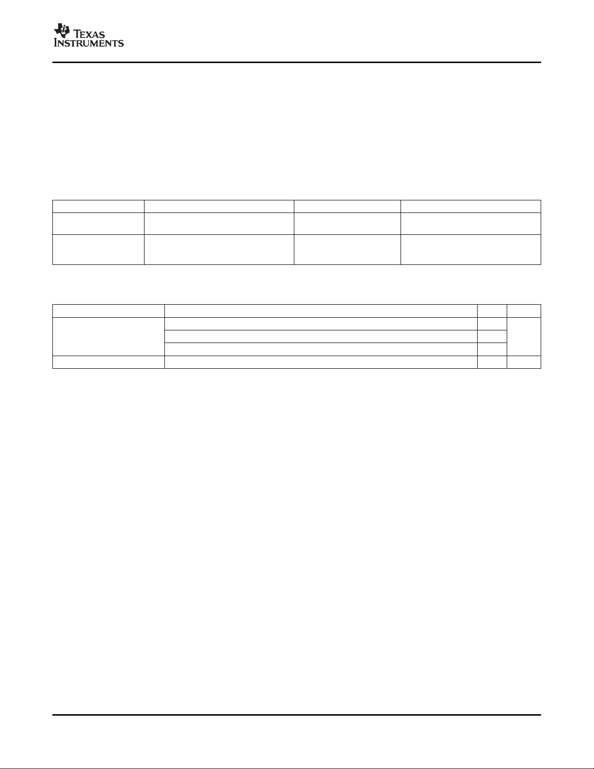
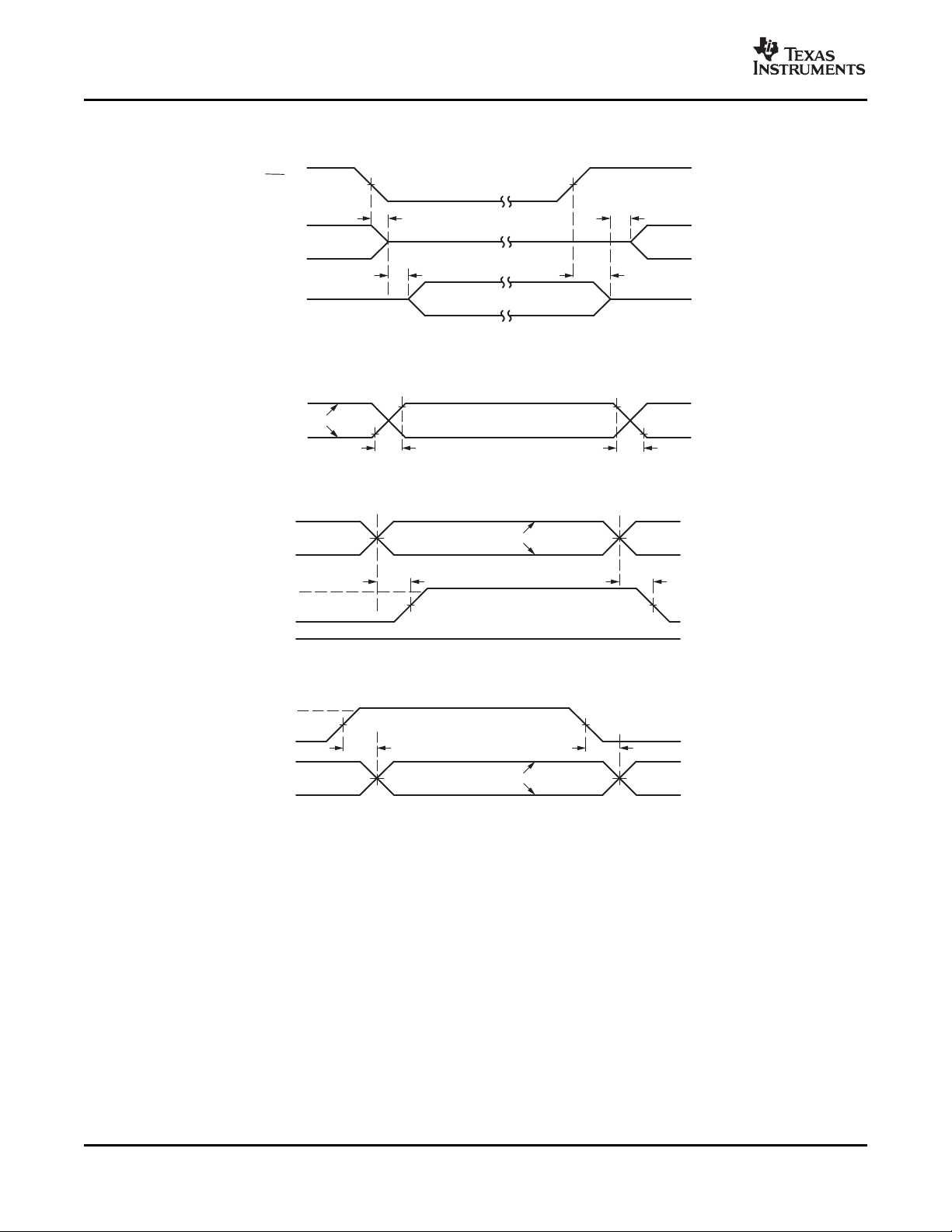
OE to receiver 3-state delay See Figure 1 15 ns
Receiver 3-state to transmit delay See Figure 1 15 ns
OE to driver 3-state delay See Figure 1 15 ns
Driver 3-state to receive delay See Figure 1 15 ns
VP, VMto D+, D – propagation delay See Figure 4 17 ns
D+, D – to RCV propagation delay See Figure 3 17 ns
D+, D – to VP, VMpropagation delay See Figure 3 10 ns
(1) Specification for packaged product only
Copyright © 2008, Texas Instruments Incorporated Submit Documentation Feedback 9
Product Folder Link(s): TUSB2551
Page 10
www.ti.com
t
PVZ
OE
VP/V
M
D+/D–
TRANSMIT
RECEIVE
t
PZD
t
PDZ
t
PZV
t
R
RISE TIME
Differential
Data Lines
10%
90%
10%
90%
t
F
FALL TIME
t
PLH
V
CRS
V
SS
V
OL
V
OH
D–
D+
V
CRS
Differential
Data Lines
t
PHL
t
PLH
V
CRS
V
OL
V
OH
D–
D+
V
CRS
Differential
Data Lines
t
PHL
TUSB2551
ADVANCED UNIVERSAL SERIAL BUS TRANSCEIVER
SCES667 – FEBRUARY 2008
TIMING DIAGRAMS
Figure 1. Enable and Disable Times
Figure 2. Rise and Fall Times
Figure 3. Receiver Propagation Delay
Figure 4. Driver Propagation Delay
10 Submit Documentation Feedback Copyright © 2008, Texas Instruments Incorporated
Product Folder Link(s): TUSB2551
Page 11
www.ti.com
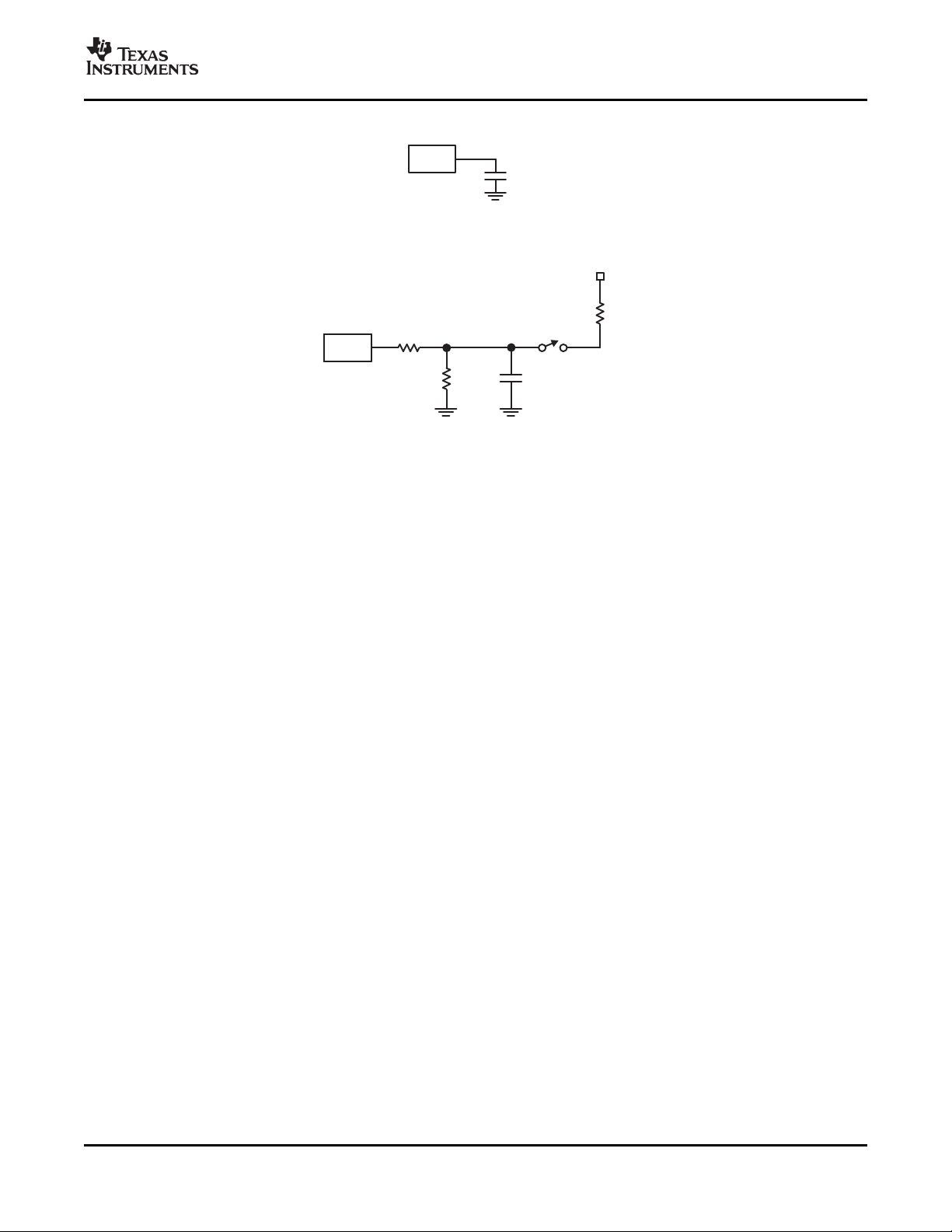
D.U.T.
25 pF
D.U.T.
C
L
15k
20
VTRM
k15
ADVANCED UNIVERSAL SERIAL BUS TRANSCEIVER
TEST CIRCUITS
Figure 5. Load for VP, VM, RCV
Figure 6. Load for D+, D –
TUSB2551
SCES667 – FEBRUARY 2008
Copyright © 2008, Texas Instruments Incorporated Submit Documentation Feedback 11
Product Folder Link(s): TUSB2551
Page 12
PACKAGE OPTION ADDENDUM
www.ti.com
17-Jul-2010
PACKAGING INFORMATION
Orderable Device
TUSB2551PW NRND TSSOP PW 14 90 Green (RoHS
TUSB2551PWG4 NRND TSSOP PW 14 90 Green (RoHS
TUSB2551PWR NRND TSSOP PW 14 2000 Green (RoHS
TUSB2551PWRG4 NRND TSSOP PW 14 2000 Green (RoHS
TUSB2551RGTR NRND QFN RGT 16 3000 TBD Call TI Call TI Samples Not Available
(1)
The marketing status values are defined as follows:
ACTIVE: Product device recommended for new designs.
LIFEBUY: TI has announced that the device will be discontinued, and a lifetime-buy period is in effect.
NRND: Not recommended for new designs. Device is in production to support existing customers, but TI does not recommend using this part in a new design.
PREVIEW: Device has been announced but is not in production. Samples may or may not be available.
OBSOLETE: TI has discontinued the production of the device.
Status
(1)
Package Type Package
Drawing
Pins Package Qty
Eco Plan
& no Sb/Br)
& no Sb/Br)
& no Sb/Br)
& no Sb/Br)
(2)
Lead/
Ball Finish
CU NIPDAU Level-1-260C-UNLIM Samples Not Available
CU NIPDAU Level-1-260C-UNLIM Samples Not Available
CU NIPDAU Level-1-260C-UNLIM Samples Not Available
CU NIPDAU Level-1-260C-UNLIM Samples Not Available
MSL Peak Temp
(3)
Samples
(Requires Login)
(2)
Eco Plan - The planned eco-friendly classification: Pb-Free (RoHS), Pb-Free (RoHS Exempt), or Green (RoHS & no Sb/Br) - please check http://www.ti.com/productcontent for the latest availability
information and additional product content details.
TBD: The Pb-Free/Green conversion plan has not been defined.
Pb-Free (RoHS): TI's terms "Lead-Free" or "Pb-Free" mean semiconductor products that are compatible with the current RoHS requirements for all 6 substances, including the requirement that
lead not exceed 0.1% by weight in homogeneous materials. Where designed to be soldered at high temperatures, TI Pb-Free products are suitable for use in specified lead-free processes.
Pb-Free (RoHS Exempt): This component has a RoHS exemption for either 1) lead-based flip-chip solder bumps used between the die and package, or 2) lead-based die adhesive used between
the die and leadframe. The component is otherwise considered Pb-Free (RoHS compatible) as defined above.
Green (RoHS & no Sb/Br): TI defines "Green" to mean Pb-Free (RoHS compatible), and free of Bromine (Br) and Antimony (Sb) based flame retardants (Br or Sb do not exceed 0.1% by weight
in homogeneous material)
(3)
MSL, Peak Temp. -- The Moisture Sensitivity Level rating according to the JEDEC industry standard classifications, and peak solder temperature.
Important Information and Disclaimer:The information provided on this page represents TI's knowledge and belief as of the date that it is provided. TI bases its knowledge and belief on information
provided by third parties, and makes no representation or warranty as to the accuracy of such information. Efforts are underway to better integrate information from third parties. TI has taken and
continues to take reasonable steps to provide representative and accurate information but may not have conducted destructive testing or chemical analysis on incoming materials and chemicals.
TI and TI suppliers consider certain information to be proprietary, and thus CAS numbers and other limited information may not be available for release.
In no event shall TI's liability arising out of such information exceed the total purchase price of the TI part(s) at issue in this document sold by TI to Customer on an annual basis.
Addendum-Page 1
Page 13
PACKAGE MATERIALS INFORMATION
www.ti.com 30-Jul-2010
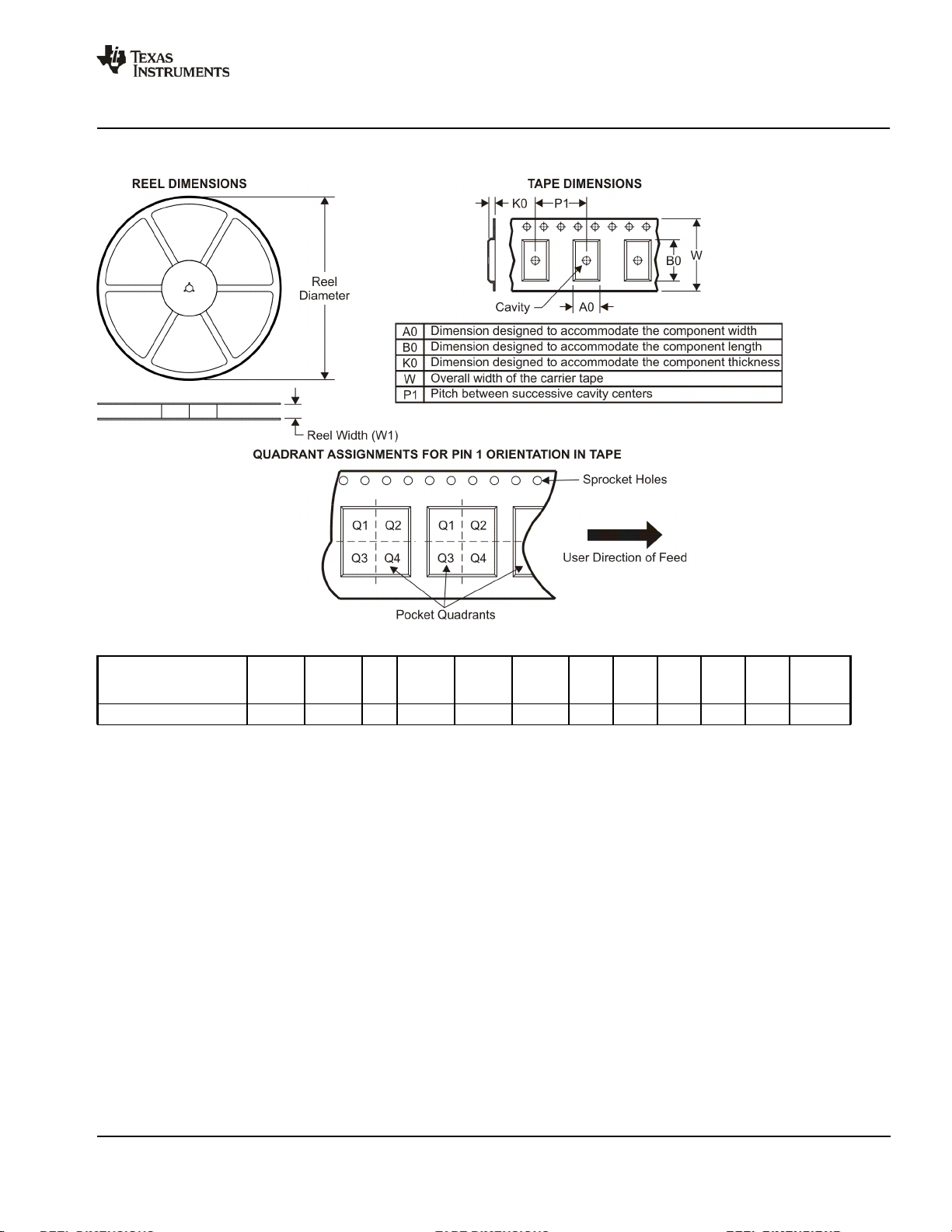
TAPE AND REEL INFORMATION
*All dimensions are nominal
Device Package
Type
TUSB2551PWR TSSOP PW 14 2000 330.0 12.4 6.9 5.6 1.6 8.0 12.0 Q1
Package
Drawing
Pins SPQ Reel
Diameter
(mm)
Reel
Width
W1 (mm)
A0
(mm)B0(mm)K0(mm)P1(mm)W(mm)
Pin1
Quadrant
Pack Materials-Page 1
Page 14

PACKAGE MATERIALS INFORMATION
www.ti.com 30-Jul-2010
*All dimensions are nominal
Device Package Type Package Drawing Pins SPQ Length (mm) Width (mm) Height (mm)
TUSB2551PWR TSSOP PW 14 2000 346.0 346.0 29.0
Pack Materials-Page 2
Page 15

Page 16

Page 17

Page 18

Page 19
Page 20

IMPORTANT NOTICE
Texas Instruments Incorporated and its subsidiaries (TI) reserve the right to make corrections, modifications, enhancements, improvements,
and other changes to its products and services at any time and to discontinue any product or service without notice. Customers should
obtain the latest relevant information before placing orders and should verify that such information is current and complete. All products are
sold subject to TI’s terms and conditions of sale supplied at the time of order acknowledgment.
TI warrants performance of its hardware products to the specifications applicable at the time of sale in accordance with TI’s standard
warranty. Testing and other quality control techniques are used to the extent TI deems necessary to support this warranty. Except where
mandated by government requirements, testing of all parameters of each product is not necessarily performed.
TI assumes no liability for applications assistance or customer product design. Customers are responsible for their products and
applications using TI components. To minimize the risks associated with customer products and applications, customers should provide
adequate design and operating safeguards.
TI does not warrant or represent that any license, either express or implied, is granted under any TI patent right, copyright, mask work right,
or other TI intellectual property right relating to any combination, machine, or process in which TI products or services are used. Information
published by TI regarding third-party products or services does not constitute a license from TI to use such products or services or a
warranty or endorsement thereof. Use of such information may require a license from a third party under the patents or other intellectual
property of the third party, or a license from TI under the patents or other intellectual property of TI.
Reproduction of TI information in TI data books or data sheets is permissible only if reproduction is without alteration and is accompanied
by all associated warranties, conditions, limitations, and notices. Reproduction of this information with alteration is an unfair and deceptive
business practice. TI is not responsible or liable for such altered documentation. Information of third parties may be subject to additional
restrictions.
Resale of TI products or services with statements different from or beyond the parameters stated by TI for that product or service voids all
express and any implied warranties for the associated TI product or service and is an unfair and deceptive business practice. TI is not
responsible or liable for any such statements.
TI products are not authorized for use in safety-critical applications (such as life support) where a failure of the TI product would reasonably
be expected to cause severe personal injury or death, unless officers of the parties have executed an agreement specifically governing
such use. Buyers represent that they have all necessary expertise in the safety and regulatory ramifications of their applications, and
acknowledge and agree that they are solely responsible for all legal, regulatory and safety-related requirements concerning their products
and any use of TI products in such safety-critical applications, notwithstanding any applications-related information or support that may be
provided by TI. Further, Buyers must fully indemnify TI and its representatives against any damages arising out of the use of TI products in
such safety-critical applications.
TI products are neither designed nor intended for use in military/aerospace applications or environments unless the TI products are
specifically designated by TI as military-grade or "enhanced plastic." Only products designated by TI as military-grade meet military
specifications. Buyers acknowledge and agree that any such use of TI products which TI has not designated as military-grade is solely at
the Buyer's risk, and that they are solely responsible for compliance with all legal and regulatory requirements in connection with such use.
TI products are neither designed nor intended for use in automotive applications or environments unless the specific TI products are
designated by TI as compliant with ISO/TS 16949 requirements. Buyers acknowledge and agree that, if they use any non-designated
products in automotive applications, TI will not be responsible for any failure to meet such requirements.
Following are URLs where you can obtain information on other Texas Instruments products and application solutions:
Products Applications
Audio www.ti.com/audio Communications and Telecom www.ti.com/communications
Amplifiers amplifier.ti.com Computers and Peripherals www.ti.com/computers
Data Converters dataconverter.ti.com Consumer Electronics www.ti.com/consumer-apps
DLP® Products www.dlp.com Energy and Lighting www.ti.com/energy
DSP dsp.ti.com Industrial www.ti.com/industrial
Clocks and Timers www.ti.com/clocks Medical www.ti.com/medical
Interface interface.ti.com Security www.ti.com/security
Logic logic.ti.com Space, Avionics and Defense www.ti.com/space-avionics-defense
Power Mgmt power.ti.com Transportation and www.ti.com/automotive
Microcontrollers microcontroller.ti.com Video and Imaging www.ti.com/video
RFID www.ti-rfid.com Wireless www.ti.com/wireless-apps
RF/IF and ZigBee® Solutions www.ti.com/lprf
TI E2E Community Home Page e2e.ti.com
Automotive
Mailing Address: Texas Instruments, Post Office Box 655303, Dallas, Texas 75265
Copyright © 2011, Texas Instruments Incorporated
 Loading...