

TUSB2040A
4-PORT HUB FOR THE UNIVERSAL SERIAL BUS
WITH OPTIONAL SERIAL EEPROM INTERFACE
SLLS288B – FEBRUARY 1998 – REVISED MARCH 1998
D
Universal Serial Bus (USB) Version 1.0
Compliant
D
Integrated USB Transceivers
D
Four Downstream Ports
D
Two Power Source Modes
– Self-Powered Mode
– Bus-Powered Mode
D
Power Switching and Overcurrent
Reporting is Provided Ganged or Per Port
D
All Downstream Ports Support Full-Speed
and Low-Speed Operations
D
Supports Suspend and Resume Operations
D
Pin-to-Pin Compatible with the TUSB2040
Device when EXTMEM Pin is Low
D
Supports Programmable Vendor ID and
Product ID With External Serial EEPROM
D
Tri-State EEPROM Interface Allows
EEPROM Sharing
D
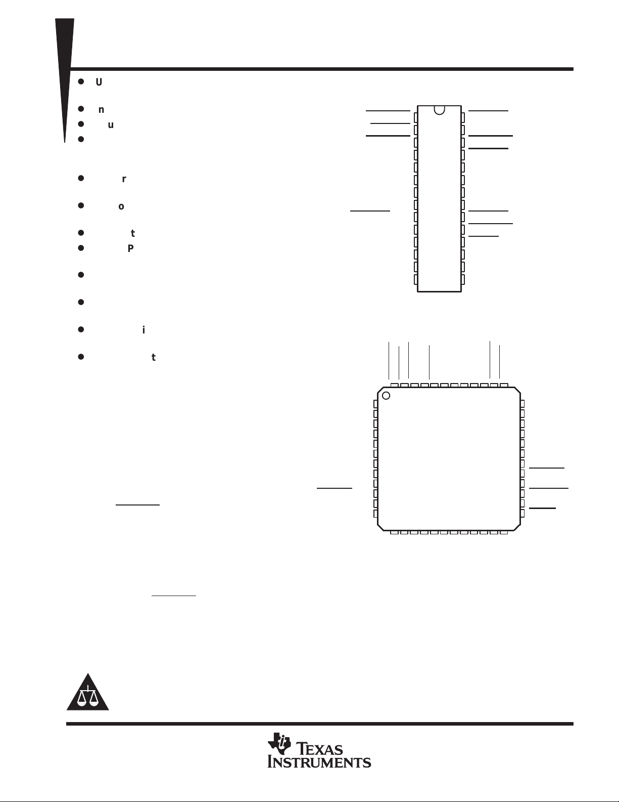
Available in 28-Pin DIP and 48-Pin TQFP
Packages
D
3.3-V Operation
description
The TUSB2040A hub is a 3.3-V CMOS device
that provides up to four downstream ports in
compliance with the USB specification 1.0
version. Pin 21 (EXTMEM) enables or disables
the EEPROM interface. When EXTMEM is low,
the TUSB2040A is functionally equivalent to the
TUSB2040 hub and the product ID (PID)
displayed during enumeration is General Purpose
USB Hub. For this configuration, pins 9 and 10 are
the BUSPWR
respectively.
If programmable vendor ID(VID) and product
ID(PID) descriptors are desired, pin 21 must be
high (EXTMEM = 1) and a SGS Thompson
M93C46 or equivalent EEPROM must be
connected to pins 9 and 10. For this configuration,
the values for BUSPWR
in the EEPROM and pins 9 and 10 become the
EEPROM interface.
and GANGED input pins,
and GANGED are stored
N PACKAGE
(TOP VIEW)
OVRCUR2
PWRON1
OVRCUR1
GND
BUSPWR
/SCL
GANGED/SDA
DP0
1
DM0
2
GND
3
NC
4
NC
5
DP1
6
DM1
7
NC
8
NC
BUSPWR
GANGED/SDA
†
JEDEC descriptor S–PQFP–G for thin quad flatpack (TQFP)
/SCL
NC
9
10
11
12
1
2
3
DP0
4
DM0
5
6
DP1
7
DM1
8
9
10
DP2
11
DM2
12
V
13
CC
14
DP3
PT PACKAGE
(TOP VIEW)
PWRON1
OVRCUR1
OVRCUR2NCPWRON2
46
474845
13141516172418
CC
DM2
NC
V
DP2
4443424140
NC
28
27
26
25
24
23
22
21
20
19
18
17
16
15
NC
DP3
NC
19
DM3
PWRON2
V
CC
OVRCUR3
PWRON3
GND
XT AL1
XT AL2
EXTMEM
PWRON4
OVRCUR4
RESET
DM4
DP4
DM3
CC
NC
OVRCUR3
NC
V
393837
202122
NC
NC
SUSPND
23
DP4
PWRON3
36
35
34
33
32
31
30
29
28
27
26
25
DM4
GND
XTAL1
XTAL2
NC
EXTMEM
NC
NC
PWRON4
NC
OVRCUR4
NC
RESET
Please be aware that an important notice concerning availability, standard warranty, and use in critical applications of
Texas Instruments semiconductor products and disclaimers thereto appears at the end of this data sheet.
PRODUCTION DATA information is current as of publication date.
Products conform to specifications per the terms of Texas Instruments
standard warranty. Production processing does not necessarily include
testing of all parameters.
POST OFFICE BOX 655303 • DALLAS, TEXAS 75265
Copyright 1998, Texas Instruments Incorporated
1

TUSB2040A
4-PORT HUB FOR THE UNIVERSAL SERIAL BUS
WITH OPTIONAL SERIAL EEPROM INTERFACE
SLLS288B – FEBRUARY 1998 – REVISED MARCH 1998
description (continued)
The TUSB2040A supports bus-power and self-power modes. The power switching to the downstream ports can
either be controlled individually or ganged using external devices to switch power and to detect overcurrent
conditions. Outputs from the external power devices provide overcurrent inputs to the TUSB2040A OVRCUR
pins and in the case of an overcurrent condition, the corresponding PWRON pins will be disabled by the
TUSB2040A. In the GANGED operation, all PWRON
can be used.
The hub requires a 48-MHz clock signal to sample data from the upstream port and generate a synchronized
12-MHz USB clock signal. The hub supports the flexibility to use any device that generates a 48-MHz clock.
Because the majority of oscillators are active devices, the low power suspend mode of the TUSB2040A will not
function because there is no way to stop the oscillator from driving the internal clock. An oscillator with a TTL
output not exceeding 3.6 V can be used by connecting its output to the XT AL1 terminal and leaving the XT AL2
terminal open. For crystal or resonator implementations, use the XTAL1 terminal as the input and the XTAL2
terminal as the feedback path. Because the crystal is required to resonate at 48 MHz, a tuning circuit as shown
in Figure 8 may be required.
The upstream port and all downstream ports are USB-compliant transceivers. Every downstream port supports
both full-speed and low-speed connections by automatically setting the slew rate according to the speed of the
device attached to the port.
signals transition simultaneously , and any OVRCUR input
2
POST OFFICE BOX 655303 • DALLAS, TEXAS 75265
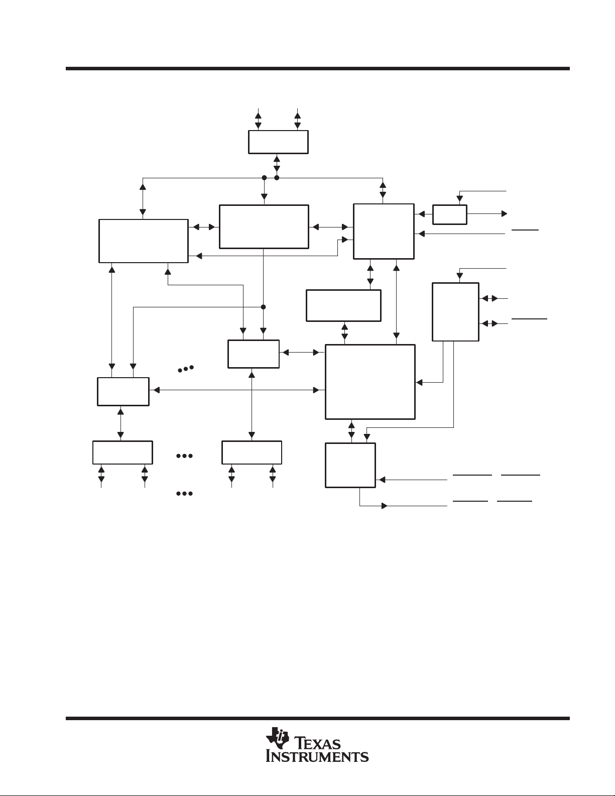
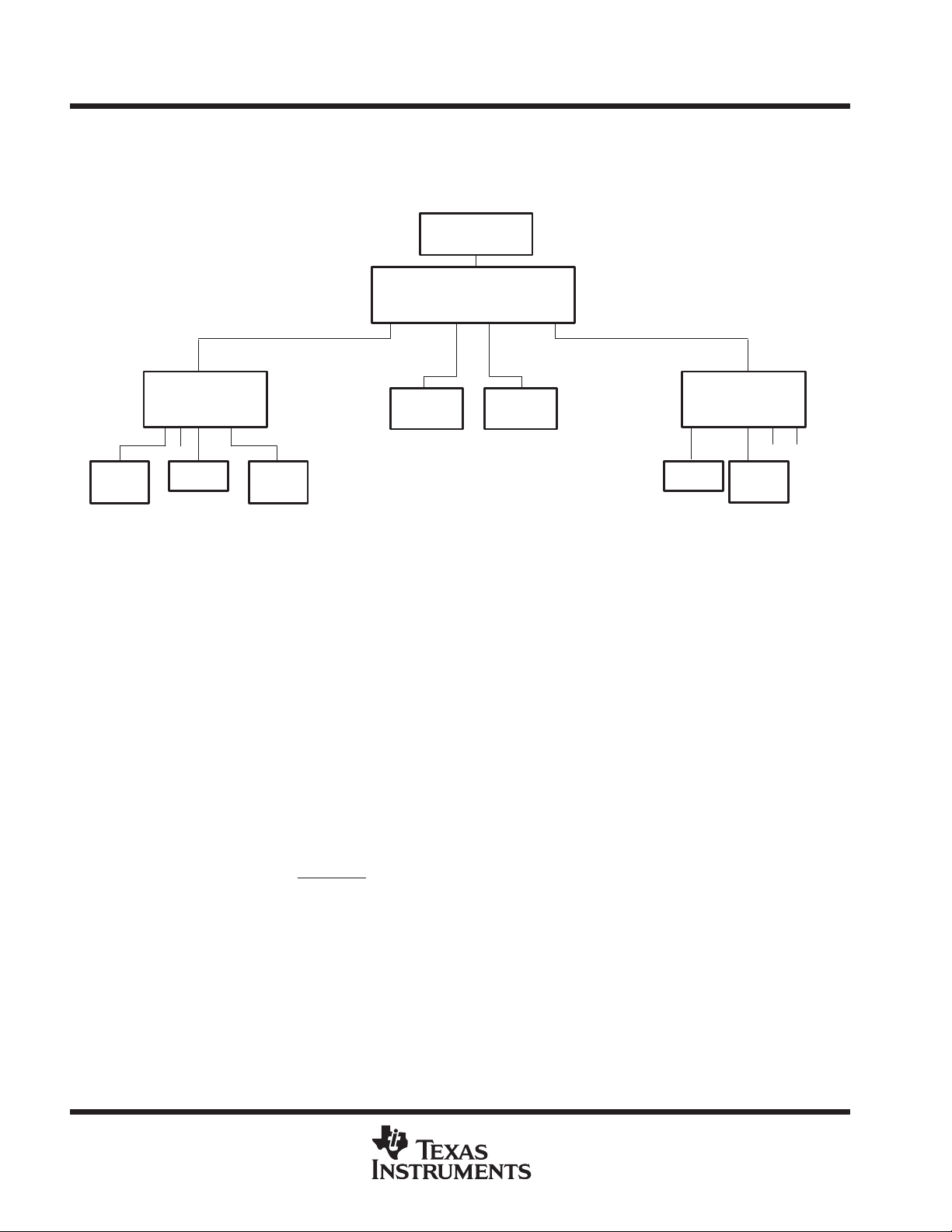
functional block diagram
Hub Repeater
DP0 DM0
45
USB
Transceiver
Suspend/Resume
Logic and
Frame Timer
TUSB2040A
4-PORT HUB FOR THE UNIVERSAL SERIAL BUS
WITH OPTIONAL SERIAL EEPROM INTERFACE
SLLS288B – FEBRUARY 1998 – REVISED MARCH 1998
23
XTAL1
OSC
SIE
22
18
21
XTAL2
RESET
EXTMEM
Port 1
Logic
Port 4
Logic
USB
Transceiver
16 17 7 8
DP4 DM4 DP1 DM1
NOTE: Terminal numbers shown are for the N package.
USB
Transceiver
SIE Interface
Logic
Hub/Device
Command
Decoder
Hub
Power
Logic
3, 1, 26, 19
2, 28, 25, 20
Serial
10
EEPROM
Interface
OVRCUR1 – OVRCUR4
PWRON1 – PWRON4
GANGED/SDA
9
BUSPWR
/SCL
POST OFFICE BOX 655303 • DALLAS, TEXAS 75265
3
TUSB2040A
I/O
DESCRIPTION
4-PORT HUB FOR THE UNIVERSAL SERIAL BUS
WITH OPTIONAL SERIAL EEPROM INTERFACE
SLLS288B – FEBRUARY 1998 – REVISED MARCH 1998
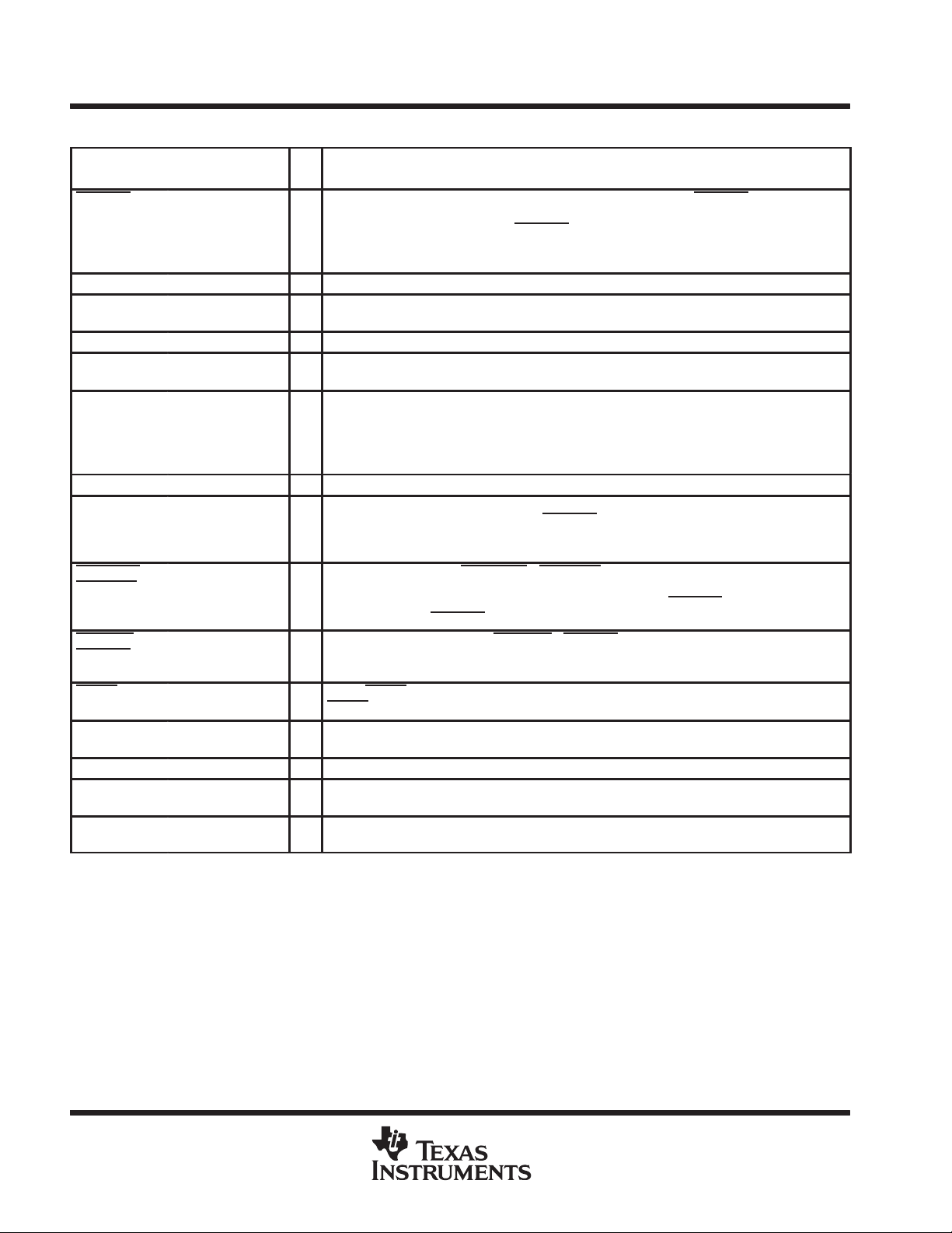
Terminal Functions
TERMINAL
NAME NPT
BUSPWR/SCL 9 10 I/O Power source input/EEPROM serial clock. When EXTMEM is low, BUSPWR/SCL is an active
DM0 5 2 I/O Root port USB differential data minus. DM0 paired with DP0 constitutes the upstream USB port.
DM1 – DM4 8, 12,
DP0 4 1 I/O Root port USB differential data plus. DP0 paired with DM0 constitutes the upstream USB port.
DP1 – DP4 7, 11,
GANGED/SDA 10 11 I/O Power switching and overcurrent detection mode/EEPROM serial data I/O. When EXTMEM is
GND 6, 24 3, 36 Ground. GND terminals must be tied to ground for proper operation.
EXTMEM 21 32 I EEPROM read enable. When EXTMEM is low, it disables the serial EEPROM interface of the
OVRCUR1 –
OVRCUR4
PWRON1 –
PWRON4
RESET 18 25 I Reset. RESET is an active low TTL input with hysteresis and must be asserted at power up. When
SUSPND 20 O Suspend status. SUSPND is an active high output that is available for external logic power down
V
CC
XTAL1 23 35 I Crystal 1. XTAL1 is a 48-MHz crystal input with 50% duty cycle. Operation at 48-MHz is four times
XTAL2 22 34 O Crystal 2. XTAL2 is a 48-MHz crystal output. Operation at 48-MHz is four times the USB full-speed
15, 17
14, 16
3, 1,
26, 19
2, 28,
25, 20
13, 27 15, 41 3.3-V supply voltage
7, 14,
19, 24
6, 13,
18, 23
48, 46,
38, 27
47, 44,
37, 29
low input that indicates whether the ports and the hub derive power from the bus or the local
supply. When EXTMEM is high, BUSPWR
EEPROM with a 100 µA internal pulldown. This standard TTL input must not change dynamically
during operation.
I/O USB differential data minus. DM1 – DM4 paired with DP1 – DP4 support up to four downstream
USB ports.
I/O USB differential data plus. DP1 – DP4 paired with DM1 – DM4 support up to four downstream
USB ports.
low, GANGED/SDA selects between gang or per port switching for the overcurrent detection of
the downstream ports. When EXTMEM is high, GANGED/SDA acts as a tri-state serial data I/O
to and from the EEPROM with a 100 µA internal pull-down. This standard TTL input must not
change dynamically during operation.
device. Pins 9 and 10 are configured as BUSPWR
is high, it enables the serial EEPROM interface and pins 9 and 10 are configured as SCL and
SDA, respectively.
I Overcurrent indicators. OVRCUR1 – OVRCUR4 are active low, standard TTL inputs. One
overcurrent indicator is available for each of the four downstream ports. In GANGED mode, one
implementation is to tie these inputs together . Alternatively , one OVRCUR
with the remaining OVRCUR
O Power-on/-off control signals. PWRON1 – PWRON4 are active low, open-drain outputs. One
power-on/-off control switch is used for each of the four downstream ports. In GANGED mode,
all outputs are switched together.
RESET
is asserted, it initializes all logic.
operations. During the SUSPEND mode, SUSPND is high. SUSPND is low for normal operation.
the USB full-speed bit rate of 12 Mbps.
bit rate of 12 Mbps. This terminal is left open when using an oscillator.
pins tied to VCC.
/SCL acts as a tri-state serial clock output to the
and GANGED, respectively. When EXTMEM
input pin may be used
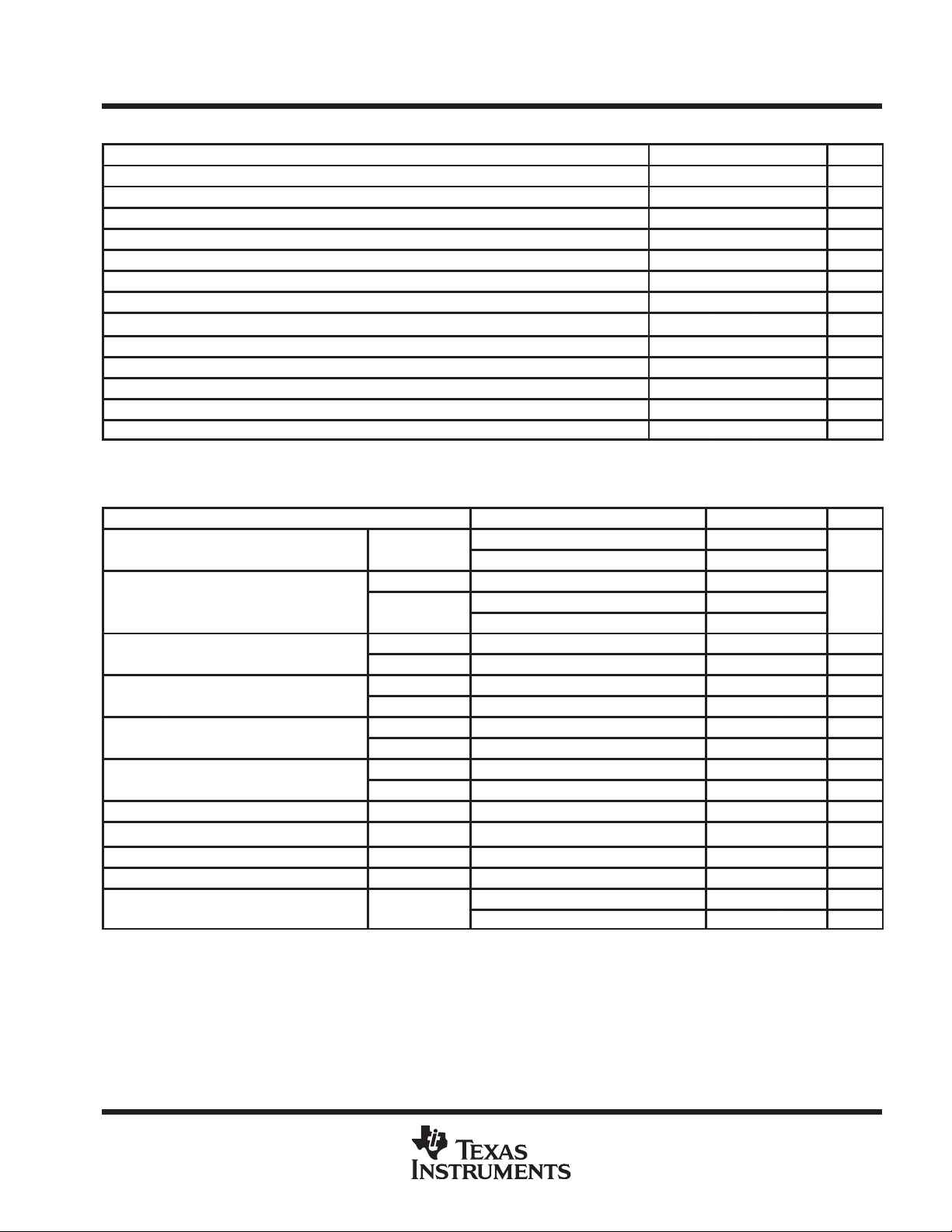
absolute maximum ratings over operating free-air temperature range (unless otherwise noted)
Supply voltage range, V
Input voltage range, V
Output voltage range, V
Input clamp current, I
Output clamp current, I
Storage temperature range, T
†
Stresses beyond those listed under “absolute maximum ratings” may cause permanent damage to the device. These are stress ratings only, and
functional operation of the device at these or any other conditions beyond those indicated under “recommended operating conditions” is not
implied. Exposure to absolute-maximum-rated conditions for extended periods may affect device reliability.
NOTE 1: All voltage levels are with respect to GND.
4
(see Note 1) –0.5 V to 3.8 V. . . . . . . . . . . . . . . . . . . . . . . . . . . . . . . . . . . . . . . . . . . . .
CC
–0.5 V to VCC + 0.5 V. . . . . . . . . . . . . . . . . . . . . . . . . . . . . . . . . . . . . . . . . . . . . . . . . . . . . .
I
–0.5 V to VCC + 0.5 V. . . . . . . . . . . . . . . . . . . . . . . . . . . . . . . . . . . . . . . . . . . . . . . . . . . .
O
, (VI < 0 V or VI > VCC) ±20 mA. . . . . . . . . . . . . . . . . . . . . . . . . . . . . . . . . . . . . . . . . . . . .
IK
, (VO < 0 V or V
OK
–65°C to 150°C. . . . . . . . . . . . . . . . . . . . . . . . . . . . . . . . . . . . . . . . . . . . . . . . . . .
stg
POST OFFICE BOX 655303 • DALLAS, TEXAS 75265
> VCC) ±20 mA. . . . . . . . . . . . . . . . . . . . . . . . . . . . . . . . . . . . . . . . .
O
†
VOHHigh-level output voltage
USB data lines
V
USB data lines
V
Positi
V
N
V
I
(V
VT–)
IOZHigh-impedance output current
ICCInput supply current
TUSB2040A
4-PORT HUB FOR THE UNIVERSAL SERIAL BUS
WITH OPTIONAL SERIAL EEPROM INTERFACE
SLLS288B – FEBRUARY 1998 – REVISED MARCH 1998
recommended operating conditions
MIN NOM MAX UNIT
Supply voltage, V
Input voltage, TTL/LVCMOS, V
Output voltage, TTL/LVCMOS, V
High-level input voltage, signal-ended receiver, V
Low-level input voltage, signal-ended receiver, V
High-level input voltage, TTL/LVCMOS, V
Low-level input voltage, TTL/LVCMOS, V
Operating free-air temperature, T
External series, differential driver resistor, R
Operating (dc differential driver) high speed mode, f
Operating (dc differential driver) low speed mode, f
Common mode, input range, differential receiver , V
Input transition times, tt, TTL/LVCMOS 0 6 ns
CC
I
O
IH(REC)
IL(REC)
IH(TTL)
IL(TTL)
A
(DRV)
(OPRH)
(OPRL)
(ICR)
electrical characteristics over recommended ranges of operating free-air temperature and supply
voltage (unless otherwise noted)
3 3.3 3.6 V
0 V
0 V
2 V
2 V
0 70 °C
22 (–5%) 22 (+5%) Ω
0.8 2.5 V
CC
CC
CC
0.8 V
CC
0.8 V
12 Mb/s
1.5 Mb/s
V
V
V
V
PARAMETER TEST CONDITIONS MIN MAX UNIT
p
V
OL
IT+
IT–
hys
I
IL
I
IH
z
o(DRV)
V
ID
†
Applies for input buffers with hysteresis
‡
Applies for open drain buffers
Low-level output voltage
ve input threshold voltage
egative-input threshold voltage
nput hysteresis†
p
Low-level input current TTL/L VCMOS VI = GND –1 µA
High-level input current TTL/LVCMOS VI = V
Driver output impedance USB data lines Static VOH or V
Differential input voltage USB data lines 0.8 V ≤ V
p
pp
T+
p
–
R
= 15 kΩ, to GND 2.8 3.6
(DRV)
IOH = –12 mA (without R
TTL/LVCMOS IOL = 4 mA 0.5
R
= 1.5 k Ω to 3.6 V 0.3
(DRV)
IOL = 12 mA (without R
TTL/LVCMOS 2 V
Single-ended
TTL/LVCMOS 0.8 V
Single-ended
TTL/LVCMOS 0.25 0.7 V
Single-ended 0.8 V ≤ V
TTL/LVCMOS V = VCC or GND‡ ±10 µA
USB data lines 0 V ≤ VO ≤ V
0.8 V ≤ V
0.8 V ≤ V
Normal operation 100 mA
Suspend mode 1 µA
≤ 2.5 V 1.8 V
ICR
≤ 2.5 V 1 V
ICR
≤ 2.5 V 300 500 mV
ICR
CC
CC
OL
≤ 2.5 V 0.2 V
ICR
) VCC –
(DRV)
) 0.5
(DRV)
7.1 19.9 Ω
0.5
±10 µA
1 µA
V
POST OFFICE BOX 655303 • DALLAS, TEXAS 75265
5
TUSB2040A
4-PORT HUB FOR THE UNIVERSAL SERIAL BUS
WITH OPTIONAL SERIAL EEPROM INTERFACE
SLLS288B – FEBRUARY 1998 – REVISED MARCH 1998
differential driver switching characteristics over recommended ranges of operating free-air
temperature and supply voltage, C
full speed mode
PARAMETER TEST CONDITIONS MIN MAX UNIT
t
r
t
f
t
(RFM)
V
O(CRS)
low speed mode
t
r
t
f
t
(RFM)
V
O(CRS)
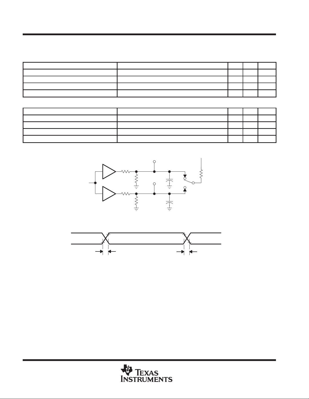
Transition rise time for DPor DM See Figure 1 and Figure 2 4 20 ns
Transition fall time for DPor DM See Figure 1 and Figure 2 4 20 ns
Rise/fall time matching (tr/tf) x 100 90 110 %
Signal crossover output voltage 1.3 2.0 V
PARAMETER TEST CONDITIONS MIN MAX UNIT
Transition rise time for DPto DM CL = 50 pF to 350 pF, See Figure 1 and Figure 2 75 300 ns
Transition fall time for DPto DM CL = 50 pF to 350 pF, See Figure 1 and Figure 2 75 300 ns
Rise/fall time matching (tr/tf) x 100 80 120 %
Signal crossover output voltage CL = 50 pF to 350 pF 1.3 2.0 V
= 50 pF unless otherwise noted (see Figures 1 and 2)
L
DM
DP
DP
DM
Characterization
measurement point
22 Ω
15 kΩ
22 Ω
15 kΩ
V(
TERM)
Full
C
L
Low
C
L
Figure 1. Differential Driver Switching Load
10%
90%
t
r
90%
10%
Figure 2. Differential Driver Timing Waveforms
= 2.8 V
1.5 kΩ
t
f
V
OH
V
OL
6
POST OFFICE BOX 655303 • DALLAS, TEXAS 75265

TUSB2040A
4-PORT HUB FOR THE UNIVERSAL SERIAL BUS
WITH OPTIONAL SERIAL EEPROM INTERFACE
SLLS288B – FEBRUARY 1998 – REVISED MARCH 1998
1.5
1.3
1
0.5
0.2
– Differential Receiver Input Sensitivity – V
ID
V
0
012
0.8
V
– Common Mode Input Range – V
ICR
34
2.5
3.6
Figure 3. Differential Receiver Input Sensitivity vs. Common Mode Input Range
V
V
V
0 V
CC
IH
IL
IT–
V
hys
Logic high
V
IT+
V
Logic low
Figure 4. Single-Ended Receiver Input Signal Parameter Definitions
POST OFFICE BOX 655303 • DALLAS, TEXAS 75265
7
TUSB2040A
4-PORT HUB FOR THE UNIVERSAL SERIAL BUS
WITH OPTIONAL SERIAL EEPROM INTERFACE
SLLS288B – FEBRUARY 1998 – REVISED MARCH 1998
APPLICATION INFORMATION
A major advantage of USB is the ability to connect 127 functions configured in up to six logical layers (tiers) to
a single personal computer (see Figure 5).
PC
With Root Hub
Monitor
Modem T elephone
With 4-Port Hub
(Self-Powered)
Scanner
Printer
Digital
Scanner
Left
Speaker
Keyboard
With 4-Port Hub
(Bus-Powered)
Mouse
With 4-Port Hub (Self-Powered)
Right
Speaker
Figure 5. USB Tiered Configuration Example
Another advantage of USB is that all peripherals are connected using a standardized four wire cable that
provides both communication and power distribution. The three power configurations are bus-powered,
self-powered and high-powered modes. For all three configurations, 100 mA is the maximum current that may
be drawn from the USB 5-V line during power up. For the bus-powered mode, a hub can draw a maximum of
500 mA from the 5-V line of the USB cable. A bus-powered hub must always be connected downstream to a
self-powered hub unless it is the only hub connected to the PC and there are no high-powered functions
connected downstream. In the self-powered mode, the hub is connected to its own power supply and can supply
up to 500 mA to each downstream port. High-powered functions may draw a maximum of 500 mA and may only
be connected downstream to self-powered hubs.
Both bus-powered and self-powered hubs require overcurrent protection for all downstream ports. The two
types of protection are individual port management (individual port basis) or ganged port management (multiple
port basis). Individual port management requires power management devices for each individual downstream
port, but adds robustness to the USB system because, in the event of an overcurrent condition, the USB host
powers down the port that has the condition. The ganged configuration uses fewer power management devices
and thus has lower system costs, but in the event of an overcurrent condition on any of the downstream ports,
all the ganged ports are disabled by the USB host.
Using a combination of the BUSPWR
and GANGED inputs, the TUSB2040A supports four modes of power
management: bus-powered hub with either individual port power management, or ganged port power
management and the self-powered hub with either individual port power management, or ganged port power
management. Texas Instruments supplies the complete hub solution because we offer this TUSB2040A, the
TUSB2070 (7–port) and the TUSB2140A (4-port with I
2
C) hubs along with the power management chips
needed to implement a fully USB Specification 1.0 compliant system.
8
POST OFFICE BOX 655303 • DALLAS, TEXAS 75265

TUSB2040A
4-PORT HUB FOR THE UNIVERSAL SERIAL BUS
WITH OPTIONAL SERIAL EEPROM INTERFACE
SLLS288B – FEBRUARY 1998 – REVISED MARCH 1998
APPLICATION INFORMATION
USB design notes
The following sections provide block diagram examples of how to implement the TUSB2040A device. Please
note, even though no resistors are shown, pull-up, pull-down and series resistors must still be used to properly
implement this device. Figure 1 shows a few resistors that must be used for the USB lines, and for a general
reference design, one is available on the TI USB web site.
Figure 6 is a block diagram example of how to connect the external EEPROM if configurable Product ID and
Vendor ID are desired. Please note that the pin numbers in Figure 6 are for the DIP package.
Figure 7 and 8 are examples of how to generate the 48-MHz clock signal. Figure 9 shows the EEPROM Read
Operation Timing Diagram. Figures 10, 1 1 and 12 illustrate how to connect the TUSB2040A device for different
power source and port power management combinations.
TUSB2040A USB Hub
48-MHz Clock
3.3 V
System
Power-On Reset
EEPROM
6
ORG
8
V
CC
5
V
SS
†
Figures 7 and 8 are two examples of how to generate the 48-MHz clock signal.
‡
Pin numbers shown are for the N package.
3
D
4
Q
2
C
S
1
Signal
1 kΩ
†
23
22
18
21
4
5
10
9
XTAL1
XTAL2
RESET
EXTMEM
DP0
DM0
SDA
SCL
V
GND
DP1 – DP4
DM1 – DM4
OVRCUR1
OVRCUR4
PWRON1 –
PWRON4
CC
–
Figure 6. Typical Application of the TUSB2040 USB Hub
13, 27
6, 24
7, 11, 14, 16
8, 12, 15, 17
3, 1, 26, 19
2, 28, 25, 20
Regulator
5 V GND
Power
Switching
Bus or Local Power
4
4
4
GND
4
V
bus
USB Data lines
and Power to
Downstream
Ports
XTAL1
Ceralock
Resonator
220 Ω
XTAL2
NOTE A: A simple way to achieve the required 48-MHz clock signal is to use a resonator such as the Ceralock resonator in Figure 7.
MuRata Electronics, Inc. manufactures a surface mount version, P/N CSACV48.00MXJ040, and a dip version, P/N
CSA48.00MXZ040. The 220 Ω resistor is used to tune the 48-MHz signal. The circuit functions properly without the capacitors,
but in order to decrease EMI emissions, the capacitors are used to decrease the amplitude of the signal. The exact values of the
capacitors are dependent on the capacitance of the board layout. Increasing the capacitance decreases the amplitude of the clock
signal. For the 4-layer PCB tested, 22 pF capacitors were used. If the capacitors are too large, the amplitude of the clock signal
will not be large enough for the successful numeration of the TUSB2040A by the USB host.
Figure 7. Resonator Clock Circuit
Ceralock is a trademark of MuRata Electronics Incorporated
POST OFFICE BOX 655303 • DALLAS, TEXAS 75265
9

TUSB2040A
4-PORT HUB FOR THE UNIVERSAL SERIAL BUS
WITH OPTIONAL SERIAL EEPROM INTERFACE
SLLS288B – FEBRUARY 1998 – REVISED MARCH 1998
APPLICATION INFORMATION
R70
2.2 kΩ
XTAL1
C66
Y1
47 pF
XTAL2
C68
1000 pF
L1 5.6 µH
NOTE B: This application shows a third harmonic 48-Mhz crystal, P/N HC-18/U 48-MHz, manufactured by US Crystal, Inc. Since the first
harmonic of most crystals is not 48-MHz, a tuning circuit such as this must be used to tune the crystal to the required 48-MHz clock
signal. When tuning the crystal (Y1) for different board implementations, the capacitor (C67) and the resistor (R70) are subject to
change and the other components should remain the same.
C67
12 pF
Figure 8. Crystal Tuning Circuit
programming the EEPROM
An SGS Thompson M93C46 EEPROM or equivalent is used for storing the programmable VID and PID. When
the EEPROM interface is enabled (EXTMEM = 1), the SCL and SDA are internally pulled down (100 µA) inside
the TUSB2040A. However , in low-power suspend mode, the BUSPWR
/SCL pin must be externally pulled down
because the internal pulldowns are disabled. The internal pulldowns are also disabled when the EEPROM
interface is disabled (EXTMEM = 0).
The EEPROM is programmed with the three 16-bit locations as shown in Table 1. Connecting pin 6 of the
EEPROM high (ORG = 1) organizes the EEPROM memory into 64×16 bit words.
Table 1. EEPROM Memory Map
ADDRESS D15 D14 D13 D12–D8 D7–D0
00000 0
00001 VID High-byte VID Low-byte
00010 PID High-byte PID Low-byte
GANGED BUSPWR 00000 00000000
XXXXXXXX
The D and Q signals of the EEPROM must be tied together using a 1 kΩ resistor with the common I/O operations
forming a single-wire bus. After system power-on reset, the TUSB2040A performs a one-time access read
operation from the EEPROM if the EXTMEM pin is pulled high and the chip select of the EEPROM is connected
to the system power-on reset. Initially , the SDA pin will be driven by the TUSB2040A to send a start bit (1) which
is followed by the read instruction (10) and the starting-word address (00000). Once the read instruction is
received, the instruction and address are decoded by the EEPROM, which then sends the data to the output
shift register. At this point, the hub stops driving the SDA pin and the EEPROM starts driving. A dummy (0) bit
is then output and the first three 16-bit words in the EEPROM are output with the most significant bit (MSB) first.
The output data changes are triggered by the rising edge of the clock provided by the TUSB2040A on the SCL
pin. The
SGS-Thompson M936C46
EEPROM is recommended because it advances to the next memory
location by automatically incrementing the address internally. Any EEPROM used must have the automatic
internal address advance function. After reading the three words of data from the EEPROM, the TUSB2040A
puts the EEPROM interface into a high-impedance condition (pulled down internally) to allow other logic to share
the EEPROM. The EEPROM read operation is summarized in Figure 9. For more details on EEPROM
operation, refer to
10
SGS-Thompson Microelectronics M93C46 Serial Microwire Bus EEPROM
POST OFFICE BOX 655303 • DALLAS, TEXAS 75265
data sheet.

Pull Down
TRI-STATED
With Internal
TUSB2040A
4-PORT HUB FOR THE UNIVERSAL SERIAL BUS
WITH EEPROM INTERFACE
SLLS288B – FEBRUARY 1998 – REVISED MARCH 1998
MSB of
Fourth Word
LSB of
Third Word
Other
Data Bits
EEPROM Driving Data LineHub Driving Data Line
D15 D14 D0 XX
6 Bit Address (000000)Start Read OP Code(10) 48 Data Bits Don’t Care
First Word
MSB of The
Bit
A0 Dummy
Bits
Other
Address
A5 A1
Figure 9. EEPROM Read Operation Timing Diagram
S
POST OFFICE BOX 655303 DALLAS, TEXAS 75265
C
D
• 11

TUSB2040A
4-PORT HUB FOR THE UNIVERSAL SERIAL BUS
WITH OPTIONAL SERIAL EEPROM INTERFACE
SLLS288B – JANUARY 1998 – REVISED MARCH 1998
APPLICATION INFORMATION
bus-powered hub, ganged port power management
A bus-powered TUSB2040A supports up to four downstream ports and is capable of supplying 100 mA of
current for low-power device class functions to each downstream port. Bus-powered hubs must implement
power switching. Ganged power management (see Figure 10) utilizes the TPS2014 power switch device and
provides overcurrent protection for downstream ports. Individual SN75240 transient suppressors reduce
in-rush current and voltage spikes. The TPS7133 low-dropout voltage regulator provides a power good (PG)
signal for reset at power up. OVRCUR1
– OVRCUR4 inputs can be tied together for ganged mode operation.
TUSB2040A
Upstream
Port
D +
D –
5 V
GND
SN75240
A
B
4.7 µF
0.1 µF
48-MHz Clock
Signal
‡
†
C
D
TPS7133
5 V
3.3 V
GND
PG
†
4.7 µF
DP0
DM0
V
CC
XTAL1
XTAL2
EXTMEM
RESET
GND
BUSPWR/SCL
GANGED/SDA
DP1
DM1
DP2
DM2
DP3
DM3
DP4
DM4
PWRON1
PWRON2
PWRON3
PWRON4
OVRCUR1
OVRCUR2
OVRCUR3
OVRCUR4
3.3 V
TPS2014
EN IN
OC
OUT
ABC
SN75240
ABC
SN75240
†
D
D
1 µF
Downstream
Ports
D +
Ferrite Beads
†
120 µF
†
Ferrite Beads
120 µF
Ferrite Beads
120 µF
Ferrite Beads
D –
GND
5 V
§
D +
D –
GND
5 V
§
D +
D –
GND
5 V
§
D +
D –
GND
†
TPS2014, TPS7133, and SN75240 are Texas Instruments devices.
‡
See Figures 7 and 8.
§
Minimum value required per USB specification, version 1.0.
Figure 10. TUSB2040A Bus-Powered Hub, Ganged Port Power Management Application
12
POST OFFICE BOX 655303 • DALLAS, TEXAS 75265
120 µF
5 V
§

TUSB2040A
4-PORT HUB FOR THE UNIVERSAL SERIAL BUS
WITH OPTIONAL SERIAL EEPROM INTERFACE
SLLS288B – JANUARY 1998 – REVISED MARCH 1998
APPLICATION INFORMATION
self-powered hub, ganged port power management
A self-powered TUSB2040A can also be implemented using ganged port power management (see Figure 1 1).
This implementation is similar to the individual power management except one TPS2015 provides power
switching and overcurrent protection for two ports. Although this is a more economical solution, a fault on one
downstream port causes power to be removed from both downstream ports.
DP0
DM0
V
CC
XTAL1
XTAL2
TUSB2040A
BUSPWR
GANGED/SDA
/SCL
DP1
DM1
DP2
DM2
DP3
DM3
DP4
DM4
3.3 V
ABC
D
SN75240
ABC
D
SN75240
Ferrite Beads
†
120 µF
†
Ferrite Beads
Upstream
Port
D +
D –
5 V
GND
SN75240
A
C
B
D
4.7 µF
0.1 µF
48-MHz Clock
Signal
‡
†
TPS7133
5 V
3.3 V
GND
PG
†
4.7 µF
Downstream
Ports
D +
D –
GND
5 V
§
D +
D –
GND
5 V
EXTMEM
RESET
GND
†
TPS2015, TPS7133, and SN75240 are Texas Instruments devices.
‡
See Figures 7 and 8.
§
Minimum value required per USB specification, version 1.0.
Figure 11. TUSB2040A Self-Powered Hub, Ganged Port Power Management
PWRON1
PWRON2
PWRON3
PWRON4
OVRCUR1
OVRCUR2
OVRCUR3
OVRCUR4
NC
NC
NC
TPS2015
OUT
OC
TPS2015
OC
OUT
§
†
INEN
0.1 µF
†
INEN
0.1 µF
120 µF
Ferrite Beads
§
120 µF
Ferrite Beads
§
120 µF
5 V Board Power
Supply
D +
D –
GND
5 V
D +
D –
GND
5 V
POST OFFICE BOX 655303 • DALLAS, TEXAS 75265
13

TUSB2040A
4-PORT HUB FOR THE UNIVERSAL SERIAL BUS
WITH OPTIONAL SERIAL EEPROM INTERFACE
SLLS288B – JANUARY 1998 – REVISED MARCH 1998
APPLICATION INFORMATION
self-powered hub, individual port power management
A self-powered TUSB2040A is capable of supplying 500 mA of current for low-power or high-power device class
functions to each downstream port. Self-powered hubs are required to implement overcurrent protection.
Individual port-power management (see Figure 12) utilizes the TPS2014 power switching and overcurrent
protection that provide maximum robustness to the hub system. When the hub detects a downstream port fault,
power is removed from the faulty port only, thus allowing other ports to continue normal operation. Individual
SN75240 transient suppressors reduce in-rush current and voltage spikes. The TPS7133 low-dropout regulator
provides a power good (PG) signal for reset at power up.
3.3 V
TPS2014
EN IN
OUT
OC
TPS2014
EN IN
OUT
OC
TPS2014
EN IN
OUT
OC
TPS2014
EN IN
OUT
OC
ABC
SN75240
ABC
SN75240
†
†
†
†
D
†
D
†
0.1 µF
0.1 µF
0.1 µF
0.1 µF
5-V Board Power
Supply
DP0
DM0
V
CC
XTAL1
XTAL2
EXTMEM
RESET
GND
TUSB2040A
BUSPWR/SCL
GANGED/SDA
PWRON1
PWRON2
PWRON3
PWRON4
OVRCUR1
OVRCUR2
OVRCUR3
OVRCUR4
Upstream
Port
D +
D –
5 V
4.7 µF
GND
†
TPS2014, TPS7133, and SN75240 are Texas Instruments devices.
‡
See Figures 7 and 8.
§
Minimum value required per USB specification, version 1.0.
0.1 µF
48-MHz Clock
Signal
SN75240
A
C
B
D
‡
†
TPS7133
5 V
3.3 V
GND
PG
†
4.7 µF
DP1
DM1
DP2
DM2
DP3
DM3
DP4
DM4
Downstream
Ports
D +
D –
GND
5 V
§
120 µF
D +
D –
GND
5 V
§
120 µF
D +
D –
GND
5 V
§
120 µF
D +
D –
GND
5 V
§
120 µF
14
Figure 12. TUSB2040A Self-Powered Hub, Individual Port-Power Management Application
POST OFFICE BOX 655303 • DALLAS, TEXAS 75265

TUSB2040A
4-PORT HUB FOR THE UNIVERSAL SERIAL BUS
WITH OPTIONAL SERIAL EEPROM INTERFACE
SLLS288B – JANUARY 1998 – REVISED MARCH 1998
MECHANICAL DATA
N (R-PDIP-T**) PLASTIC DUAL-IN-LINE PACKAGE
24 PIN SHOWN
A
24
13
0.560 (14,22)
0.520 (13,21)
1
0.060 (1,52) TYP
0.200 (5,08) MAX
0.020 (0,51) MIN
0.100 (2,54)
0.021 (0,53)
0.015 (0,38)
0.010 (0,25)
PINS **
DIM
A MAX
A MIN
M
1.270
(32,26) (36,83)
1.230
(31,24)
1.450
1.410
(35,81)
12
0.125 (3,18) MIN
322824
1.650
(41,91)
1.610
(40,89)
Seating Plane
0.010 (0,25) NOM
524840
2.090 2.450 2.650
2.040
(51,82)
(62,23)(53,09)
2.390
(60,71)
(67,31)
2.590
(65,79)
0.610 (15,49)
0.590 (14,99)
0°–15°
NOTES: A. All linear dimensions are in inches (millimeters).
B. This drawing is subject to change without notice.
C. Falls within JEDEC MS-011
D. Falls within JEDEC MS-015 (32-pin only)
POST OFFICE BOX 655303 • DALLAS, TEXAS 75265
4040053/B 04/95
15

TUSB2040A
4-PORT HUB FOR THE UNIVERSAL SERIAL BUS
WITH OPTIONAL SERIAL EEPROM INTERFACE
SLLS288B – JANUARY 1998 – REVISED MARCH 1998
MECHANICAL DATA
PT (S-PQFP-G48) PLASTIC QUAD FLATPACK
37
48
0,50
1,45
1,35
36
0,27
0,17
25
24
13
1
5,50 TYP
7,20
SQ
6,80
9,20
SQ
8,80
12
0,08
M
0,05 MIN
0,13 NOM
Gage Plane
0,25
0°–7°
1,60 MAX
NOTES: A. All linear dimensions are in millimeters.
B. This drawing is subject to change without notice.
C. Falls within JEDEC MS-026
D. This may also be a thermally enhanced plastic package with leads conected to the die pads.
Seating Plane
0,10
0,75
0,45
4040052/C 11/96
16
POST OFFICE BOX 655303 • DALLAS, TEXAS 75265

IMPORTANT NOTICE
T exas Instruments (TI) reserves the right to make changes to its products or to discontinue any semiconductor
product or service without notice, and advises its customers to obtain the latest version of relevant information
to verify, before placing orders, that the information being relied on is current and complete.
TI warrants performance of its semiconductor products and related software to the specifications applicable at
the time of sale in accordance with TI’s standard warranty. Testing and other quality control techniques are
utilized to the extent TI deems necessary to support this warranty. Specific testing of all parameters of each
device is not necessarily performed, except those mandated by government requirements.
Certain applications using semiconductor products may involve potential risks of death, personal injury, or
severe property or environmental damage (“Critical Applications”).
TI SEMICONDUCTOR PRODUCTS ARE NOT DESIGNED, INTENDED, AUTHORIZED, OR WARRANTED
TO BE SUITABLE FOR USE IN LIFE-SUPPORT APPLICATIONS, DEVICES OR SYSTEMS OR OTHER
CRITICAL APPLICATIONS.
Inclusion of TI products in such applications is understood to be fully at the risk of the customer. Use of TI
products in such applications requires the written approval of an appropriate TI officer . Questions concerning
potential risk applications should be directed to TI through a local SC sales office.
In order to minimize risks associated with the customer’s applications, adequate design and operating
safeguards should be provided by the customer to minimize inherent or procedural hazards.
TI assumes no liability for applications assistance, customer product design, software performance, or
infringement of patents or services described herein. Nor does TI warrant or represent that any license, either
express or implied, is granted under any patent right, copyright, mask work right, or other intellectual property
right of TI covering or relating to any combination, machine, or process in which such semiconductor products
or services might be or are used.
Copyright 1998, Texas Instruments Incorporated
 Loading...