

Page 1

TUSB1210
Standalone USB Transceiver Chip Silicon
Data Manual
PRODUCTION DATA information is current as of publication date.
Products conform to specifications per the terms of the Texas
Instruments standard warranty. Production processing does not
necessarily include testing of all parameters.
Literature Number: SLLSE09D
November 2009–Revised January 2011
Page 2

TUSB1210
SLLSE09D–NOVEMBER 2009–REVISED JANUARY 2011
www.ti.com
Contents
1 Features ............................................................................................................................. 7
2 Description ......................................................................................................................... 8
2.1 Terminal Description ........................................................................................................ 8
2.2 TUSB1210 Block Diagram ............................................................................................... 10
3 Electrical Characteristics .................................................................................................... 11
3.1 Absolute Maximum Ratings .............................................................................................. 11
3.2 Recommended Operating Conditions .................................................................................. 11
3.3 ESD Electrical Parameters ............................................................................................... 11
4 Clock System .................................................................................................................... 12
4.1 USB PLL Reference Clock ............................................................................................... 12
4.2 ULPI Input Clock Configuration .......................................................................................... 12
4.3 ULPI Output Clock Configuration ........................................................................................ 12
4.4 Clock 32 kHz ............................................................................................................... 13
4.5 Reset ........................................................................................................................ 13
5 Power Module ................................................................................................................... 14
5.1 Power Providers ........................................................................................................... 14
5.1.1 V
5.1.2 V
5.1.3 V
5.2 Power Consumption ....................................................................................................... 15
5.3 Power Management ....................................................................................................... 16
5.3.1 Power On Sequence ........................................................................................... 16
5.3.2 Timers and Debounce ......................................................................................... 17
6 USB Connectivity .............................................................................................................. 18
6.1 Timing Parameter Definitions ............................................................................................ 18
6.2 Interface Target Frequencies ............................................................................................ 18
6.3 USB Transceiver ........................................................................................................... 18
6.3.1 TUSB1210 Modes vs ULPI Pin Status ...................................................................... 19
6.3.2 ULPI Interface Timing .......................................................................................... 20
6.3.3 PHY Electrical Characteristics ................................................................................ 20
6.3.4 OTG Electrical Characteristics ................................................................................ 24
7 I/O Electrical Characteristics ............................................................................................... 26
7.1 Analog I/O Electrical Characteristics .................................................................................... 26
7.2 Digital I/O Electrical Characteristics ..................................................................................... 26
7.3 Electrical Characteristics: Digital IO Pins (Non-ULPI) ................................................................ 26
8 External Components ........................................................................................................ 27
9 Register Map ..................................................................................................................... 28
9.1 TUSB1210 Product ........................................................................................................ 28
9.1.1 VENDOR_ID_LO ............................................................................................... 29
Regulator ................................................................................................. 14
DD33
Supply ..................................................................................................... 14
DD18
Regulator ................................................................................................. 14
DD15
5.3.1.1 Timing Diagram .................................................................................... 16
6.3.3.1 LS/FS Single-Ended Receivers .................................................................. 20
6.3.3.2 LS/FS Differential Receiver ....................................................................... 21
6.3.3.3 LS/FS Transmitter .................................................................................. 21
6.3.3.4 HS Differential Receiver ........................................................................... 22
6.3.3.5 HS Differential Transmitter ........................................................................ 22
6.3.3.6 UART Transceiver ................................................................................. 23
2 Contents Copyright © 2009–2011, Texas Instruments Incorporated
Page 3

TUSB1210
www.ti.com
9.1.2 VENDOR_ID_HI ................................................................................................ 29
9.1.3 PRODUCT_ID_LO ............................................................................................. 29
9.1.4 PRODUCT_ID_HI .............................................................................................. 30
9.1.5 FUNC_CTRL .................................................................................................... 30
9.1.6 FUNC_CTRL_SET ............................................................................................. 31
9.1.7 FUNC_CTRL_CLR ............................................................................................. 31
9.1.8 IFC_CTRL ....................................................................................................... 32
9.1.9 IFC_CTRL_SET ................................................................................................ 33
9.1.10 IFC_CTRL_CLR ................................................................................................ 34
9.1.11 OTG_CTRL ...................................................................................................... 34
9.1.12 OTG_CTRL_SET ............................................................................................... 36
9.1.13 OTG_CTRL_CLR ............................................................................................... 36
9.1.14 USB_INT_EN_RISE ............................................................................................ 37
9.1.15 USB_INT_EN_RISE_SET ..................................................................................... 38
9.1.16 USB_INT_EN_RISE_CLR ..................................................................................... 38
9.1.17 USB_INT_EN_FALL ........................................................................................... 39
9.1.18 USB_INT_EN_FALL_SET ..................................................................................... 40
9.1.19 USB_INT_EN_FALL_CLR ..................................................................................... 40
9.1.20 USB_INT_STS .................................................................................................. 41
9.1.21 USB_INT_LATCH .............................................................................................. 42
9.1.22 DEBUG .......................................................................................................... 43
9.1.23 SCRATCH_REG ................................................................................................ 43
9.1.24 SCRATCH_REG_SET ......................................................................................... 44
9.1.25 SCRATCH_REG_CLR ......................................................................................... 44
9.1.26 VENDOR_SPECIFIC1 ......................................................................................... 45
9.1.27 VENDOR_SPECIFIC1_SET .................................................................................. 45
9.1.28 VENDOR_SPECIFIC1_CLR .................................................................................. 46
9.1.29 VENDOR_SPECIFIC2 ......................................................................................... 47
9.1.30 VENDOR_SPECIFIC2_SET .................................................................................. 48
9.1.31 VENDOR_SPECIFIC2_CLR .................................................................................. 48
9.1.32 VENDOR_SPECIFIC1_STS .................................................................................. 49
9.1.33 VENDOR_SPECIFIC1_LATCH ............................................................................... 49
9.1.34 VENDOR_SPECIFIC3 ......................................................................................... 50
9.1.35 VENDOR_SPECIFIC3_SET .................................................................................. 51
9.1.36 VENDOR_SPECIFIC3_CLR .................................................................................. 51
SLLSE09D–NOVEMBER 2009–REVISED JANUARY 2011
10 Application Information ...................................................................................................... 53
10.1 Host or OTG, ULPI Input Clock Mode Application .................................................................... 53
10.2 Device, ULPI Output Clock Mode Application ......................................................................... 53
11 Glossary ........................................................................................................................... 55
12 TUSB1210 Package ............................................................................................................ 57
12.1 TUSB1210 Standard Package Symbolization ......................................................................... 57
12.2 Package Thermal Resistance Characteristics ......................................................................... 57
Copyright © 2009–2011, Texas Instruments Incorporated Contents 3
Page 4

TUSB1210
SLLSE09D–NOVEMBER 2009–REVISED JANUARY 2011
www.ti.com
List of Figures
5-1 TUSB1210 Power-Up Timing (ULPI Clock Input Mode) .................................................................... 16
6-1 USB UART Data Flow ........................................................................................................... 23
10-1 Host or OTG, ULPI Input Clock Mode Application Diagram................................................................ 53
10-2 Device, ULPI Output Clock Mode Application Diagram..................................................................... 54
12-1 Printed Device Reference....................................................................................................... 57
4 List of Figures Copyright © 2009–2011, Texas Instruments Incorporated
Page 5

TUSB1210
www.ti.com
SLLSE09D–NOVEMBER 2009–REVISED JANUARY 2011
List of Tables
2-1 Terminal Functions ................................................................................................................ 9
4-1 Electrical Characteristics: Clock Input ........................................................................................ 12
4-2 Electrical Characteristics: REFCLK ........................................................................................... 12
4-3 Performances..................................................................................................................... 13
5-1 Summary of TUSB1210 Power Providers..................................................................................... 14
5-2 V
5-3 V
5-4 Power Consumption ............................................................................................................. 15
6-1 Timing Parameter Definitions................................................................................................... 18
6-2 TUSB1210 Interface Target Frequencies..................................................................................... 18
6-3 TUSB1210 Modes vs ULPI Pin Status:ULPI Synchronous Mode Power-Up
6-4 TUSB1210 Modes vs ULPI Pin Status: USB Suspend Mode ............................................................. 19
6-5 TUSB1210 Modes vs ULPI Pin Status: ULPI 6-Pin Serial Mode and UART Mode ..................................... 20
6-6 ULPI Interface Timing............................................................................................................ 20
6-7 LS/FS Single-Ended Receivers ................................................................................................ 21
6-8 LS/FS Differential Receiver ..................................................................................................... 21
6-9 LS Transmitter .................................................................................................................... 21
6-10 FS Transmitter.................................................................................................................... 22
6-11 HS Differential Receiver......................................................................................................... 22
6-12 HS Transmitter.................................................................................................................... 23
6-13 USB UART Interface Timing Parameters ..................................................................................... 23
6-14 CEA-2011/UART Transceiver .................................................................................................. 23
6-15 Pullup/Pulldown Resistors....................................................................................................... 24
6-16 OTG V
6-17 OTG ID Electrical................................................................................................................. 25
7-1 Electrical Characteristics: Analog Output Pins .............................................................................. 26
8-1 TUSB1210 External Components.............................................................................................. 27
8-2 TUSB1210 V
9-1 USB Register Summary ......................................................................................................... 28
12-1 TUSB1210 Nomenclature Description......................................................................................... 57
12-2 TUSB1210 Thermal Resistance Characteristics............................................................................. 57
Internal LDO Regulator Characteristics ................................................................................ 14
DD33
Internal LDO Regulator Characteristics ................................................................................ 15
DD15
...................................................................................................................................... 19
Electrical.............................................................................................................. 24
BUS
Capacitors..................................................................................................... 27
BUS
Copyright © 2009–2011, Texas Instruments Incorporated List of Tables 5
Page 6

TUSB1210
SLLSE09D–NOVEMBER 2009–REVISED JANUARY 2011
www.ti.com
6 List of Tables Copyright © 2009–2011, Texas Instruments Incorporated
Page 7

TUSB1210
www.ti.com
SLLSE09D–NOVEMBER 2009–REVISED JANUARY 2011
Standalone USB Transceiver Chip Silicon
Check for Samples: TUSB1210
1 Features
• USB2.0 PHY Transceiver Chip, Designed to • Complete HS-USB Physical Front-End:
Interface With a USB Controller via a ULPI
Interface, Fully Compliant With:
– Universal Serial Bus Specification Rev. 2.0
– On-The-Go Supplement to the USB 2.0 Supporting 2 Clock Frequencies 19.2 MHz/26
Specification Rev. 1.3 MHz
– UTMI+ Low Pin Interface (ULPI) Specification – Integrated 45 Ω ±10% High-Speed
Rev. 1.1 Termination Resistors, 1.5 kΩ Full-Speed
– ULPI 12-pin SDR Interface
• DP/DM Line External Component
Compensation (TI Patent Pending)
• Interfaces to Host, Peripheral and OTG Device
Cores; Optimized for Portable Devices or
System ASICs with Built-in USB OTG Device
Core
• Complete USB OTG Physical Front-End that
Supports Host Negotiation Protocol (HNP) and
Session Request Protocol (SRP) – Non-Return-to-Zero Inverted (NRZI)
• V
Overvoltage Protection Circuitry Protects
BUS
V
Pin in Range –2 V to 20 V – Supports Bus Reset, Suspend, Resume and
BUS
• Internal 5 V Short-Circuit Protection of DP, DM,
and ID Pins for Cable Shorting to V
Pin – HS USB DP/DM Impedance Programmability
BUS
• ULPI Interface:
– I/O Interface (1.8V) Optimized for
Non-Terminated 50 Ω Line Impedance – Control of External V
– ULPI CLOCK Pin (60 MHz) Supports Both
Input and Output Clock Configurations – V
– Fully Programmable ULPI-Compliant – Both Session Request Protocol (SRP)
Register Set Methods Supported: Data Pulsing and V
• Full Industrial Grade Operating Temperature
Range from –40°C to 85°C – Integrated V
• Available in a 32-Pin Quad Flat No Lead [QFN
(RHB)] Package • Internal Power-On Reset (POR) Circuit
• Can Be Interfaced to Peripheral, Host or OTG • Flexible System Integration and Very Low
Controller Devices via ULPI. Suited to Portable Current Consumption, Optimized for Portable
Devices or System ASICs with Built-In Devices
Controller Core.
– Supports High Speed (480 Mbit/s), Full
Speed (12 Mbit/s) and Low Speed (1.5 Mbit/s)
– Integrated Phase-Locked Loop (PLL)
Device Pull-up Resistor, 15 kΩ Host
Termination Resistors
– Integrated Transmit and Receive Paths for
Parallel-to-Serial and Serial-to-Parallel Data
Conversion
– USB Data Recovery to Allow Recovery of
USB Data up to ±500 ppm Frequency Drift
– Bit-Stuffing Insertion During Transmit and
Removal During Receive
Encoding and Decoding
High-Speed Detection Handshake (Chirp)
for External Component Compensation
• OTG Ver1.3 :
Switch or Charge
BUS
Pump
Fault Detection
BUS
Pulsing
Detectors and Cable
BUS
Detection (ID)
BUS
Copyright © 2009–2011, Texas Instruments Incorporated Features 7
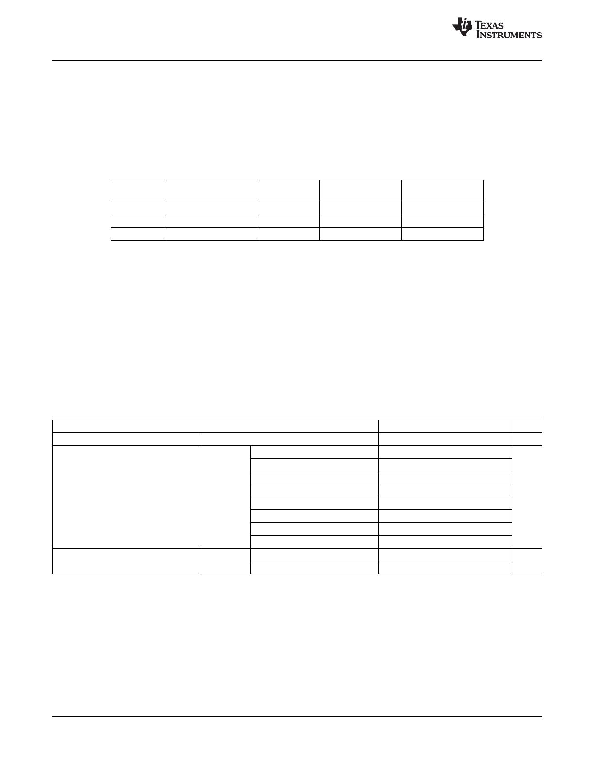
Page 8
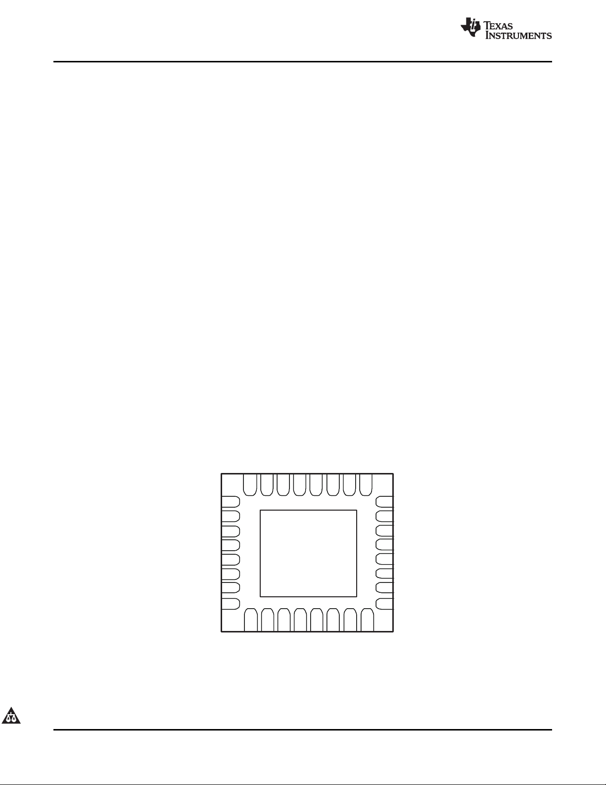
V
DDIO
DIR
V
DD18
STP
V
DD18
RESETB
CLOCK
N/C
32
31
30
29
28
27
26
25
REFCLK 1
24
N/C
NXT 2
23
ID
DATA0 3 TUSB1210
RHB PACKAGE
(TOP VIEW)
22
V
BUS
DATA1 4 32-pin QFN
21
V
BAT
DATA2 5
20
V
DD33
DATA3 6
19
DM
DATA4 7
GND
18
DP
N/C 8
17
CPEN
9
10
11
12
13
14
15
16
DATA5
DATA6
CS
V
DD15
DATA7
CFG
N/C
N/C
TUSB1210
www.ti.com
2 Description
The TUSB1210 is a USB2.0 transceiver chip, designed to interface with a USB controller via a ULPI
interface. It supports all USB2.0 data rates (High-Speed 480Mbps, Full-Speed 12 Mbps and Low-Speed
1.5Mbps) in both Host and Peripheral modes. It additionally supports a UART mode and legacy ULPI
serial modes.
TUSB1210 also supports the OTG (Ver1.3) optional addendum to the USB 2.0 Specification, including
Host Negotiation Protocol (HNP) and Session Request Protocol (SRP).
TUSB1210 is optimized to be interfaced through a 12-pin SDR UTMI Low Pin Interface (ULPI), supporting
both input clock and output clock modes, with 1.8 V interface supply voltage.
TUSB1210 integrates a 3.3 V LDO, which makes it flexible to work with either battery operated systems or
pure 3.3 V supplied systems. Both the main supply and the 3.3 V power domain can be supplied through
an external switched-mode converter for optimized power efficiency.
TUSB1210 includes a POR circuit to detect supply presence on V
disabled or configured in low power mode for energy saving.
TUSB1210 is protected against accidental shorts to 5 V or ground on its exposed interface (DP/DM/ID). It
is also protected against up to 20 V surges on V
TUSB1210 integrates a high-performance low-jitter 480 MHz PLL and supports two clock configurations.
Depending on the required link configuration, TUSB1210 supports both ULPI input and output clock mode
: input clock mode, in which case a square-wave 60 MHz clock is provided to TUSB1210 at the ULPI
interface CLOCK pin; and output clock mode in which case TUSB1210 can accept a square-wave
reference clock at REFCLK of either 19.2 MHz, 26 MHz. Frequency is indicated to TUSB1210 via the
configuration pin CFG. This can be useful if a reference clock is already available in the system.
BUS
SLLSE09D–NOVEMBER 2009–REVISED JANUARY 2011
BAT
and V
pins. TUSB1210 can be
DDIO
.
1
2.1 Terminal Description
1
Please be aware that an important notice concerning availability, standard warranty, and use in critical applications of Texas
Instruments semiconductor products and disclaimers thereto appears at the end of this data sheet.
Copyright © 2009–2011, Texas Instruments Incorporated
PRODUCTION DATA information is current as of publication date.
Products conform to specifications per the terms of the Texas
Instruments standard warranty. Production processing does not
necessarily include testing of all parameters.
Page 9
TUSB1210
www.ti.com
SLLSE09D–NOVEMBER 2009–REVISED JANUARY 2011
Table 2-1. Terminal Functions
TERMINAL
NO. NAME
1 REFCLK A I 3.3 V clock of amplitude in the range of 3 V to 3.6 V when Pin 26 (CLOCK) is
2 NXT D O V
3 DATA0 D I/O V
4 DATA1 D I/O V
5 DATA2 D I/O V
6 DATA3 D I/O V
7 DATA4 D I/O V
8 N/C – – V
9 DATA5 D I/O V
10 DATA6 D I/O V
11 CS D I V
12 VDD15 A power 1.5-V internal LDO output. Connect to external filtering capacitor.
13 DATA7 D I/O V
14 CFG D I V
15 N/C – – – No connect
16 N/C – – – No connect
17 CPEN D O V
18 DP A I/O V
19 DM A I/O V
20 V
21 V
22 V
DD33
BAT
BUS
23 ID A I/O V
24 N/C – – – No connect
25 N/C – – – No connect
26 CLOCK D O V
27 RESETB D I V
28 V
DD18
29 STP D I V
30 V
DD18
31 DIR D O V
32 V
DDIO
A/D TYPE LEVEL DESCRIPTION
V
Reference clock input (square-wave only). Tie to GND when pin 26
DD33
(CLOCK) is required to be Input mode. Connect to square-wave reference
required to be Output mode. See pin 14 (CFG) description for REFCLK
input frequency settings.
ULPI NXT output signal
ULPI DATA input/output signal 0 synchronized to CLOCK
ULPI DATA input/output signal 1 synchronized to CLOCK
ULPI DATA input/output signal 2 synchronized to CLOCK
ULPI DATA input/output signal 3 synchronized to CLOCK
ULPI DATA input/output signal 4 synchronized to CLOCK
No connect
ULPI DATA input/output signal 5 synchronized to CLOCK
ULPI DATA input/output signal 6 synchronized to CLOCK
Active-high chip select pin. When low the IC is in power down and ULPI
bus is tri-stated. When high normal operation. Tie to V
ULPI DATA input/output signal 7 synchronized to CLOCK
REFCLK clock frequency configuration pin. Two frequencies are
supported: 19.2 MHz when 0, or 26 MHz when 1.
CMOS active-high digital output control of external 5V VBUS supply
DP pin of the USB connector
DM pin of the USB connector
3.3-V internal LDO output. Connect to external filtering capacitor.
Input supply voltage or battery source
BAT
V
BUS
pin of the USB connector
BUS
Identification (ID) pin of the USB connector
A power V
A power V
A power V
DDIO
DDIO
DDIO
DDIO
DDIO
DDIO
DDIO
DDIO
DDIO
DDIO
DDIO
DDIO
DD33
DD33
DD33
DD33
DD33
ULPI 60 MHz clock on which ULPI data is synchronized.
Two modes are possible:
DDIO
Input Mode: CLOCK defaults as an input.
Output Mode: When an input clock is detected on REFCLK pin (after 4
rising edges) then CLOCK will change to an output.
When low, all digital logic (except 32 kHz logic required for power up
sequencing) including registers are reset to their default values, and ULPI
bus is tri-stated. When high, normal USB operation.
External 1.8-V supply input. Connect to external filtering capacitor.
ULPI STP input signal
External 1.8-V supply input. Connect to external filtering capacitor.
ULPI DIR output signal
External 1.8V supply input for digital I/Os. Connect to external filtering
capacitor.
A power V
A power V
A I V
DDIO
DD18
DDIO
DD18
DDIO
DDIO
DDIO
if unused.
Copyright © 2009–2011, Texas Instruments Incorporated Description 9
Submit Documentation Feedback
Product Folder Link(s): TUSB1210
Page 10
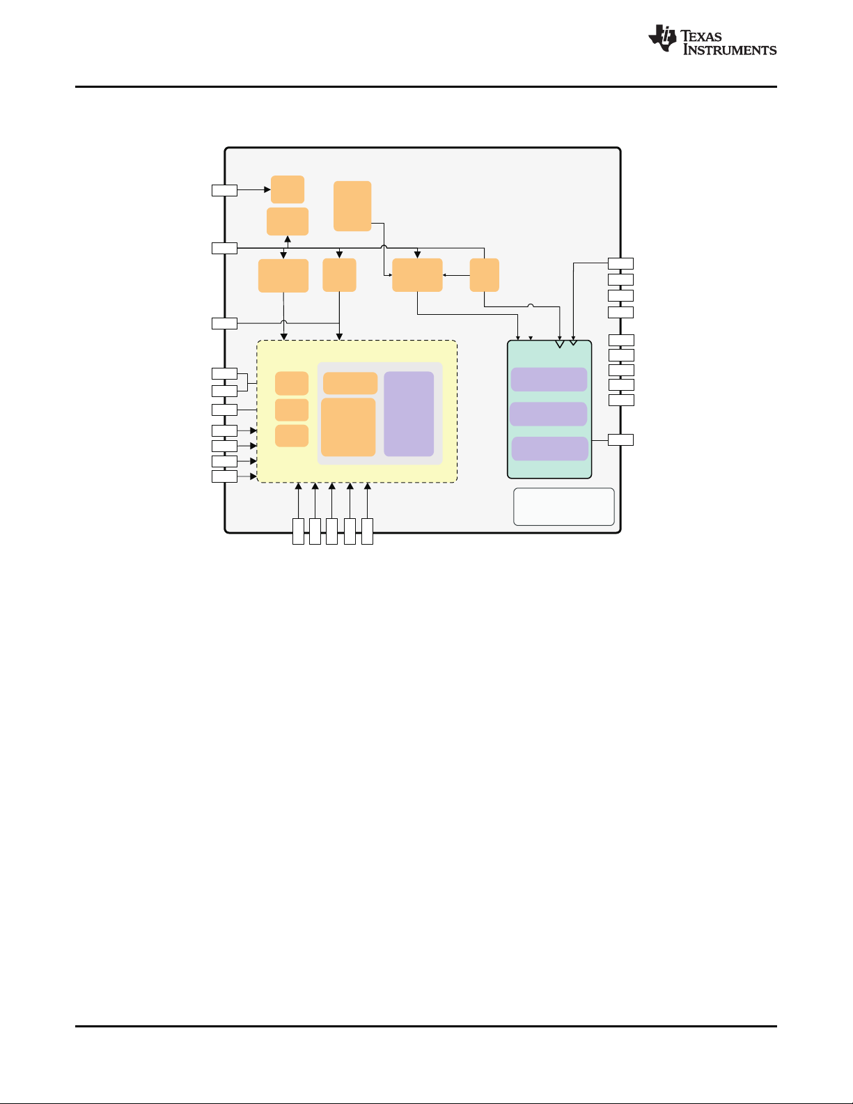
USB-IP
OTG
1V5
3V3
1V8
POR
VBAT
PLL
PHY
ANA
PHY
DIG
+
ULPI
+
REGS
32K
BGAP
& REF
POR
DIG
DIG
TEST
OTG
PWR_ FSM
POR
VIO
CTRL
RST_DIG
VDDIO (32)
VBAT (21)
N/
C
(24)
VDD15 (12)
VDD18 (28)
VDD33 (20)
DP (18)
DM (19)
ID (23)
(22)
VBUS
( 1) REFCLK
(25)
N/
C
(17) CPEN
(3:7,9:10,13)
DATA (7:0)
(2 ) NXT
(31) DIR
(29) STP
(26) CL OCK
(16)
N/
C
(15)
N/
C
VDD18 (30)
PKG Substrate
(Ground )
(14) CFG
(11) CS
(8)
N/
C
(27) RESETB
TUSB1210
SLLSE09D–NOVEMBER 2009–REVISED JANUARY 2011
2.2 TUSB1210 Block Diagram
www.ti.com
10 Description Copyright © 2009–2011, Texas Instruments Incorporated
Submit Documentation Feedback
Product Folder Link(s): TUSB1210
Page 11
TUSB1210
www.ti.com
SLLSE09D–NOVEMBER 2009–REVISED JANUARY 2011
3 Electrical Characteristics
3.1 Absolute Maximum Ratings
over operating free-air temperature range (unless otherwise noted)
PARAMETER CONDITIONS MIN MAX UNIT
V
CC
Main battery supply voltage
Voltage on any input
V
input –2 20 V
BUS
ID, DP, DM inputs Stress condition guaranteed 24h –0.3 5.25 V
V
T
T
T
DDIO
stg
A
J
IO supply voltage Continuous 1.98 V
Storage temperature range –55 125 °C
Ambient temperature range –40 85 °C
Ambient temperature range °C
Ambient temperature for parametric With max 125°C as junction temperature
compliance
DP, DM, ID high voltage short circuit supply, in any mode of TUSB1210 operation, 5.25 V
DP, DM, ID low voltage short circuit any mode of TUSB1210 operation, 0 V
(1) Stresses beyond those listed under “absolute maximum ratings” may cause permanent damage to the device. These are stress ratings
only, and functional operation of the device at these or any other conditions beyond those indicated under “recommended operating
conditions” is not implied. Exposure to absolute-maximum-rated conditions for extended periods may affect device reliability.
(2) The product will have negligible reliability impact if voltage spikes of 5.5 V occur for a total (cumulative over lifetime) duration of 5
milliseconds.
(3) Except V
BAT
input, V
, ID, DP, and DM pads
BUS
(2)
(3)
Where supply represents the voltage applied
to the power supply pin associated with the –0.3 1 × VCC+0.3 V
input
Absolute maximum rating –40 150
For parametric compliance –40 125
DP, DM or ID pins short circuited to V
continuously for 24 hours
DP, DM or ID pins short circuited to GND in
continuously for 24 hours
(1)
0 5 V
–40 85 °C
BUS
3.2 Recommended Operating Conditions
over operating free-air temperature range (unless otherwise noted)
PARAMETER TEST CONDITIONS MIN NOM MAX UNIT
V
BAT
V
BAT
CERT
V
DDIO
T
A
Battery supply voltage 2.7 3.6 4.8 V
Battery supply voltage for USB 2.0 compliancy
(USB 2.0 certification)
When V
When V
is supplied internally 3.15 V
DD33
is shorted to V
DD33
externally 3.05
BAT
Digital IO pin supply 1.71 1.98 V
Ambient temperature range –40 85 °C
3.3 ESD Electrical Parameters
over operating free-air temperature range (unless otherwise noted)
PARAMETER TEST CONDITIONS MIN TYP MAX UNIT
CDM Charged-Device Model stress voltage All pads 500 V
HBM Human-Body Model stress voltage All pads 2000 V
Copyright © 2009–2011, Texas Instruments Incorporated Electrical Characteristics 11
Submit Documentation Feedback
Product Folder Link(s): TUSB1210
Page 12
TUSB1210
SLLSE09D–NOVEMBER 2009–REVISED JANUARY 2011
4 Clock System
4.1 USB PLL Reference Clock
The USB PLL block generates the clocks used to synchronize :
• the ULPI interface (60 MHz clock)
• the USB interface (depending on the USB data rate, 480 Mbps, 12 Mbps or 1.5 Mbps)
TUSB1210 requires an external reference clock which is used as an input to the 480 MHz USB PLL block.
Depending on the clock configuration, this reference clock can be provided either at REFCLK pin or at
CLOCK pin. By default CLK pin is configured as an input.
Two clock configurations are possible:
• Input clock configuration (see Section 4.2)
• Output clock configuration (see Section 4.3)
4.2 ULPI Input Clock Configuration
In this mode REFCLK must be externally tied to GND. CLOCK remains configured as an input.
When the ULPI interface is used in “input clock configuration”, i.e., the 60 MHz ULPI clock is provided to
TUSB1210 on Clock pin, then this is used as the reference clock for the 480 MHz USB PLL block.
Table 4-1. Electrical Characteristics: Clock Input
www.ti.com
PARAMETER TEST CONDITIONS MIN TYP MAX UNIT
Clock input duty cycle 40 60 %
f
CLK
Clock nominal frequency 60 MHz
Clock input rise/fall time In % of clock period t
Clock input frequency accuracy 250 ppm
Clock input integrated jitter 600 ps rms
4.3 ULPI Output Clock Configuration
In this mode a reference clock must be externally provided on REFCLK pin When an input clock is
detected on REFCLK pin then CLK will automatically change to an output, i.e., 60 MHz ULPI clock is
output by TUSB1210 on CLK pin.
Two reference clock input frequencies are supported. REFCLK input frequency is communicated to
TUSB1210 via a configuration pin, CFG, see f
TUSB1210 supports square-wave reference clock input only. Reference clock input must be square-wave
of amplitude in the range 3.0 V to 3.6 V.
Table 4-2. Electrical Characteristics: REFCLK
PARAMETER TEST CONDITIONS MIN TYP MAX UNIT
REFCLK input duty cycle 40 60 %
f
REFCLK
REFCLK nominal frequency MHz
REFCLK input rise/fall time 20 %
REFCLK input frequency accuracy 250 ppm
REFCLK input integrated jitter 600 ps rms
When CFG pin is tied to GND 19.2
When CFG pin is tied to V
In % of clock period t
1/f
REFCLK
( = 1/f
CLK
REFCLK
DDIO
)
REFCLK
) 10 %
CLK
in Table 8-1 for frequency correspondence.
26
( =
12 Clock System Copyright © 2009–2011, Texas Instruments Incorporated
Submit Documentation Feedback
Product Folder Link(s): TUSB1210
Page 13
TUSB1210
www.ti.com
SLLSE09D–NOVEMBER 2009–REVISED JANUARY 2011
4.4 Clock 32 kHz
An internal clock generator running at 32 kHz has been implemented to provide a low-speed, low-power
clock to the system
Table 4-3. Performances
PARAMETER TEST CONDITIONS MIN TYP MAX UNIT
Output duty cycle Input duty cycle 40–60% 48 50 52 %
Output frequency 23 32 38 kHz
4.5 Reset
All logic is reset if CS = 0 or V
All logic (except 32 kHz logic) is reset if V
PHY logic is reset when any supplies are not present (V
TUSB1210 may be reset manually by toggling the RESETB pin to GND for at lease 200 ns.
If manual reset via RESETB is not required then RESETB pin may be tied to V
are not present.
BAT
is not present.
DDIO
DDIO
, V
DD15
, V
DD18
, V
) or if RESETB pin is low.
DD33
permanently.
DDIO
Copyright © 2009–2011, Texas Instruments Incorporated Clock System 13
Submit Documentation Feedback
Product Folder Link(s): TUSB1210
Page 14
TUSB1210
SLLSE09D–NOVEMBER 2009–REVISED JANUARY 2011
5 Power Module
This chapter describes the electrical characteristics of the voltage regulators and timing characteristics of
the supplies digitally controlled within the TUSB1210.
5.1 Power Providers
Table 5-1. Summary of TUSB1210 Power Providers
NAME USAGE TYPE
5.1.1 V
The V
subchip inside TUSB1210. Table 5-2 describes the regulator characteristics.
(1) V
Regulator
DD33
DD33
V
DD15
V
DD18
V
DD33
may be supplied externally, or by shorting the V
DD33
range [3.2 V : 3.6 V]. Note that the V
irrespective of whether V
externally in the application, the electrical specs for this LDO are provided below.
internal LDO regulator powers the USB PHY, charger detection, and OTG functions of the USB
Internal LDO 1.5 50
External LDO 1.8 30
Internal LDO 3.1 15
DD33
TYPICAL MAXIMUM
VOLTAGE (V) CURRENT (mA)
pin to V
LDO will always power-on when the chip is enabled,
DD33
is supplied externally or not. In the case the V
DD33
pin provided V
BAT
(1)
BAT
pin is not supplied
DD33
www.ti.com
min is in
V
Since the USB2.0 standard requires data lines to be biased with pullups biased from a supply greater than
3 V, and since V
TUSB1210 will not meet USB 2.0 Standard if operated from a battery whose voltage is lower than 3.3 V.
V
INVDD33
V
VDD33
I
VDD33
5.1.2 V
The V
regulator takes its power from V
DD33
regulator has an inherent voltage drop from its input, V
DD33
Table 5-2. V
PARAMETER TEST CONDITIONS MIN TYP MAX UNIT
Input voltage V
Output voltage ON mode, V
Rated output current V
Supply
DD18
supply is powered externally at the V
DD18
DD33
USB V
BAT
USB mA
BAT
.
BAT
, to its regulated output,
BAT
Internal LDO Regulator Characteristics
typ + 0.2 3.6 4.5 V
VDD33
VUSB3V3_VSEL = ‘000 2.4 2.5 2.6
VUSB3V3_VSEL = ‘001 2.65 2.75 2.85
VUSB3V3_VSEL = ‘010 2.9 3.0 3.1
VUSB3V3_VSEL = ‘011 (default) 3.0 3.1 3.2
VUSB3V3_VSEL = ‘100 3.1 3.2 3.3
VUSB3V3_VSEL = ‘101 3.2 3.3 3.4
VUSB3V3_VSEL = ‘110 3.3 3.4 3.5
VUSB3V3_VSEL = ‘111 3.4 3.5 3.6
Active mode 15
Suspend/reset mode 1
pin. See Table 8-1 for external components.
DD18
5.1.3 V
The V
Regulator
DD15
DD15
internal LDO regulator powers the USB subchip inside TUSB1210. Table 5-3 describes the
regulator characteristics.
14 Power Module Copyright © 2009–2011, Texas Instruments Incorporated
Submit Documentation Feedback
Product Folder Link(s): TUSB1210
Page 15
TUSB1210
www.ti.com
Table 5-3. V
Internal LDO Regulator Characteristics
DD15
SLLSE09D–NOVEMBER 2009–REVISED JANUARY 2011
PARAMETER TEST CONDITIONS MIN TYP MAX UNIT
V
IN VDD15
V
VDD15
I
VDD15
Input voltage On mode, V
Output voltage V
INVDD15 min
IN VDD15
– V
INVDD15 max
= V
BAT
2.7 3.6 4.5 V
1.45 1.56 1.65 V
Rated output current On mode 30 mA
5.2 Power Consumption
Table 5-4 describes the power consumption depending on the use cases.
NOTE
The typical power consumption is obtained in the nominal operating conditions and with the
TUSB1210 standalone.
Table 5-4. Power Consumption
MODE CONDITIONS SUPPLY UNIT
I
VBAT
I
V
= 3.6 V, V
OFF Mode µA
Suspend Mode µA
HS USB Operation V
(Synchronous Mode) = 1.8 V, active USB transfer
FS USB Operation V
(Synchronous Mode) USB transfer
Reset Mode µA
BAT
= 1.8 V, CS = 0 V
V
= 5 V, V
BUS
1.8 V, No clock
= 3.6 V, V
BAT
= 3.6 V, V
BAT
RESETB = 0 V, V
= 3.6 V, V
DDIO
= 1.8 V, V
DDIO
= 3.6 V, V
BAT
= 1.8 V, V
DDIO
= 1.8 V, active
DDIO
= 5 V, V
BUS
= 1.8 V, No clock
DDIO
DD18
=
DD18
BAT
VDDIO
I
VDD18
I
TOTAL
I
VBAT
I
VDDIO
I
VDD18
I
TOTAL
I
VBAT
I
VDDIO
I
VDD18
I
TOTAL
I
VBAT
I
VDDIO
I
VDD18
I
TOTAL
I
VBAT
I
VDDIO
I
VDD18
I
TOTAL
TYPICAL
CONSUMPTION
8
3
5
16
204
3
3
210
24.6
1.89
21.5
48
25.8
1.81
4.06
31.7
237
3
3
243
mA
mA
Copyright © 2009–2011, Texas Instruments Incorporated Power Module 15
Submit Documentation Feedback
Product Folder Link(s): TUSB1210
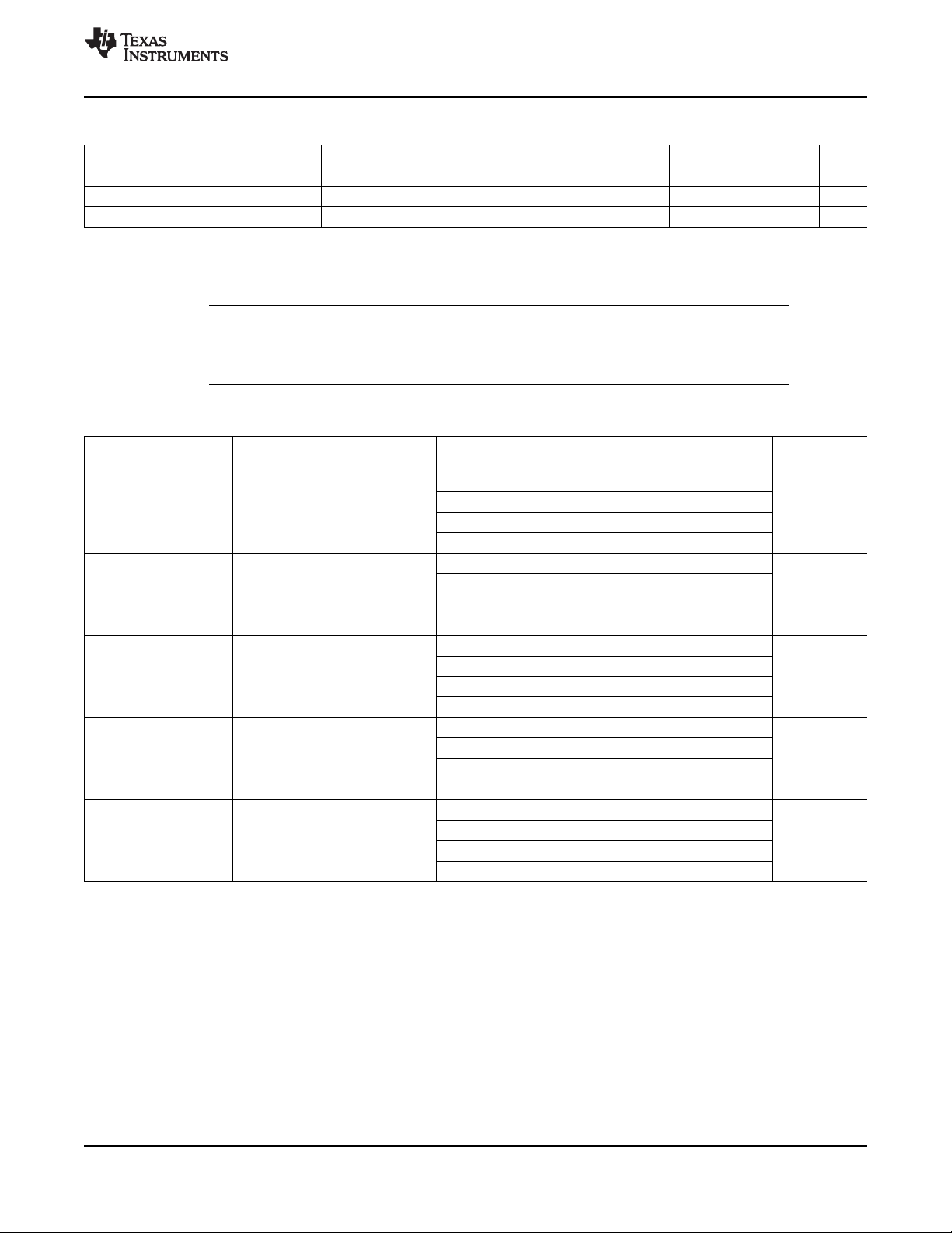
Page 16
VBAT , VDD33
VDDIO, VDD18
IORST
CS
ICACT
VDD15
DIGPOR
CK32K
BGOK
CK32KOK
MNTR_(VDD18,VIO)_OK
MNTR_VDD33_OK
RESETN_PWR
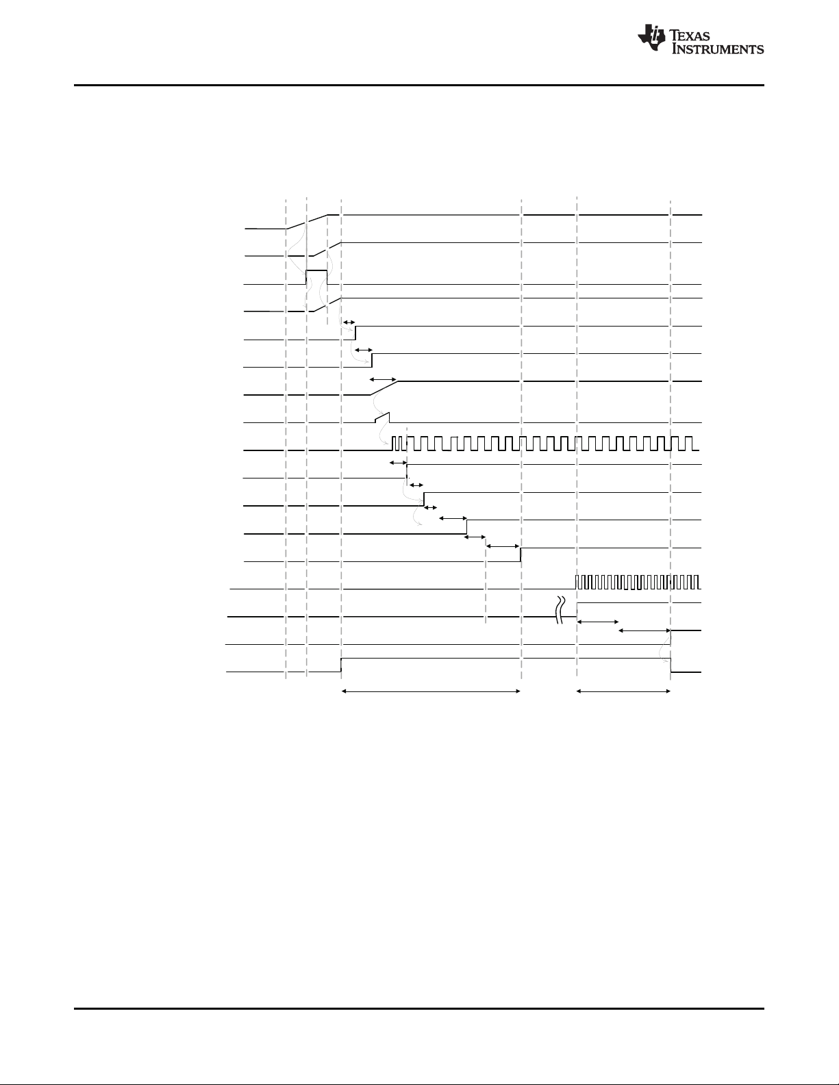
TDELRSTPWR (61us)
TDELMNTRVIOEN (91.5us)
TDELVDD33EN (91.5us)
TMNTR (183.1us)
(input 60M) CLOCK
PLL 480M LOCKED
TPLL (300us)
DIR
TBGAP (2ms)
TPWONVDD15 (100us)
RESETB
TDELRESETB (244.1us)
TVBBDET (10us)
TCK32K_PWON (125us)
TMNTR (183.1us)
TDEL_CS_SUPPLYOK (2.84ms)
TDEL_RST_DIR (0.54ms)
NOPWR
OFF
HWRST
COLDRST
ACTIVE
TUSB1210
SLLSE09D–NOVEMBER 2009–REVISED JANUARY 2011
5.3 Power Management
5.3.1 Power On Sequence
5.3.1.1 Timing Diagram
www.ti.com
Figure 5-1. TUSB1210 Power-Up Timing (ULPI Clock Input Mode)
16 Power Module Copyright © 2009–2011, Texas Instruments Incorporated
Submit Documentation Feedback
Product Folder Link(s): TUSB1210
Page 17
TUSB1210
www.ti.com
5.3.2 Timers and Debounce
PARAMETER COMMENTS MIN TYP MAX UNIT
T
DEL_CS_SUPPLYOK
T
DEL_RST_DIR
T
VBBDET
T
BGAP
T
PWONVDD15
T
PWONCK32K
T
DELRSTPWR
T
DELMNTRVIOEN
T
MNTR
T
DELVDD33EN
T
DELRESETB
T
PLL
Chip-select-to-supplies OK delay 2.84 4.10 ms
RESETB to PHY PLL locked and DIR 0.54 0.647 ms
falling-edge delay
V
detection delay 10 us
BAT
Bandgap power-on delay 2 ms
V
power-on delay 100 us
DD15
32-KHz RC-OSC power-on delay 125 us
Power control reset delay 61 us
Monitor enable delay 91.5 us
Supply monitoring debounce 183.1 us
V
LDO enable delay 93.75 us
DD33
RESETB internal delay 244.1 us
PLL lock time 300 us
SLLSE09D–NOVEMBER 2009–REVISED JANUARY 2011
Copyright © 2009–2011, Texas Instruments Incorporated Power Module 17
Submit Documentation Feedback
Product Folder Link(s): TUSB1210
Page 18
TUSB1210
SLLSE09D–NOVEMBER 2009–REVISED JANUARY 2011
6 USB Connectivity
6.1 Timing Parameter Definitions
The timing parameter symbols used in the timing requirement and switching characteristic tables are
created in accordance with JEDEC Standard 100. To shorten the symbols, some pin names and other
related terminologies have been abbreviated as shown in Table 6-1.
Table 6-1. Timing Parameter Definitions
SYMBOL PARAMETER
C Cycle time (period)
D Delay time
Dis Disable time
En Enable time
H Hold time
Su Setup time
START Start bit
T Transition time
V Valid time
W Pulse duration (width)
X Unknown, changing, or don't care level
H High
L Low
V Valid
IV Invalid
AE Active edge
FE First edge
LE Last edge
Z High impedance
www.ti.com
LOWERCASE SUBSCRIPTS
6.2 Interface Target Frequencies
Table Table 6-2 assumes testing over the recommended operating conditions.
Table 6-2. TUSB1210 Interface Target Frequencies
IO INTERFACE DESIGNATION TARGET
INTERFACE FREQUENCY
USB Universal High speed 480 Mbits/s
serial bus
Full speed 12 Mbits/s
Low speed 1.5 Mbits/s
1.5 V
6.3 USB Transceiver
The TUSB1210 device includes a universal serial bus (USB) on-the-go (OTG) transceiver that supports
USB 480 Mb/s high-speed (HS), 12 Mb/s full-speed (FS), and USB 1.5 Mb/s low-speed (LS) through a
12-pin UTMI+ low pin interface (ULPI).
18 USB Connectivity Copyright © 2009–2011, Texas Instruments Incorporated
Submit Documentation Feedback
Product Folder Link(s): TUSB1210
Page 19

TUSB1210
www.ti.com
SLLSE09D–NOVEMBER 2009–REVISED JANUARY 2011
6.3.1 TUSB1210 Modes vs ULPI Pin Status
Table 6-3, Table 6-4, and Table 6-5 show the status of each of the 12 ULPI pins including input/output
direction and whether output pins are driven to ‘0’ or to ‘1’, or pulled up/pulled down via internal
pullup/pulldown resistors.
Note that pullup/pulldown resistors are automatically replaced by driven ‘1’/’0’ levels respectively once
internal IORST is released, with the exception of the pullup on STP which is maintained in all modes.
Pin assignment changes in ULPI 3-pin serial mode, ULPI 6-pin serial mode, and UART mode. Unused
pins are tied low in these modes as shown below.
Table 6-3. TUSB1210 Modes vs ULPI Pin Status:ULPI Synchronous Mode Power-Up
ULPI SYNCHRONOUS MODE POWER-UP
UNTIL IORST RELEASE PLL OFF PLL ON + STP HIGH PLL ON + STP LOW
PIN
NO.
PIN NAME DIR PU/PD DIR PU/PD DIR PU/PD DIR PU/PD
26 CLOCK Hiz PD I PD IO - IO 31 DIR Hiz PU O, (‘1’) - O, (‘0’) - O -
2 NXT Hiz PD O, (‘0’) - O, (‘0’) - O -
29 STP Hiz PU I PU I PU I PU
3 DATA0 Hiz PD O, (‘0’) - I PD IO 4 DATA1 Hiz PD O, (‘0’) - I PD IO 5 DATA2 Hiz PD O, (‘0’) - I PD IO 6 DATA3 Hiz PD O, (‘0’) - I PD IO 7 DATA4 Hiz PD O, (‘0’) - I PD IO -
9 DATA5 Hiz PD O, (‘0’) - I PD IO 10 DATA6 Hiz PD O, (‘0’) - I PD IO 13 DATA7 Hiz PD O, (‘0’) - I PD IO -
Table 6-4. TUSB1210 Modes vs ULPI Pin Status: USB Suspend Mode
SUSPEND MODE
PIN NO. PIN NAME DIR PU/PD DIR PU/PD
26 CLOCK I - O 31 DIR O, (‘1’) - I -
2 NXT O, (‘0’) - I -
29 STP I PU
3 DATA0 O, - I -
(LINESTATE0)
4 DATA1 O, - I -
(LINESTATE1)
5 DATA2 O, (‘0’) - I 6 DATA3 O, (INT) - I 7 DATA4 O, (‘0’) - I 9 DATA5 O, (‘0’) - I -
10 DATA6 O, (‘0’) - I 13 DATA7 O, (‘0’) - I -
(1) Can be disabled by software before entering Suspend Mode to reduce current consumption
Copyright © 2009–2011, Texas Instruments Incorporated USB Connectivity 19
Submit Documentation Feedback
Product Folder Link(s): TUSB1210
(1)
LINK / EXTERNAL RECOMMENDED
SETTING DURING SUSPEND MODE
O, (‘0’) -
Page 20

TUSB1210
SLLSE09D–NOVEMBER 2009–REVISED JANUARY 2011
www.ti.com
Table 6-5. TUSB1210 Modes vs ULPI Pin Status: ULPI 6-Pin Serial Mode and UART Mode
ULPI 3-PIN SERIAL MODE UART MODE
PIN NO. PIN NAME DIR PU/PD PIN NAME DIR PU/PD PIN NAME DIR PU/PD
26 CLOCK (1) IO - CLOCK (1) IO - CLOCK (1) IO 31 DIR O - DIR O - DIR O -
2 NXT O - NXT O - NXT O -
29 STP I PU STP I PU STP I PU
3 TX_ENABLE I - TX_ENABLE I - TXD I 4 TX_DAT I - DAT IO - RXD IO 5 TX_SE0 I - SE0 IO - tie low O 6 INT O - INT O - INT O 7 RX_DP O - tie low O - tie low O -
9 RX_DM O - tie low O - tie low O 10 RX_RCV O - tie low O - tie low O 13 tie low O - tie low O - tie low O -
6.3.2 ULPI Interface Timing
Table 6-6. ULPI Interface Timing
INPUT CLOCK OUTPUT CLOCK
MIN MAX MIN MAX
TSC,T
TSC,T
TDC,T
SD
HD
DD
PARAMETER UNIT
Set-up time (control in, 8-bit data in) 3 6 ns
Hold time (control in, 8-bit data in) 1.5 0 ns
Output delay (control out, 8-bit data out) 6 9 ns
6.3.3 PHY Electrical Characteristics
The PHY is the physical signaling layer of the USB 2.0. It essentially contains all the drivers and receivers
required for physical data and protocol signaling on the DP and DM lines.
The PHY interfaces to the USB controller through a standard 12-pin digital interface called UTMI+ low pin
interface (ULPI).
The transmitters and receivers inside the PHY are classified into two main classes.
• The full-speed (FS) and low-speed (LS) transceivers. These are the legacy USB1.x transceivers.
• The HS (HS) transceivers
In order to bias the transistors and run the logic, the PHY also contains reference generation circuitry
which consists of:
• A DPLL which does a frequency multiplication to achieve the 480-MHz low-jitter lock necessary for
USB and also the clock required for the switched capacitor resistance block.
• A switched capacitor resistance block which is used to replicate an external resistor on chip.
Built-in pullup and pulldown resistors are used as part of the protocol signaling.
Apart from this, the PHY also contains circuitry which protects it from accidental 5-V short on the DP and
DM lines.
6.3.3.1 LS/FS Single-Ended Receivers
In addition to the differential receiver, there is a single-ended receiver (SE–, SE+) for each of the two data
lines D+/–. The main purpose of the single-ended receivers is to qualify the D+ and D– signals in the
full-speed/low-speed modes of operation.
20 USB Connectivity Copyright © 2009–2011, Texas Instruments Incorporated
Submit Documentation Feedback
Product Folder Link(s): TUSB1210
Page 21

TUSB1210
www.ti.com
SLLSE09D–NOVEMBER 2009–REVISED JANUARY 2011
Table 6-7. LS/FS Single-Ended Receivers
PARAMETER COMMENTS MIN TYP MAX UNIT
USB single-ended receivers
SK
WVP_VM
V
SE_HYS
V
IH
V
IL
V
TH
Skew between VP and VM Driver outputs unloaded –2 0 2 ns
Single-ended hysteresis 50 mV
High (driven) 2 V
Low 0.8 V
Switching threshold 0.8 2 V
6.3.3.2 LS/FS Differential Receiver
A differential input receiver (Rx) retrieves the LS/FS differential data signaling. The differential voltage on
the line is converted into digital data by a differential comparator on DP/DM. This data is then sent to a
clock and data recovery circuit which recovers the clock from the data. An additional serial mode exists in
which the differential data is directly output on the RXRCV pin.
Table 6-8. LS/FS Differential Receiver
PARAMETER COMMENTS MIN TYP MAX UNIT
VDIDifferential input sensitivity Ref. USB2.0 200 mV
VCMDifferential Common mode range Ref. USB2.0 0.8 2.5 V
6.3.3.3 LS/FS Transmitter
The USB transceiver (Tx) uses a differential output driver to drive the USB data signal D+/– onto the USB
cable. The driver's outputs support 3-state operation to achieve bidirectional half-duplex transactions.
PARAMETER COMMENTS MIN TYP MAX UNIT
V
OL
V
OH
V
CRS
T
FR
T
FF
T
FRFM
T
FDRATE
T
DJ1
T
DJ2
T
FEOPT
V
CM
Low Ref. USB2.0 0 300 mV
High (driven) Ref. USB2.0 2.8 3.6 V
Output signal crossover voltage Ref. USB2.0, covered by 1.3 2 V
Rise time Ref. USB2.0, covered by 75 300 ns
Fall time 75 300 ns
Differential rise and fall time matching 80 125 %
Low-speed data rate Ref. USB2.0, covered by 1.4775 1.5225 Mb/s
Source jitter total (including To next transition Ref. USB2.0, covered by -25 25 ns
frequency tolerance) eye diagram
Source SE0 interval of EOP Ref. USB2.0, covered by 1.25 1.5 us
Downstream eye diagram Ref. USB2.0, covered by
Differential common mode range Ref. USB2.0 0.8 2.5 V
Table 6-9. LS Transmitter
eye diagram
eye diagram
eye diagram
For paired transitions -10 10
eye diagram
eye diagram
Copyright © 2009–2011, Texas Instruments Incorporated USB Connectivity 21
Submit Documentation Feedback
Product Folder Link(s): TUSB1210
Page 22

TUSB1210
SLLSE09D–NOVEMBER 2009–REVISED JANUARY 2011
www.ti.com
Table 6-10. FS Transmitter
PARAMETER COMMENTS MIN TYP MAX UNIT
V
OL
V
OH
VCRS Output signal crossover voltage
t
FR
t
FF
t
FRFM
Z
DRV
TFDRATE Full-speed data rate Ref. USB2.0, covered by eye 11.97 12.03 Mb/s
T
DJ1
T
DJ2
TFEOPT Source SE0 interval of EOP Ref. USB2.0, covered by eye 160 175 ns
Low Ref. USB2.0 0 300 mV
High (driven) Ref. USB2.0 2.8 3.6 V
Ref. USB2.0, covered by eye 1.3 2 V
diagram
Rise time Ref. USB2.0 4 20 ns
Fall time Ref. USB2.0 4 20 ns
Differential rise and fall time matching Ref. USB2.0, covered by eye 90 111.1 %
Driver output resistance Ref. USB2.0 28 44 Ω
Source jitter total (including
frequency tolerance)
Downstream eye diagram Ref. USB2.0, covered by eye
Upstream eye diagram
To next transition Ref. USB2.0, covered by eye -2 2 ns
For paired transitions -1 1
diagram 1
diagram
diagram
diagram
diagram
6.3.3.4 HS Differential Receiver
The HS receiver consists of the following blocks:
A differential input comparator to receive the serial data
• A squelch detector to qualify the received data
• An oversampler-based clock data recovery scheme followed by a NRZI decoder, bit unstuffing, and
serial-to-parallel converter to generate the ULPI DATAOUT
Table 6-11. HS Differential Receiver
PARAMETER COMMENTS MIN TYP MAX UNIT
VHSSQ High-speed squelch detection threshold Ref. USB2.0 100 150 mV
VHSDSC High-speed disconnect detection threshold Ref. USB2.0 525 625 mV
VHSCM High-speed data signaling common mode Ref. USB2.0 -50 500 mV
(differential signal amplitude)
(differential signal amplitude)
High-speed differential input signaling levels Ref. USB2.0, specified by eye pattern mV
templates
voltage range (guidelines for receiver)
Receiver jitter tolerance Ref. USB2.0, specified by eye pattern 150 ps
templates
6.3.3.5 HS Differential Transmitter
The HS transmitter is always operated via the ULPI parallel interface. The parallel data on the interface is
serialized, bit stuffed, NRZI encoded, and transmitted as a dc output current on DP or DM depending on
the data. Each line has an effective 22.5-Ω load to ground, which generates the voltage levels for
signaling.
A disconnect detector is also part of the HS transmitter. A disconnect on the far end of the cable causes
the impedance seen by the transmitter to double thereby doubling the differential amplitude seen on the
DP/DM lines.
22 USB Connectivity Copyright © 2009–2011, Texas Instruments Incorporated
Submit Documentation Feedback
Product Folder Link(s): TUSB1210
Page 23

TUSB1210
www.ti.com
SLLSE09D–NOVEMBER 2009–REVISED JANUARY 2011
Table 6-12. HS Transmitter
PARAMETER COMMENTS MIN TYP MAX UNIT
V
V
V
HSOI
HSOH
HSOL
High-speed idle level Ref. USB2.0 -10 10 mV
High-speed data signaling high Ref. USB2.0 360 440 mV
High-speed data signaling low Ref. USB2.0 -10 10 mV
VCHIRPJ Chirp J level (differential voltage) Ref. USB2.0 700 1100 mV
VCHIRPK Chirp K level (differential voltage) Ref. USB2.0 -900 -500 mV
THSR Rise Time (10% - 90%) Ref. USB2.0, covered by eye diagram 500 ps
THSR Fall time (10% - 90%) Ref. USB2.0, covered by eye diagram 500 ps
ZHSDRV Driver output resistance (which also serves as Ref. USB2.0 40.5 49.5 Ω
high-speed termination)
THSDRAT High-speed data range Ref. USB2.0, covered by eye diagram 479.76 480. Mb/s
24
Data source jitter Ref. USB2.0, covered by eye diagram
Downstream eye diagram Ref. USB2.0, covered by eye diagram
Upstream eye diagram Ref. USB2.0, covered by eye diagram
6.3.3.6 UART Transceiver
In this mode, the ULPI data bus is redefined as a 2-pin UART interface, which exchanges data through a
direct access to the FS/LS analog transmitter and receiver.
t
PH_DP_CON
t
PH_DISC_DET
f
UART_DFLT
t
PH_UART_EDGE
V
OH_SER
V
OL_SER
VI
H_SER
V
IL_SER
V
TH
Table 6-13. USB UART Interface Timing Parameters
PARAMETER MIN MAX UNIT
Phone D+ connect time 100 ms
Phone D+ disconnect time 150 ms
Default UART signaling rate (typical rate) 9600 bps
Figure 6-1. USB UART Data Flow
Table 6-14. CEA-2011/UART Transceiver
PARAMETER COMMENTS MIN TYP MAX UNIT
UART Transmitter CEA-2011
Phone UART edge rates DP_PULLDOWN asserted 1 Μs
Serial interface output high ISOURCE = 4 mA 2.4 3.3 3.6 V
Serial interface output low ISINK = –4 mA 0 0.1 0.4 V
UART Receiver CEA-2011
Serial interface input high DP_PULLDOWN asserted 2 V
Serial interface input low DP_PULLDOWN asserted 0.8 V
Switching threshold 0.8 2 V
Copyright © 2009–2011, Texas Instruments Incorporated USB Connectivity 23
Submit Documentation Feedback
Product Folder Link(s): TUSB1210
Page 24

TUSB1210
SLLSE09D–NOVEMBER 2009–REVISED JANUARY 2011
www.ti.com
Table 6-15. Pullup/Pulldown Resistors
PARAMETER COMMENTS MIN TYP MAX UNIT
RPUI
RPUA
VIHZ
Bus pullup resistor on upstream port Bus idle 0.9 1.1 1.575 kΩ
(idle bus)
Bus pullup resistor on upstream port Bus driven/driver's outputs unloaded 1.425 2.2 3.09
(receiving)
High (floating) Pullups/pulldowns on both DP and 2.7 3.6 V
DM lines
VPH_DP_UP Phone D+ pullup voltage Driver's outputs unloaded 3 3.3 3.6 V
Pulldown resistors
RPH_DP_DWN Phone D+/– pulldown Driver's outputs unloaded 14.25 18 24.8 kΩ
RPH_DM_DWN
VIHZ
High (floating) Pullups/pulldowns on both DP and 2.7 3.6 V
DM lines
D+/– Data line
CINUB Upstream facing port [1.0] 22 75 pF
VOTG_DATA_LK On-the-go device leakage
G
ZINP
Input impedance exclusive of Driver's outputs unloaded 300 kΩ
pullup/pulldown
[2] 0.342 V
6.3.4 OTG Electrical Characteristics
The on-the-go (OTG) block integrates three main functions:
• The USB plug detection function on V
BUS
and ID
• The ID resistor detection
• The V
V
Comparators
BUS
VA_SESS_VLD A-device session valid 0.8 1.1 1.4 V
VA_VBUS_VLD A-device V
VB_SESS_END B-device session end 0.2 0.5 0.8 V
VB_SESS_VLD B-device session valid 2.1 2.4 2.7 V
V
Line
BUS
RA_BUS_IN A-device V
RB_SRP_DWN B-device V
RB_SRP_UP B-device V
t
RISE_SRP_UP_MAX
t
RISE_SRP_UP_MIN
level detection
BUS
Table 6-16. OTG V
Electrical
BUS
PARAMETER COMMENTS MIN TYP MAX UNIT
valid 4.4 4.5 4.625 V
BUS
input impedance to SRP (V
ground driving V
B-device V
maximum for OTG-A communication
B-device V
minimum for standard host TBD ms
BUS
SRP pulldown 5.25 V / 8 mA, Pullup voltage = 3 V 0.656 10 kΩ
BUS
SRP pullup (5.25 V – 3 V) / 8 mA, Pullup voltage = 3 V 0.281 1 2 kΩ
BUS
SRP rise time
BUS
SRP rise time 0.8 to 2.0 V with > 97 mF load
BUS
0 to 2.1 V with < 13 mF load TBD ms
pulsing) capable A-device not
BUS
BUS
40 70 100 kΩ
connection
24 USB Connectivity Copyright © 2009–2011, Texas Instruments Incorporated
Submit Documentation Feedback
Product Folder Link(s): TUSB1210
Page 25

TUSB1210
www.ti.com
Table 6-17. OTG ID Electrical
PARAMETER COMMENTS MIN TYP MAX UNIT
ID Comparators — ID External Resistors Specifications
R
ID_GND
R
ID_FLOAT
R
PH_ID_UP
VP
H_ID_UP
ID ground comparator ID_GND interrupt 12 20 28 kΩ
ID Float comparator ID_FLOAT interrupt 200 500 kΩ
ID Line
Phone ID pullup to VPH_ID_UP ID unloaded (V
Phone ID pullup voltage Connected to V
ID line maximum voltage 5.25 V
SLLSE09D–NOVEMBER 2009–REVISED JANUARY 2011
) 70 90 286 kΩ
RUSB
RUSB
2.5 3.2 V
Copyright © 2009–2011, Texas Instruments Incorporated USB Connectivity 25
Submit Documentation Feedback
Product Folder Link(s): TUSB1210
Page 26

TUSB1210
SLLSE09D–NOVEMBER 2009–REVISED JANUARY 2011
7 I/O Electrical Characteristics
7.1 Analog I/O Electrical Characteristics
Table 7-1. Electrical Characteristics: Analog Output Pins
PARAMETER CONDITIONS MIN TYP MAX UNIT
CPEN Output Pin
VOL
VOH
7.2 Digital I/O Electrical Characteristics
over operating free-air temperature range (unless otherwise noted)
NAME
CLOCK 0.45 V
STP 0.45 V
DIR 0.45 V
NXT 0.45 V
DATA0 0.45 V
DATA1 0.45 V
DATA2 0.45 V
DATA3 0.45 V
DATA4 0.45 V
DATA5 0.45 V
DATA6 0.45 V
DATA7 0.45 V
CPEN low-level output voltage IOL= 3 mA 0.3 V
CPEN
CPEN high-level output voltage IOH= -3 mA V
CPEN
VOL(V) VOH(V) VIL(V) VIH(V) MAX
PIN
MIN MAX MIN MAX MIN MAX MIN MAX
-0.45 0.35´V
DDIO
-0.45 0.35´V
DDIO
-0.45 0.35´V
DDIO
-0.45 0.35´V
DDIO
-0.45 0.35´V
DDIO
-0.45 0.35´V
DDIO
-0.45 0.35´V
DDIO
-0.45 0.35´V
DDIO
-0.45 0.35´V
DDIO
-0.45 0.35´V
DDIO
-0.45 0.35´V
DDIO
-0.45 0.35´V
DDIO
DDIO
DDIO
DDIO
DDIO
DDIO
DDIO
DDIO
DDIO
DDIO
DDIO
DDIO
DDIO
0.65´V
0.65´V
0.65´V
0.65´V
0.65´V
0.65´V
0.65´V
0.65´V
0.65´V
0.65´V
0.65´V
0.65´V
DDIO
DDIO
DDIO
DDIO
DDIO
DDIO
DDIO
DDIO
DDIO
DDIO
DDIO
DDIO
www.ti.com
-0.3 V
DD33
MAX LOAD MAX MAX
FREQ (pF) RISE TIME FALL TIME
(MHz) OUTPUT (ns) (ns)
MODE
60 10 1 1
30 10 1 1
30 10 1 1
30 10 1 1
30 10 1 1
30 10 1 1
30 10 1 1
30 10 1 1
30 10 1 1
30 10 1 1
30 10 1 1
30 10 1 1
7.3 Electrical Characteristics: Digital IO Pins (Non-ULPI)
over operating free-air temperature range (unless otherwise noted)
PARAMETER CONDITIONS MIN TYP MAX UNIT
CS, CFG, RESETB Input Pins
V
IL
V
IH
RESETB Input Pin Timing Spec
t
w(POR)
t
w(RESET)
Maximum low-level input voltage V
Minimum high-level input voltage 0.65*V
Internal power-on reset pulse
width
External RESETB pulse width 8
Applied to external RESETB pin when CLOCK
CLOCK is toggling. cycles
0.35 *
V
DDIO
DDIO
0.2 ms
V
26 I/O Electrical Characteristics Copyright © 2009–2011, Texas Instruments Incorporated
Submit Documentation Feedback
Product Folder Link(s): TUSB1210
Page 27

TUSB1210
www.ti.com
SLLSE09D–NOVEMBER 2009–REVISED JANUARY 2011
8 External Components
Table 8-1. TUSB1210 External Components
FUNCTION COMPONENT REFERENCE VALUE NOTE LINK
V
DDIO
V
DD33
V
DD15
V
DD18
V
BAT
V
BUS
(1) Recommended value but 2.2 uF may be sufficient in some applications
FUNCTION COMPONENT REFERENCE VALUE NOTE LINK
VBUS - HOST Capacitor CVBUS >120 mF Figure 10-1
VBUS – DEVICE Capacitor CVBUS 4.7 mF Range: 1.0 mF to 10.0 mF Figure 10-1
VBUS - OTG Capacitor CVBUS 4.7 mF Range: 1.0 mF to 6.5 mF Figure 10-1
Capacitor CVDDIO 100 nF Suggested value, application Figure 10-1
dependent
Capacitor CVDD33 2.2 mF Range: [0.45 mF : 6.5 mF] , Figure 10-1
ESR = [0 : 600 mΩ] for f> 10 kHz
Capacitor CVDD15 2.2 mF Range: [0.45 mF : 6.5 mF] , Figure 10-1
ESR = [0 : 600 mΩ] for f> 10 kHz
Capacitor Ext 1.8V supply 100 nF Suggested value, application Figure 10-1
CVDD18
Capacitor CBYP 100 nF
(1)
dependent
Range: [0.45 mF : 6.5 mF] , Figure 10-1
ESR = [0 : 600 mΩ] for f> 10 kHz
Capacitor CVBUS See table 1.2 Place close to USB connector Figure 10-1
Table 8-2. TUSB1210 V
Capacitors
BUS
Copyright © 2009–2011, Texas Instruments Incorporated External Components 27
Submit Documentation Feedback
Product Folder Link(s): TUSB1210
Page 28

TUSB1210
SLLSE09D–NOVEMBER 2009–REVISED JANUARY 2011
9 Register Map
9.1 TUSB1210 Product
Table 9-1. USB Register Summary
REGISTER NAME TYPE
VENDOR_ID_LO R 8 0x00
VENDOR_ID_HI R 8 0x01
PRODUCT_ID_LO R 8 0x02
PRODUCT_ID_HI R 8 0x03
FUNC_CTRL RW 8 0x04
FUNC_CTRL_SET RW 8 0x05
FUNC_CTRL_CLR RW 8 0x06
IFC_CTRL RW 8 0x07
IFC_CTRL_SET RW 8 0x08
IFC_CTRL_CLR RW 8 0x09
OTG_CTRL RW 8 0x0A
OTG_CTRL_SET RW 8 0x0B
OTG_CTRL_CLR RW 8 0x0C
USB_INT_EN_RISE RW 8 0x0D
USB_INT_EN_RISE_SET RW 8 0x0E
USB_INT_EN_RISE_CLR RW 8 0x0F
USB_INT_EN_FALL RW 8 0x10
USB_INT_EN_FALL_SET RW 8 0x11
USB_INT_EN_FALL_CLR RW 8 0x12
USB_INT_STS R 8 0x13
USB_INT_LATCH R 8 0x14
DEBUG R 8 0x15
SCRATCH_REG RW 8 0x16
SCRATCH_REG_SET RW 8 0x17
SCRATCH_REG_CLR RW 8 0x18
Reserved R 8 0x19 0x2E
ACCESS_EXT_REG_SET RW 8 0x2F
Reserved R 8 0x30 0x3C
VENDOR_SPECIFIC1 RW 8 0x3D
VENDOR_SPECIFIC1_SET RW 8 0x3E
VENDOR_SPECIFIC1_CLR RW 8 0x3F
VENDOR_SPECIFIC2 RW 8 0x80
VENDOR_SPECIFIC2_SET RW 8 0x81
VENDOR_SPECIFIC2_CLR RW 8 0x82
VENDOR_SPECIFIC1_STS R 8 0x83
VENDOR_SPECIFIC1_LATCH R 8 0x84
VENDOR_SPECIFIC3 RW 8 0x85
VENDOR_SPECIFIC3_SET RW 8 0x86
VENDOR_SPECIFIC3_CLR RW 8 0x87
www.ti.com
REGISTER WIDTH PHYSICAL
(BITS) ADDRESS
28 Register Map Copyright © 2009–2011, Texas Instruments Incorporated
Submit Documentation Feedback
Product Folder Link(s): TUSB1210
Page 29

TUSB1210
www.ti.com
9.1.1 VENDOR_ID_LO
ADDRESS OFFSET 0x00
PHYSICAL ADDRESS 0x00 INSTANCE USB_SCUSB
DESCRIPTION Lower byte of vendor ID supplied by USB-IF (TI Vendor ID = 0x0451)
TYPE R
WRITE LATENCY
BITS FIELD NAME DESCRIPTION TYPE RESET
7:00 VENDOR_ID R 0x51
9.1.2 VENDOR_ID_HI
ADDRESS OFFSET 0x01
PHYSICAL ADDRESS 0x01 INSTANCE USB_SCUSB
DESCRIPTION Upper byte of vendor ID supplied by USB-IF (TI Vendor ID = 0x0451)
TYPE R
WRITE LATENCY
SLLSE09D–NOVEMBER 2009–REVISED JANUARY 2011
7 6 5 4 3 2 1 0
VENDOR_ID
BITS FIELD NAME DESCRIPTION TYPE RESET
7:00 VEN DOR_ID R 0x04
9.1.3 PRODUCT_ID_LO
ADDRESS OFFSET 0x02
PHYSICAL ADDRESS 0x02 INSTANCE USB_SCUSB
DESCRIPTION Lower byte of Product ID supplied by Vendor (TUSB1210 Product ID is
TYPE R
WRITE LATENCY
BITS FIELD NAME DESCRIPTION TYPE RESET
7:00 PRODUCT_ID R 0x07
7 6 5 4 3 2 1 0
VENDOR_ID
0x1507).
7 6 5 4 3 2 1 0
PRODUCT_ID
Copyright © 2009–2011, Texas Instruments Incorporated Register Map 29
Submit Documentation Feedback
Product Folder Link(s): TUSB1210
Page 30

TUSB1210
SLLSE09D–NOVEMBER 2009–REVISED JANUARY 2011
9.1.4 PRODUCT_ID_HI
ADDRESS OFFSET 0x03
PHYSICAL ADDRESS 0x03 INSTANCE USB_SCUSB
DESCRIPTION Upper byte of Product ID supplied by Vendor (TUSB1210 Product ID is
0x1507).
TYPE R
WRITE LATENCY
BITS FIELD NAME DESCRIPTION TYPE RESET
7:00 PRODUCT_ID R 0x15
9.1.5 FUNC_CTRL
ADDRESS OFFSET 0x04
PHYSICAL ADDRESS 0x04 INSTAN USB_SCUSB
DESCRIPTION Controls UTMI function settings of the PHY.
TYPE RW
WRITE LATENCY
www.ti.com
7 6 5 4 3 2 1 0
PRODUCT_ID
CE
7 6 5 4 3 2 1 0
Reserved
BITS FIELD NAME DESCRIPTION TYPE RESET
7 Reserved R 0
6 SUSPENDM Active low PHY suspend. Put PHY into Low Power Mode. In Low Power RW 1
Mode the PHY power down all blocks except the full speed receiver, OTG
comparators, and the ULPI interface pins. The PHY automatically set this bit
to '1' when Low Power Mode is exited.
5 RESET Active high transceiver reset. Does not reset the ULPI interface or ULPI RW 0
register set.
Once set, the PHY asserts the DIR signal and reset the UTMI core. When the
reset is completed, the PHY de-asserts DIR and clears this bit. After
de-asserting DIR, the PHY re-assert DIR and send an RX command update.
Note: This bit is auto-cleared, this explain why it can't be read at '1'.
4:03 OPMODE Select the required bit encoding style during transmit RW 0x0
0x0: Normal operation
0x1: Non-driving
0x2: Disable bit-stuff and NRZI encoding
0x3: Reserved (No SYNC and EOP generation feature not supported)
2 TERMSELECT Controls the internal 1.5Kohms pull-up resistor and 45ohms HS terminations. RW 0
Control over bus resistors changes depending on XcvrSelect, OpMode,
DpPulldown and DmPulldown.
RESET
SUSPENDM
OPMODE
TERMSELECT
XCVRSELECT
30 Register Map Copyright © 2009–2011, Texas Instruments Incorporated
Submit Documentation Feedback
Product Folder Link(s): TUSB1210
Page 31

TUSB1210
www.ti.com
BITS FIELD NAME DESCRIPTION TYPE RESET
1:00 XCVRSELECT Select the required transceiver speed. RW 0x1
0x0: Enable HS transceiver
0x1: Enable FS transceiver
0x2: Enable LS transceiver
0x3: Enable FS transceiver for LS packets
(FS preamble is automatically pre-pended)
SLLSE09D–NOVEMBER 2009–REVISED JANUARY 2011
9.1.6 FUNC_CTRL_SET
ADDRESS OFFSET 0x05
PHYSICAL ADDRESS 0x05 INSTANCE USB_SCUSB
DESCRIPTION This register doesn't physically exist.
It is the same as the func_ctrl register with read/set-only property (write '1' to
set a particular bit, a write '0' has no-action).
TYPE RW
WRITE LATENCY
7 6 5 4 3 2 1 0
BITS FIELD NAME DESCRIPTION TYPE RESET
7 Reserved R 0
6 SUSPENDM RW 1
5 RESET RW 0
4:03 OPMODE RW 0x0
2 TERMSELECT RW 0
1:00 XCVRSELECT RW 0x1
9.1.7 FUNC_CTRL_CLR
ADDRESS OFFSET 0x06
PHYSICAL ADDRESS 0x06 INSTANCE USB_SCUSB
DESCRIPTION This register doesn't physically exist.
TYPE RW
WRITE LATENCY
Reserved
It is the same as the func_ctrl register with read/clear-only property (write '1' to
clear a particular bit, a write '0' has no-action).
7 6 5 4 3 2 1 0
RESET
SUSPENDM
OPMODE
XCVRSELECT
TERMSELECT
Reserved
Copyright © 2009–2011, Texas Instruments Incorporated Register Map 31
Submit Documentation Feedback
Product Folder Link(s): TUSB1210
RESET
SUSPENDM
OPMODE
XCVRSELECT
TERMSELECT
Page 32

TUSB1210
SLLSE09D–NOVEMBER 2009–REVISED JANUARY 2011
BITS FIELD NAME DESCRIPTION TYPE RESET
7 Reserved R 0
6 SUSPENDM RW 1
5 RESET RW 0
4:03 OPMODE RW 0x0
2 TERMSELECT RW 0
1:00 XCVRSELECT RW 0x1
9.1.8 IFC_CTRL
ADDRESS OFFSET 0x07
PHYSICAL ADDRESS 0x07 INSTANCE USB_SCUSB
DESCRIPTION Enables alternative interfaces and PHY features.
TYPE RW
WRITE LATENCY
www.ti.com
7 6 5 4 3 2 1 0
AUTORESUME
INDICATORPASSTHRU
INDICATORCOMPLEMENT
INTERFACE_PROTECT_DISABLE
BITS FIELD NAME DESCRIPTION TYPE RESET
7 INTERFACE_PROTECT Controls circuitry built into the PHY for protecting the ULPI interface when the RW 0
6 INDICATORPASSTHRU Controls whether the complement output is qualified with the internal RW 0
5 INDICATORCOMPLEM Tells the PHY to invert EXTERNALVBUSINDICATOR input signal, generating RW 0
4 AUTORESUME Enables the PHY to automatically transmit resume signaling. RW 1
3 CLOCKSUSPENDM Active low clock suspend. Valid only in Serial Modes. Powers down the RW 0
_DISABLE link tri-states stp and data.
0b: Enables the interface protect circuit
1b: Disables the interface protect circuit
vbusvalid comparator before being used in the VBUS State in the RXCMD.
0b: Complement output signal is qualified with the internal VBUSVALID
comparator.
1b: Complement output signal is not qualified with the internal VBUSVALID
comparator.
ENT the complement output.
0b: PHY will not invert signal EXTERNALVBUSINDICATOR (default)
1b: PHY will invert signal EXTERNALVBUSINDICATOR
Refer to USB specification 7.1.7.7 and 7.9 for more details.
0 = AutoResume disabled
1 = AutoResume enabled (default)
internal clock circuitry only. Valid only when SuspendM = 1b. The PHY must
ignore ClockSuspend when SuspendM = 0b. By default, the clock will not be
powered in Serial and Carkit Modes.
0b : Clock will not be powered in Serial and UART Modes.
1b : Clock will be powered in Serial and UART Modes.
CARKITMODE
CLOCKSUSPENDM
FSLSSERIALMODE_6PIN
FSLSSERIALMODE_3PIN
32 Register Map Copyright © 2009–2011, Texas Instruments Incorporated
Submit Documentation Feedback
Product Folder Link(s): TUSB1210
Page 33

TUSB1210
www.ti.com
BITS FIELD NAME DESCRIPTION TYPE RESET
2 CARKITMODE Changes the ULPI interface to UART interface. The PHY automatically clear RW 0
this field when UART mode is exited.
0b: UART disabled.
1b: Enable serial UART mode.
1 FSLSSERIALMODE_3PI Changes the ULPI interface to 3-pin Serial. RW 0
N
The PHY must automatically clear this field when serial mode is exited.
0b: FS/LS packets are sent using parallel interface
1b: FS/LS packets are sent using 4-pin serial interface
0 FSLSSERIALMODE_6PI Changes the ULPI interface to 6-pin Serial. RW 0
N
The PHY must automatically clear this field when serial mode is exited.
0b: FS/LS packets are sent using parallel interface
1b: FS/LS packets are sent using 6-pin serial interface
SLLSE09D–NOVEMBER 2009–REVISED JANUARY 2011
9.1.9 IFC_CTRL_SET
ADDRESS OFFSET 0x08
PHYSICAL ADDRESS 0x08 INSTANCE USB_SCUSB
DESCRIPTION This register doesn't physically exist.
It is the same as the ifc_ctrl register with read/set-only property (write '1' to set
a particular bit, a write '0' has no-action).
TYPE RW
WRITE LATENCY
7 6 5 4 3 2 1 0
AUTORESUME
INDICATORPASSTHRU
INDICATORCOMPLEMENT
INTERFACE_PROTECT_DISABLE
BITS FIELD NAME DESCRIPTION TYPE RESET
7 INTERFACE_PROTECT_DISABLE RW 0
6 INDICATORPASSTHRU RW 0
5 INDICATORCOMPLEMENT RW 0
4 AUTORESUME RW 1
3 CLOCKSUSPENDM RW 0
2 CARKITMODE RW 0
1 FSLSSERIALMODE_3PIN RW 0
0 FSLSSERIALMODE_6PIN R 0
CARKITMODE
CLOCKSUSPENDM
FSLSSERIALMODE_6PIN
FSLSSERIALMODE_3PIN
Copyright © 2009–2011, Texas Instruments Incorporated Register Map 33
Submit Documentation Feedback
Product Folder Link(s): TUSB1210
Page 34

TUSB1210
SLLSE09D–NOVEMBER 2009–REVISED JANUARY 2011
9.1.10 IFC_CTRL_CLR
ADDRESS OFFSET 0x09
PHYSICAL ADDRESS 0x09 INSTANCE USB_SCUSB
DESCRIPTION This register doesn't physically exist.
It is the same as the ifc_ctrl register with read/clear-only property (write '1' to
clear a particular bit, a write '0' has no-action).
TYPE RW
WRITE LATENCY
7 6 5 4 3 2 1 0
AUTORESUME
IN DICATORPASSTHRU
INDICATORCOMPLEMENT
INTERFACE_PROTECT_DISABLE
BITS FIELD NAME DESCRIPTION TYPE RESET
7 INTERFACE_PROTECT_DISABLE RW 0
6 INDICATORPASSTHRU RW 0
5 INDICATORCOMPLEMENT RW 0
4 AUTORESUME RW 1
3 CLOCKSUSPENDM RW 0
2 CARKITMODE RW 0
1 FSLSSERIALMODE_3PIN RW 0
0 FSLSSERIALMODE_6PIN R 0
CARKITMODE
CLOCKSUSPENDM
FSLSSERIALMODE_3PIN
FSLSSERIALMODE_6PIN
www.ti.com
9.1.11 OTG_CTRL
ADDRESS OFFSET 0x0A
PHYSICAL ADDRESS 0x0A INSTANCE USB_SCUSB
DESCRIPTION Controls UTMI+ OTG functions of the PHY.
TYPE RW
WRITE LATENCY
34 Register Map Copyright © 2009–2011, Texas Instruments Incorporated
Submit Documentation Feedback
Product Folder Link(s): TUSB1210
Page 35

TUSB1210
www.ti.com
7 6 5 4 3 2 1 0
DRVVBUS
CHRGVBUS
DMPULLDOWN
DISCHRGVBUS
DRVVBUSEXTERNAL
USEEXTERNALVBUSINDICATOR
BITS FIELD NAME DESCRIPTION TYPE RESET
7 USEEXTERNALVBUSINDICA Tells the PHY to use an external VBUS over-current indicator. RW 0
TOR
0b: Use the internal OTG comparator (VA_VBUS_VLD) or internal
VBUS valid indicator (default)
1b: Use external VBUS valid indicator signal.
6 DRVVBUSEXTERNAL Selects between the internal and the external 5 V VBUS supply. RW 0
0b: Pin17 (CPEN) is disabled (output GND level). TUSB1210 does
not support internal VBUS supply.
1b: Pin17 (CPEN) is set to ‘1’ (output VDD33 voltage level) if
DRVVBUS bit is ‘1’, else Pin17 (CPEN) is disabled (output GND
level) if DRVVBUS bit is ‘0’
5 DRVVBUS VBUS output control bit RW 0
0b : do not drive VBUS
1b : drive 5V on VBUS
Note: Both DRVVBUS and DRVVBUSEXTERNAL bits must be set
to 1 in order to to set Pin17 (CPEN). CPEN pin can be used to
enable an external VBUS supply
4 CHRGVBUS Charge VBUS through a resistor. Used for VBUS pulsing SRP. The RW 0
3 DISCHRGVBUS Discharge VBUS through a resistor. If the Link sets this bit to 1, it RW 0
2 DMPULLDOWN Enables the 15k Ohm pull-down resistor on D-. RW 1
1 DPPULLDOWN Enables the 15k Ohm pull-down resistor on D+. RW 1
0 IDPULLUP Connects a pull-up to the ID line and enables sampling of the signal RW 0
Link must first check that VBUS has been discharged (see
DischrgVbus register bit), and that both D+ and D- data lines have
been low (SE0) for 2ms.
0b : do not charge VBUS
1b : charge VBUS
waits for an RX CMD indicating SessEnd has transitioned from 0 to
1, and then resets this bit to 0 to stop the discharge.
0b : do not discharge VBUS
1b : discharge VBUS
0b : Pull-down resistor not connected to D-.
1b : Pull-down resistor connected to D-.
0b : Pull-down resistor not connected to D+.
1b : Pull-down resistor connected to D+.
level.
0b : Disable sampling of ID line.
1b : Enable sampling of ID line.
SLLSE09D–NOVEMBER 2009–REVISED JANUARY 2011
IDPULLUP
DPPULLDOWN
Copyright © 2009–2011, Texas Instruments Incorporated Register Map 35
Submit Documentation Feedback
Product Folder Link(s): TUSB1210
Page 36

TUSB1210
SLLSE09D–NOVEMBER 2009–REVISED JANUARY 2011
9.1.12 OTG_CTRL_SET
ADDRESS OFFSET 0x0B
PHYSICAL ADDRESS 0x0B INSTANCE USB_SCUSB
DESCRIPTION This register doesn't physically exist.
It is the same as the otg_ctrl register with read/set-only property (write '1' to set
a particular bit, a write '0' has no-action).
TYPE RW
WRITE LATENCY
7 6 5 4 3 2 1 0
DRVVBUS
CHRGVBUS
DRVVBUSEXTERNAL
USEEXTERNALVBUSINDICATOR
BITS FIELD NAME DESCRIPTION TYPE RESET
7 USEEXTERNALVBUSINDICATOR RW 0
6 DRVVBUSEXTERNAL RW 0
5 DRVVBUS RW 0
4 CHRGVBUS RW 0
3 DISCHRGVBUS RW 0
2 DMPULLDOWN RW 1
1 DPPULLDOWN RW 1
0 IDPULLUP RW 0
DMPULLDOWN
DISCHRGVBUS
IDPULLUP
DPPULLDOWN
www.ti.com
9.1.13 OTG_CTRL_CLR
ADDRESS OFFSET 0x0C
PHYSICAL ADDRESS 0x0C INSTANCE USB_SCUSB
DESCRIPTION This register doesn't physically exist.
It is the same as the otg_ctrl register with read/Clear-only property (write '1' to
clear a particular bit, a write '0' has no-action).
TYPE RW
WRITE LATENCY
36 Register Map Copyright © 2009–2011, Texas Instruments Incorporated
Submit Documentation Feedback
Product Folder Link(s): TUSB1210
Page 37

TUSB1210
www.ti.com
7 6 5 4 3 2 1 0
DRVVBUS
CHRGVBUS
DRVVBUSEXTERNAL
USEEXTERNALVBUSINDICATOR
BITS FIELD NAME DESCRIPTION TYPE RESET
7 USEEXTERNALVBUSINDICATOR RW 0
6 DRVVBUSEXTERNAL RW 0
5 DRVVBUS RW 0
4 CHRGVBUS RW 0
3 DISCHRGVBUS RW 0
2 DMPULLDOWN RW 1
1 DPPULLDOWN RW 1
0 IDPULLUP RW 0
DMPULLDOWN
DISCHRGVBUS
SLLSE09D–NOVEMBER 2009–REVISED JANUARY 2011
IDPULLUP
DPPULLDOWN
9.1.14 USB_INT_EN_RISE
ADDRESS OFFSET 0x0D
PHYSICAL ADDRESS 0x0D INSTANCE USB_SCUSB
DESCRIPTION If set, the bits in this register cause an interrupt event notification to be
TYPE RW
WRITE LATENCY
BITS FIELD NAME DESCRIPTION TYPE RESET
7 Reserved R 0
6 Reserved R 0
5 Reserved R 0
4 IDGND_RISE Generate an interrupt event notification when IdGnd changes from RW 1
3 SESSEND_RISE Generate an interrupt event notification when SessEnd changes RW 1
generated when the corresponding PHY signal changes from low to high. By
default, all transitions are enabled.
7 6 5 4 3 2 1 0
Reserved
Reserved
Reserved
IDGND_RISE
SESSEND_RISE
SESSVALID_RISE
VBUSVALID_RISE
HOSTDISCONNECT_RISE
low to high.
Event is automatically masked if IdPullup bit is clear to 0 and for
50ms after IdPullup is set to 1.
from low to high.
Copyright © 2009–2011, Texas Instruments Incorporated Register Map 37
Submit Documentation Feedback
Product Folder Link(s): TUSB1210
Page 38

TUSB1210
SLLSE09D–NOVEMBER 2009–REVISED JANUARY 2011
BITS FIELD NAME DESCRIPTION TYPE RESET
2 SESSVALID_RISE Generate an interrupt event notification when SessValid changes RW 1
from low to high. SessValid is the same as UTMI+ AValid.
1 VBUSVALID_RISE Generate an interrupt event notification when VbusValid changes RW 1
from low to high.
0 HOSTDISCONNECT_RISE Generate an interrupt event notification when Hostdisconnect RW 1
changes from low to high. Applicable only in host mode
(DpPulldown and DmPulldown both set to 1b).
9.1.15 USB_INT_EN_RISE_SET
ADDRESS OFFSET 0x0E
PHYSICAL ADDRESS 0x0E INSTANCE USB_SCUSB
DESCRIPTION This register doesn't physically exist.
It is the same as the usb_int_en_rise register with read/set-only property (write
'1' to set a particular bit, a write '0' has no-action).
TYPE RW
WRITE LATENCY
7 6 5 4 3 2 1 0
www.ti.com
BITS FIELD NAME DESCRIPTION TYPE RESET
7 Reserved R 0
6 Reserved R 0
5 Reserved R 0
4 IDGND_RISE RW 1
3 SESSEND_RISE RW 1
2 SESSVALID_RISE RW 1
1 VBUSVALID_RISE RW 1
0 HOSTDISCONNECT_RIS RW 1
E
9.1.16 USB_INT_EN_RISE_CLR
ADDRESS OFFSET 0x0F
PHYSICAL ADDRESS 0x0F INSTANCE USB_SCUSB
DESCRIPTION This register doesn't physically exist.
It is the same as the usb_int_en_rise register with read/clear-only property
(write '1' to clear a particular bit, a write '0' has no-action).
TYPE RW
WRITE LATENCY
Reserved
Reserved
Reserved
IDGND_RISE
SESSEND_RISE
SESSVALID_RISE
VBUSVALID_RISE
HOSTDISCONNECT_RISE
38 Register Map Copyright © 2009–2011, Texas Instruments Incorporated
Submit Documentation Feedback
Product Folder Link(s): TUSB1210
Page 39

TUSB1210
www.ti.com
7 6 5 4 3 2 1 0
Reserved
Reserved
Reserved
IDGND_RISE
SESSEN D_RISE
SESSVALID_RISE
BITS FIELD NAME DESCRIPTION TYPE RESET
7 Reserved R 0
6 Reserved R 0
5 Reserved R 0
4 IDGND_RISE RW 1
3 SESSEND_RISE RW 1
2 SESSVALID_RISE RW 1
1 VBUSVALID_RISE RW 1
0 HOSTDISCONNECT_RISE RW 1
SLLSE09D–NOVEMBER 2009–REVISED JANUARY 2011
VBUSVALID_RISE
HOSTDISCONNECT_RISE
9.1.17 USB_INT_EN_FALL
ADDRESS OFFSET 0x10
PHYSICAL ADDRESS 0x10 INSTANCE USB_SCUSB
DESCRIPTION If set, the bits in this register cause an interrupt event notification to be
TYPE RW
WRITE LATENCY
BITS FIELD NAME DESCRIPTION TYPE RESET
7 Reserved R 0
6 Reserved R 0
5 Reserved R 0
4 IDGND_FALL Generate an interrupt event notification when IdGnd changes RW 1
3 SESSEND_FALL Generate an interrupt event notification when SessEnd changes RW 1
2 SESSVALID_FALL Generate an interrupt event notification when SessValid changes RW 1
1 VBUSVALID_FALL Generate an interrupt event notification when VbusValid changes RW 1
generated when the corresponding PHY signal changes from low to high. By
default, all transitions are enabled.
7 6 5 4 3 2 1 0
Reserved
Reserved
Reserved
IDGND_FALL
SESSEND_FALL
SESSVALID_FALL
VBUSVALID_FALL
HOSTDISCONNECT_FALL
from high to low.
Event is automatically masked if IdPullup bit is clear to 0 and for
50ms after IdPullup is set to 1.
from high to low.
from high to low. SessValid is the same as UTMI+ AValid.
from high to low.
Copyright © 2009–2011, Texas Instruments Incorporated Register Map 39
Submit Documentation Feedback
Product Folder Link(s): TUSB1210
Page 40

TUSB1210
SLLSE09D–NOVEMBER 2009–REVISED JANUARY 2011
BITS FIELD NAME DESCRIPTION TYPE RESET
0 HOSTDISCONNECT_FALL Generate an interrupt event notification when Hostdisconnect RW 1
changes from high to low. Applicable only in host mode
(DpPulldown and DmPulldown both set to 1b).
9.1.18 USB_INT_EN_FALL_SET
ADDRESS OFFSET 0x11
PHYSICAL ADDRESS 0x11 INSTANCE USB_SCUSB
DESCRIPTION This register doesn't physically exist.
It is the same as the usb_int_en_fall register with read/set-only property (write
'1' to set a particular bit, a write '0' has no-action)
TYPE RW
WRITE LATENCY
7 6 5 4 3 2 1 0
Reserved
Reserved
Reserved
IDGND_FALL
SESSEND_FALL
SESSVALID_FALL
VBUSVALID_FALL
HOSTDISCONNECT_FALL
BITS FIELD NAME DESCRIPTION TYPE RESET
7 Reserved R 0
6 Reserved R 0
5 Reserved R 0
4 IDGND_FALL RW 1
3 SESSEND_FALL RW 1
2 SESSVALID_FALL RW 1
1 VBUSVALID_FALL RW 1
0 HOSTDISCONNECT_FALL RW 1
www.ti.com
9.1.19 USB_INT_EN_FALL_CLR
ADDRESS OFFSET 0x12
PHYSICAL ADDRESS 0x12 INSTANC USB_SCUSB
DESCRIPTION This register doesn't physically exist.
It is the same as the usb_int_en_fall register with read/clear-only property
(write '1' to clear a particular bit, a write '0' has no-action).
TYPE RW
WRITE LATENCY
40 Register Map Copyright © 2009–2011, Texas Instruments Incorporated
Submit Documentation Feedback
Product Folder Link(s): TUSB1210
E
Page 41

TUSB1210
www.ti.com
7 6 5 4 3 2 1 0
Reserved
Reserved
Reserved
IDGND_FALL
SESSEND_FALL
SESSVALID_FALL
BITS FIELD NAME DESCRIPTION TYPE RESET
7 Reserved R 0
6 Reserved R 0
5 Reserved R 0
4 IDGND_FALL RW 1
3 SESSEN D_FALL RW 1
2 SESSVALID_FALL RW 1
1 VBUSVALID_FALL RW 1
0 HOSTDISCONNECT_FALL RW 1
SLLSE09D–NOVEMBER 2009–REVISED JANUARY 2011
VBUSVALID_FALL
HOSTDISCONNECT_FALL
9.1.20 USB_INT_STS
ADDRESS OFFSET 0x13
PHYSICAL ADDRESS 0x13 INSTANCE USB_SCUSB
DESCRIPTION Indicates the current value of the interrupt source signal.
TYPE R
WRITE LATENCY
7 6 5 4 3 2 1 0
Reserved
Reserved
IDGND
Reserved
SESSEND
SESSVALID
VBUSVALID
HOSTDISCONNECT
Copyright © 2009–2011, Texas Instruments Incorporated Register Map 41
Submit Documentation Feedback
Product Folder Link(s): TUSB1210
Page 42

TUSB1210
SLLSE09D–NOVEMBER 2009–REVISED JANUARY 2011
BITS FIELD NAME DESCRIPTION TYPE RESET
7 Reserved R 0
6 Reserved R 0
5 Reserved R 0
4 IDGND Current value of UTMI+ IdGnd output. R 0
This bit is not updated if IdPullup bit is reset to 0 and for 50 ms after IdPullup is set to
1.
3 SESSEND Current value of UTMI+ SessEnd output. R 0
2 SESSVALID Current value of UTMI+ SessValid output. SessValid is the same as UTMI+ AValid. R 0
1 VBUSVALID Current value of UTMI+ VbusValid output. R 0
0 HOSTDISCONNECT Current value of UTMI+ Hostdisconnect output. R 0
Applicable only in host mode.
Automatically reset to 0 when Low Power Mode is entered.
NOTE: Reset value is '0' when host is connected.
Reset value is '1' when host is disconnected.
www.ti.com
9.1.21 USB_INT_LATCH
ADDRESS OFFSET 0x14
PHYSICAL ADDRESS 0x14 INSTANC USB_SCUSB
DESCRIPTION These bits are set by the PHY when an unmasked change occurs on the
corresponding internal signal. The PHY will automatically clear all bits when
the Link reads this register, or when Low Power Mode is entered. The PHY
also clears this register when Serial Mode or Carkit Mode is entered regardless
of the value of ClockSuspendM.
The PHY follows the rules defined in Table 26 of the ULPI spec for setting any
latch register bit. It is important to note that if register read data is returned to
the Link in the same cycle that a USB Interrupt Latch bit is to be set, the
interrupt condition is given immediately in the register read data and the Latch
bit is not set.
Note that it is optional for the Link to read the USB Interrupt Latch register in
Synchronous Mode because the RX CMD byte already indicates the interrupt
source directly
TYPE R
WRITE LATENCY
E
7 6 5 4 3 2 1 0
Reserved
Reserved
Reserved
IDGND_LATCH
SESSEND_LATCH
SESSVALID_LATCH
VBUSVALID_LATCH
HOSTDISCONNECT_LATCH
BITS FIELD NAME DESCRIPTION TYPE RESET
7 Reserved R 0
6 Reserved R 0
5 Reserved R 0
4 IDGND_LATCH Set to 1 by the PHY when an unmasked event occurs on IdGnd. Cleared R 0
42 Register Map Copyright © 2009–2011, Texas Instruments Incorporated
when this register is read.
Submit Documentation Feedback
Product Folder Link(s): TUSB1210
Page 43

TUSB1210
www.ti.com
BITS FIELD NAME DESCRIPTION TYPE RESET
3 SESSEND_LATCH Set to 1 by the PHY when an unmasked event occurs on SessEnd. R 0
Cleared when this register is read.
2 SESSVALID_LATCH Set to 1 by the PHY when an unmasked event occurs on SessValid. R 0
Cleared when this register is read. SessValid is the same as UTMI+
AValid.
1 VBUSVALID_LATCH Set to 1 by the PHY when an unmasked event occurs on VbusValid. R 0
Cleared when this register is read.
0 HOSTDISCONNECT_LAT Set to 1 by the PHY when an unmasked event occurs on R 0
CH Hostdisconnect. Cleared when this register is read. Applicable only in
host mode.
NOTE: As this IT is enabled by default, the reset value depends on the
host status
Reset value is '0' when host is connected.
Reset value is '1' when host is disconnected.
SLLSE09D–NOVEMBER 2009–REVISED JANUARY 2011
9.1.22 DEBUG
ADDRESS OFFSET 0x15
PHYSICAL ADDRESS 0x15 INSTANCE USB_SCUSB
DESCRIPTION Indicates the current value of various signals useful for debugging.
TYPE R
WRITE LATENCY
7 6 5 4 3 2 1 0
Reserved
Reserved
Reserved
Reserved
Reserved
Reserved
LINESTATE
BITS FIELD NAME DESCRIPTION TYPE RESET
7 Reserved R 0
6 Reserved R 0
5 Reserved R 0
4 Reserved R 0
3 Reserved R 0
2 Reserved R 0
1:00 LINESTATE These signals reflect the current state of the single ended receivers. They directly R 0x0
reflect the current state of the DP (LineState[0]) and DM (LineState[1]) signals.
Read 0x0: SE0 (LS/FS), Squelch (HS/Chirp)
Read 0x1: LS: 'K' State,
FS: 'J' State,
HS: !Squelch,
Chirp: !Squelch & HS_Differential_Receiver_Output
Read 0x2: LS: 'J' State,
FS: 'K' State,
HS: Invalid,
Chirp: !Squelch & !HS_Differential_Receiver_Output
Read 0x3: SE1 (LS/FS), Invalid (HS/Chirp)
9.1.23 SCRATCH_REG
Copyright © 2009–2011, Texas Instruments Incorporated Register Map 43
Submit Documentation Feedback
Product Folder Link(s): TUSB1210
Page 44
TUSB1210
SLLSE09D–NOVEMBER 2009–REVISED JANUARY 2011
ADDRESS OFFSET 0x16
PHYSICAL ADDRESS 0x16 INSTANCE USB_SCUSB
DESCRIPTION Empty register byte for testing purposes. Software can read, write, set, and
clear this register and the PHY functionality will not be affected.
TYPE RW
WRITE LATENCY
7 6 5 4 3 2 1 0
SCRATCH
BITS FIELD NAME DESCRIPTION TYPE RESET
7:00 SCRATCH Scratch data. RW 0x00
9.1.24 SCRATCH_REG_SET
ADDRESS OFFSET 0x17
PHYSICAL ADDRESS 0x17 INSTANCE USB_SCUSB
DESCRIPTION This register doesn't physically exist.
It is the same as the scratch_reg register with read/set-only property (write '1'
to set a particular bit, a write '0' has no-action).
TYPE RW
WRITE LATENCY
www.ti.com
7 6 5 4 3 2 1 0
SCRATCH
BITS FIELD NAME DESCRIPTION TYPE RESET
7:00 SCRATCH RW 0x00
9.1.25 SCRATCH_REG_CLR
ADDRESS OFFSET 0x18
PHYSICAL ADDRESS 0x18 INSTANCE USB_SCUSB
DESCRIPTION This register doesn't physically exist.
It is the same as the scratch_reg with read/clear-only property (write '1' to clear
a particular bit, a write '0' has no-action).
TYPE RW
WRITE LATENCY
7 6 5 4 3 2 1 0
SCRATCH
BITS FIELD NAME DESCRIPTION TYPE RESET
7:00 SCRATCH RW 0x00
44 Register Map Copyright © 2009–2011, Texas Instruments Incorporated
Submit Documentation Feedback
Product Folder Link(s): TUSB1210
Page 45

TUSB1210
www.ti.com
SLLSE09D–NOVEMBER 2009–REVISED JANUARY 2011
9.1.26 VENDOR_SPECIFIC1
ADDRESS OFFSET 0x3D
PHYSICAL ADDRESS 0x3D INSTANCE USB_SCUSB
DESCRIPTION Power Control register .
TYPE RW
WRITE LATENCY
7 6 5 4 3 2 1 0
SPARE
MNTR_VUSBIN_OK_EN
BITS FIELD NAME DESCRIPTION TYPE RESET
7 SPARE Reserved. The link must never write a 1b to this bit. RW 0
6 MNTR_VUSBIN_OK_EN When set to 1, it enables RX CMDs for high to low or low to high RW 0
transitions on MNTR_VUSBIN_OK. This bit is provided for debugging
purposes.
5 ID_FLOAT_EN When set to 1, it enables RX CMDs for high to low or low to high RW 0
transitions on ID_FLOAT. This bit is provided for debugging purposes.
4 ID_RES_EN When set to 1, it enables RX CMDs for high to low or low to high RW 0
transitions on ID_RESA, ID_RESB and ID_RESC. This bit is provided for
debugging purposes.
3 BVALID_FALL Enables RX CMDs for high to low transitions on BVALID. When BVALID RW 0
changes from high to low, the USB TRANS will send an RX CMD to the
link with the alt_int bit set to 1b.
This bit is optional and is not necessary for OTG devices. This bit is
provided for debugging purposes. Disabled by default.
2 BVALID_RISE Enables RX CMDs for low to high transitions on BVALID. When BVALID RW 0
changes from low to high, the USB Trans will send an RX CMD to the link
with the alt_int bit set to 1b.
This bit is optional and is not necessary for OTG devices. This bit is
provided for debugging purposes. Disabled by default.
1 SPARE Reserved. The link must never write a 1b to this bit. RW 0
0 ABNORMALSTRESS_E When set to 1, it enables RX CMDs for low to high and high to low RW 0
N transitions on ABNORMALSTRESS. This bit is provided for debugging
purposes.
ID_RES_EN
ID_FLOAT_EN
BVALID_FALL
SPARE
BVALID_RISE
ABNORMALSTRESS_EN
9.1.27 VENDOR_SPECIFIC1_SET
ADDRESS OFFSET 0x3E
PHYSICAL ADDRESS 0x3E INSTANCE USB_SCUSB
DESCRIPTION This register doesn't physically exist.
It is the same as the func_ctrl register with read/set-only property (write '1' to
set a particular bit, a write '0' has no-action).
TYPE RW
WRITE LATEN CY
Copyright © 2009–2011, Texas Instruments Incorporated Register Map 45
Submit Documentation Feedback
Product Folder Link(s): TUSB1210
Page 46
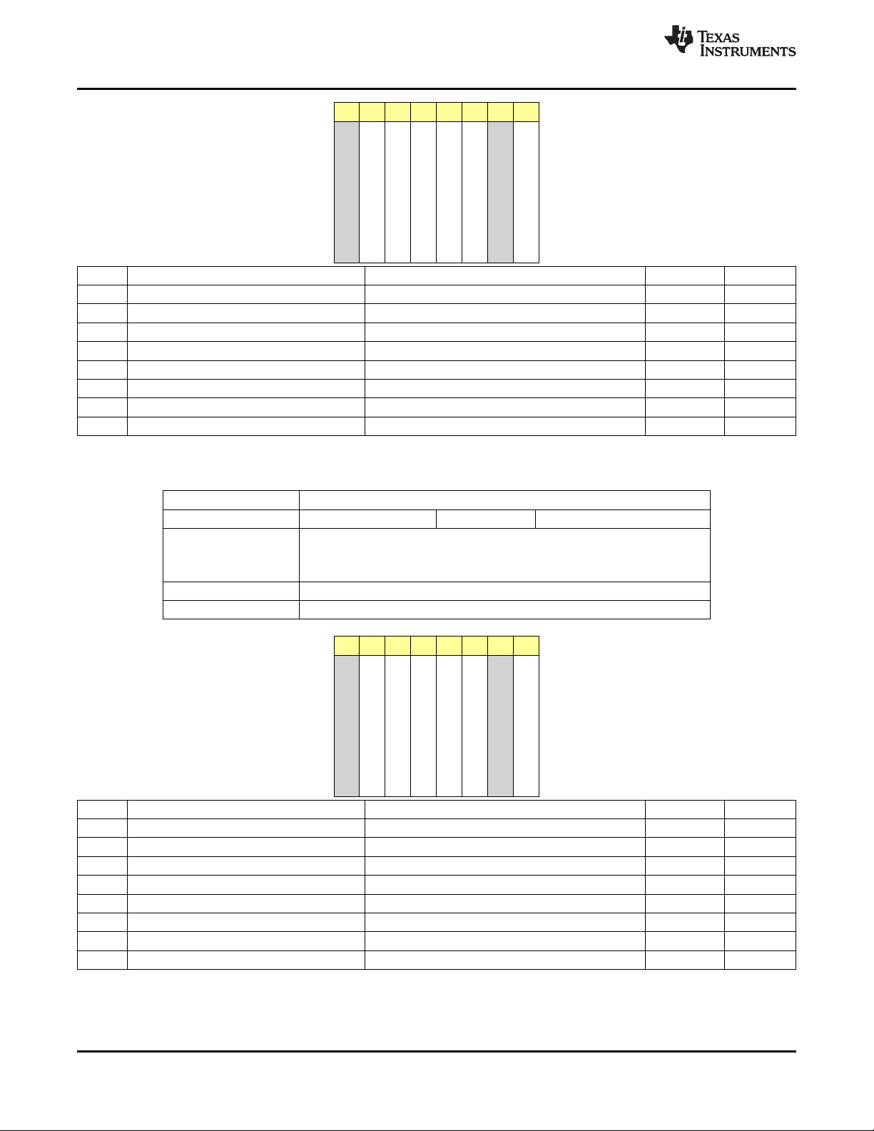
TUSB1210
SLLSE09D–NOVEMBER 2009–REVISED JANUARY 2011
7 6 5 4 3 2 1 0
SPARE
MNTR_VUSBIN_OK_EN
BITS FIELD NAME DESCRIPTION TYPE RESET
7 SPARE RW 0
6 MNTR_VUSBIN_OK_EN RW 0
5 ID_FLOAT_EN RW 0
4 ID_RES_EN RW 0
3 BVALID_FALL RW 0
2 BVALID_RISE RW 0
1 SPARE RW 0
0 ABNORMALSTRESS_EN RW 0
ID_RES_EN
ID_FLOAT_EN
BVALID_FALL
SPARE
BVALID_RISE
ABNORMALSTRESS_EN
www.ti.com
9.1.28 VENDOR_SPECIFIC1_CLR
ADDRESS OFFSET 0x3F
PHYSICAL ADDRESS 0x3F INSTANCE USB_SCUSB
DESCRIPTION This register doesn't physically exist.
It is the same as the func_ctrl register with read/clear-only property (write '1' to
clear a particular bit, a write '0' has no-action).
TYPE RW
WRITE LATENCY
7 6 5 4 3 2 1 0
SPARE
MNTR_VUSBIN_OK_EN
BITS FIELD NAME DESCRIPTION TYPE RESET
7 SPARE RW 0
6 MNTR_VUSBIN_OK_EN RW 0
5 ID_FLOAT_EN RW 0
4 ID_RES_EN RW 0
3 BVALID_FALL RW 0
2 BVALID_RISE RW 0
1 SPARE RW 0
0 ABNORMALSTRESS_EN RW 0
ID_RES_EN
ID_FLOAT_EN
BVALID_FALL
SPARE
BVALID_RISE
ABNORMALSTRESS_EN
46 Register Map Copyright © 2009–2011, Texas Instruments Incorporated
Submit Documentation Feedback
Product Folder Link(s): TUSB1210
Page 47
TUSB1210
www.ti.com
SLLSE09D–NOVEMBER 2009–REVISED JANUARY 2011
9.1.29 VENDOR_SPECIFIC2
ADDRESS OFFSET 0x80
PHYSICAL ADDRESS 0x80 INSTANCE USB_SCUSB
DESCRIPTION Eye diagram programmability and DP/DM swap control .
TYPE RW
WRITE LATENCY
7 6 5 4 3 2 1 0
IHSTX
SPARE
BITS FIELD NAME DESCRIPTION TYPE RESET
7 SPARE RW 0
6 DATAPOLARITY Control data polarity on dp/dm RW 1
5:04 ZHSDRV High speed output impedance configuration for eye diagram tuning : RW 0x0
00 45.455 Ω
01 43.779 Ω
10 42.793 Ω
11 42.411 Ω
3:00 IHSTX High speed output drive strength configuration for eye diagram tuning : RW 0x1
0000 17.928 mA
0001 18.117 mA
0010 18.306 mA
0011 18.495 mA
0100 18.683 mA
0101 18.872 mA
0110 19.061 mA
0111 19.249 mA
1000 19.438 mA
1001 19.627 mA
1010 19.816 mA
1011 20.004 mA
1100 20.193 mA
1101 20.382 mA
1110 20.570 mA
1111 20.759 mA
IHSTX[0] is also the AC BOOST enable
IHSTX[0] = 0 à AC BOOST is disabled
IHSTX[0] = 1 à AC BOOST is enabled
ZHSDRV
DATAPOLARITY
Copyright © 2009–2011, Texas Instruments Incorporated Register Map 47
Submit Documentation Feedback
Product Folder Link(s): TUSB1210
Page 48

TUSB1210
SLLSE09D–NOVEMBER 2009–REVISED JANUARY 2011
9.1.30 VENDOR_SPECIFIC2_SET
ADDRESS OFFSET 0x81
PHYSICAL ADDRESS 0x81 INSTANCE USB_SCUSB
DESCRIPTION This register doesn't physically exist.
It is the same as the VENDOR_SPECIFIC1 register with read/set-only property
(write '1' to set a particular bit, a write '0' has no-action).
TYPE RW
WRITE LATENCY
7 6 5 4 3 2 1 0
IHSTX
SPARE
BITS FIELD NAME DESCRIPTION TYPE RESET
7 SPARE RW 0
6 DATAPOLARITY RW 1
5:04 ZHSDRV RW 0x0
3:00 IHSTX RW 0x1
ZHSDRV
DATAPOLARITY
www.ti.com
9.1.31 VENDOR_SPECIFIC2_CLR
ADDRESS OFFSET 0x82
PHYSICAL ADDRESS 0x82 INSTANCE USB_SCUSB
DESCRIPTION This register doesn't physically exist.
It is the same as the VENDOR_SPECIFIC1 register with read/clear-only
property (write '1' to clear a particular bit, a write '0' has no-action).
TYPE RW
WRITE LATENCY
7 6 5 4 3 2 1 0
IHSTX
SPARE
BITS FIELD NAME DESCRIPTION TYPE RESET
7 SPARE RW 0
6 DATAPOLARITY RW 1
5:04 ZHSDRV RW 0x0
3:00 IHSTX RW 0x1
ZHSDRV
DATAPOLARITY
48 Register Map Copyright © 2009–2011, Texas Instruments Incorporated
Submit Documentation Feedback
Product Folder Link(s): TUSB1210
Page 49

TUSB1210
www.ti.com
SLLSE09D–NOVEMBER 2009–REVISED JANUARY 2011
9.1.32 VENDOR_SPECIFIC1_STS
ADDRESS OFFSET 0x83
PHYSICAL ADDRESS 0x83 INSTANCE USB_SCUSB
DESCRIPTION Indicates the current value of the interrupt source signal.
TYPE R
WRITE LATEN CY
7 6 5 4 3 2 1 0
Reserved
ID_RESB_STS
ID_RESC_STS
ID_FLOAT_STS
MNTR_VUSBIN_OK_STS
ABNORMALSTRESS_STS
BITS FIELD NAME DESCRIPTION TYPE RESET
7 Reserved R 0
6 MNTR_VUSBIN_OK_STS Current value of MNTR_VUSBIN_OK output R 0
5 ABNORMALSTRESS_STS Current value of ABNORMALSTRESS output R 0
4 ID_FLOAT_STS Current value of ID_FLOAT output R 0
3 ID_RESC_STS Current value of ID_RESC output R 0
2 ID_RESB_STS Current value of ID_RESB output R 0
1 ID_RESA_STS Current value of ID_RESA output R 0
0 BVALID_STS Current value of VB_SESS_VLD output R 0
BVALID_STS
ID_RESA_STS
9.1.33 VENDOR_SPECIFIC1_LATCH
ADDRESS OFFSET 0x84
PHYSICAL ADDRESS 0x84 INSTANCE USB_SCUSB
DESCRIPTION These bits are set by the PHY when an unmasked change occurs on the
corresponding internal signal. The PHY will automatically clear all bits when
the Link reads this register, or when Low Power Mode is entered. The PHY
also clears this register when Serial mode is entered regardless of the value of
ClockSuspendM.
The PHY follows the rules defined in Table 26 of the ULPI spec for setting any
latch register bit.
TYPE R
WRITE LATENCY
7 6 5 4 3 2 1 0
Reserved
ID_RESB_LATCH
ID_RESC_LATCH
ID_FLOAT_LATCH
MNTR_VUSBIN_OK_LATCH
ABNORMALSTRESS_LATCH
ID_RESA_LATCH
BVALID_LATCH
Copyright © 2009–2011, Texas Instruments Incorporated Register Map 49
Submit Documentation Feedback
Product Folder Link(s): TUSB1210
Page 50

TUSB1210
SLLSE09D–NOVEMBER 2009–REVISED JANUARY 2011
BITS FIELD NAME DESCRIPTION TYPE RESET
7 Reserved R 0
6 MNTR_VUSBIN_OK_LATCH Set to 1 when an unmasked event occurs on MNTR_VUSBIN_OK_LATCH. R 0
Clear on read register.
5 ABNORMALSTRESS_LATCH Set to 1 when an unmasked event occurs on ABNORMALSTRESS. Clear on R 0
read register.
4 ID_FLOAT_LATCH Set to 1 when an unmasked event occurs on ID_FLOAT. Clear on read R 0
register.
3 ID_RESC_LATCH Set to 1 when an unmasked event occurs on ID_RESC. Clear on read R 0
register.
2 ID_RESB_LATCH Set to 1 when an unmasked event occurs on ID_RESB. Clear on read R 0
register.
1 ID_RESA_LATCH Set to 1 when an unmasked event occurs on ID_RESA. Clear on read R 0
register.
0 BVALID_LATCH Set to 1 when an unmasked event occurs on VB_SESS_VLD. Clear on read R 0
register.
www.ti.com
9.1.34 VENDOR_SPECIFIC3
ADDRESS OFFSET 0x85
PHYSICAL ADDRESS 0x85 INSTANCE USB_SCUSB
DESCRIPTION
TYPE RW
WRITE LATENCY
7 6 5 4 3 2 1 0
SOF_EN
RESERVED
BITS FIELD NAME DESCRIPTION TYPE RESET
7 Reserved RW 0
6 SOF_EN 0: HS USB SOF detector disabled. RW 0
1: Enable HS USB SOF detection when PHY is set in device mode.
SOF are output on CPEN pin. HS USB SOF (start-of-frame) output
clock is available on CPEN pin when this bit is set. HS USB SOF
packet rate is 8 kHz.
This bit is provided for debugging purpose only. It must never been
write to ‘1’ in functional mode
5 CPEN_OD This bit has no effect when CPEN_ODOS = ‘0’, else : RW 0
0: CPEN pad is in OS (Open Source) mode.
In this case CPEN pin has an internal NMOS driver, and will be active
LOW.
Externally there should be a pullup resistor on CPEN (min 1kohm) to a
supply voltage (max 3.6V).
1: CPEN pad is in OD (Open Drain) mode
In this case CPEN pin has an internal PMOS driver, and will be active
HIGH.
Externally there should be a pull-down resistor on CPEN (min 1 kΩ to
GND.
CPEN_OD
CPEN_ODOS
IDGND_DRV
VUSB3V3_VSEL
50 Register Map Copyright © 2009–2011, Texas Instruments Incorporated
Submit Documentation Feedback
Product Folder Link(s): TUSB1210
Page 51

TUSB1210
www.ti.com
4 CPEN_ODOS Mode selection bit for CPEN pin. RW 0
0 : CPEN pad is in CMOS mode
1: CPEN pad is in OD (Open Drain) or OS (Open Source) mode
(controlled by CPEN_OD bit)
3 IDGND_DRV Drives ID pin to ground RW 0x0
2:00 VUSB3V3_VSEL 000 VRUSB3P1V = 2.5 V RW 0x3
001 VRUSB3P1V = 2.75 V
010 VRUSB3P1V = 3.0 V
011 VRUSB3P1V = 3.10 V (default)
100 VRUSB3P1V = 3.20 V
101 VRUSB3P1V = 3.30 V
110 VRUSB3P1V = 3.40 V
111 VRUSB3P1V = 3.50 V
SLLSE09D–NOVEMBER 2009–REVISED JANUARY 2011
9.1.35 VENDOR_SPECIFIC3_SET
ADDRESS OFFSET 0x86
PHYSICAL ADDRESS 0x86 INSTANCE USB_SCUSB
DESCRIPTION
TYPE RW
WRITE LATENCY
7 6 5 4 3 2 1 0
SOF_EN
RESERVED
BITS FIELD NAME DESCRIPTION TYPE RESET
7 Reserved RW 0
6 SOF_EN RW 0
5 CPEN_OD RW 0
4 CPEN _ODOS RW 0
3 IDGND_DRV RW 0x0
2:00 VUSB3V3_VSEL RW 0x3
CPEN_OD
CPEN_ODOS
IDGND_DRV
VUSB3V3_VSEL
9.1.36 VENDOR_SPECIFIC3_CLR
ADDRESS OFFSET 0x87
PHYSICAL ADDRESS 0x87 INSTANCE USB_SCUSB
DESCRIPTION
TYPE RW
WRITE LATENCY
7 6 5 4 3 2 1 0
SOF_EN
RESERVED
Copyright © 2009–2011, Texas Instruments Incorporated Register Map 51
Submit Documentation Feedback
Product Folder Link(s): TUSB1210
CPEN_OD
CPEN_ODOS
IDGND_DRV
VUSB3V3_VSEL
Page 52

TUSB1210
SLLSE09D–NOVEMBER 2009–REVISED JANUARY 2011
BITS FIELD NAME DESCRIPTION TYPE RESET
7 Reserved RW 0
6 SOF_EN RW 0
5 CPEN_OD RW 0
4 CPEN_ODOS RW 0
3 IDGND_DRV RW 0x0
2:00 VUSB3V3_VSEL RW 0x3
www.ti.com
52 Register Map Copyright © 2009–2011, Texas Instruments Incorporated
Submit Documentation Feedback
Product Folder Link(s): TUSB1210
Page 53

(See Note A)
(See Note C)
(See Note B)
(See Note D)
TUSB1210
Link Controller
V
DDIO
V
BUS
V
BUS
EN
IN
5 V
OUT
V
BAT
V
DD33
C
VDD18
C
VDDIO
C
BYP
C
VDD33
C
VDD15
C
VBUS
V
DD18
V
DD15
7
27
5
13
12
17
4
10
V
BUS
Switch
USB Receptacle
ESD
3
9
29
6
2
31
GND
GND
1.8-V Supply
V
DDIO
Supply
3.1 5.5 V–
Supply
V
DDIO
Supply
CPEN
CS_OUT
DIR
STP
RESETB
CLOCK
CLOCK
NXT
DATA0
DATA1
DATA2
DATA3
DATA4
DATA5
DATA6
DATA7
DIR
STP
RESETB
REFCLK
NXT
DATA0
DATA1
DATA2
DATA3
DATA4
DATA5
DATA6
DATA7
1
20
21
22
26
N/C
25
N/C
24
N/C
16
N/C
15
N/C
8
32
28, 30
14
11
CS
CFG
18
23
19
DP
DM
ID
DP
DM
ID
SHIELD
(See Note E)
TUSB1210
www.ti.com
10 Application Information
10.1 Host or OTG, ULPI Input Clock Mode Application
Figure 10-1 shows a suggested application diagram for TUSB1210 in the case of ULPI input-clock mode
(60 MHz ULPI clock is provided by link processor), in Host or OTG application. Note this is just one
example, it is of course possible to operate as HOST or OTG while also in ULPI output-clock mode.
SLLSE09D–NOVEMBER 2009–REVISED JANUARY 2011
10.2 Device, ULPI Output Clock Mode Application
Copyright © 2009–2011, Texas Instruments Incorporated Application Information 53
DDIO
A. Pin 11 (CS) : can be tied high to VIOif CS_OUT pin unavailable; Pin 14 (CFG) : tie-high is Don’t Care since ULPI
clock is used in input mode
B. Pin 1 (REFCLK) : must be tied low
C. Ext 3 V supply supported
D. Pin 27 (RESETB) can be tied to V
E. Pins labeled N/C (no-connect) are truly no-connect, and can be tied or left floating.
Figure 10-2 shows a suggested application diagram for TUSB1210 in the case of ULPI output clock mode
Figure 10-1. Host or OTG, ULPI Input Clock Mode Application Diagram
(60 MHz ULPI clock is provided by TUSB1210, while link processor or another external circuit provides
REFCLK), in Device mode application. Note this is just one example, it is of course possible to operate as
Device while also in ULPI input-clock mode. Refer also to Figure 10-1.
if unused.
Submit Documentation Feedback
Product Folder Link(s): TUSB1210
Page 54

(See Note A)
(See Note C)
(See Note B)
(See Note E)
(See Note D)
TUSB1210
Link Controller
V
DDIO
V
BUS
V
BUS
V
BAT
V
DD33
C
VDD18
C
VDDIO
C
BYP
C
VDD33
C
VDD15
C
VBUS
V
DD18
V
DD15
7
27
5
13
12
17
4
10
USB Receptacle
ESD
3
9
29
6
2
GND
GND
1.8-V Supply
V
DDIO
Supply
3.1 5.5 V–
Supply
V
DDIO
Supply
CPEN
CS_OUT
STP
RESETB
REFCLK
CLOCK
NXT
DATA0
DATA1
DATA2
DATA3
DATA4
DATA5
DATA6
DATA7
STP
RESETB
REFCLK
NXT
DATA0
DATA1
DATA2
DATA3
DATA4
DATA5
DATA6
DATA7
20
21
22
26
32
28, 30
31
DIR
DIR
1
CLKIN
14
11
CS
CFG
18
23
19
DP
DM
ID
DP
DM
SHIELD
N/C
25
N/C
24
N/C
16
N/C
15
N/C
8
TUSB1210
SLLSE09D–NOVEMBER 2009–REVISED JANUARY 2011
www.ti.com
54 Application Information Copyright © 2009–2011, Texas Instruments Incorporated
DDIO
A. Pin 11 (CS) : can be tied high to VIOif CS_OUT pin unavailable; Pin 14 (CFG) : Tied to V
mode here, tie to GND for 19.2MHz mode.
B. Pin 1 (REFCLK) : connect to external 3.3V square-wave reference clock
C. Ext 3 V supply supported
D. Pin 27 (RESETB) can be tied to V
E. Pins labeled N/C (no-connect) are truly no-connect, and can be tied or left floating.
Figure 10-2. Device, ULPI Output Clock Mode Application Diagram
if unused.
Submit Documentation Feedback
Product Folder Link(s): TUSB1210
for 26MHz REFCLK
DDIO
Page 55

TUSB1210
www.ti.com
11 Glossary
CMOS Complimentary Metal Oxide Semiconductor
DM Data manual
DSP Digital signal processor
ESD Electrostatic discharge
ESR Equivalent series resistance
hiZ High-impedance
HS High speed
HW Hardware
IC Integrated circuit
ID Identification
IDDQ Direct drain quiescent current
IF Interface
IO or I/O Input/output
JTAG Joint test action group, ieee 1149.1 standard
SLLSE09D–NOVEMBER 2009–REVISED JANUARY 2011
LDO Low dropout regulator
LS Low speed
NA Not applicable
OTG On the go
PBGA Plastic ball grid array
PCB Printed circuit board
PD Pulldown
PLL Phase locked loop
POL Polarity
PSRR Power supply rejection ratio
PU Pullup
RX Receive
SW Software
Copyright © 2009–2011, Texas Instruments Incorporated Glossary 55
Submit Documentation Feedback
Product Folder Link(s): TUSB1210
Page 56

TUSB1210
SLLSE09D–NOVEMBER 2009–REVISED JANUARY 2011
SYNC/SYNCHRO Synchronization
SYS System
TBD To be defined
TRM Technical reference manual
TX Transmit
UART Universal asynchronous receiver transmitter
ULPI UTMI+ low pin interface
USB Universal serial bus
UTMI USB transceiver macrocell interface
www.ti.com
56 Glossary Copyright © 2009–2011, Texas Instruments Incorporated
Submit Documentation Feedback
Product Folder Link(s): TUSB1210
Page 57

Pin 1 Indicator
TUSB1210RHB
YMLLLLS
$
TUSB1210
www.ti.com
12 TUSB1210 Package
12.1 TUSB1210 Standard Package Symbolization
Figure 12-1. Printed Device Reference
Table 12-1. TUSB1210 Nomenclature Description
FIELDS MEANING
P Marking used to note prototype (X), preproduction (P), or
qualified/production device (Blank)(1)
A Mask set version descriptor (initial silicon = BLANK, first
silicon revision = A, second silicon revision = B,...)(2)
YM Year month
LLLLS Lot code
$ Fab Planning Code
SLLSE09D–NOVEMBER 2009–REVISED JANUARY 2011
12.2 Package Thermal Resistance Characteristics
Table 12-2 provides the thermal resistance characteristics for the recommended package type RHB
(S-PQFP-N32) used for the TUSB1210 device. Refer to the application report IC Package Thermal
Metrics, TI literature number SPRA953, further details concerning parameter definitions and usage.
Table 12-2. TUSB1210 Thermal Resistance Characteristics
PARAMETER VALUE UNIT MEASUREMENT METHOD
q
JA
q
JC
q
JC
bottom
q
JB
Ψ
JT
Ψ
JB
(1) Top is surface of the package facing away from the PCB.
(2) Refer to measurement method in Chapter 2 of IC Package Thermal Metrics, TI literature number SPRA953.
(3) Bottom surface is the surface of the package facing towards the PCB.
Copyright © 2009–2011, Texas Instruments Incorporated TUSB1210 Package 57
Junction-to-ambient thermal resistance 34.72 °C/W EIA/JESD 51-1
top Junction-to-case top thermal resistance
Junction-to-case bottom thermal resistance
Junction-to-board thermal resistance or 10.3 °C/W EIA/ JESD 51-8.
junction-to-pin thermal resistance
Junction-to-top of package (not a true thermal 0.5 °C/W EIA/JESD 51-2
resistance)
Junction-to-board (not a true thermal resistance) 10.5 °C/W EIA/JESD 51-6
(1)
(3)
Submit Documentation Feedback
Product Folder Link(s): TUSB1210
37.3 °C/W No current JEDEC specification
3.6 °C/W No current JEDEC specification
(2)
(2)
Page 58

PACKAGE OPTION ADDENDUM
www.ti.com
12-Jan-2011
PACKAGING INFORMATION
Orderable Device
TUSB1210BRHB PREVIEW QFN RHB 32 1 TBD Call TI Call TI Samples Not Available
TUSB1210BRHBR PREVIEW QFN RHB 32 1 TBD Call TI Call TI Samples Not Available
(1)
The marketing status values are defined as follows:
ACTIVE: Product device recommended for new designs.
LIFEBUY: TI has announced that the device will be discontinued, and a lifetime-buy period is in effect.
NRND: Not recommended for new designs. Device is in production to support existing customers, but TI does not recommend using this part in a new design.
PREVIEW: Device has been announced but is not in production. Samples may or may not be available.
OBSOLETE: TI has discontinued the production of the device.
Status
(1)
Package Type Package
Drawing
Pins Package Qty
Eco Plan
(2)
Lead/
Ball Finish
MSL Peak Temp
(3)
Samples
(Requires Login)
(2)
Eco Plan - The planned eco-friendly classification: Pb-Free (RoHS), Pb-Free (RoHS Exempt), or Green (RoHS & no Sb/Br) - please check http://www.ti.com/productcontent for the latest availability
information and additional product content details.
TBD: The Pb-Free/Green conversion plan has not been defined.
Pb-Free (RoHS): TI's terms "Lead-Free" or "Pb-Free" mean semiconductor products that are compatible with the current RoHS requirements for all 6 substances, including the requirement that
lead not exceed 0.1% by weight in homogeneous materials. Where designed to be soldered at high temperatures, TI Pb-Free products are suitable for use in specified lead-free processes.
Pb-Free (RoHS Exempt): This component has a RoHS exemption for either 1) lead-based flip-chip solder bumps used between the die and package, or 2) lead-based die adhesive used between
the die and leadframe. The component is otherwise considered Pb-Free (RoHS compatible) as defined above.
Green (RoHS & no Sb/Br): TI defines "Green" to mean Pb-Free (RoHS compatible), and free of Bromine (Br) and Antimony (Sb) based flame retardants (Br or Sb do not exceed 0.1% by weight
in homogeneous material)
(3)
MSL, Peak Temp. -- The Moisture Sensitivity Level rating according to the JEDEC industry standard classifications, and peak solder temperature.
Important Information and Disclaimer:The information provided on this page represents TI's knowledge and belief as of the date that it is provided. TI bases its knowledge and belief on information
provided by third parties, and makes no representation or warranty as to the accuracy of such information. Efforts are underway to better integrate information from third parties. TI has taken and
continues to take reasonable steps to provide representative and accurate information but may not have conducted destructive testing or chemical analysis on incoming materials and chemicals.
TI and TI suppliers consider certain information to be proprietary, and thus CAS numbers and other limited information may not be available for release.
In no event shall TI's liability arising out of such information exceed the total purchase price of the TI part(s) at issue in this document sold by TI to Customer on an annual basis.
Addendum-Page 1
Page 59
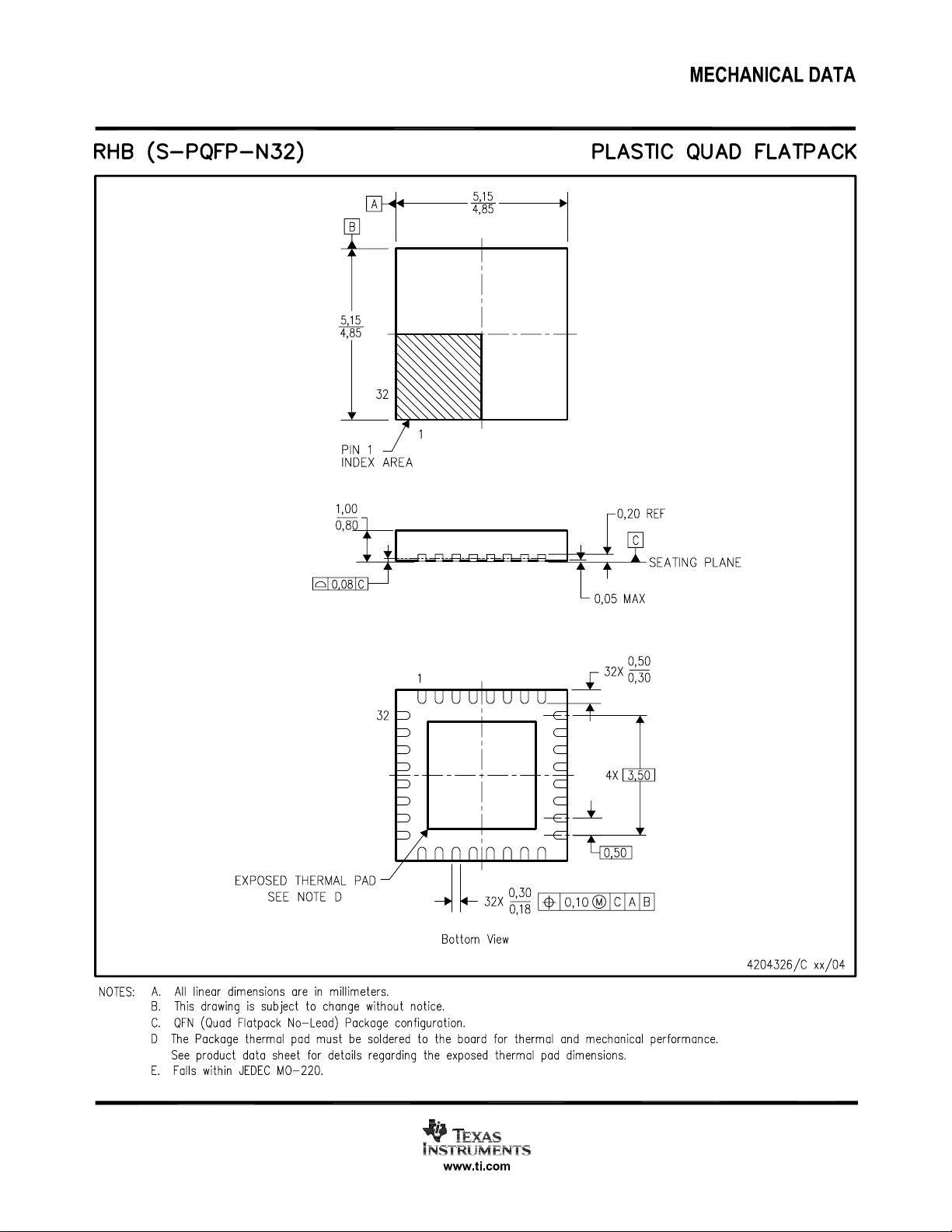
Page 60

IMPORTANT NOTICE
Texas Instruments Incorporated and its subsidiaries (TI) reserve the right to make corrections, modifications, enhancements, improvements,
and other changes to its products and services at any time and to discontinue any product or service without notice. Customers should
obtain the latest relevant information before placing orders and should verify that such information is current and complete. All products are
sold subject to TI’s terms and conditions of sale supplied at the time of order acknowledgment.
TI warrants performance of its hardware products to the specifications applicable at the time of sale in accordance with TI’s standard
warranty. Testing and other quality control techniques are used to the extent TI deems necessary to support this warranty. Except where
mandated by government requirements, testing of all parameters of each product is not necessarily performed.
TI assumes no liability for applications assistance or customer product design. Customers are responsible for their products and
applications using TI components. To minimize the risks associated with customer products and applications, customers should provide
adequate design and operating safeguards.
TI does not warrant or represent that any license, either express or implied, is granted under any TI patent right, copyright, mask work right,
or other TI intellectual property right relating to any combination, machine, or process in which TI products or services are used. Information
published by TI regarding third-party products or services does not constitute a license from TI to use such products or services or a
warranty or endorsement thereof. Use of such information may require a license from a third party under the patents or other intellectual
property of the third party, or a license from TI under the patents or other intellectual property of TI.
Reproduction of TI information in TI data books or data sheets is permissible only if reproduction is without alteration and is accompanied
by all associated warranties, conditions, limitations, and notices. Reproduction of this information with alteration is an unfair and deceptive
business practice. TI is not responsible or liable for such altered documentation. Information of third parties may be subject to additional
restrictions.
Resale of TI products or services with statements different from or beyond the parameters stated by TI for that product or service voids all
express and any implied warranties for the associated TI product or service and is an unfair and deceptive business practice. TI is not
responsible or liable for any such statements.
TI products are not authorized for use in safety-critical applications (such as life support) where a failure of the TI product would reasonably
be expected to cause severe personal injury or death, unless officers of the parties have executed an agreement specifically governing
such use. Buyers represent that they have all necessary expertise in the safety and regulatory ramifications of their applications, and
acknowledge and agree that they are solely responsible for all legal, regulatory and safety-related requirements concerning their products
and any use of TI products in such safety-critical applications, notwithstanding any applications-related information or support that may be
provided by TI. Further, Buyers must fully indemnify TI and its representatives against any damages arising out of the use of TI products in
such safety-critical applications.
TI products are neither designed nor intended for use in military/aerospace applications or environments unless the TI products are
specifically designated by TI as military-grade or "enhanced plastic." Only products designated by TI as military-grade meet military
specifications. Buyers acknowledge and agree that any such use of TI products which TI has not designated as military-grade is solely at
the Buyer's risk, and that they are solely responsible for compliance with all legal and regulatory requirements in connection with such use.
TI products are neither designed nor intended for use in automotive applications or environments unless the specific TI products are
designated by TI as compliant with ISO/TS 16949 requirements. Buyers acknowledge and agree that, if they use any non-designated
products in automotive applications, TI will not be responsible for any failure to meet such requirements.
Following are URLs where you can obtain information on other Texas Instruments products and application solutions:
Products Applications
Audio www.ti.com/audio Communications and Telecom www.ti.com/communications
Amplifiers amplifier.ti.com Computers and Peripherals www.ti.com/computers
Data Converters dataconverter.ti.com Consumer Electronics www.ti.com/consumer-apps
DLP® Products www.dlp.com Energy and Lighting www.ti.com/energy
DSP dsp.ti.com Industrial www.ti.com/industrial
Clocks and Timers www.ti.com/clocks Medical www.ti.com/medical
Interface interface.ti.com Security www.ti.com/security
Logic logic.ti.com Space, Avionics and Defense www.ti.com/space-avionics-defense
Power Mgmt power.ti.com Transportation and www.ti.com/automotive
Microcontrollers microcontroller.ti.com Video and Imaging www.ti.com/video
RFID www.ti-rfid.com Wireless www.ti.com/wireless-apps
RF/IF and ZigBee® Solutions www.ti.com/lprf
TI E2E Community Home Page e2e.ti.com
Automotive
Mailing Address: Texas Instruments, Post Office Box 655303, Dallas, Texas 75265
Copyright © 2011, Texas Instruments Incorporated
 Loading...