

Page 1
PC
USB
CLK
AC-to-DC
5V PS
AC-to-DC
19V PS
TSW4806
(Clock Gen)
TSW2110
ADS4249
(Dual ADC)
TSW1400
(Data Capt)
TSW2200
(Pwr dist)
User's Guide
SLAU438–March 2012
TSW2110EVM Evaluation Module (EVM)
This user’s guide describes the operation of the TSW2110 input signal generator evaluation module
(EVM). The 10-MHz EVM is used to verify the functionality of various TI analog-to-digital converters
(ADCs). The guide includes setup instructions for the hardware, expected results captured from a
TSW1400EVM and an ADS4249EVM. The TSW2110EVM product folder on the TI web site contains the
EVM schematic, bill of materials, and layout files.
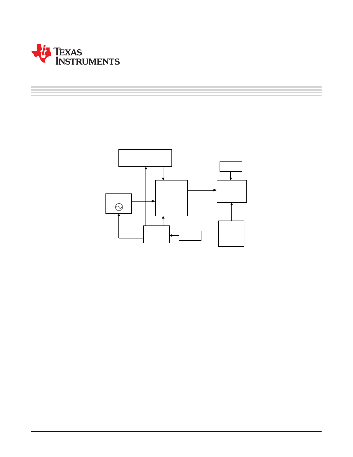
1 Introduction
The TI TSW2110EVM (EVM) helps designers evaluate the functionality of their ADC devices. This product
eliminates the expense of using a signal generator to create an input signal.
The board is powered off a bench power supply or the 5-V output which is found on the TSW2200EVM. A
red and black banana jack to easy hook patch cable delivers the required voltage to the EVM. An external
clock generator is required to provide a sampling clock for the ADC board to capture correctly. For the
captures conducted in this document, a 245.76-MHz clocking signal from the TSW4806EVM was used.
The EVM has a default setup expecting an input voltage of 5 V. With this voltage applied, a temperaturecontrolled crystal oscillator (TCXO) generates a HCMOS waveform at 10 MHz. Using amplification,
attenuation and filtering, a 10-MHz signal is generated with low harmonic distortion output. The output
waveform is set to +10 dBm (2 Vpp), which is used as the input to an ADC board.
The TCXO is powered from the 3.3-V output of the low-dropout (LDO) regulator in its default mode. This
applied voltage generates a 10-MHz, HCMOS signal with an amplitude of 10.6 dBm.
The output waveform of the TCXO is attenuated by a 15dB pad prior to going into the input of the
amplifier. This amplifier requires an input signal with an amplitude of approximately –5 dBm. At this input
level, a gain of 20 dB is achieved without creating additional harmonic distortion. The amplifier output
waveform is +15 dBm and has significant harmonics. A crystal filter (part number, FTR-80307) is
necessary to eliminate these harmonics. A 1db pad is installed after the amplifier to maintain 50-Ω
termination and reduce the impact of impedance mismatches.
Figure 1. Block Diagram for Testing
SLAU438–March 2012 TSW2110EVM Evaluation Module (EVM)
Submit Documentation Feedback
Copyright © 2012, Texas Instruments Incorporated
1
Page 2
Evaluation with the TSW2110
On the 8-pole crystal filter, FTR-80307, matching is tuned for optimal performance. This matching is
crucial for proper filter behavior and does not result in low output power. This filter attenuates the
harmonics lower than –80 dBc resulting in a clean sine wave that is used as an input to the ADC board.
Depending on which ADC is evaluated, the resulting carrier amplitude should be approximately –1 dBFS.
For information on the filter, contact PDI at www.pdixtal.com.
2 Evaluation with the TSW2110
This chapter details the evaluation process and features of the EVM. An external supply voltage must be
connected to the voltage in and ground test points (TP1 and TP2, respectively). A blue LED turns on if the
proper voltage is supplied. An SMA to SMA cable must be connected from the output SMA connector to
the input channel of the unit under test.
The board accepts a supply voltage of 5 V (default) or 3.3 V. Different jumper configurations are
necessary for these two options. If the board is supplied with 5 V, the charge pump is bypassed and the
LDO 3.3-V regulator is implemented. If 3.3 V is supplied, the regulator is bypassed and the charge pump
is used. The necessary configurations for each method are seen in Table 1. The board is clearly marked
with these points so that the proper jumper configuration can be implemented. Improper jumpers will not
damage the parts on the board; however, the system will not create the desired waveform for accurate
testing.
Option JP1 JP2, JP3 JP4, JP5
5 V (default) Short 1-2 Opened Shorted
3.3 V Short 2-3 Shorted Opened
www.ti.com
Table 1. Jumper Configurations
3 Measurements
When the board is functioning properly, the output waveform measured on the SMA connector should
have 10 dBm of amplitude. The best way to get an accurate reading is when measured on a signal
analyzer with a 50-Ω load termination. The testing for this user’s guide was done on a spectrum analyzer.
On many signal analyzers, the EVM output signal overdrives the machine in their default settings. RF
attenuation must be set to account for this. The data taken in Figure 2 had the RF attenuation set to 25 dB
and set to 5 dB in Figure 3.
2
TSW2110EVM Evaluation Module (EVM) SLAU438–March 2012
Copyright © 2012, Texas Instruments Incorporated
Submit Documentation Feedback
Page 3

www.ti.com
Measurements
Figure 2. Output Waveform At 10 MHz, Signal At 10.1 dBm
The output is filtered with a 10-MHz rejection filter to keep from distorting the analyzer. Figure 3 shows the
performance of the EVM at the second through fifth harmonics. The highest is the second harmonic at
74.2 dBm.
Figure 3. Waveform Harmonics At 91.4, 74.2, 99.82, and 103.59 dBm
SLAU438–March 2012 TSW2110EVM Evaluation Module (EVM)
Submit Documentation Feedback
Copyright © 2012, Texas Instruments Incorporated
3
Page 4

Measurements
3.1 Expected Values
Table 2 and Table 3 outline the expected values for certain test points on the board to monitor the
functionality of the TSW2110. Depending on the input voltage configuration on the board, some of the
expected values are different. The charge pump draws more current in the 3.3-V input configuration than
the LDO regulator does with the 5-V input.
3.2 Output Waveform
www.ti.com
Table 2. Expected Values With a 5-V Input
System Current 115 mA
Input Voltage 5 V
Amplifier Voltage 4.98 V
Table 3. Expected Values With a 3.3-V Input
System Current 190 mA
Input Voltage 3.3 V
Amplifier Voltage 5.01 V
Figure 4. Capture on TSW1400 of the ADS4249EVM, Input Signal Source Is TSW2110
The data captured meets datasheet-type performance for the ADS4249EVM.
4
TSW2110EVM Evaluation Module (EVM) SLAU438–March 2012
Copyright © 2012, Texas Instruments Incorporated
Submit Documentation Feedback
Page 5

www.ti.com
Measurements
Figure 5. TSW2110EVM Board
SLAU438–March 2012 TSW2110EVM Evaluation Module (EVM)
Submit Documentation Feedback
Copyright © 2012, Texas Instruments Incorporated
5
Page 6

IMPORTANT NOTICE
Texas Instruments Incorporated and its subsidiaries (TI) reserve the right to make corrections, modifications, enhancements, improvements,
and other changes to its products and services at any time and to discontinue any product or service without notice. Customers should
obtain the latest relevant information before placing orders and should verify that such information is current and complete. All products are
sold subject to TI’s terms and conditions of sale supplied at the time of order acknowledgment.
TI warrants performance of its hardware products to the specifications applicable at the time of sale in accordance with TI’s standard
warranty. Testing and other quality control techniques are used to the extent TI deems necessary to support this warranty. Except where
mandated by government requirements, testing of all parameters of each product is not necessarily performed.
TI assumes no liability for applications assistance or customer product design. Customers are responsible for their products and
applications using TI components. To minimize the risks associated with customer products and applications, customers should provide
adequate design and operating safeguards.
TI does not warrant or represent that any license, either express or implied, is granted under any TI patent right, copyright, mask work right,
or other TI intellectual property right relating to any combination, machine, or process in which TI products or services are used. Information
published by TI regarding third-party products or services does not constitute a license from TI to use such products or services or a
warranty or endorsement thereof. Use of such information may require a license from a third party under the patents or other intellectual
property of the third party, or a license from TI under the patents or other intellectual property of TI.
Reproduction of TI information in TI data books or data sheets is permissible only if reproduction is without alteration and is accompanied
by all associated warranties, conditions, limitations, and notices. Reproduction of this information with alteration is an unfair and deceptive
business practice. TI is not responsible or liable for such altered documentation. Information of third parties may be subject to additional
restrictions.
Resale of TI products or services with statements different from or beyond the parameters stated by TI for that product or service voids all
express and any implied warranties for the associated TI product or service and is an unfair and deceptive business practice. TI is not
responsible or liable for any such statements.
TI products are not authorized for use in safety-critical applications (such as life support) where a failure of the TI product would reasonably
be expected to cause severe personal injury or death, unless officers of the parties have executed an agreement specifically governing
such use. Buyers represent that they have all necessary expertise in the safety and regulatory ramifications of their applications, and
acknowledge and agree that they are solely responsible for all legal, regulatory and safety-related requirements concerning their products
and any use of TI products in such safety-critical applications, notwithstanding any applications-related information or support that may be
provided by TI. Further, Buyers must fully indemnify TI and its representatives against any damages arising out of the use of TI products in
such safety-critical applications.
TI products are neither designed nor intended for use in military/aerospace applications or environments unless the TI products are
specifically designated by TI as military-grade or "enhanced plastic." Only products designated by TI as military-grade meet military
specifications. Buyers acknowledge and agree that any such use of TI products which TI has not designated as military-grade is solely at
the Buyer's risk, and that they are solely responsible for compliance with all legal and regulatory requirements in connection with such use.
TI products are neither designed nor intended for use in automotive applications or environments unless the specific TI products are
designated by TI as compliant with ISO/TS 16949 requirements. Buyers acknowledge and agree that, if they use any non-designated
products in automotive applications, TI will not be responsible for any failure to meet such requirements.
Following are URLs where you can obtain information on other Texas Instruments products and application solutions:
Products Applications
Audio www.ti.com/audio Automotive and Transportation www.ti.com/automotive
Amplifiers amplifier.ti.com Communications and Telecom www.ti.com/communications
Data Converters dataconverter.ti.com Computers and Peripherals www.ti.com/computers
DLP® Products www.dlp.com Consumer Electronics www.ti.com/consumer-apps
DSP dsp.ti.com Energy and Lighting www.ti.com/energy
Clocks and Timers www.ti.com/clocks Industrial www.ti.com/industrial
Interface interface.ti.com Medical www.ti.com/medical
Logic logic.ti.com Security www.ti.com/security
Power Mgmt power.ti.com Space, Avionics and Defense www.ti.com/space-avionics-defense
Microcontrollers microcontroller.ti.com Video and Imaging www.ti.com/video
RFID www.ti-rfid.com
OMAP Mobile Processors www.ti.com/omap
Wireless Connectivity www.ti.com/wirelessconnectivity
TI E2E Community Home Page e2e.ti.com
Mailing Address: Texas Instruments, Post Office Box 655303, Dallas, Texas 75265
Copyright © 2012, Texas Instruments Incorporated
 Loading...