

Page 1

User's Guide
SLWU079– February 2012
TSW140x High Speed Data Capture/Pattern Generator
Card
The Texas Instruments TSW1400 Evaluation Module (EVM) is a next generation of pattern generator and
data capture card used to evaluate performances of a wide range of Texas Instruments (TI) high-speed
analog-to-digital converters (ADC) and digital-to-analog converters (DAC). For an ADC, capturing the
sampled data over an LVDS interface when using a high-quality, low-jitter clock, and a high-quality input
frequency, the TSW1400 can be used to demonstrate data sheet performance specifications. Together
with the accompanying Labview based Graphic User Interface (GUI), it is a complete system that captures
and evaluates data samples from ADC EVM’s and generates and sends desired test patterns to DAC
EVM’s
The TSW1405 is a low cost data capture card with limited capabilities as compared with the TSW1400.
The TSW1405 supports pattern capture for most LVDS format TI ADC EVMs, but with a capture buffer
limitation of 64K samples. The TSW1405 draws its power from the USB connection to the PC for easy
setup and operation. The same TSW1400 Graphical User Interface supports the TSW1405 as well,
making for a consistent feel across the different platforms.
The TSW1406 is a low cost pattern generator card with limited capabilities as compared with the
TSW1400. The TSW1406 supports pattern generation for most LVDS format TI DAC EVMs, but with a
pattern limitation of 64K samples. The TSW1406 draws its power from the USB connection to the PC for
easy setup and operation. The same TSW1400 GUI supports the TSW1406 as well.
Table 1. TSW140x EVM Features
I/O Interface
LVDS CMOS JESD 16 Bit Memory Depth Data Capture Data Source
TSW1400 Yes Firmware Firmware 512M Yes Yes
TSW1405 Yes No No 64K Yes No
TSW1406 Yes No No 64K No Yes
1 Functionality ................................................................................................................. 3
1.1 ADC EVM Data Capture .......................................................................................... 4
1.2 DAC EVM Pattern Generator ..................................................................................... 4
2 Hardware Configuration .................................................................................................... 4
2.1 Power Connections ................................................................................................ 5
2.2 Switches, Jumpers and Fuses ................................................................................... 5
2.3 LED's ................................................................................................................ 6
2.4 Connectors .......................................................................................................... 6
3 Software Start up ........................................................................................................... 7
3.1 Installation Instructions ............................................................................................ 7
3.2 USB Interface and Drivers ........................................................................................ 8
3.3 Device ini Files .................................................................................................... 10
4 User Interface .............................................................................................................. 10
4.1 Toolbar ............................................................................................................. 11
4.2 Status Windows ................................................................................................... 14
All trademarks are the property of their respective owners.
Future Future
Release Release
Contents
SLWU079– February 2012 TSW140x High Speed Data Capture/Pattern Generator Card
Submit Documentation Feedback
Copyright © 2012, Texas Instruments Incorporated
1
Page 2

www.ti.com
4.3 Mode Selection ................................................................................................... 15
4.4 Device Selection .................................................................................................. 15
4.5 Capture Button (ADC Mode only) .............................................................................. 16
4.6 Test Selection (ADC Mode only) ............................................................................... 16
4.7 DAC Display Panel (DAC Mode only) ......................................................................... 21
4.8 I/Q Multi-tone Generator ......................................................................................... 23
5 ADC Data Capture Software Operation ................................................................................ 23
5.1 Testing with an ADS5281 EVM ................................................................................. 23
6 TSW1400 Pattern Generator Operation ................................................................................ 27
6.1 Testing with DAC3152 EVM .................................................................................... 27
6.2 Loading DAC Firmware .......................................................................................... 27
6.3 Configuring TSW1400 for Pattern Generation ................................................................ 29
List of Figures
1 TSW1400EVM Block Diagram ............................................................................................ 3
2 TSW1400EVM Serial Number............................................................................................. 8
3 Firmware Does Not Match the Device Selected........................................................................ 8
4 TSW1400EVM GUI Top Level ............................................................................................ 9
5 Connecting GUI to EVM ................................................................................................... 9
6 Hardware Device Manager............................................................................................... 10
7 File Tab Options........................................................................................................... 11
8 Instrument Options ........................................................................................................ 11
9 Capture Option............................................................................................................. 12
10 Test Options................................................................................................................ 12
11 Notch Frequency Bin removal .......................................................................................... 13
12 Two Channel Display ..................................................................................................... 14
13 Status Window............................................................................................................. 15
14 Center Status Window.................................................................................................... 15
15 TSW1400 Modes.......................................................................................................... 15
16 ADC Device Selection Window.......................................................................................... 16
17 Single Tone FFT Display................................................................................................. 17
18 Data Display Options ..................................................................................................... 18
19 Channel Selection Window............................................................................................... 18
20 Data Windowing Options ................................................................................................. 18
21 ADC 2nd Input Frequency Box .......................................................................................... 20
22 DAC Display Mode........................................................................................................ 21
23 DAC Test Pattern Display................................................................................................ 22
24 TSW1400EVM interfacing to an ADS5281 EVM...................................................................... 24
25 ADC5281 Single Tone FFT Capture Results.......................................................................... 25
26 Devices Supported with Current Firmware Load...................................................................... 26
27 TSW1400 EVM Interfacing to a DAC EVM ............................................................................ 27
28 TSW1400EVM GUI DAC Mode Top Level............................................................................. 28
29 DAC Selection ............................................................................................................. 28
30 TSW1400 Output Data to DAC EVM ................................................................................... 29
2
TSW140x High Speed Data Capture/Pattern Generator Card SLWU079– February 2012
Copyright © 2012, Texas Instruments Incorporated
Submit Documentation Feedback
Page 3
ADC
EVM
DAC LVDS INTERFACE
1GB DDR RAM
ALTERA
STRATIX IV
(FIRMWARE)
USB
to
SERIAL
SPI
Interface
USB
PORT
Data and Clock
Signals
TSW1400 EVM
DAC
EVM
Pattern and
Data Clock
ADC / DAC CMOS
INTERFACE
ADC LVDS INTERFACE
www.ti.com
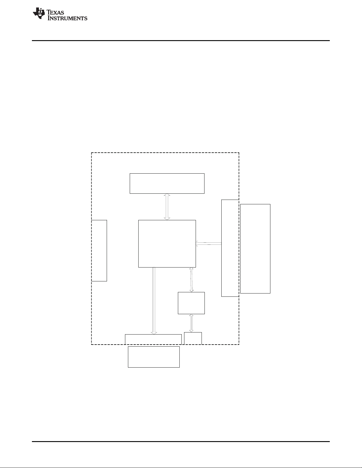
1 Functionality
The TSW1400 has two direct interfaces to TI ADC EVM’s. One option captures data through a LVDS
interface and the other uses a CMOS interface (currently not supported). Sampled data from the ADC is
de-serialized and formatted by an Altera Stratix IV FPGA, then stored into an external onboard 1GB DDR
memory card. The onboard memory enables the TSW1400 to store up to 512M 16 bit data samples. To
acquire data on a host PC, the FPGA reads the data from memory and transmits it on Serial Peripheral
Interface (SPI). An onboard high speed USB to SPI converter bridges the FPGA SPI interface to the host
PC and GUI.
The TSW1400 has two direct interfaces to TI DAC EVM’s. In Pattern Generator Mode, the TSW1400
generates desired test patterns for DAC EVM’s under test. These patterns are sent from the host PC over
the USB interface to the TSW1400. The FPGA stores the data received into the board DDR memory
module. The data from the memory is then read by the FPGA and transmitted to a DAC EVM either
across a DAC LVDS interface connector or a CMOS interface connector (currently not supported).
A block diagram of the TSW1400 EVM is shown in Figure 1.
Functionality
Figure 1. TSW1400EVM Block Diagram
SLWU079– February 2012 TSW140x High Speed Data Capture/Pattern Generator Card
Submit Documentation Feedback
Copyright © 2012, Texas Instruments Incorporated
3
Page 4

Hardware Configuration
1.1 ADC EVM Data Capture
Many TI high-speed ADCs have LVDS outputs for the digitized data. These ADCs are generally available
on an EVM that connects directly to the TSW1400EVM. The common connector between the ADC EVM
and the TSW1400EVM is a Samtec high-speed connector with differential pairs routed to adjacent pins
and the pairs separated by a ground pin. A common pinout for the connector across a family of EVMs has
been established. At present, the interface between the ADC EVM and the TSW1400EVM has defined
connections for 35 pairs of LVDS data lines, two clock pairs, and eight general purpose CMOS I/O pins.
The TSW1400 has a CMOS interface that is currently unsupported in this release.
The data format for the LVDS data bus can be in one of many formats, all supported by the TSW1400.
For single-channel, high-speed ADCs, the data format is commonly a parallel dual-data rate with one
output clock . Dual-data rate means that both the rising and falling edges of the clock register data into the
TSW1400. For multichannel ADCs, the data is commonly presented in a serialized format, where
individual bits of the output data are presented on an LVDS pair one bit at a time, at a higher data rate
than the sample rate of the ADC.
Several firmware files are used by the FPGA on the TSW1400 to accommodate both parallel DDR formats
an serial LVDS formats, although not at the same time. The GUI will load the FPGA with the appropriate
firmware based on the ADC EVM under test selected by the user.
The parallel DDR FPGA program supports several types of data formats. One common format presents
odd-numbered data bits on the bus on one clock edge and even-numbered data bits on the bus on the
other clock edge. This format is commonly used for ADCs with sampling rates up to 250 MHz. For this
bit-wise DDR format, the parallel data bus uses half as many LVDS pairs as there are bits in the sample.
For example, a 16-bit ADC uses eight LVDS pairs for data plus an LVDS clock pair for bit-wise DDR. For
higher sample rates up to 1 GHz, a sample-wise DDR format is often used. For sample-wise DDR, the
data bus width has as many LVDS pairs as the bit resolution of the ADC. On one clock edge, a data
sample from the ADC is registered; on the next clock edge, the next data sample from the ADC is
registered.
The serial FPGA program also supports several data formats. For one-wire serial formats, the data is
serialized onto a single LVDS pair at a rate that is 12 times the sample rate for an ADC with a 12-bit
resolution. A one-wire serialization format also is used for 14-bit and 16-bit data at data rates 14 or 16
times the sample rate, respectively. For serial data formats, a DDR LVDS bit clock is used to strobe the
serial data bits and to de-serialize the data. An additional clock pair operating at the sample rate of the
ADC identifies the sample-word boundaries in the serial data. For multichannel ADCs, a single-bit clock
and a single sample-rate clock (frame clock) is used for all of the LVDS data channels. The other common
serial data format is two-wire serialization. Two-wire serialization is similar to one-wire serialization except
that a data channel uses two LVDS pairs to carry the serialized data at a rate that is half of what it is for
one-wire serialization.
www.ti.com
1.2 DAC EVM Pattern Generator
Some TI high-speed DAC’s have LVDS inputs for the digitized data. These DACs are generally available
on an EVM that connects directly to the TSW1400EVM. The common connector between the DAC EVM
and the TSW1400EVM is a Samtec high-speed connector with differential pairs routed to adjacent pins
and the pairs separated by a ground pin. A common pinout for the connector across a family of EVMs has
been established. At present, the interface between these DAC EVM’s and the TSW1400EVM has defined
connections for 32 pairs of LVDS data lines, two data output clock pairs, four control pairs, two input clock
pairs (sync, strobes, and so on), eight general purpose CMOS I/O pins (USB controlled) and 10 general
purpose CMOS I/O pins (FPGA controlled). The TSW1400 has a CMOS interface that is currently
unsupported. If the DAC EVM supports a CMOS single-ended format, then the TSW3100 system is
intended to be used.
2 Hardware Configuration
In this section, the various portions of the TSW1400EVM hardware are described.
4
TSW140x High Speed Data Capture/Pattern Generator Card SLWU079– February 2012
Copyright © 2012, Texas Instruments Incorporated
Submit Documentation Feedback
Page 5

www.ti.com
2.1 Power Connections
The TSW1400EVM hardware is designed to operate from a single-supply voltage of 5 Vdc. The power
input is controlled by the ON/OFF switch SW7. Make sure this switch is in the “OFF” position before
inserting the power plug. Connect the 5 V output of the provided AC-to-DC power supply to J12 of the
EVM and the other power supply cable to 110-120 VAC source.
2.1.1 Output Power Regulators
The TSW1400 provides two output power sources with these default settings:
• 3.3 V @ 3 A at J10 and the return at J9
• 1.8 V @ 6 A at J8 and the return to J9.
Both power supplies are derived from on-board switching power supplies and controlled by switch SW7.
See the TI TPS54620 (SLVS949) and TPS54325 data sheet (SLVS932) for more information regarding
the performance of these devices before deciding to use them to power up external EVM’s.
2.2 Switches, Jumpers and Fuses
2.2.1 Switches and Pushbuttons
Switch SW7 is the main power ON/OFF switch.
Dipswitch SW1 has all switches routed to spare pins on the FPGA. Each switch trace has a pullup to 3.3V
and shorts this to ground when the switch is closed. Currently none of the switches are used.
Five pushbutton switches are mounted on the TSW1400EVM. One pushbutton switch currently has a
defined function; one of the other switches is reserved for future use.
The CPU_RESET (SW6) pushbutton causes the FPGA to reset the internal PLL logic.
The CONF/ SPI (SW2) will reload the FPGA from a configuration prom (for future board revision).
Hardware Configuration
2.2.2 Jumpers
Jumpers JP5, JP6, and JP7 allow the option to break the connection on three GPIO signals that are
routed between connector J3 and USB controller U3 through buffer U16. When the jumper shunts are
removed and buffer U16 is disabled, the user can provided external signals to three signals going to an
ADC EVM that is connected to J3 by using pin 1 of JP5, JP6, and JP7. Connecting pins 1 and 2 of
Jumper SJP1 will disable U16. Connecting pins 1 and 2 of Jumper SJP2 will disable U17, which is the
buffer providing the GPIO signals to the DAC EVM interface connector. See the TSW1400 EVM
schematic for more details.
Jumpers JP3 and JP4 set the output voltage of buffers U16 and U17. These buffers provide GPIO signals
between the TSW1400 and ADC and DAC EVM’s. When set to pins 1-2, the buffers will provide 1.8 V
CMOS logic level signal interface to the ADC and DAC EVM connectors. When set to 2-3, the level will be
3 V. JP3 controls the ADC signals, and JP4 controls the DAC signals. See the TSW1400 EVM schematic
for more details.
Jumper JP8 sets the signal output voltage of CMOS_PORT1[19:1] bus on connector J1. When set to pins
1-2, the FPGA will provide 1.8 V CMOS logic level signals. When set to 2-3, the level will be 3 V.
2.2.3 Fuses
Fuse F1 is in line with the EVM input power. This is used along with diode D14 to protect the board from
surges and over voltage on the input power supply.
Fuse F2, when installed, will provide 6VDC to the DAC EVM interface connector J4.
SLWU079– February 2012 TSW140x High Speed Data Capture/Pattern Generator Card
Submit Documentation Feedback
Copyright © 2012, Texas Instruments Incorporated
5
Page 6

Hardware Configuration
2.3 LED's
Eleven LED’s are on the TSW1400EVM to indicate the presence of power and the state of the FPGA.
The LED on the left edge of the board illuminates to indicate the presence of a 5-V power to the board
after SW7 is placed in the “ON” position.
LED D1 illuminates to indicate that the FPGA programming has completed and is now operational.
USER_LED0 and LED1 indicate transmission of data samples over SPI interface.
USER_LED2 turns off when the FPGA is in reset mode.
USER_LED3 indicates the FPGA PLL1 is locked to the ADC input clock from port 0.
USER_LED4 indicates the FPGA PLL2 is locked to the ADC input clock from port 1.
USER_LED5 indicates that the DDR memory initialization is complete and the interface is ready to
use.
USER_LED6 and LED7 indicate that the two SPI FIFO’s are empty.
LED D10 indicates the presence of 6-V power to the DAC EVM interface connector J4.
2.4 Connectors
www.ti.com
CAUTION
When using this 6 VDC for a DAC EVM, make sure the DAC EVM power
connection is removed.
The TSW1400 EVM has several connectors to allow for direct plug in of various TI CMOS and LVDS ADC
and DAC EVM’s.
2.4.1 Input LVDS ADC Interface Connector
The connection between the TSW1400EVM and the ADC EVM to be tested is through a 128-pin High
speed Samtec connector. 35 LVDS data pairs plus two LVDS clock pairs have a defined position in the
connector pinout that is common between the TSW1400EVM and many TI ADC EVMs. For the parallel
LVDS DDR data format, the bit clock runs at the same rate as the sample clock to the ADC. For the serial
LVDS data format, the bit clock runs at a higher multiple of the ADC sample clock and is used to strobe
the serial data into the TSW1400EVM and then de-serialize the data. For the serial LVDS data format, a
second clock is provided, called the frame clock or FCLK, that runs at the sample rate and is used to
delineate the sample boundaries in the serial data stream. The frame clock line can be used as a second
clock in the parallel LVDS DDR format that uses two data buses. The data direction for the LVDS data
pairs is always defined as the ADC EVM driving the signal through the connector to the TSW1400EVM
FPGA, with integrated 100 Ω termination in the FPGA.
For one-channel parallel DDR bit-wise data formats, eight of the LVDS data pairs are used to support up
to 16-bit-resolution ADCs at up to 250-MHz sampling rates. For one-channel parallel DDR sample-wise
data formats, 14 of the LVDS data pairs are used to support up to 14-bit-resolution ADCs at up to
500-MHz sampling rates. For two-channel parallel DDR bit-wise data formats, 14 of the LVDS data pairs
are used to support two channels of 14-bit resolution at up to 250-MHz sampling rate.
For serial data formats, eight of the LVDS data pairs support up to eight channels of one-wire serial ADCs
at up to 65-MHz sampling rate or four channels of two-wire serial ADCs at up to 125-MHz sampling rates.
Eight extra CMOS single-ended signals are defined in the Samtec connector that are sourced from the
USB interface through the connector to the ADC EVM. These signals, in the future, will allow the GUI to
control the SPI serial programming of the ADC for those ADC EVMs that support this feature.
The Samtec connectors snap together with no screws or other mechanism to hold the TSW1400EVM and
the ADC EVM together. The TSW1400EVM comes with standoff posts for setting the TSW1400EVM flat
on a bench or table. The ADC EVM has shorter standoff posts so that the TSW1400EVM and ADC EVM
will lay flat on a bench or table and stay snapped together during use.
6
TSW140x High Speed Data Capture/Pattern Generator Card SLWU079– February 2012
Copyright © 2012, Texas Instruments Incorporated
Submit Documentation Feedback
Page 7

www.ti.com
2.4.2 JTAG Connector
The TSW1400EVM includes an industry-standard JTAG connector that connects to the JTAG ports of the
FPGA and the programming pins of the FPGA EEPROM. Jumpers on the TSW1400EVM allow for either
the FPGA or the FPGA EEPROM to be programmed from the JTAG chain. The JTAG connector is to be
used for trouble shooting only. The board default setup is with the FPGA JTAG pins connected to the USB
interface. This allows the FPGA to be programmed by the GUI though the USB interface. The current
design does not support the use of the FPGA EEPROM. Every time the TSW1400 EVM is powered down,
the FPGA configuration is removed. The user must program the FPGA through the GUI after every time
the board is powered up.
In future versions, once the FPGA is power-cycled or re-programmed by the CONF/SPI pushbutton, the
current loaded FPGA bit file will be lost and the FPGA will revert to the bit file that is stored in the FPGA
EEPROM.
2.4.3 Input CMOS ADC Interface Connector
The TSW1400EVM includes a CMOS ADC interface connector (J1) which is currently not supported. For
ADC EVM’s that require CMOS data capture, the TSW1200EVM is recommended.
2.4.4 Output LVDS Connector
The connection between the TSW1400EVM and the DAC EVM to be tested is through a 192-pin High
speed Samtec connector. 32 LVDS output data pairs plus two LVDS output clock pairs, four differential
control pairs (sync, strobes, and so on), two input clock pairs, eight general purpose CMOS I/O pins (USB
controlled) and 10 general purpose CMOS I/O pins (FPGA controlled). These signals have a defined
position in the connector pinout that is common between the TSW1400EVM and many TI DAC EVM’s.
Software Start up
2.4.5 Output CMOS DAC Interface Connector
The TSW1400 has a CMOS interface that is currently unsupported. If the DAC EVM supports a CMOS
single-ended format, then the TSW3100 system is recommended to be used.
2.4.6 USB I/O Connection
Control of the TSW1400EVM is through a USB connection to a PC running Windows operating system.
For the computer, the drivers needed to access the USB port are included on the TSW1400 installation
software that can be downloaded from the web. The drivers are automatically installed during the
installation process. On the TSW1400EVM, the USB port is used to identify the type and serial number of
the EVM under test, load the desired FPGA configuration file, capture data from ADC EVM’s, and send
test pattern data to the DAC EVM’s.
On first connection of the USB port to a computer, the Microsoft Found New Hardware Wizard appears.
Follow the dialog box prompts as covered in the Software Installation section of this User’s Guide.
3 Software Start up
3.1 Installation Instructions
• Download the latest version of the GUI software files and User’s Guide manual to a local location on a
host PC. These can be found on the TI website by entering “TSW1400EVM” in the search parameter
window at TI.com.
• Unzipping the software package will generate a folder called “High Speed Data Converter Pro xpx",
where xpx is the version number. Under this folder will be a “setup.bat file, a folder called “EVM GUI”
and another folder called “FTDI”. The EVM GUI folder contains the GUI code and the other folder
contains the drivers for the USB interface.
• If running the software for the first time, run the file called “setup.bat”. This will load the FTDI drivers
followed by installing the HighSpeed Data Converter Pro GUI software.
• Follow the on-screen instructions during installation.
• Once installed, the GUI executable will reside in the following directory.
SLWU079– February 2012 TSW140x High Speed Data Capture/Pattern Generator Card
Submit Documentation Feedback
Copyright © 2012, Texas Instruments Incorporated
7
Page 8
Software Start up
•
C:\Program Files\Texas Instruments\High Speed Data Converter Pro.
• Connect one end of a mini-USB cable to J5 (top right corner) of the TSW1400 and the other end to a
host PC USB port.
NOTE: Launch and connect the TSW1400 GUI to the EVM before starting older TI HSDC GUI’s.
• If not already connected, connect the provided 5 VDC power supply to J12, located on the bottom left
corner of the board and the end to 110-120 VAC source. Set SW7 to the “ON” position.
• To start the GUI, click on the file called “High Speed Data Converter Pro.exe", located under
“C:\Program Files\Texas Instruments\High Speed Data Converter Pro”.
NOTE: If an older version of the GUI has already been installed, make sure to uninstall it before
loading a newer version.
3.2 USB Interface and Drivers
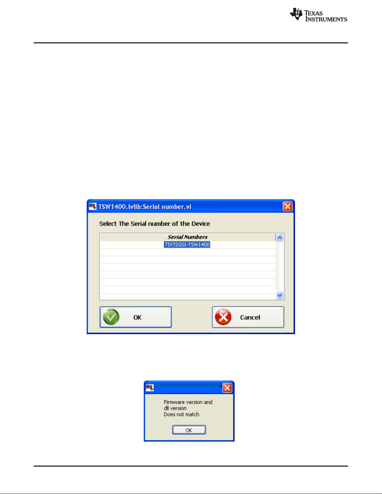
The TSW1400 GUI will first attempt to connect to the EVM USB interface. If the GUI identifies a valid
board serial number, a pop-up will open displaying this value, as shown in Figure 2. The serial number will
also have an EVM type number attached to it. This indicates to the GUI which of the three TSW140x
boards is being used. It is possible to connect several TSW1400 EVM’s to one host PC but the GUI can
only connect to one at a time. In the case were multiple boards are connected to the PC, the pop-up will
display all of the serial numbers found. It is then up to the user to select which board the GUI will be
associated.
www.ti.com
Figure 2. TSW1400EVM Serial Number
Click on “OK” to connect the GUI to the board. If the FPGA firmware version read by the GUI does not
match the firmware to be used as determined by the device selected, the following message will appear
as shown in Figure 3. This message also appears after power up as the FPGA is not programmed.
Figure 3. Firmware Does Not Match the Device Selected
8
TSW140x High Speed Data Capture/Pattern Generator Card SLWU079– February 2012
Copyright © 2012, Texas Instruments Incorporated
Submit Documentation Feedback
Page 9
www.ti.com
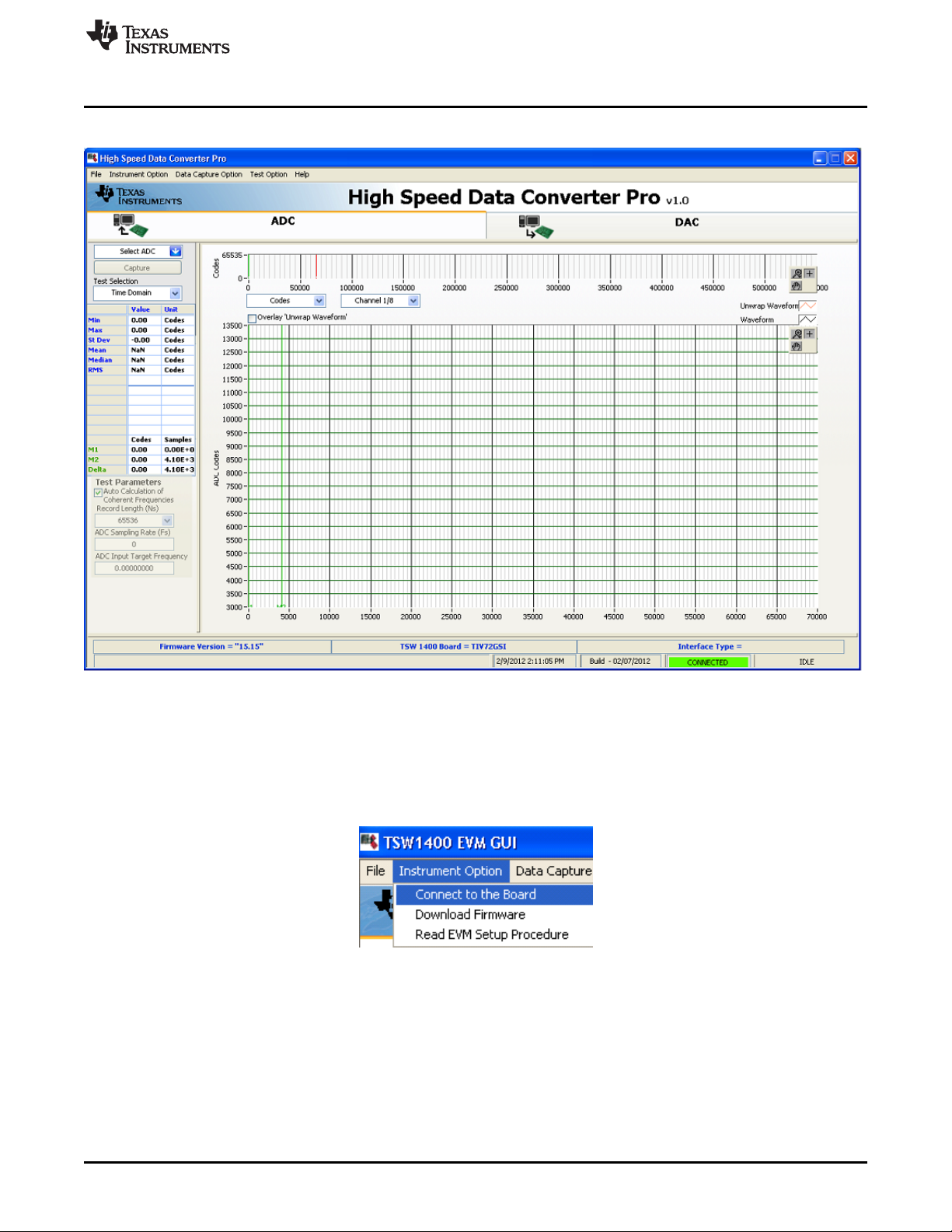
Click on “OK”. The Top level GUI will now open and appear as shown in Figure 4.
Software Start up
Figure 4. TSW1400EVM GUI Top Level
After the software has established a connection, if the message “Board not Connected” opens, double
check the USB cable connections and that power switch SW7 is in the “ON” position. If the cable
connections appear fine, try establishing a connection by clicking on the “Instrument Option” tab at the top
left of the GUI and select “Connect to the Board” (see Figure 5). If this still does not correct this issue,
check the status of the host USB port.
Figure 5. Connecting GUI to EVM
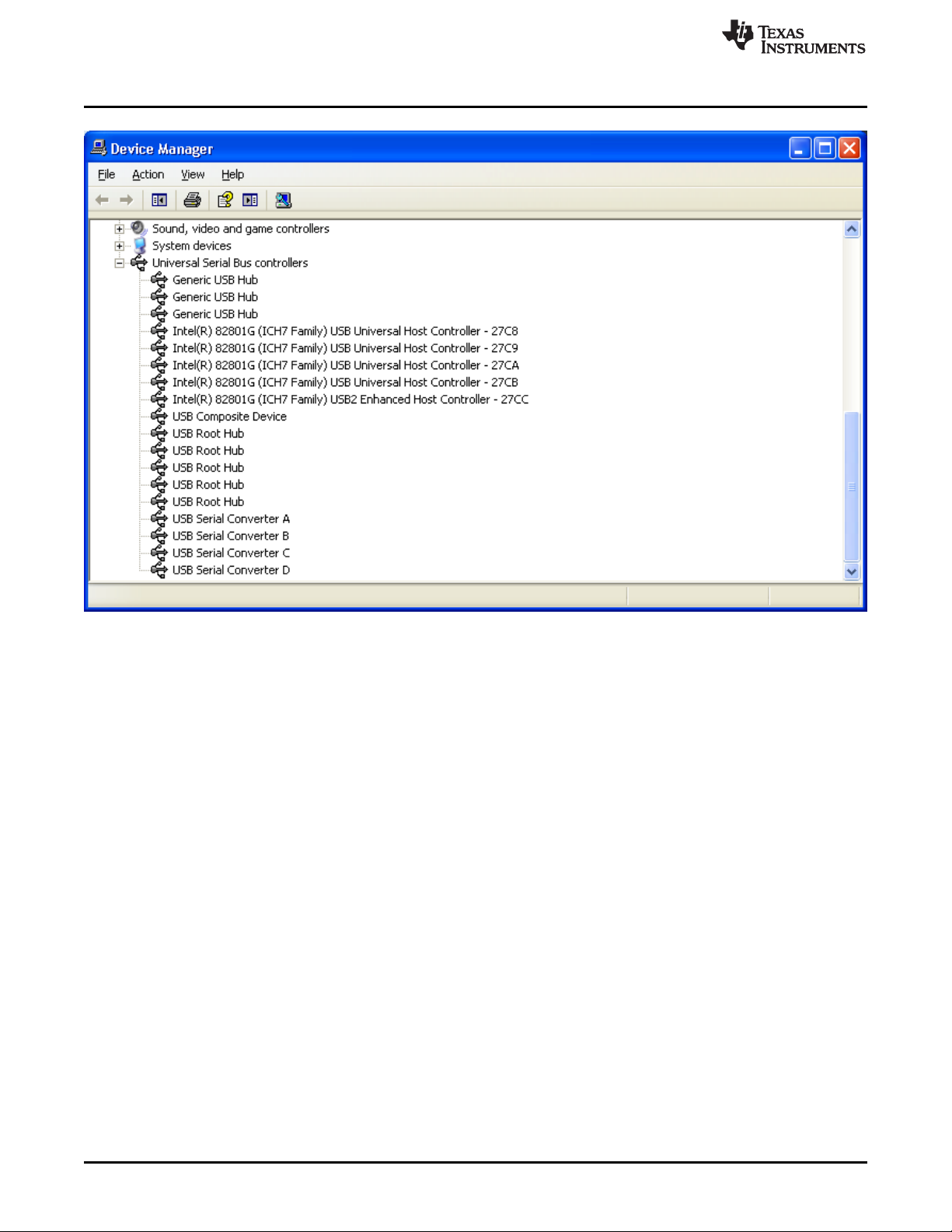
When the software is installed and the USB cable has been connected the TSW1400EVM and the PC, the
TSW1400 USB serial converter should be located in the Hardware Device Manager under the Universal
Serial Bus controllers as shown in Figure 6. This is a quad device which is why there is an A, B, C, and D
USB Serial Converter shown. When the USB cable is removed, these four will no longer be visible in the
Device Manager. If the drivers are present in the Device Manager window and the software still does not
connect, cycle power to the board and repeat the steps above.
SLWU079– February 2012 TSW140x High Speed Data Capture/Pattern Generator Card
Submit Documentation Feedback
Copyright © 2012, Texas Instruments Incorporated
9
Page 10
User Interface
www.ti.com
3.3 Device ini Files
Included in the installation for the TSW1400 GUI software is a subdirectory of ini files for each category of
ADC and DAC that is supported by the TSW1400EVM. TI strongly recommends that these files are not
edited except at the factory. These files contain necessary information for the GUI software to properly
configure the TSW1400EVM FPGA registers for proper operation with the desired ADC or DAC EVM.
Some of the entries within the ini file are obvious, such as defining the bit resolution for a device to be 11,
12, 14, or 16 bits. Other entries in the ini file define for the FPGA which LVDS pairs within the Samtec
connector define the data bus, and correct operation may not be possible if these entries are edited. The
use of ini files allows for new device types to be supported by the TSW1400EVM as they become
available without having to modify, re-release, or re-install the TSW1400 GUI software. New device types
may be supported at a later date simply by adding a new ini file to the proper subdirectory. This file can be
found on the TI website under the TSW1400 product folder.
4 User Interface
When the TSW1400 GUI software is started, the initial setup screen of Figure 4 appears. The
TSW1400EVM serial number is reported in the lower center of the GUI. After the FPGA is loaded with the
selected firmware, the GUI would reports the firmware version in the bottom left and the interface type will
be reported in the lower right. The connection status should read “Connected” and be highlighted in green
(lower center of the GUI). The status pane, located in the lower right, will report “IDLE”. Many of the
TSW1400 software controls are available from the main screen, such as “ADC or DAC” mode, “Select
device”, “Capture and Test Selection” (ADC mode only), and “Load File to transfer to TSW1400” (DAC
mode only).
Figure 6. Hardware Device Manager
10
TSW140x High Speed Data Capture/Pattern Generator Card SLWU079– February 2012
Copyright © 2012, Texas Instruments Incorporated
Submit Documentation Feedback
Page 11
www.ti.com
4.1 Toolbar
The toolbar contains options and settings that are independent of the device selected for test or the test to
be performed, such as configuration options and save/recall operations. The operations available under
the toolbar are grouped in categories as follows: File, Instrument Option, Data Capture Option, Test
Option and Help.
4.1.1 File Options
The file tab contains all of the options for saving or importing test results. Placing the mouse indicator over
the File tab will open a window with the available options as shown in Figure 7.
There are options for saving the ADC captured data as CSV or Binary format in a directory specified by
the user for export or archival purposes. The “Save as CSV File” and “Save as Binary File” will save the
results that are displayed in the test window. If the Single Tone FFT test is active, then the FFT plot will be
saved, along with the performance statistics and setup information. If the Time Domain test is active, then
the Time Domain plot will be saved along with the time domain statistics. The “Save Screen shot as “
option, when selected, will open a window that will allow the user to save the current GUI screen shot as
either a bmp, jpeg, or png file in the directory specified by the user.
The GUI provides an option to use simulated input data in place of an actual ADC evm. To use this
feature, select ‘Simulate ADC” in the device selection drop down. Click on the “Capture” button. A new
window will open asking for an input test file. This file must be in text format having integer values from
-32768 to 32767, one column per channel, and will be used by the GUI as input data for display and
analysis. For two channel test cases, this file must be 16 bit interleaved binary data, where channel 1 is
the first sample and channel 2 is the second sample.
User Interface
Figure 7. File Tab Options
4.1.2 Instrument Options
The Instrument Options menu tab contains four options: Reinitialize Instrument, Read EVM Setup
Procedure, Download Firmware, and Connect to the Board as shown in Figure 8.
Figure 8. Instrument Options
The Read ADC EVM Setup Procedure command causes the TSW1400 software to read a comment string
from the ini file for the device that is currently selected and then display that comment string in the status
pane. This comment string generally contains necessary setup information pertaining to the EVM under
test, such as possibly requiring a non-default data format or required jumper setting for the EVM to
communicate properly with the TSW1400EVM.
SLWU079– February 2012 TSW140x High Speed Data Capture/Pattern Generator Card
Submit Documentation Feedback
Copyright © 2012, Texas Instruments Incorporated
11
Page 12

User Interface
The Download Firmware command allows the user to select a file that will be used to program the FPGA.
These files need to be .rbf files for this to work. The files used by the GUI currently reside in the directory
called ”Firmware”, under the TSW1400 directory. This option would be used if the GUI cannot identify the
firmware file called out in the ini file, or if an advanced user has a new file they would like to try.
The Connect to the Board command will cause the GUI to read the serial number inside the USB
controller on the TSW1400 and display the value found or report that no board is connected. This can be
used when a user removes power from the TSW1400 board, then re-applies power while leaving the GUI
active.
4.1.3 Data Capture Option
The Data Capture Option (ADC mode only) has two options: Capture Option or Trigger Option (currently
not supported). Selecting Capture Option opens a new window as shown in Figure 9.
www.ti.com
The user can adjust the number of samples to capture from 4096 to 524,288. The GUI will round down to
the nearest multiple of 4096 and display this value. This captured data will be displayed in the codes
graph of the main screen as another method of letting the user know how many samples of data has been
collected. This number will set the maximum size that can be used for the Record Length value on the
main window. When Continuous Capture option is selected, the GUI will keep performing data captures
and displaying the results.
4.1.4 Test Option
The Test Option menu tab allows for setting the parameter options for the Single Tone FFT test, notch
frequency bins, Cursor Locks, an option to display 2 channels, and a dBFs/dBc display option as shown in
Figure 10.
Figure 9. Capture Option
Figure 10. Test Options
12
TSW140x High Speed Data Capture/Pattern Generator Card SLWU079– February 2012
Copyright © 2012, Texas Instruments Incorporated
Submit Documentation Feedback
Page 13

www.ti.com
4.1.4.1 dBFs
When selected, SNR, SFDR, and SINAD results will be display in dBFs. When not selected, the results
will be displayed in dBc.
4.1.4.2 Notch Frequency Bins
The Notch Frequency Bins option allows the user to remove a number of bins from the SNR calculation of
the input frequency around the fundamental, DC and a predetermined number of harmonics. The default
values for these settings when the capture is using rectangular mode is 0, 0, 1, 5, as shown in Figure 11.
When the capture mode is set to windowing, the default values are 5, 5, 5, 5.
User Interface
Figure 11. Notch Frequency Bin removal
By default, the noise calculations for SNR and SINAD are based on the FFT of the captured data with the
Notch Filter parameters applied. The first FFT bin at DC is not used because the first bin contains DC
offset and thus does not effect AC parameters or Ac performance. The rest of the FFT bins out to the
Nyquist frequency are included in the calculation of the total nois
e.
4.1.4.3 2 Channel Display and Cursor Lock
If the 2 channel display option is selected, a second data capture display window will open (Figure 12).
The user can now use this window to display the same channel but a different parameter, or a different
channel if a multi-channel ADC is under test. To remove the second channel display and go back to a
single channel display, click on this option again to remove the selected check mark.
SLWU079– February 2012 TSW140x High Speed Data Capture/Pattern Generator Card
Submit Documentation Feedback
Copyright © 2012, Texas Instruments Incorporated
13
Page 14
User Interface
www.ti.com
When 2 channels are displayed, if Cursor lock is enabled, the cursors in the lower display will be locked to
the ones in the upper display.
4.1.5 Help
Clicking on the help tab will open a window with three options. The first option, labeled "About", will open a
status window displaying the current version of the GUI, the software DLL, and the loaded firmware.
The second option labeled "Degug Support", will enable a debug email option. With this option enabled, if
a GUI error occurs, the software will prompt the user that it is emailing a debug log to a TI support team.
For every subsequent error until the user disbales this feature, the GUI will silently send the log file. The
third option, labeled "TSW1400 Help", opens a window displaying the contents of the User's Guide,
allowing the user to search for topics regarding the operation of the GUI.
4.2 Status Windows
The TSW1400 GUI reports system status such as downloading, capturing, warnings, errors, and
informational output in several locations. In the lower right portion of the screen, when the GUI is loading
the FPGA, loading data to memory, or performing a data capture, a rolling bar will appear in place of the
IDLE message. A new window will also open in the middle of the screen describing what the GUI is
currently doing. An example showing these status windows during a firmware load is shown in Figure 13.
Figure 12. Two Channel Display
14
TSW140x High Speed Data Capture/Pattern Generator Card SLWU079– February 2012
Copyright © 2012, Texas Instruments Incorporated
Submit Documentation Feedback
Page 15

www.ti.com
During operation of the TSW1400 software, warnings may appear in the center status window if selections
made from the drop-down menus of the interface are incompatible with the hardware selections or
settings. For example, if a sample rate is entered that is faster than that supported by a particular ADC
data sheet, a warning will appear as shown in Figure 14.
User Interface
Figure 13. Status Window
4.3 Mode Selection
The first selection a user needs to make is to select the type of EVM that is to be tested with the
TSW1400 EVM. The user will click on either the “ADC” or “DAC” button located at the top of the GUI as
shown in Figure 15.
The mode selected will determine the main screen format. When ADC is selected, the GUI will be setup
for displaying ADC data capture results. If DAC is selected, the GUI will setup controls to load a test
pattern, create a test pattern, and display the graphical representation of the test pattern to be sent to a
DAC EVM once the file has been read by the GUI.
4.4 Device Selection
After the board mode has been set, the user needs to select the device to be tested from the device
selection drop-down menu. If the GUI is in ADC mode, clicking on the drop down arrow will display the
ADC options available, as shown in Figure 16. If in DAC mode, the list will display available DAC’s.
Figure 14. Center Status Window
Figure 15. TSW1400 Modes
SLWU079– February 2012 TSW140x High Speed Data Capture/Pattern Generator Card
Submit Documentation Feedback
Copyright © 2012, Texas Instruments Incorporated
15
Page 16

User Interface
www.ti.com
Figure 16. ADC Device Selection Window
Each device that has an ini file installed in the proper directory automatically has an entry in the device
selection drop-down menu.
4.5 Capture Button (ADC Mode only)
The Capture button initiates a data capture once all other selections are made. The data capture can be a
single capture and display, or a continuous repeating capture (Data Capture Option tab in Tool Bar).
When continuous capture is enabled, this button display will change from “Capture” to “Stop”. Clicking on
this mode when in this mode will stop the continuous capture.
4.6 Test Selection (ADC Mode only)
The Test Selection drop-down has options for displaying data as a Time Domain, Single Tone, Two Tone,
or ACPR. The Single Tone FFT displays the power spectrum of the captured data with calculated AC
performance statistics. Time Domain displays the raw captured data in the format of a logic analyzer
display and output level over time. Two tone mode sets up cursors and displays results normally used with
this type of testing. ACPR is currently not supported with this release.
16
TSW140x High Speed Data Capture/Pattern Generator Card SLWU079– February 2012
Copyright © 2012, Texas Instruments Incorporated
Submit Documentation Feedback
Page 17

www.ti.com
4.6.1 Single Tone FFT
The Single Tone FFT screen is shown in Figure 17. The larger central pane displays the FFT power
spectrum, whereas the calculated statistics are grouped into categories on the left side of the screen.
Settings and inputs relevant to the test are entered in drop-down menus or text input boxes on the bottom
left portion of the window.
The red horizontal line shown is the RMS line. This line indicates the RMS average of the noise floor of
the FFT plot. The RMS average is computed over all of the FFT bins except the bin containing the
input frequency. More precisely, the RMS line = SINAD + FFT Record Length Process Gain where
FFT Record Process Gain = 10log(number of points/2).
.
User Interface
Figure 17. Single Tone FFT Display
4.6.1.1 Parameter Controls
The sampling rate is entered in the ADC Sampling Rate text box, also called the Sampling Frequency
(FS). The number is entered in Hertz (Hz), although the letter M may be appended to represent the
sampling rate in MHz. For example, 125 M = 125 MHz or 125,000,000 Hz.
The expected input frequency is entered in the ADC Input Target Frequency panel. If the Auto Calculation
of Coherent Input Frequency mode is enabled, then this input frequency is adjusted up or down slightly
away from the input frequency automatically. If coherent input frequency is required, the signal generator
used to source the input frequency must be set to this exact calculated coherent frequency. The coherent
frequency calculation takes the sampling frequency, the input frequency as entered by the user, and the
FFT record length and adjusts the input frequency so that the captured data starts and ends on the same
place of the sine wave of the input frequency. This avoids an artifact of the FFT calculation from
presenting a smeared power spectrum due to the fact that the FFT presumes the sample of the input is
part of a continuous input signal. If the input and sampling frequency is not coherent, and the sampled
SLWU079– February 2012 TSW140x High Speed Data Capture/Pattern Generator Card
Submit Documentation Feedback
Copyright © 2012, Texas Instruments Incorporated
17
Page 18

User Interface
data is appended end to end to form a continuous input signal, then there is an apparent phase
discontinuity at the beginning and the end of the sampled data. Making the sampling and input
frequencies coherent avoids this apparent discontinuity. If the input frequency cannot be made coherent,
then the windowing functions other than Rectangular can be used to process out this effect to some
degree.
The FFT record length can be set in the Record Length (NS) panel. The TSW1400EVM supports FFT
record lengths of as much as 524288 samples, or as little as 4096 samples. The red vertical line shown in
the codes graph represents where the last sample is used from the captured data. The GUI will only allow
record lengths that are the same size or smaller than the number of captured samples.
4.6.1.2 ADC Captured Data Display Pane
The ADC captured data is displayed in the major center portion of the GUI. The data display panel has
three display control drop-downs. The data type drop-down, allows the user to display the results as
Frequency, Codes, or Bits as shown in Figure 18.
www.ti.com
Figure 18. Data Display Options
The Codes option will display the data as actual digital codes. The Bit option will show the values of the
individual ADC output bits and displayed as if it were captured by a logic analyzer.
The Channel drop-down selects which channel of a multi-channel ADC is to be displayed as shown in
Figure 19.
Figure 19. Channel Selection Window
The GUI provides a windowing function to be applied to ADC captured data. .In the Window Display
drop-down menu (Figure 20), Rectangular Window applies a unity gain to all data points of the captured
data. A Hanning Window, Hamming Window, or Blackman-Harris Window function can be applied to the
captured data for situations where the sample rate and the input frequency are not or cannot be set
precisely to capture an integer number of cycles of the input frequency (sometimes called coherent
frequency).
18
Figure 20. Data Windowing Options
TSW140x High Speed Data Capture/Pattern Generator Card SLWU079– February 2012
Copyright © 2012, Texas Instruments Incorporated
Submit Documentation Feedback
Page 19

www.ti.com
4.6.1.3 FFT Power Spectrum
The FFT power spectrum of the captured data is displayed in the major center portion of the window. The
TSW1400 software automatically scales the horizontal axis from DC through the Nyquist frequency,
although the scale of the horizontal axis can be changed simply by highlighting the text and typing in a
new value. For example, the display in Figure 10 can be used to zoom in on the input frequency by
highlighting the 0 MHz at the end of the spectrum and typing 25 M, and then highlighting the 60M and
typing in 35 M. This causes the portion of the power spectrum from 25 MHz through 35 MHz to fill the
power spectrum display.
The vertical scale of the power spectrum is automatically scaled to display the noise floor of the FFT result
up through 0 dBFS. The vertical scale can also be manually adjusted by highlighting the limits of the
vertical scale and typing in new limits. By default, the first few harmonics of the input frequency are
marked in the display, as well as an additional marker that can be placed by dragging the marker to any
place in the power spectrum, such as a noise spur that is not already marked as a harmonic. By default
this additional marker initially goes to the highest spur that is not identified as a harmonic.
Display properties can be edited by using the mouse to right-click in the power spectrum display. Visible
properties such as the graph palette or plot legend can be edited, and auto-scale of the vertical and
horizontal axis’s can be enabled or not.
4.6.1.4 Overlay Unwrap Waveform
The Overlay Unwrap Waveform check box, located near the top left section of the captured display, allows
a calculated normalized waveform to be overlaid (in red) over the sample data waveform (in black). If the
sample and input frequencies are coherent, the sampled data is normalized into a calculated
representation of a single period of a sine wave. Errors in the sampled data for any reason become
immediately apparent as spikes on the unwrapped waveform.
User Interface
4.6.1.5 Single FFT Statistics
For the Single FFT test, a number of calculated statistics and AC performance measurements are
displayed to the left of the power spectrum display.
SNR - Signal-to-Noise Ratio is the ratio of the power of the fundamental (PS) or input frequency to the
noise floor power (PN), excluding the power at DC and the first five harmonics. SNR is either given in
units of dBc (dB to carrier) when the absolute power of the fundamental is used as the reference, or
dBFS (dB to full scale) when the power of the fundamental is extrapolated to the converter’s full-scale
range.
SNR = 10Log10(Ps/Pn (1)
SFDR - Spurious-Free Dynamic Range is ratio of the power of the fundamental to the highest other
spectral component (either spur or harmonic). SFDR is typically given in units of dBc (dB to carrier).
THD - Total Harmonic Distortion is the ratio of the power of the fundamental (PS) to the power in the
first five harmonics (PD). THD is typically given in data sheets in units of dBc (dB to carrier).
SINAD - Signal-to-Noise and Distortion is the ratio of the power of the fundamental (PS) to the power
of all the other spectral components including noise (PN) and distortion (PD), but excluding DC.
SINAD = 10Log10(Ps/(Pn+Pd)) (2)
ENOB - Effective Number of Bits is a measure of a converter’s performance as compared to the
theoretical limit based on quantization noise.
ENOB = (SINAD-1.76)/6.02 (3)
Fund. – This parameter displays the power level of the fundamental.
Worst Spur. - This parameter displays the power level of the worst spur.
HD2-6 – Display the power values of the second through sixth harmonics of the input frequency in dBc.
M1, M2, Delta – Displays the power level of the location of markers M1 and M2. These markers can be
moved around on the spectrum with the mouse. The Delta parameter displays the power difference
between M2 and M1.
SLWU079– February 2012 TSW140x High Speed Data Capture/Pattern Generator Card
Submit Documentation Feedback
Copyright © 2012, Texas Instruments Incorporated
19
Page 20

User Interface
4.6.2 Time Domain
The Time Domain option, when selected, will display the ADC captured data as digital codes in the time
domain. The statistics of the codes reported on the left side of the GUI are minimum value (Min),
maximum value (Max), Standard deviation (St. Dev), Mean, Median, and RMS.
M1, M2, Delta – Displays the code value of the location of markers M1 and M2. These markers can be
moved around on the display with the mouse. The Delta parameter displays the power difference between
M2 and M1.
4.6.3 Two Tone
The Two Tone option, when selected, will display a two tone ADC captured with markers placed at the
locations specified by the user. The statistics of the captured data reported on the left side of the GUI are
as follows:
F1 - This parameter displays the power level of the first fundamental.
F2 - This parameter displays the power level of the second fundamental.
2F1+F2 - This parameter displays the power level at the frequency that is equal to twice the first
fundamental plus the second fundamental.
2F2+F1 - This parameter displays the power level at the frequency that is equal to twice the second
fundamental plus the first fundamental. The other parameters follow this format.
A new window opens on the bottom left of the GUI for entering the second ADC input frequency,
Figure 21.
www.ti.com
4.6.4 ACPR
The ACPR option, when selected, will display the Adjacent Channel power of the captured data. This
function is currently not supported.
20
TSW140x High Speed Data Capture/Pattern Generator Card SLWU079– February 2012
Figure 21. ADC 2nd Input Frequency Box
Copyright © 2012, Texas Instruments Incorporated
Submit Documentation Feedback
Page 21

www.ti.com
4.7 DAC Display Panel (DAC Mode only)
Selecting the “DAC” button at the top right of the GUI main panel will change the panel display mode for
DAC operation as shown in Figure 22.
User Interface
Figure 22. DAC Display Mode
4.7.1 Send Button (DAC Mode only)
This button, located in the upper left side of the GUI, will cause the GUI to download data to the TSW1400
on-board memory, followed by the TSW1400 sending data from the memory module to the DAC EVM
under test. This button is only active after valid data has been loaded into the PC memory by the GUI.
4.7.2 Load File Button
The button labeled “Load File to transfer into TSW1400” is used to select the test pattern file to be loaded
into the board memory. Clicking on this button will open a navigator which the user will use to select the
desired test file. The format of the test file is .csv. Once selected, the file will be loaded into the PC
memory used by the GUI.
The imported file must be text format integer value from -32768 to 32767 in a single column format if
testing a single DAC. For dual DAC’s, the file must be in 2 columns. For quad DAC’s, 4 columns. The
length can be from 4096 to 512M (single column) in increments of 32. The GUI comes with several
example test files that can be found under the following directory: C:\Program Files\Texas
Instruments\High Speed Data Converter Pro\TSW1400 Details\Testfiles.
SLWU079– February 2012 TSW140x High Speed Data Capture/Pattern Generator Card
Submit Documentation Feedback
Copyright © 2012, Texas Instruments Incorporated
21
Page 22

User Interface
4.7.3 Parameter Controls
Four parameters are used with the data file to generate the Time and Frequency domain plots.
Preamble – The number of samples before the loop starting point (default is 0). This value must be in
increments of 32.
Data Rate – Sample rate of I/Q samples of the test file. This is only used by the GUI FFT frequency
display graph. The number is entered in Hertz (Hz), although the letter M may be appended to
represent the sampling rate in MHz.
DAC Option – Determines if the test pattern file is either 2's Compliment or Offset Binary.
Active Channel – Selects the channel in the test pattern file that is displayed (1, 2, 3, or 4).
After a file has been loaded and the parameters updated, the GUI panel will present a graphical
representation of the data. An example of an Offset Binary, 25.1 MHz tone with a data rate of 250MHz is
shown in Figure 23.
www.ti.com
22
Figure 23. DAC Test Pattern Display
The “Send” button will now became active. Clicking on this button will start the transfer of data from the
TSW1400 to a DAC EVM under test. This pattern is a looping test pattern that constantly runs until the
send button is clicked on again.
TSW140x High Speed Data Capture/Pattern Generator Card SLWU079– February 2012
Copyright © 2012, Texas Instruments Incorporated
Submit Documentation Feedback
Page 23

www.ti.com
4.8 I/Q Multi-tone Generator
Located in the lower left corner of the GUI is an I/Q Multi-tone Generator tool that allows the user to
generate test patterns that can be used with the TSW1400 GUI. The following parameters are used with
this tool:
Tone BW – Tone bandwidth in Megahertz.
# - Number of tones. If set to 1, Tone BW will be ignored.
Tone Center – Center frequency of tones in Megahertz.
# of Samples – Number of test samples. 4096 to 2M, in increments of 32.
Tone Selection – Real or I/Q.
Scaling Factor (1X) – From full scale output. 0.0000 to 1.0000.
To generate a pattern, enter the desired parameters then click on the button labeled “Create Tones”. Click
on “Send” will send the data to the TSW1400 memory then to the DAC EVM under test. An option exist to
allow the user to save this file as well.
5 ADC Data Capture Software Operation
5.1 Testing with an ADS5281 EVM
This section describes the operation when testing with an ADS5281 EVM that has a LVDS output
interface.
• Power down the TSW1400 if an ADC evm is not installed.
• Connect J8 of the ADS5281 EVM to connector J3 of the TSW1400.
• Provide unpowered +5 VDC connections to J1 and return to J2 of the ADS5281 EVM.
• Provide a 1.5 VPP 50 MHz sine-wave clock to J26 of the ADS5281 EVM.
• Provide a filter 5 MHz analog input to CH1.
• Power up the TSW1400 followed by the ADC evm.
• Start up the TSW1400 GUI as described in the Software Start Up section.
• The TSW1400 EVM connected to an ADS5281 EVM is shown in Figure 24
ADC Data Capture Software Operation
SLWU079– February 2012 TSW140x High Speed Data Capture/Pattern Generator Card
Submit Documentation Feedback
Copyright © 2012, Texas Instruments Incorporated
23
Page 24

ADC Data Capture Software Operation
www.ti.com
Figure 24. TSW1400EVM interfacing to an ADS5281 EVM
To setup the GUI to run in the data capture mode, click on the “ADC” tab in the top left side of the GUI.
Navigate to the device selection button located in the upper left side of the GUI, click on the drop down
arrow, then select “ADS5281”. After double clicking on this file, a pop-up will open asking “Do you want to
update the Firmware for ADC”. Click on “Yes”. The firmware will now start loading and take ~ 20 seconds
to complete. After the ADS5281 firmware load has completed, the FPGA_CONF_DONE LED will turn on
after the FPGA configured. The LED’s labeled USER_LED (0-7) will also be on except for USER_LED4.
NOTE: If the TSW1400 is not receiving a valid clock from the ADC EVM, USER_LED3 will be off.
• Use the “Test Selection” button to change the capture display to Single Tone.
• Set the active channel setting to Channel 1/8.
• Use the default Record Length value of 65,536.
• Set the ADC Sampling Rate to 50 MHz.
• Click on the Auto Calculation of Coherent Frequency function if using Rectangular capture mode.
• Set the input frequency source to the new value in ADC Input Target Frequency that is generated by
the Auto Calculation of Coherent Frequency function.
• Make sure the display mode is set to “Frequency”.
• Click on the “Capture” button to perform a data capture. The results should like similar to those shown
in Figure 25.
24
TSW140x High Speed Data Capture/Pattern Generator Card SLWU079– February 2012
Copyright © 2012, Texas Instruments Incorporated
Submit Documentation Feedback
Page 25

www.ti.com
ADC Data Capture Software Operation
Figure 25. ADC5281 Single Tone FFT Capture Results
The user can now change other parameters and do another capture to observe the ADC outputs with
different frequencies, amplitudes, and in other formats such as codes, or bits.
After the firmware is loaded, if the user clicks the drop down arrow in the device selection window, the GUI
will indicate which ADC EVM’s can be used with this firmware load by adding a black diamond in front of
the device name, as shown in Figure 26. If the user does not power down the TSW1400, any one of the
devices with a black diamond can be tested without doing another firmware load.
SLWU079– February 2012 TSW140x High Speed Data Capture/Pattern Generator Card
Submit Documentation Feedback
Copyright © 2012, Texas Instruments Incorporated
25
Page 26

ADC Data Capture Software Operation
www.ti.com
Figure 26. Devices Supported with Current Firmware Load
WARNING
After testing is completed, always close the GUI before
disconnecting the USB cable between the host PC and EVM.
Failure to do this can cause a blue screen reboot to occur on the
host PC.
26
TSW140x High Speed Data Capture/Pattern Generator Card SLWU079– February 2012
Copyright © 2012, Texas Instruments Incorporated
Submit Documentation Feedback
Page 27

www.ti.com
6 TSW1400 Pattern Generator Operation
6.1 Testing with DAC3152 EVM
This section describes the pattern generator operation when testing with a DAC3152 EVM that has a
LVDS input interface.
• Power down the TSW1400.
• Connect J5 of the DAC3152 EVM to connector J4 of the TSW1400.
• Provide +5 VDC to J12 and return to J13 of the DAC3152 EVM.
• Provide a 0.5-Vrms 250 MHz clock to J9 of the DAC3152 EVM.
• Power up the TSW1400 EVM
• Start up the TSW1400 GUI as described in the Software Start Up.
• A TSW1400 EVM connected to a DAC3152 EVM is shown in Figure 27.
TSW1400 Pattern Generator Operation
Figure 27. TSW1400 EVM Interfacing to a DAC EVM
NOTE: The FPGA clocks from DAC EVM’s to the TSW1400 EVM have to be LVDS level. Exceeding
LVDS levels may damage the TSW1400 FPGA.
6.2 Loading DAC Firmware
If opening the GUI for the first time, when setting up for pattern generator mode, make sure “DAC” in the
top right side of the GUI is selected. After clicking on “DAC”, the top level GUI shall look as shown in
Figure 28.
SLWU079– February 2012 TSW140x High Speed Data Capture/Pattern Generator Card
Submit Documentation Feedback
Copyright © 2012, Texas Instruments Incorporated
27
Page 28

TSW1400 Pattern Generator Operation
www.ti.com
Figure 28. TSW1400EVM GUI DAC Mode Top Level
To run the GUI in DAC pattern generator mode, the FPGA must be loaded with the proper firmware, which
is determined by the DAC type to be tested.
In the “Select DAC” button of the GUI, click on the drop down arrow and select the DAC3152 (Figure 29).
This will be the targeted EVM for this test example.
Figure 29. DAC Selection
Click on “Yes” when asked “Do you want to update the firmware for DAC”. The firmware for this setup will
now be loaded during this process, which will take ~ 20 seconds. After the firmware load has completed,
the LED’s labeled USER_LED (0-7) will now turn on except for USER_LED 3 and 5. USER_LED 3 is used
to indicate the status of a second PLL, which is not used with this firmware build, and USER_LED 5
indicates if there is a FIFO overflow (error) of the transmit data.
NOTE: If the TSW1400 is not receiving a valid clock from the DAC evm, USER_LED3 and
USER_LED4 will be off.
28
TSW140x High Speed Data Capture/Pattern Generator Card SLWU079– February 2012
Copyright © 2012, Texas Instruments Incorporated
Submit Documentation Feedback
Page 29

www.ti.com
6.3 Configuring TSW1400 for Pattern Generation
For this test, at the top of the GUI, set the following parameters:
• Preamble to 0
• Data Rate – 250 MSPS
• DAC Option – Offset Binary
• Active Channel – Channel 1
• FFT Length – 32768
• Window - Rectangular
The pattern generation data file should match one of the Record Length’s to us the Rectangular window
mode. If it does not, switch the window mode to another setting such as “Hanning”.
• Click on the button labeled “Load File to transfer into TSW1400”.
• Select “single_tone_cmplx_32768_250MSPS_BW_25.1MHZ.csv”.
• Click on “Send”.
The display panel of the GUI will be updated, showing the test data that will be transmitted to the DAC
EVM in both codes and frequency domain as shown in Figure 30.
TSW1400 Pattern Generator Operation
Figure 30. TSW1400 Output Data to DAC EVM
Using a spectrum analyzer, verify that there is now a 25.1 MHz tone present on both SMA J2 (IOUTA2)
and J3 (IOUTB2) of the DAC3152 EVM.
To shut down the GUI, click on the “File” tab in the upper right corner of the GUI and select “Exit” in the
pop up window that opens. This will specify that the USB ports are released by the software.
SLWU079– February 2012 TSW140x High Speed Data Capture/Pattern Generator Card
Submit Documentation Feedback
Copyright © 2012, Texas Instruments Incorporated
29
Page 30

EVALUATION BOARD/KIT/MODULE (EVM) ADDITIONAL TERMS
Texas Instruments (TI) provides the enclosed Evaluation Board/Kit/Module (EVM) under the following conditions:
The user assumes all responsibility and liability for proper and safe handling of the goods. Further, the user indemnifies TI from all
claims arising from the handling or use of the goods.
Should this evaluation board/kit not meet the specifications indicated in the User’s Guide, the board/ kit may be returned within 30
days from the date of delivery for a full refund. THE FOREGOING LIMITED WARRANTY IS THE EXCLUSIVE WARRANTY MADE
BY SELLER TO BUYER AND IS IN LIEU OF ALL OTHER WARRANTIES, EXPRESSED, IMPLIED, OR STATUTORY,
INCLUDING ANY WARRANTY OF MERCHANTABILITY OR FITNESS FOR ANY PARTICULAR PURPOSE. EXCEPT TO THE
EXTENT OF THE INDEMNITY SET FORTH ABOVE, NEITHER PARTY SHALL BE LIABLE TO THE OTHER FOR ANY
INDIRECT, SPECIAL, INCIDENTAL, OR CONSEQUENTIAL DAMAGES.
Please read the User's Guide and, specifically, the Warnings and Restrictions notice in the User's Guide prior to handling the
product. This notice contains important safety information about temperatures and voltages. For additional information on TI's
environmental and/or safety programs, please visit www.ti.com/esh or contact TI.
No license is granted under any patent right or other intellectual property right of TI covering or relating to any machine, process, or
combination in which such TI products or services might be or are used. TI currently deals with a variety of customers for products,
and therefore our arrangement with the user is not exclusive. TI assumes no liability for applications assistance, customer product
design, software performance, or infringement of patents or services described herein.
REGULATORY COMPLIANCE INFORMATION
As noted in the EVM User’s Guide and/or EVM itself, this EVM and/or accompanying hardware may or may not be subject to the
Federal Communications Commission (FCC) and Industry Canada (IC) rules.
For EVMs not subject to the above rules, this evaluation board/kit/module is intended for use for ENGINEERING DEVELOPMENT,
DEMONSTRATION OR EVALUATION PURPOSES ONLY and is not considered by TI to be a finished end product fit for general
consumer use. It generates, uses, and can radiate radio frequency energy and has not been tested for compliance with the limits of
computing devices pursuant to part 15 of FCC or ICES-003 rules, which are designed to provide reasonable protection against
radio frequency interference. Operation of the equipment may cause interference with radio communications, in which case the
user at his own expense will be required to take whatever measures may be required to correct this interference.
General Statement for EVMs including a radio
User Power/Frequency Use Obligations: This radio is intended for development/professional use only in legally allocated frequency
and power limits. Any use of radio frequencies and/or power availability of this EVM and its development application(s) must
comply with local laws governing radio spectrum allocation and power limits for this evaluation module. It is the user’s sole
responsibility to only operate this radio in legally acceptable frequency space and within legally mandated power limitations. Any
exceptions to this is strictly prohibited and unauthorized by Texas Instruments unless user has obtained appropriate
experimental/development licenses from local regulatory authorities, which is responsibility of user including its acceptable
authorization.
For EVMs annotated as FCC – FEDERAL COMMUNICATIONS COMMISSION Part 15 Compliant
Caution
This device complies with part 15 of the FCC Rules. Operation is subject to the following two conditions: (1) This device may not
cause harmful interference, and (2) this device must accept any interference received, including interference that may cause
undesired operation
Changes or modifications not expressly approved by the party responsible for compliance could void the user's authority to operate
the equipment.
FCC Interference Statement for Class A EVM devices
This equipment has been tested and found to comply with the limits for a Class A digital device, pursuant to part 15 of the FCC
Rules. These limits are designed to provide reasonable protection against harmful interference when the equipment is operated in
a commercial environment. This equipment generates, uses, and can radiate radio frequency energy and, if not installed and used
in accordance with the instruction manual, may cause harmful interference to radio communications. Operation of this equipment in
a residential area is likely to cause harmful interference in which case the user will be required to correct the interference at his
own expense.
Page 31

REGULATORY COMPLIANCE INFORMATION (continued)
FCC Interference Statement for Class B EVM devices
This equipment has been tested and found to comply with the limits for a Class B digital device, pursuant to part 15 of the FCC
Rules. These limits are designed to provide reasonable protection against harmful interference in a residential installation. This
equipment generates, uses and can radiate radio frequency energy and, if not installed and used in accordance with the
instructions, may cause harmful interference to radio communications. However, there is no guarantee that interference will not
occur in a particular installation. If this equipment does cause harmful interference to radio or television reception, which can be
determined by turning the equipment off and on, the user is encouraged to try to correct the interference by one or more of the
following measures:
• Reorient or relocate the receiving antenna.
• Increase the separation between the equipment and receiver.
• Connect the equipment into an outlet on a circuit different from that to which the receiver is connected.
• Consult the dealer or an experienced radio/TV technician for help.
For EVMs annotated as IC – INDUSTRY CANADA Compliant
This Class A or B digital apparatus complies with Canadian ICES-003.
Changes or modifications not expressly approved by the party responsible for compliance could void the user’s authority to operate
the equipment.
Concerning EVMs including radio transmitters
This device complies with Industry Canada licence-exempt RSS standard(s). Operation is subject to the following two conditions:
(1) this device may not cause interference, and (2) this device must accept any interference, including interference that may cause
undesired operation of the device.
Concerning EVMs including detachable antennas
Under Industry Canada regulations, this radio transmitter may only operate using an antenna of a type and maximum (or lesser)
gain approved for the transmitter by Industry Canada. To reduce potential radio interference to other users, the antenna type and
its gain should be so chosen that the equivalent isotropically radiated power (e.i.r.p.) is not more than that necessary for successful
communication.
This radio transmitter has been approved by Industry Canada to operate with the antenna types listed in the user guide with the
maximum permissible gain and required antenna impedance for each antenna type indicated. Antenna types not included in this
list, having a gain greater than the maximum gain indicated for that type, are strictly prohibited for use with this device.
Cet appareil numérique de la classe A ou B est conforme à la norme NMB-003 du Canada.
Les changements ou les modifications pas expressément approuvés par la partie responsable de la conformité ont pu vider
l’autorité de l'utilisateur pour actionner l'équipement.
Concernant les EVMs avec appareils radio
Le présent appareil est conforme aux CNR d'Industrie Canada applicables aux appareils radio exempts de licence. L'exploitation
est autorisée aux deux conditions suivantes : (1) l'appareil ne doit pas produire de brouillage, et (2) l'utilisateur de l'appareil doit
accepter tout brouillage radioélectrique subi, même si le brouillage est susceptible d'en compromettre le fonctionnement.
Concernant les EVMs avec antennes détachables
Conformément à la réglementation d'Industrie Canada, le présent émetteur radio peut fonctionner avec une antenne d'un type et
d'un gain maximal (ou inférieur) approuvé pour l'émetteur par Industrie Canada. Dans le but de réduire les risques de brouillage
radioélectrique à l'intention des autres utilisateurs, il faut choisir le type d'antenne et son gain de sorte que la puissance isotrope
rayonnée équivalente (p.i.r.e.) ne dépasse pas l'intensité nécessaire à l'établissement d'une communication satisfaisante.
Le présent émetteur radio a été approuvé par Industrie Canada pour fonctionner avec les types d'antenne énumérés dans le
manuel d’usage et ayant un gain admissible maximal et l'impédance requise pour chaque type d'antenne. Les types d'antenne non
inclus dans cette liste, ou dont le gain est supérieur au gain maximal indiqué, sont strictement interdits pour l'exploitation de
l'émetteur.
Page 32

【Important Notice for Users of this Product in Japan】
This development kit is NOT certified as Confirming to Technical Regulations of Radio Law of Japan
If you use this product in Japan, you are required by Radio Law of Japan to follow the instructions below with respect to this
product:
1. Use this product in a shielded room or any other test facility as defined in the notification #173 issued by Ministry of Internal
Affairs and Communications on March 28, 2006, based on Sub-section 1.1 of Article 6 of the Ministry’s Rule for Enforcement of
Radio Law of Japan,
2. Use this product only after you obtained the license of Test Radio Station as provided in Radio Law of Japan with respect to
this product, or
3. Use of this product only after you obtained the Technical Regulations Conformity Certification as provided in Radio Law of
Japan with respect to this product. Also, please do not transfer this product, unless you give the same notice above to the
transferee. Please note that if you could not follow the instructions above, you will be subject to penalties of Radio Law of
Japan.
(address) 24-1, Nishi-Shinjuku 6 chome, Shinjukku-ku, Tokyo, Japan
http://www.tij.co.jp
【ご使用にあたっての注】
本開発キットは技術基準適合証明を受けておりません。
本製品のご使用に際しては、電波法遵守のため、以下のいずれかの措置を取っていただく必要がありますのでご注意ください。
1. 電波法施行規則第6条第1項第1号に基づく平成18年3月28日総務省告示第173号で定められた電波暗室等の試験設備でご使用い
ただく。
2. 実験局の免許を取得後ご使用いただく。
3. 技術基準適合証明を取得後ご使用いただく。
なお、本製品は、上記の「ご使用にあたっての注意」を譲渡先、移転先に通知しない限り、譲渡、移転できないものとします。
上記を遵守頂けない場合は、電波法の罰則が適用される可能性があることをご留意ください。
日本テキサス・インスツルメンツ株式会社
東京都新宿区西新宿6丁目24番1号
西新宿三井ビル
http://www.tij.co.jp
Texas Instruments Japan Limited
SPACER
SPACER
SPACER
SPACER
SPACER
SPACER
SPACER
SPACER
SPACER
SPACER
SPACER
SPACER
SPACER
SPACER
SPACER
SPACER
Page 33

EVALUATION BOARD/KIT/MODULE (EVM)
WARNINGS, RESTRICTIONS AND DISCLAIMERS
For Feasibility Evaluation Only, in Laboratory/Development Environments. Unless otherwise indicated, this EVM is not a
finished electrical equipment and not intended for consumer use. It is intended solely for use for preliminary feasibility evaluation in
laboratory/development environments by technically qualified electronics experts who are familiar with the dangers and application
risks associated with handling electrical mechanical components, systems and subsystems. It should not be used as all or part of a
finished end product.
Your Sole Responsibility and Risk. You acknowledge, represent and agree that:
1. You have unique knowledge concerning Federal, State and local regulatory requirements (including but not limited to Food and
Drug Administration regulations, if applicable) which relate to your products and which relate to your use (and/or that of your
employees, affiliates, contractors or designees) of the EVM for evaluation, testing and other purposes.
2. You have full and exclusive responsibility to assure the safety and compliance of your products with all such laws and other
applicable regulatory requirements, and also to assure the safety of any activities to be conducted by you and/or your
employees, affiliates, contractors or designees, using the EVM. Further, you are responsible to assure that any interfaces
(electronic and/or mechanical) between the EVM and any human body are designed with suitable isolation and means to safely
limit accessible leakage currents to minimize the risk of electrical shock hazard.
3. You will employ reasonable safeguards to ensure that your use of the EVM will not result in any property damage, injury or
death, even if the EVM should fail to perform as described or expected.
4. You will take care of proper disposal and recycling of the EVM’s electronic components and packing materials.
Certain Instructions. It is important to operate this EVM within TI’s recommended specifications and environmental considerations
per the user guidelines. Exceeding the specified EVM ratings (including but not limited to input and output voltage, current, power,
and environmental ranges) may cause property damage, personal injury or death. If there are questions concerning these ratings
please contact a TI field representative prior to connecting interface electronics including input power and intended loads. Any
loads applied outside of the specified output range may result in unintended and/or inaccurate operation and/or possible permanent
damage to the EVM and/or interface electronics. Please consult the EVM User's Guide prior to connecting any load to the EVM
output. If there is uncertainty as to the load specification, please contact a TI field representative. During normal operation, some
circuit components may have case temperatures greater than 60°C as long as the input and output are maintained at a normal
ambient operating temperature. These components include but are not limited to linear regulators, switching transistors, pass
transistors, and current sense resistors which can be identified using the EVM schematic located in the EVM User's Guide. When
placing measurement probes near these devices during normal operation, please be aware that these devices may be very warm
to the touch. As with all electronic evaluation tools, only qualified personnel knowledgeable in electronic measurement and
diagnostics normally found in development environments should use these EVMs.
Agreement to Defend, Indemnify and Hold Harmless. You agree to defend, indemnify and hold TI, its licensors and their
representatives harmless from and against any and all claims, damages, losses, expenses, costs and liabilities (collectively,
"Claims") arising out of or in connection with any use of the EVM that is not in accordance with the terms of the agreement. This
obligation shall apply whether Claims arise under law of tort or contract or any other legal theory, and even if the EVM fails to
perform as described or expected.
Safety-Critical or Life-Critical Applications. If you intend to evaluate the components for possible use in safety critical
applications (such as life support) where a failure of the TI product would reasonably be expected to cause severe personal injury
or death, such as devices which are classified as FDA Class III or similar classification, then you must specifically notify TI of such
intent and enter into a separate Assurance and Indemnity Agreement.
Mailing Address: Texas Instruments, Post Office Box 655303, Dallas, Texas 75265
Copyright © 2012, Texas Instruments Incorporated
Page 34

IMPORTANT NOTICE
Texas Instruments Incorporated and its subsidiaries (TI) reserve the right to make corrections, modifications, enhancements, improvements,
and other changes to its products and services at any time and to discontinue any product or service without notice. Customers should
obtain the latest relevant information before placing orders and should verify that such information is current and complete. All products are
sold subject to TI’s terms and conditions of sale supplied at the time of order acknowledgment.
TI warrants performance of its hardware products to the specifications applicable at the time of sale in accordance with TI’s standard
warranty. Testing and other quality control techniques are used to the extent TI deems necessary to support this warranty. Except where
mandated by government requirements, testing of all parameters of each product is not necessarily performed.
TI assumes no liability for applications assistance or customer product design. Customers are responsible for their products and
applications using TI components. To minimize the risks associated with customer products and applications, customers should provide
adequate design and operating safeguards.
TI does not warrant or represent that any license, either express or implied, is granted under any TI patent right, copyright, mask work right,
or other TI intellectual property right relating to any combination, machine, or process in which TI products or services are used. Information
published by TI regarding third-party products or services does not constitute a license from TI to use such products or services or a
warranty or endorsement thereof. Use of such information may require a license from a third party under the patents or other intellectual
property of the third party, or a license from TI under the patents or other intellectual property of TI.
Reproduction of TI information in TI data books or data sheets is permissible only if reproduction is without alteration and is accompanied
by all associated warranties, conditions, limitations, and notices. Reproduction of this information with alteration is an unfair and deceptive
business practice. TI is not responsible or liable for such altered documentation. Information of third parties may be subject to additional
restrictions.
Resale of TI products or services with statements different from or beyond the parameters stated by TI for that product or service voids all
express and any implied warranties for the associated TI product or service and is an unfair and deceptive business practice. TI is not
responsible or liable for any such statements.
TI products are not authorized for use in safety-critical applications (such as life support) where a failure of the TI product would reasonably
be expected to cause severe personal injury or death, unless officers of the parties have executed an agreement specifically governing
such use. Buyers represent that they have all necessary expertise in the safety and regulatory ramifications of their applications, and
acknowledge and agree that they are solely responsible for all legal, regulatory and safety-related requirements concerning their products
and any use of TI products in such safety-critical applications, notwithstanding any applications-related information or support that may be
provided by TI. Further, Buyers must fully indemnify TI and its representatives against any damages arising out of the use of TI products in
such safety-critical applications.
TI products are neither designed nor intended for use in military/aerospace applications or environments unless the TI products are
specifically designated by TI as military-grade or "enhanced plastic." Only products designated by TI as military-grade meet military
specifications. Buyers acknowledge and agree that any such use of TI products which TI has not designated as military-grade is solely at
the Buyer's risk, and that they are solely responsible for compliance with all legal and regulatory requirements in connection with such use.
TI products are neither designed nor intended for use in automotive applications or environments unless the specific TI products are
designated by TI as compliant with ISO/TS 16949 requirements. Buyers acknowledge and agree that, if they use any non-designated
products in automotive applications, TI will not be responsible for any failure to meet such requirements.
Following are URLs where you can obtain information on other Texas Instruments products and application solutions:
Products Applications
Audio www.ti.com/audio Automotive and Transportation www.ti.com/automotive
Amplifiers amplifier.ti.com Communications and Telecom www.ti.com/communications
Data Converters dataconverter.ti.com Computers and Peripherals www.ti.com/computers
DLP® Products www.dlp.com Consumer Electronics www.ti.com/consumer-apps
DSP dsp.ti.com Energy and Lighting www.ti.com/energy
Clocks and Timers www.ti.com/clocks Industrial www.ti.com/industrial
Interface interface.ti.com Medical www.ti.com/medical
Logic logic.ti.com Security www.ti.com/security
Power Mgmt power.ti.com Space, Avionics and Defense www.ti.com/space-avionics-defense
Microcontrollers microcontroller.ti.com Video and Imaging www.ti.com/video
RFID www.ti-rfid.com
OMAP Mobile Processors www.ti.com/omap
Wireless Connectivity www.ti.com/wirelessconnectivity
TI E2E Community Home Page e2e.ti.com
Mailing Address: Texas Instruments, Post Office Box 655303, Dallas, Texas 75265
Copyright © 2012, Texas Instruments Incorporated
 Loading...