

D
Fully Supports Provisions of IEEE
1394-1995 Standard for High Performance
Serial Bus† and the P1394a Supplement
D
Fully Interoperable With FireWire and
i.LINK Implementation of IEEE Std 1394
D
Fully Compliant With OpenHCI
Requirements
D
Provides Three P1394a Fully Compliant
Cable Ports at 100/200/400 Megabits per
Second (Mbits/s)
D
Full P1394a Support Includes: Connection
Debounce, Arbitrated Short Reset,
Multispeed Concatenation, Arbitration
Acceleration, Fly-By Concatenation, Port
Disable/Suspend/Resume
D
Extended Resume Signaling for
Compatibility With Legacy DV Devices
D
Power-Down Features to Conserve Energy
in Battery Powered Applications Include:
Automatic Device Power-Down During
Suspend, Device Power-Down Terminal,
Link Interface Disable via LPS, and Inactive
Ports Powered Down
D
Ultra Low-Power Sleep Mode
D
Node Power Class Information Signaling
for System Power Management
D
Cable Power Presence Monitoring
D
Cable Ports Monitor Line Conditions for
Active Connection to Remote Node
description
TSB41LV03A, TSB41LV03AI
IEEE 1394a THREE-PORT CABLE TRANSCEIVER/ARBITER
SLLS364A – JULY 1999 – REVISED MAY 2000
D
Register Bits Give Software Control of
Contender Bit, Power Class bits, Link
Active Control Bit and P1394a Features
D
Data Interface to Link-Layer Controller
Through 2/4/8 Parallel Lines at 49.152 MHz
D
Interface to Link Layer Controller Supports
Low Cost TI Bus-Holder Isolation and
Optional Annex J Electrical Isolation
D
Interoperable With Link-Layer Controllers
Using 3.3-V and 5-V Supplies
D
Interoperable With Other Physical Layers
(PHYs) Using 3.3-V and 5-V Supplies
D
Low Cost 24.576-MHz Crystal Provides
Transmit, Receive Data at 100/200/400
Mbits/s, and Link-Layer Controller Clock at
49.152 MHz
D
Incoming Data Resynchronized to Local
Clock
D
Logic Performs System Initialization and
Arbitration Functions
D
Encode and Decode Functions Included for
Data–Strobe Bit Level Encoding
D
Separate Cable Bias (TPBIAS) for Each Port
D
Single 3.3-V Supply Operation
D
Low Cost High Performance 80-Pin TQFP
(PFP) Thermally Enhanced Package
D
Direct Drop-In Upgrade for TSB41LV03PFP
The TSB41L V03A provides the digital and analog transceiver functions needed to implement a three-port node
in a cable-based IEEE 1394 network. Each cable port incorporates two differential line transceivers. The
transceivers include circuitry to monitor the line conditions as needed for determining connection status, for
initialization and arbitration, and for packet reception and transmission. The TSB41LV03A is designed to
interface with a line layer controller (LLC), such as the TSB12LV21, TSB12LV22, TSB12LV23, TSB12LV31,
TSB12LV41, TSB12LV42 or TSB12L V01A.
Please be aware that an important notice concerning availability, standard warranty, and use in critical applications of
Texas Instruments semiconductor products and disclaimers thereto appears at the end of this data sheet.
†
Implements technology covered by one or more patents of Apple Computer, Incorporated and SGS Thompson, Limited.
i.LINK is a trademark of Sony Corporation
FireWire is a trademark of Apple Computers Incorporated.
PRODUCTION DATA information is current as of publication date.
Products conform to specifications per the terms of Texas Instruments
standard warranty. Production processing does not necessarily include
testing of all parameters.
POST OFFICE BOX 655303 • DALLAS, TEXAS 75265
Copyright 2000, Texas Instruments Incorporated
1

TSB41LV03A, TSB41LV03AI
IEEE 1394a THREE-PORT CABLE TRANSCEIVER/ARBITER
SLLS364A – JULY 1999 – REVISED MAY 2000
description (continued)
The TSB41LV03A requires only an external 24.576 MHz crystal as a reference. An external clock may be
provided instead of a crystal. An internal oscillator drives an internal phase-locked loop (PLL), which generates
the required 393.216 MHz reference signal. This reference signal is internally divided to provide the clock
signals used to control transmission of the outbound encoded strobe and data information. A 49.152 MHz clock
signal is supplied to the associated LLC for synchronization of the two chips and is used for resynchronization
of the received data. The power-down (PD) function, when enabled by asserting the PD terminal high, stops
operation of the PLL.
The TSB41L V03A supports an optional isolation barrier between itself and its LLC. When the ISO
is tied high, the LLC interface outputs behave normally . When the ISO terminal is tied low, internal differentiating
logic is enabled, and the outputs are driven such that they can be coupled through a capacitive or transformer
galvanic isolation barrier as described in Annex J of IEEE Std 1394-1995 and in the P1394a Supplement
(section 5.9.4) (hereafter referred to as Annex J type isolation). T o operate with TI bus holder isolation, the ISO
terminal on the PHY must be high.
Data bits to be transmitted through the cable ports are received from the LLC on two, four, or eight parallel paths
(depending on the requested transmission speed). They are latched internally in the TSB41LV03A in
synchronization with the 49.152-MHz system clock. These bits are combined serially , encoded, and transmitted
at 98.304, 196.608, or 392.216 Mbits/s (referred to as S100, S200, and S400 speed respectively) as the
outbound data-strobe information stream. During transmission, the encoded data information is transmitted
differentially on the TPB cable pair(s), and the encoded strobe information is transmitted differentially on the
TPA cable pair(s).
During packet reception the TP A and TPB transmitters of the receiving cable port are disabled, and the receivers
for that port are enabled. The encoded data information is received on the TPA cable pair, and the encoded
strobe information is received on the TPB cable pair. The received data-strobe information is decoded to recover
the receive clock signal and the serial data bits. The serial data bits are split into two-, four-, or eight-bit parallel
streams (depending upon the indicated receive speed), resynchronized to the local 49.152-MHz system clock
and sent to the associated LLC. The received data is also transmitted (repeated) on the other active (connected)
cable ports.
Both the TPA and TPB cable interfaces incorporate differential comparators to monitor the line states during
initialization and arbitration. The outputs of these comparators are used by the internal logic to determine the
arbitration status. The TPA channel monitors the incoming cable common-mode voltage. The value of this
common-mode voltage is used during arbitration to set the speed of the next packet transmission. In addition,
the TPB channel monitors the incoming cable common-mode voltage on the TPB pair for the presence of the
remotely supplied twisted-pair bias voltage.
input terminal
The TSB41L V03A provides a 1.86-V nominal bias voltage at the TPBIAS terminal for port termination. The PHY
contains three independent TPBIAS circuits. This bias voltage, when seen through a cable by a remote receiver,
indicates the presence of an active connection. This bias voltage source must be stabilized by an external filter
capacitor of 1 µF.
The line drivers in the TSB41L V03A, operating in a high-impedance current mode, are designed to work with
external 1 12-Ω line-termination resistor networks in order to match the 110-Ω cable impedance. One network
is provided at each end of a twisted-pair cable. Each network is composed of a pair of series-connected 56-Ω
resistors. The midpoint of the pair of resistors that is directly connected to the twisted-pair A terminals is
connected to its corresponding TPBIAS voltage terminal. The midpoint of the pair of resistors that is directly
connected to the twisted-pair B terminals is coupled to ground through a parallel R-C network with
recommended values of 5 kΩ and 220 pF. The values of the external line-termination resistors are designed
to meet the standard specifications when connected in parallel with the internal receiver circuits. An external
resistor connected between the R0 and R1 terminals sets the driver output current, along with other internal
operating currents. This current setting resistor has a value of 6.3 kΩ ±1%. This may be accomplished by placing
a 6.34-kΩ ±1% resistor in parallel with a 1-MΩ resistor.
2
POST OFFICE BOX 655303 • DALLAS, TEXAS 75265

TSB41LV03A, TSB41LV03AI
IEEE 1394a THREE-PORT CABLE TRANSCEIVER/ARBITER
SLLS364A – JULY 1999 – REVISED MAY 2000
description (continued)
When the power supply of the TSB41L V03A is off while the twisted-pair cables are connected, the TSB41L V03A
transmitter and receiver circuitry presents a high-impedance signal to the cable and will not load the TPBIAS
voltage at the other end of the cable.
When the TSB41LV03A is used with one or more of the ports not brought out to a connector, the twisted-pair
terminals of the unused ports must be terminated for reliable operation. For each unused port, the TPB+ and
TPB– terminals can be tied together and then pulled to ground, or the TPB+ and TPB– terminals can be
connected to the suggested termination network. The TP A+ and TPA– and TPBIAS terminals of an unused port
can be left unconnected. The TPBias terminal can be connected to a 1-µF capacitor to ground or left floating.
The TESTM, SE, and SM terminals are used to set up various manufacturing test conditions. For normal
operation, the TESTM terminal should be connected to V
while SM should be connected directly to ground.
Four package terminals are used as inputs to set the default value for four configuration status bits in the self-ID
packet, are hardwired high or low as a function of the equipment design. The PC0–PC2 terminals are used to
indicate the default power-class status for the node (the need for power from the cable or the ability to supply
power to the cable). See T able 9 for power-class encoding. The C/LKON terminal is used as an input to indicate
that the node is a contender either isochronous resource manager (IRM) or for bus manager (BM).
, SE should be tied to ground through a 1-kΩ resistor,
DD
The TSB41LV03A supports suspend/resume as defined in the IEEE P1394a specification. The suspend
mechanism allows pairs of directly-connected ports to be placed into a low-power conservation state
(suspended state) while maintaining a port-to-port connection between 1394 bus segments. While in the
suspended state, a port is unable to transmit or receive data transaction packets. However, a port in the
suspended state is capable of detecting connection status changes and detecting incoming TPBias. When all
three ports of the TSB41LV03A are suspended all circuits except the bandgap reference generator and bias
detection circuits are powered down resulting in significant power savings. For additional details of
suspend/resume operation refer to the P1394a specification. The use of suspend/resume is recommended for
new designs.
The port transmitter and receiver circuitry is disabled during power down (when the PD input terminal is asserted
high), during reset (when the RESET
port, or when controlled by the internal arbitration logic. The TPBias output is disabled during power-down,
during reset, or when the port is disabled as commanded by the LLC.
The CNA (cable-not-active) terminal provides a high when there are no twisted-pair cable ports receiving
incoming bias (i.e., they are either disconnected or suspended), and can be used along with LPS to determine
when to power-down the TSB41L V03A. The CNA output is not debounced. When the PD terminal is asserted
high, the CNA detection circuitry is enabled (regardless of the previous state of the ports) and a pull-down is
activated on the RESET
The LPS (link power status) terminal works with the C/LKON terminal to manage the power usage in the node.
The LPS signal from the LLC is used in conjunction with the LCtrl bit (see Table 1 and Table 2 in the
APPLICA TION INFORMATION section) to indicate the active/power status of the LLC. The LPS signal is also
used to reset, disable, and initialize the PHY-LLC interface (the state of the PHY-LCC interface is controlled
solely by the LPS input regardless of the state of the LCtrl bit).
terminal so as to force a reset of the TSB41LV03A internal logic.
input terminal is asserted low), when no active cable is connected to the
POST OFFICE BOX 655303 • DALLAS, TEXAS 75265
3

TSB41LV03A, TSB41LV03AI
IEEE 1394a THREE-PORT CABLE TRANSCEIVER/ARBITER
SLLS364A – JULY 1999 – REVISED MAY 2000
description (continued)
The LPS input is considered inactive if it remains low for more than 2.6 µs and is considered active otherwise.
When the TSB41L V03A detects that LPS is inactive, it will place the PHY -LLC interface into a low–power reset
state in which the CTL and D outputs are held in the logic zero state and the LREQ input is ignored; however,
the SYSCLK output remains active. If the LPS input remains low for more than 26 µs, the PHY-LLC interface
is put into a low–power disabled state in which the SYSCLK output is also held inactive. The PHY -LLC interface
is also held in the disabled state during hardware reset. The TSB41L V03A will continue the necessary repeater
functions required for normal network operation regardless of the state of the PHY–LLC interface. When the
interface is in the reset or disabled state and LPS is again observed active, the PHY will initialize the interface
and return it to normal operation.
When the PHY-LLC interface in the low-power disabled state, the TSB41LV03A will automatically enter a
low-power mode if all ports are inactive (disconnected, disabled, or suspended). In this low-power mode, the
TSB41LV03A disables its internal clock generators and also disables various voltage and current reference
circuits depending on the state of the ports (some reference circuitry must remain active in order to detect new
cable connections, disconnections, or incoming TPBias, for example). The lowest power consumption (the
low-power sleep
enable bit cleared. The TSB41L V03A will exit the low-power mode when the LPS input is asserted high or when
a port event occurs which requires that the TSB41L V03A become active in order to respond to the event or to
notify the LLC of the event (e.g., incoming bias is detected on a suspended port, a disconnection is detected
on a suspended port, a new connection is detected on a nondisabled port, etc.). The SYSCLK output will
become active (and the PHY -LLC interface will be initialized and become operative) within 7.3 ms after LPS is
asserted high when the TSB41LV03A is in the low-power mode.
mode) is attained when all ports are either disconnected, or disabled with the port’s interrupt
ultra
The PHY uses the C/LKON terminal to notify the LLC to power up and become active. When activated, the
C/LKON signal is a square wave of approximately 163 ns period. The PHY activates the C/LKON output when
the LLC is inactive and a wake-up event occurs. The LLC is considered inactive when either the LPS input is
inactive, as described above, or the LCtrl bit is cleared to 0. A wake-up event occurs when a link-on PHY packet
addressed to this node is received, or conditionally when a PHY interrupt occurs. The PHY deasserts the
C/LKON output when the LLC becomes active (both LPS active and the LCtrl bit set to 1). The PHY also
deasserts the C/LKON output when a bus-reset occurs unless a PHY interrupt condition exists which would
otherwise cause C/LKON to be active.
4
POST OFFICE BOX 655303 • DALLAS, TEXAS 75265
TSB41LV03A, TSB41LV03AI
IEEE 1394a THREE-PORT CABLE TRANSCEIVER/ARBITER
SLLS364A – JULY 1999 – REVISED MAY 2000
PFP PACKAGE
(TOP VIEW)
AGND
AV
DD
AV
DD
AGND
AGND
R0
R1
DV
DD
DV
DD
DGND
FILTER0
FILTER1
PLLV
DD
PLLGND
PLLGND
XI
XO
RESET
DV
DD
DGND
AGND
TPBIAS2
59 58 57 56 5560 54
61
62
63
64
65
66
67
68
69
70
71
72
73
74
75
76
77
78
79
80
23
1
TP A2+
TP A2–
4
5678
TPB2+
TPB2–
DD
TPBIAS1
TP A1+
AV
TPA1–
52 51 5053
TSB41LV03A
9 10 11 12 13
TPB1+
TPB1–
49 48
DDAVDD
AV
TPBIAS0
47 46 45 44
14 15 16 17
TPA0+
TPA0–
TPB0+
43 42 41
18 19 20
AGND
TPB0–
40
39
38
37
36
35
34
33
32
31
30
29
28
27
26
25
24
23
22
21
AGND
AGND
AGND
AGND
AGND
AV
DD
AV
DD
SM
SE
TESTM
DV
DD
DV
DD
DGND
CPS
ISO
PC2
PC1
PC0
C/LKON
DGND
LREQ
SYSCLK
CTL0
DGND
CTL1
DV
DD
D0
D1
D2
DD–5V
V
D3
D4
D5
D6
D7
CNA
DGND
PD
LPS
DGND
POST OFFICE BOX 655303 • DALLAS, TEXAS 75265
5
TSB41LV03A, TSB41LV03AI
IEEE 1394a THREE-PORT CABLE TRANSCEIVER/ARBITER
SLLS364A – JULY 1999 – REVISED MAY 2000
functional block diagram
CPS
LPS
ISO
CNA
SYSCLK
LREQ
CTL0
CTL1
D0
D1
D2
D3
D4
D5
D6
D7
Link
Interface
I/O
Received Data
Decoder/Retimer
Arbitration
and Control
State Machine
Logic
TPA0+
TPA0–
Cable Port 0
TPB0+
TPB0–
PC0
PC1
PC2
C/LK0N
R0
R1
TPBIAS0
TPBIAS1
TPBIAS2
PD
RESET
Bias Voltage
and
Current Generator
Transmit
Data
Encoder
Cable Port 1
Cable Port 2
Crystal Oscillator,
PLL System,
and
Clock Generator
TPA1+
TPA1–
TPB1+
TPB1–
TPA2+
TPA2–
TPB2+
TPB2–
XI
XO
FILTER0
FILTER1
6
POST OFFICE BOX 655303 • DALLAS, TEXAS 75265
I/O
DESCRIPTION
TSB41LV03A, TSB41LV03AI
IEEE 1394a THREE-PORT CABLE TRANSCEIVER/ARBITER
SLLS364A – JULY 1999 – REVISED MAY 2000
Terminal Functions
TERMINAL
NAME TYPE NO.
AGND Supply 36, 37, 38,
AV
DD
CNA CMOS 17 O Cable not active output. This terminal is asserted high when there are no ports receiving incoming
CPS CMOS 27 I Cable power status input. This terminal is normally connected to cable power through a 400-kΩ
CTL0
CTL1
C/LKON CMOS 22 I/O Bus manager contender programming input and link-on output. On hardware reset, this terminal is
DGND Supply 3, 16, 20,
D0–D7 CMOS
DV
DD
Supply 34, 35, 47,
CMOS
5 V tol
5 V tol
Supply 6, 29, 30,
39, 40, 41,
60, 61, 64,
65
48, 54, 62,
63
4
5
21, 28, 70,
80
7, 8, 10,
11, 12, 13,
14, 15
68, 69, 79
– Analog circuit ground terminals. These terminals should be tied together to the low-impedance
circuit board ground plane.
– Analog circuit power terminals. A combination of high-frequency decoupling capacitors near each
terminal are suggested, such as paralleled 0.1 µF and 0.001 µF. Lower frequency 10-µF filtering
capacitors are also recommended. These supply terminals are separated from PLLVDD and DV
internal to the device to provide noise isolation. They should be tied at a low-impedance point on the
circuit board.
bias voltage.
resistor. This circuit drives an internal comparator that is used to detect the presence of cable power .
I/O Control I/Os. These bidirectional signals control communication between the TSB41L V03A and the
LLC. Bus holders are built into these terminals.
used to set the default value of the contender status indicated during self-ID. Programming is done
by tying the terminal through a 10-kΩ resistor to a high (contender) or low (not contender). The
resistor allows the link-on output to override the input. However, it is recommended that this terminal
should be programmed low , and that the contender status be set via the C register bit.
If the TSB41LV03A is used with an LLC that has a dedicated terminal for monitoring LKON and also
setting the contender status, then a 10-kΩ series resistor should be placed on the LKON line
between the PHY and LLC to prevent bus contention.
Following hardware reset, this terminal is the link-on output, which is used to notify the LLC to
power–up and become active. The link-on output is a square-wave signal with a period of
approximately 163 ns (8 SYSCLK cycles) when active. The link-on output is otherwise driven low,
except during hardware reset when it is high impedance.
The link-on output is activated if the LLC is inactive (LPS inactive or the LCtrl bit cleared) and when:
a) the PHY receives a link-on PHY packet addressed to this node,
b) the PEI (port-event interrupt) register bit is 1, or
c) any of the CTOI (configuration-timeout interrupt), CPSI (cable-power-status interrupt), or STOI
(state-timeout interrupt) register bits are 1 and the RPIE (resuming-port interrupt enable) register
bit is also 1.
Once activated, the link-on output will continue active until the LLC becomes active (both LPS active
and the LCtrl bit set). The PHY also deasserts the link-on output when a bus–reset occurs unless the
link-on output would otherwise be active because one of the interrupt bits is set (i.e., the link-on
output is active due solely to the reception of a link-on PHY packet).
NOTE: If an interrupt condition exists which would otherwise cause the link-on output to be activated
if the LLC were inactive, the link-on output will be activated when the LLC subsequently becomes
inactive.
– Digital circuit ground terminals. These terminals should be tied together to the low-impedance circuit
board ground plane.
I/O Data I/Os. These are bidirectional data signals between the TSB41LV03A and the LLC. Bus holders
are built into these terminals.
– Digital circuit power terminals. A combination of high-frequency decoupling capacitors near each
terminal are suggested, such as paralleled 0.1 µF and 0.001 µF. Lower frequency 10-µF filtering
capacitors are also recommended. These supply terminals are separated from PLLVDD and AV
internal to the device to provide noise isolation. They should be tied at a low-impedance point on the
circuit board.
DD
DD
POST OFFICE BOX 655303 • DALLAS, TEXAS 75265
7
TSB41LV03A, TSB41LV03AI
I/O
DESCRIPTION
IEEE 1394a THREE-PORT CABLE TRANSCEIVER/ARBITER
SLLS364A – JULY 1999 – REVISED MAY 2000
Terminal Functions (Continued)
TERMINAL
NAME TYPE NO.
FILTER0
FILTER1
ISO CMOS 26 I Link interface isolation control input. This terminal controls the operation of output differentiation
LPS CMOS
LREQ CMOS
PC0
PC1
PC2
PD CMOS
PLLGND Supply 74, 75 – PLL circuit ground terminals. These terminals should be tied together to the low impedance circuit
PLLV
DD
RESET CMOS 78 I Logic reset input. Asserting this terminal low resets the internal logic. An internal pullup resistor to
R0
R1
SE CMOS 32 I T est control input. This input is used in manufacturing test of the TSB41L V03A. For normal use this
CMOS 71
72
19 I Link power status input. This terminal is used to monitor the active/power status of the link layer
5 V tol
5 V tol
CMOS 23
24
25
18 I Power-down input. A high on this terminal turns off all internal circuitry except the cable-active
5 V tol
Supply 73 – PLL circuit power terminals. A combination of high-frequency decoupling capacitors near each
Bias 66
67
I/O PLL filter terminals. These terminals are connected to an external capacitor to form a lag-lead filter
required for stable operation of the internal frequency-multiplier PLL running off of the crystal
oscillator. A 0.1-µF ± 10% capacitor is the only external component required to complete this filter.
logic on the CTL and D terminals. If an optional isolation barrier of the type described in Annex J of
IEEE Std 1394-1995 is implemented between the TSB41LV03A and LLC, the ISO
be tied low to enable the differentiation logic. If no isolation barrier is implemented (direct
connection), or TI bus holder isolation is implemented, the ISO
the differentiation logic. For additional information refer to TI application note
Isolation
, SLLA011.
controller and to control the state of the PHY-LLC interface. This terminal should be connected to
either the VDD supplying the LLC through a 10 kΩ resistor, or to a pulsed output which is active when
the LLC is powered. A pulsed signal should be used when an isolation barrier exists between the
LLC and PHY.(See Figure 8)
The LPS input is considered inactive if it is sampled low by the PHY for more than 2.6 µs (128
SYSCLK cycles), and is considered active otherwise (i.e., asserted steady high or an oscillating
signal with a low time less than 2.6 µs). The LPS input must be high for at least 21 ns in order to be
guaranteed to be observed as high by the PHY.
When the TSB41LV03A detects that LPS is inactive, it will place the PHY-LLC interface into a
low-power reset state. In the reset state, the CTL and D outputs are held in the logic zero state and
the LREQ input is ignored; however, the SYSCLK output remains active. If the LPS input remains low
for more than 26 µs (1280 SYSCLK cycles), the PHY–LLC interface is put into a low–power disabled
state in which the SYSCLK output is also held inactive. The PHY-LLC interface is placed into the
disabled state upon hardware reset.
The LLC is considered active only if both the LPS input is active and the LCtrl register bit is set to 1,
and is considered inactive if either the LPS input is inactive or the the LCtrl register bit is cleared to 0.
1 I LLC Request input. The LLC uses this input to initiate a service request to the TSB41LV03A. Bus
holder is built into this terminal.
I Power class programming inputs. On hardware reset, these inputs set the default value of the power
class indicated during self-ID. Programming is done by tying the terminals high or low. Refer to T able
9 for encoding.
monitor circuits, which control the CNA output. Asserting the PD input high also activates an internal
pull-down on the RESET
board ground plane.
terminal are suggested, such as paralleled 0.1 µF and 0.001 µF. Lower frequency 10-µF filtering
capacitors are also recommended. These supply terminals are separated from DVDD and AV
internal to the device to provide noise isolation. They should be tied at a low-impedance point on the
circuit board.
VDD is provided so only an external delay capacitor in parallel with a resistor are required for proper
power-up operation (see
RESET
terminal also incorporates an internal pulldown which is activated when the PD input is
asserted high. This input is otherwise a standard logic input, and can also be driven by an open-drain
type driver.
– Current setting resistor terminals. These terminals are connected to an external resistance to set the
internal operating currents and cable driver output currents. A resistance of 6.3 kΩ ±1% is required
to meet the IEEE Std 1394-1995 output voltage limits.
terminal should be tied to GND through a 1-kΩ pulldown resistor.
terminal so as to force a reset of the internal control logic.
power-up reset
in the APPLICATIONS INFORMATION section). The
terminal should be tied high to disable
terminal should
Serial Bus Galvanic
DD
8
POST OFFICE BOX 655303 • DALLAS, TEXAS 75265
I/O
DESCRIPTION
diff
ible to th
diff
ible to th
TSB41LV03A, TSB41LV03AI
IEEE 1394a THREE-PORT CABLE TRANSCEIVER/ARBITER
SLLS364A – JULY 1999 – REVISED MAY 2000
Terminal Functions (Continued)
TERMINAL
NAME TYPE NO.
SM CMOS 33 I T est control input. This input is used in the manufacturing test of the TSB41LV03A. For normal use
SYSCLK CMOS 2 O System clock output. Provides a 49.152-MHz clock signal, synchronized with data transfers, to
TESTM CMOS 31 I T est control input. This input is used in the manufacturing test of the TSB41L V03A. For normal use
TPA0+
TPA1+
TPA2+
TPA0–
TPA1–
TPA2–
TPB0+
TPB1+
TPB2+
TPB0–
TPB1–
TPB2–
TPBIAS0
TPBIAS1
TPBIAS2
V
DD-5V
XI
XO
Cable 45
52
58
Cable 44
51
57
Cable 43
50
56
Cable 42
49
55
Cable 46
53
59
Supply 9 – 5-V VDD terminal. This terminal should be connected to the LLC VDD supply when a 5-V LLC is
Crystal 76
77
this terminal should be tied to GND.
the LLC.
this terminal should be tied to VDD.
I/O
Twisted-pair cable A differential-signal terminals. Board traces from each pair of positive and
negative
I/O
external load resistors and to the cable connector.
I/O
Twisted-pair cable B differential-signal terminals. Board traces from each pair of positive and
negative
I/O
external load resistors and to the cable connector.
I/O Twisted-pair bias output. This provides the 1.86 V nominal bias voltage needed for proper
operation of the twisted-pair cable drivers and receivers, and for signaling to the remote nodes
that there is an active cable connection. Each of these terminals, except for an unused port, must
be decoupled with a 1.0 µF capacitor to ground. For the unused port, this terminal can be left
unconnected.
used, and should be connected to the PHY DVDD when a 3-V LLC is used. A combination of
high-frequency decoupling capacitors near this terminal is suggested, such as paralleled 0.1 µF
and 0.001 µF. When this terminal is tied to a 5-V supply, all terminal bus holders are disabled,
regardless of the state of the ISO
are enabled when the ISO
– Crystal oscillator inputs. These terminals connect to a 24.576 MHz parallel resonant fundamental
mode crystal. The optimum values for the external shunt capacitors are dependent on the
specifications of the crystal used (see
section).
erential signal terminals should be kept matched and as short as poss
erential signal terminals should be kept matched and as short as poss
terminal. When this terminal is tied to a 3-V supply, bus holders
terminal is high.
crystal selection
p
p
in the APPLICATIONS INFORMATION
p
p
e
e
POST OFFICE BOX 655303 • DALLAS, TEXAS 75265
9
TSB41LV03A, TSB41LV03AI
IEEE 1394a THREE-PORT CABLE TRANSCEIVER/ARBITER
SLLS364A – JULY 1999 – REVISED MAY 2000
absolute maximum ratings over operating free-air temperature (unless otherwise noted)
†
Supply voltage range, VDD (see Note 1) –0.3 V to 4 V. . . . . . . . . . . . . . . . . . . . . . . . . . . . . . . . . . . . . . . . . . . . . .
Input voltage range, VI (see Note 1) –0.5 V to VDD+0.5 V. . . . . . . . . . . . . . . . . . . . . . . . . . . . . . . . . . . . . . . . . . . .
5-V tolerant I/O supply voltage range, V
5-V tolerant input voltage range, V
I-5V
–0.5 V to V
–0.3 V to 5.5 V. . . . . . . . . . . . . . . . . . . . . . . . . . . . . . . . . . . . . . . .
DD-5V
DD-5V
+0.5 V. . . . . . . . . . . . . . . . . . . . . . . . . . . . . . . . . . . . . . .
Output voltage range at any output, VO –0.5 V to VDD+0.5 V. . . . . . . . . . . . . . . . . . . . . . . . . . . . . . . . . . . . . . . . .
Electrostatic discharge (see Note 2) HBM:2 kV, MM:200 V. . . . . . . . . . . . . . . . . . . . . . . . . . . . . . . . . . . . . . . . . . .
Continuous total power dissipation See Dissipation Rating Table. . . . . . . . . . . . . . . . . . . . . . . . . . . . . . . . . . . . .
Operating free air temperature, TA(TSB41LV03A) 0°C to 70°C. . . . . . . . . . . . . . . . . . . . . . . . . . . . . . . . . . . . . .
(TSB41LV03AI) –40°C to 85°C. . . . . . . . . . . . . . . . . . . . . . . . . . . . . . . . . . . .
Storage temperature range, T
–65°C to 150°C. . . . . . . . . . . . . . . . . . . . . . . . . . . . . . . . . . . . . . . . . . . . . . . . . . .
stg
Lead temperature 1,6 mm (1/16 inch) from case for 10 seconds 260°C. . . . . . . . . . . . . . . . . . . . . . . . . . . . . . .
†
Stresses beyond those listed under “absolute maximum ratings” may cause permanent damage to the device. These are stress ratings only, and
functional operation of the device at these or any other conditions beyond those indicated under “recommended operating conditions” is not
implied. Exposure to absolute-maximum-rated conditions for extended periods may affect device reliability.
NOTES: 1. All voltage values, except differential I/O bus voltages, are with respect to network ground.
2. HBM is Human Body Model, MM is Machine Model.
DISSIPATION RATING TABLE
PACKAGE
§
PFP
¶
PFP
#
PFP
‡
This is the inverse of the traditional junction-to-ambient thermal resistance (R
§
1 oz. trace and copper pad with solder.
¶
1 oz. trace and copper pad without solder.
#
For more information, refer to TI application note
TA ≤ 25°C
POWER RATING
5.05 W 50.5 mW/°C 2.79 W 2.02 W
3.05 W 30.5 mW/°C 1.68 W 1.22 W
2.01 W 20.1 mW/°C 1.11 W 0.80 W
DERATING FACTOR
ABOVE TA = 25°C
PowerPAD Thermally Enhanced Package,
‡
TA = 70°C
POWER RATING
).
θJA
TA = 85°C
POWER RATING
TI literature number SLMA002.
PowerPAD is a trademark of Texas Instruments.
10
POST OFFICE BOX 655303 • DALLAS, TEXAS 75265
Suppl
oltage, V
V
High level in ut voltage, V
IH
V
Low level in ut voltage, V
IL
V
(
R
l
l
)
°C
characteristics table)
Differential input voltage, V
mV
Common-mode input voltage, V
V
IEEE 1394a THREE-PORT CABLE TRANSCEIVER/ARBITER
recommended operating conditions
pp
y v
-
-
Output current, I
Output current, I
Maximum junction temperature, T
see
θJA
characteristics table
Power-up reset time, t
Receive input jitter
Receive input skew
†
All typical values are at VDD = 3.3 V and TA = 25°C.
‡
For a node that does not source power; see Section 4.2.2.2 in IEEE P1394a.
DD
p
p
OL/OH
O
ues listed in therma
va
p
p
pu
ID
Source power node 3 3.3 3.6
Non-source power node 2.7
Case1 (Bus Holder): ISO = VDD, V
Case2 (5 V Tol): ISO
LREQ, CTL0, CTL1, D0–D7
C/LKON, PC0, PC1, PC2, ISO, PD 0.7×V
RESET 0.6×V
Case1 (Bus Holder): ISO = VDD, V
Case2 (5 V Tol): ISO
LREQ, CTL0, CTL1, D0–D7
C/LKON, PC0, PC1, PC2, ISO, PD 0.2×V
RESET 0.3×V
CTL0, CTL1, D0–D7, CNA, C/LKON, and SYSCLK –12 12 mA
TPBIAS outputs –5.6 1.3 mA
R
= 19.8°C/W TA = 70°C TSB41LV03A 86
θJA
R
= 19.8°C/W TA = 85°C TSB41LV03AI 101
θJA
J
R
= 32.8°C/W TA = 70°C TSB41LV03A 96.5
θJA
R
= 32.8°C/W TA = 85°C TSB41LV03AI 112
θJA
R
= 49.8°C/W TA = 70°C TSB41LV03A 110.3
θJA
R
= 49.8°C/W TA = 85°C TSB41LV03AI 125
θJA
Cable inputs, during data reception 118 260
Cable inputs, during arbitration 168 265
TPB cable inputs, Source power node 0.476 2.515
IC
TPB cable inputs, Non-source power node 0.476 2.015
RESET input 2 ms
TPA, TPB cable inputs, S100 operation ±1.08
TPA, TPB cable inputs, S200 operation ±0.5
TPA, TPB cable inputs, S400 operation ±0.315
Between TPA and TPB cable inputs, S100 operation ±0.8
Between TPA and TPB cable inputs, S200 operation ±0.55
Between TPA and TPB cable inputs, S400 operation ±0.5
= VDD, V
= VDD, V
DD-5V
DD-5V
DD-5V
= 5 V
DD-5V
= 5 V
= V
= V
DD
DD
TSB41LV03A, TSB41LV03AI
SLLS364A – JULY 1999 – REVISED MAY 2000
MIN TYP
‡
2.6
DD
DD
†
MAX UNIT
3 3.6
1.2
DD
DD
°
‡
ns
ns
POST OFFICE BOX 655303 • DALLAS, TEXAS 75265
11
TSB41LV03A, TSB41LV03AI
ZIDDifferential impedance
Drivers disabled
ZICCommon-mode impedance
Drivers disabled
IEEE 1394a THREE-PORT CABLE TRANSCEIVER/ARBITER
SLLS364A – JULY 1999 – REVISED MAY 2000
electrical characteristics over recommended ranges of operating conditions (unless otherwise noted)
driver
PARAMETER TEST CONDITION MIN MAX UNIT
V
OD
I
DIFF
I
SP200
I
SP400
V
OFF
†
Limits defined as algebraic sum of TPA+ and TPA– driver currents. Limits also apply to TPB+ and TPB– algebraic sum of driver currents.
‡
Limits defined as absolute limit of each of TPB+ and TPB– driver currents.
receiver
V
TH-R
V
TH-CB
VTH+ Positive arbitration comparator threshold voltage Drivers disabled 89 168 mV
VTH– Negative arbitration comparator threshold voltage Drivers disabled –168 –89 mV
V
TH–SP200
V
TH–SP400
Differential output voltage 56 Ω, See Figure 1 172 265 mV
Driver difference current, TP A+, TPA–, TPB+, TPB– Drivers enabled, speed signaling off. –1.05†1.05
Common-mode speed signaling current, TPB+, TPB– S200 speed signaling enabled –4.84‡–2.53
Common-mode speed signaling current, TPB+, TPB– S400 speed signaling enabled –12.4‡–8.10
Off state differential voltage Drivers disabled, See Figure 1 20 mV
PARAMETER TEST CONDITION MIN TYP MAX UNIT
p
p
Receiver input threshold voltage Drivers disabled –30 30 mV
Cable bias detect threshold, TPBx cable inputs Drivers disabled 0.6 1.0 V
Speed signal threshold
Speed signal threshold
TPBIAS–TPA common mode
voltage, drivers disabled
TPBIAS–TPA common mode
voltage, drivers disabled
10 14 kΩ
20 kΩ
49 131 mV
314 396 mV
†
‡
‡
4 pF
24 pF
mA
mA
mA
12
POST OFFICE BOX 655303 • DALLAS, TEXAS 75265
V
g g,,,
I
Pullup current, /RESET input
V
V
A
TSB41LV03A, TSB41LV03AI
IEEE 1394a THREE-PORT CABLE TRANSCEIVER/ARBITER
SLLS364A – JULY 1999 – REVISED MAY 2000
electrical characteristics over recommended ranges of operating conditions (unless otherwise noted)
(continued)
device
PARAMETER TEST CONDITION MIN TYP MAX UNIT
See Note 3 163
I
DD
I
DD–ULP
V
TH
OH
V
OL
V
OH–AJ
V
OL–AJ
I
BH+
I
BH–
I
I
I
OZ
IRST
I
SE–PU
VIT+
VIT–
V
O
†
Measured at cable power side of resistor.
‡
This parameter applicable only when ISO
NOTES: 3. Transmit Max Packet (3 ports transmitting max size isochronous packet – 4096 bytes, sent on every isochronous interval, s400,
Supply current
Supply current – ultra low power mode
Power status threshold, CPS input
High-level output voltage, CTL0, CTL1,
D0–D7, CNA, C/LKON, SYSCLK outputs
Low-level output voltage, CTL0, CTL1,
D0–D7, CNA, C/LKON, SYSCLK outputs
High-level Annex J output voltage, CTL0,
CTL1, D0–D7, C/LKON, SYSCLK outputs
Low-level Annex J output voltage, CTL0,
CTL1, D0–D7, C/LKON, SYSCLK outputs
Positive peak bus holder current, D0–D7,
CTL0–CTL1, LREQ
Negative peak bus holder current, D0–D7,
CTL0–CTL1, LREQ
Input current, LREQ, LPS, PD, TESTM, SM,
PC0–PC2 inputs
Off-state output current, CTL0, CTL1,
D0–D7, C/LKON I/O’s
p
Pullup current, SE input VI = 1.5 V or 0 V –50 –5 µA
Positive input threshold voltage, LREQ,
CTL0, CTL1, D0–D7 inputs
Positive input threshold voltage, LPS inputs
Negative input threshold voltage, LREQ,
CTL0, CTL1, D0–D7 inputs
Negative input threshold voltage, LPS
inputs
TPBIAS output voltage At rated IO current 1.665 2.015 V
data value of 0xCCCCCCCCh), VDD= 3.3 V, TA=25°C
4. Repeat typical packet (1 port receiving DV packets on every isochronous interval, 2 ports repeating the packet, s100), V
TA= 25°C
5. Idle (3 ports transmitting cycle starts), VDD = 3.3 V, TA = 25°C
p
†
‡
‡
low.
See Note 4 122
See Note 5 104
VDD = 3.3 V, TA = 25°C,
Ports disabled, PD=0V, LPS=0V
400–kΩ resistor
VDD=2.7 V , IOH = –4 mA 2.2 V
VDD=3 to 3.6 V, IOH = –4 mA 2.8 V
IOL = 4 mA 0.4 V
Annex J: IOH= –9 mA,
/ISO = 0V, V
VDD ≥ 3.0V
Annex J: IOL= 9 mA,
/ISO = 0V, V
VDD ≥ 3.0V
/ISO = 3.6V , VDD = 3.6V,
VI = 0 V to VDD,V
ISO = 3.6V, VDD = 3.6V,
VI = 0 V to VDD,V
/ISO=0V, VDD = 3.6 V 1 µA
VO = VDD or 0 V ±5 µA
= 1.5 V or 0
I
V
DD_5V=VDD
V
DD_5V=VDD
V
ref=VDD
/ISO= 0 V, V
/ISO= 0 V, V
V
ref=VDD
†
= V
DD_5V
DD_5V
DD_5V
DD_5V
TSB41LV03A –90 –20
TSB41LV03AI –100 –20
, ISO= 0 V VDD/2+0.3 VDD/2+0.9 V
/ISO= 0 V,
× 0.42
DD_5V=VDD
DD_5V=VDD,
× 0.42
= V
= V
= V
DD
DD
DD
DD
4.7 7.5 V
VDD–0.4 V
0.05 1 mA
–1.0 –0.05 mA
VDD/2–0.9 VDD/2–0.3 V
V
+0.2 V
ref
150 µA
0.4 V
V
+1 V
ref
DD
mA
µ
= 3.3 V ,
POST OFFICE BOX 655303 • DALLAS, TEXAS 75265
13
TSB41LV03A, TSB41LV03AI
recommended test board, chi soldered or greased to
gy
tdDelay time, SYSCLK to CTL0, CTL1, D1–D7
50% to 50%,See Figure 3
ns
IEEE 1394a THREE-PORT CABLE TRANSCEIVER/ARBITER
SLLS364A – JULY 1999 – REVISED MAY 2000
electrical characteristics over recommended ranges of operating conditions (unless otherwise noted)
(continued)
thermal characteristics
PARAMETER TEST CONDITION MIN TYP MAX UNIT
R
Junction-to-free-air thermal resistance
θJA
R
Junction-to-case-thermal resistance
θJC
R
Junction-to-free-air thermal resistance
θJA
R
Junction-to-case-thermal resistance
θJC
R
Junction-to-free-air thermal resistance
θJA
R
Junction-to-case-thermal resistance
θJC
switching characteristics
PARAMETER TEST CONDITION MIN TYP MAX UNIT
Jitter, transmit Between TPA and TPB ±0.15 ns
Skew, transmit Between TPA and TPB ±0.10 ns
t
TP differential rise time, transmit 10% to 90%, At 1394 connector 0.5 1.2 ns
r
t
TP differential fall time, transmit 90% to 10%, At 1394 connector 0.5 1.2 ns
f
Setup time, CTL0, CTL1, D1–D7, LREQ to
t
su
SYSCLK
Hold time, CTL0, CTL1, D1–D7, LREQ after
t
h
SYSCLK
Board mounted, No air flow, High conductivity TI
p
thermal land with 1 oz. copper
Board mounted, No air flow, High conductivity TI
recommended test board with thermal land but no solder
or grease thermal connection to thermal land with 1 oz.
copper
Board mounted, No air flow, High conductivity JEDEC
test board with 1 oz. copper
50% to 50%, See Figure 2 5 ns
50% to 50%, See Figure 2 2 ns
TSB41LV03A 2 11
TSB41LV03AI 1 11
19.8 °C/W
0.17 °C/W
32.8 °C/W
0.17 °C/W
49.8 °C/W
3.6 °C/W
PARAMETER MEASUREMENT INFORMATION
TPAx+
TPBx+
56 Ω
TPAx–
TPBx–
Figure 1. Test Load Diagram
14
POST OFFICE BOX 655303 • DALLAS, TEXAS 75265
Address
TSB41LV03A, TSB41LV03AI
IEEE 1394a THREE-PORT CABLE TRANSCEIVER/ARBITER
SLLS364A – JULY 1999 – REVISED MAY 2000
PARAMETER MEASUREMENT INFORMATION
SYSCLK
D, CTL, LREQ
Figure 2. Dx, CTLx, LREQ Input Setup and Hold Time Waveforms
SYSCLK
D, CTL, LREQ
Figure 3. Dx and CTLx Output Delay Relative to SYSCLK Waveforms
internal register configuration
t
su
t
d
t
h
APPLICATION INFORMATION
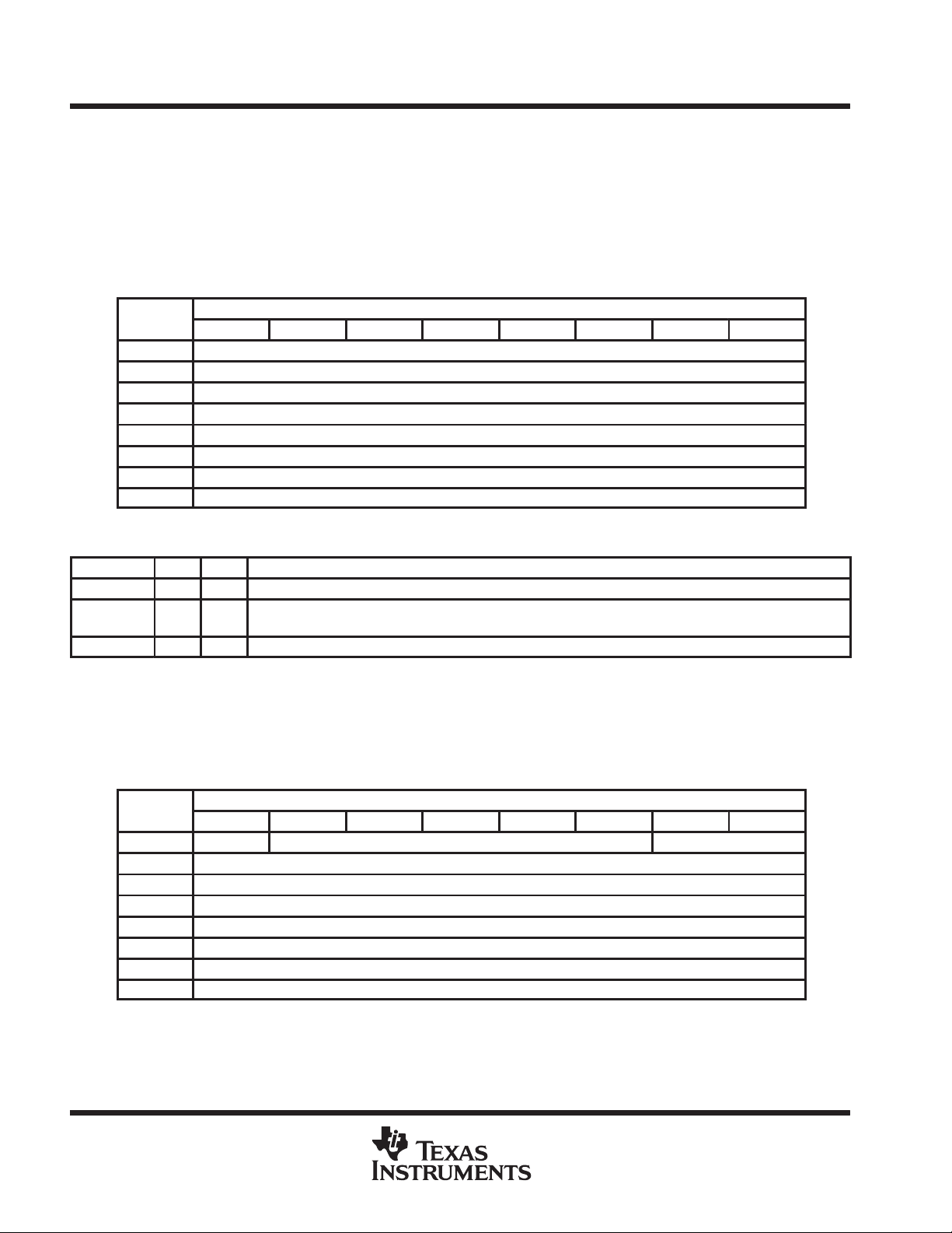
There are 16 accessible internal registers in the TSB41L V03A. The configuration of the registers at addresses
0h through 7h (the base registers) is fixed, while the configuration of the registers at addresses 8h through Fh
(the paged registers) is dependent upon which one of eight pages, numbered 0h through 7h, is currently
selected. The selected page is set in base register 7h.
The configuration of the base registers is shown in T able 1, and corresponding field descriptions given in T able 2
The base register field definitions are unaffected by the selected page number.
A reserved register or register field (marked as Reserved or Rsvd in the following register configuration tables)
is read as 0, but is subject to future usage. All registers in address pages 2 through 6 are reserved.
Table 1. Base Register Configuration
BIT POSITION
0 1 2 3 4 5 6 7
0000 Physical ID R CPS
0001 RHB IBR Gap_Count
0010 Extended (111b) Rsvd Num_Ports (0011b)
0011 PHY_Speed (010b) Rsvd Delay (0000b)
0100 LCtrl C Jitter (000b) Pwr_Class
0101 RPIE ISBR CTOI CPSI STOI PEI EAA EMC
0110 Reserved
0111 Page_Select Rsvd Port_Select
POST OFFICE BOX 655303 • DALLAS, TEXAS 75265
15

TSB41LV03A, TSB41LV03AI
IEEE 1394a THREE-PORT CABLE TRANSCEIVER/ARBITER
SLLS364A – JULY 1999 – REVISED MAY 2000
APPLICATION INFORMATION
internal register configuration (continued)
Table 2. Base Register Field Descriptions
FIELD SIZE TYPE DESCRIPTION
Physical ID 6 Rd This field contains the physical address ID of this node determined during self-ID. The physical-ID is invalid
after a bus reset until self-ID has completed as indicated by an unsolicited register-0 status transfer.
R 1 Rd Root. This bit indicates that this node is the root node. The R bit is reset to 0 by bus reset, and is set to 1 during
tree-ID if this node becomes root.
CPS 1 Rd Cable-power-status. This bit indicates the state of the CPS input terminal. The CPS terminal is normally tied
to serial bus cable power through a 400-kΩ resistor. A 0 in this bit indicates that the cable power voltage has
dropped below its threshold for ensured reliable operation.
RHB 1 Rd/Wr Root-holdoff bit. This bit instructs the PHY to attempt to become root after the next bus reset. The RHB bit is
reset to 0 by a hardware reset, and is unaffected by a bus reset.
IBR 1 Rd/Wr Initiate bus reset. This bit instructs the PHY to initiate a long (166 µs) bus reset at the next opportunity . Any
receive or transmit operation in progress when this bit is set will complete before the bus reset is initiated.
The IBR bit is reset to 0 after a hardware reset or a bus reset.
Gap_Count 6 Rd/Wr Arbitration gap count. This value is used to set the subaction (fair) gap, arb-reset gap, and arb-delay times.
The gap count can be set either by a write to the register, or by reception or transmission of a PHY_CONFIG
packet. The gap count is reset to 3Fh by hardware reset or after two consecutive bus resets without an
intervening write to the gap count register (either by a write to the PHY register or by a PHY_CONFIG
packet).
Extended 3 Rd Extended register definition. For the TSB41LV03A, this field is 1 11b, indicating that the extended register set
is implemented.
Num_Ports 4 Rd Number of ports. This field indicates the number of ports implemented in the PHY. For the TSB41LV03A this
field is 3.
PHY_Speed 3 Rd PHY speed capability. For the TSB41LV03A PHY this field is 010b, indicating S400 speed capability.
Delay 4 Rd PHY repeater data delay. This field indicates the worst case repeater data delay of the PHY, expressed as
144+(delay × 20) ns. For the TSB41LV03A this field is 0.
LCtrl 1 Rd/Wr Link-active status control. This bit is used to control the active status of the LLC as indicated during self-ID.
The logical AND of this bit and the LPS active status is replicated in the L field (bit 9) of the self-ID packet. The
LLC is considered active only if both the LPS input is active and the LCtrl bit is set.
The LCtrl bit provides a software controllable means to indicate the LLC active status in lieu of using the LPS
input.
The LCtrl bit is set to 1 by hardware reset and is unaffected by bus–reset.
NOTE: The state of the PHY-LLC interface is controlled solely by the LPS input, regardless of the state of the
LCtrl bit. If the PHY -LLC interface is operational as determined by the LPS input being active, then received
packets and status information will continue to be presented on the interface, and any requests indicated on
the LREQ input will be processed, even if the LCtrl bit is cleared to 0.
C 1 Rd/Wr Contender status. This bit indicates that this node is a contender for the bus or isochronous resource
manager. This bit is replicated in the c field (bit 20) of the self-ID packet. This bit is set to the state specified by
the C/LKON input terminal by a hardware reset and is unaffected by a bus reset.
Jitter 3 Rd PHY repeater jitter. This field indicates the worst case difference between the fastest and slowest repeater
data delay, expressed as (Jitter+1) × 20 ns. For the TSB41LV03A, this field is 0.
Pwr_Class 3 Rd/Wr Node power class. This field indicates this node power consumption and source characteristics and is
replicated in the pwr field (bits 21–23) of the self-ID packet. This field is reset to the state specified by the
PC0–PC2 input terminals upon a hardware reset, and is unaffected by a bus reset. See Table 9.
RPIE 1 Rd/Wr Resuming port interrupt enable. This bit, if set to 1, enables the port event interrupt (PIE) bit to be set
whenever resume operations begin on any port. This bit is reset to 0 by hardware reset and is unaffected by
bus reset.
16
POST OFFICE BOX 655303 • DALLAS, TEXAS 75265

TSB41LV03A, TSB41LV03AI
IEEE 1394a THREE-PORT CABLE TRANSCEIVER/ARBITER
SLLS364A – JULY 1999 – REVISED MAY 2000
APPLICATION INFORMATION
Table 2. Base Register Field Descriptions (Continued)
FIELD SIZE TYPE DESCRIPTION
ISBR 1 Rd/Wr Initiate short arbitrated bus reset. This bit, if set to 1, instructs the PHY to initiate a short (1.3 µs) arbitrated
CTOI 1 Rd/Wr Configuration time-out interrupt. This bit is set to 1 when the arbitration controller times-out during tree-ID
CPSI 1 Rd/Wr Cable power status interrupt. This bit is set to 1 whenever the CPS input transitions from high to low
STOI 1 Rd/Wr State-timeout interrupt. This bit indicates that a state time-out has occurred (which also causes a bus-reset
PEI 1 Rd/Wr Port event interrupt. This bit is set to 1 on any change in the connected, bias, disabled, or fault bits for any port
EAA 1 Rd/Wr Enable accelerated arbitration. This bit enables the PHY to perform the various arbitration acceleration
EMC 1 Rd/Wr Enable multispeed concatenated packets. This bit enables the PHY to transmit concatenated packets of
Page_Select 3 Rd/Wr Page_Select. This field selects the register page to use when accessing register addresses 8 through 15.
Port_Select 4 Rd/Wr Port_Select. This field selects the port when accessing per-port status or control (e.g., when one of the port
bus reset at the next opportunity. This bit is reset to 0 by a bus reset.
NOTE: Legacy IEEE Std 1394-1995 compliant PHYs can not be capable of performing short bus resets.
Therefore, initiation of a short bus reset in a network that contains such a legacy device results in a long bus
reset being performed.
start, and may indicate that the bus is configured in a loop. This bit is reset to 0 by hardware reset, or by
writing a 1 to this register bit.
If the CTOI and RPIE bits are both set and the LLC is or becomes inactive, the PHY will activate the C/LKON
output to notify the LLC to service the interrupt.
NOTE: If the network is configured in a loop, only those nodes which are part of the loop should generate a
configuration-timeout interrupt. All other nodes should instead time out waiting for the tree-ID and/or self-ID
process to complete and then generate a state time-out interrupt and bus-reset.
indicating that cable power may be too low for reliable operation. This bit is reset to 1 by hardware reset. It
can be cleared by writing a 1 to this register bit.
If the STOI and RPIE bits are both set and the LLC is or becomes inactive, the PHY will activate the C/LKON
output to notify the LLC to service the interrupt.
to occur). This bit is reset to 0 by hardware reset, or by writing a 1 to this register bit.
If the STOI and RPIE bits are both set and the LLC is or becomes inactive, the PHY will activate the C/LKON
output to notify the LLC to service the interrupt.
for which the port interrupt enable (PIE) bit is set. Additionally, if the resuming port interrupt enable (RPIE) bit
is set, the PEI bit is set to 1 at the start of resume operations on any port. This bit is reset to 0 by hardware
reset, or by writing a 1 to this register bit.
enhancements defined in P1394a (ACK-accelerated arbitration, asynchronous fly-by concatenation, and
isochronous fly-by concatenation). This bit is reset to 0 by hardware reset and is unaffected by bus reset.
NOTE: The EAA bit should be set only if the attached LLC is P1394a compliant. If the LLC is not P1394a
compliant, use of the arbitration acceleration enhancements can interfere with isochronous traffic by
excessively delaying the transmission of cycle-start packets.
differing speeds in accordance with the protocols defined in P1394a. This bit is reset to 0 by hardware reset
and is unaffected by bus reset.
NOTE: The use of multispeed concatenation is completely compatible with networks containing legacy
IEEE Std 1394-1995 PHYs. However, use of multispeed concatenation requires that the attached LLC be
P1394a compliant.
This field is reset to 0 by a hardware reset and is unaffected by bus-reset.
status/control registers is accessed in page 0). Ports are numbered starting at 0. This field is reset to 0 by
hardware-reset and is unaffected by bus-reset.
POST OFFICE BOX 655303 • DALLAS, TEXAS 75265
17

TSB41LV03A, TSB41LV03AI
IEEE 1394a THREE-PORT CABLE TRANSCEIVER/ARBITER
SLLS364A – JULY 1999 – REVISED MAY 2000
APPLICATION INFORMATION
internal register configuration (continued)
The port status page provides access to configuration and status information for each of the ports. The port is
selected by writing 0 to the Page_Select field and the desired port number to the Port_Select field in base
register 7. The configuration of the port status page registers is shown in Table 3 and corresponding field
descriptions given in T able 4. If the selected port is unimplemented, all registers in the port status page are read
as 0.
Table 3. Page 0 (Port Status) Register Configuration
BIT POSITION
Address 0 1 2 3 4 5 6 7
1000 AStat BStat Ch Con Bias Dis
1001 Peer_Speed PIE Fault Reserved
1010 Reserved
1011 Reserved
1100 Reserved
1101 Reserved
1110 Reserved
1111 Reserved
18
POST OFFICE BOX 655303 • DALLAS, TEXAS 75265

TSB41LV03A, TSB41LV03AI
IEEE 1394a THREE-PORT CABLE TRANSCEIVER/ARBITER
SLLS364A – JULY 1999 – REVISED MAY 2000
APPLICATION INFORMATION
internal register configuration (continued)
Table 4. Page 0 (Port Status) Register Field Descriptions
FIELD SIZE TYPE DESCRIPTION
AStat 2 Rd TPA line state. This field indicates the TPA line state of the selected port, encoded as follows:
BStat 2 Rd TPB line state. This field indicates the TPB line state of the selected port. This field has the same encoding as
the ASTAT field.
Ch 1 Rd Child/parent status. A 1 indicates that the selected port is a child port. A 0 indicates that the selected port is the
parent port. A disconnected, disabled, or suspended port is reported as a child port. The Ch bit is invalid after a
bus-reset until tree-ID has completed.
Con 1 Rd Debounced port connection status. This bit indicates that the selected port is connected. The connection must
be stable for the debounce time of approximately 341 ms for the Con bit to be set to 1. The Con bit is reset to 0 by
hardware reset and is unaffected by bus reset.
NOTE: The Con bit indicates that the port is physically connected to a peer PHY , but the port is not necessarily
active.
Bias 1 Rd Debounced incoming cable bias status. A 1 indicates that the selected port is detecting incoming cable bias.
The incoming cable bias must be stable for the debounce time of 52 µs for the Bias bit to be set to 1.
Dis 1 Rd/Wr Port disabled control. If 1, the selected port is disabled. The Dis bit is reset to 0 by hardware reset (all ports are
enabled for normal operation following hardware reset). The Dis bit is not affected by bus reset.
Peer_Speed 3 Rd Port peer speed. This field indicates the highest speed capability of the peer PHY connected to the selected
port, encoded as follows:
The Peer_Speed field is invalid after a bus reset until self-ID has completed.
NOTE: Peer speed codes higher than 010b (S400) are defined in P1394a. However, the TSB41L V03A is only
capable of detecting peer speeds up to S400.
PIE 1 Rd/Wr Port event interrupt enable. When set to 1, a port event on the selected port will set the port event interrupt (PEI)
bit and notify the link. This bit is reset to 0 by a hardware reset, and is unaffected by bus-reset.
Fault 1 Rd/Wr Fault. This bit indicates that a resume-fault or suspend-fault has occurred on the selected port, and that the port
is in the suspended state. A resume-fault occurs when a resuming port fails to detect incoming cable bias from
its attached peer. A suspend-fault occurs when a suspending port continues to detect incoming cable bias from
its attached peer. Writing 1 to this bit clears the fault bit to 0. This bit is reset to 0 by hardware reset and is
unaffected by bus reset.
Code Arb Value
11 Z
01 1
10 0
00 invalid
Code Peer Speed
000 S100
001 S200
010 S400
011–111 invalid
POST OFFICE BOX 655303 • DALLAS, TEXAS 75265
19
TSB41LV03A, TSB41LV03AI
IEEE 1394a THREE-PORT CABLE TRANSCEIVER/ARBITER
SLLS364A – JULY 1999 – REVISED MAY 2000
APPLICATION INFORMATION
internal register configuration (continued)
The Vendor Identification page is used to identify the vendor/manufacturer and compliance level. The page is
selected by writing 1 to the Page_Select field in base register 7. The configuration of the Vendor Identification
page is shown in Table 5, and corresponding field descriptions given in Table 6.
Table 5. Page 1 (Vendor ID) Register Configuration
BIT POSITION
Address 0 1 2 3 4 5 6 7
1000 Compliance
1001 Reserved
1010 Vendor_ID[0]
1011 Vendor_ID[1]
1100 Vendor_ID[2]
1101 Product_ID[0]
1110 Product_ID[1]
1111 Product_ID[2]
Table 6. Page 1 (Vendor ID) Register Field Descriptions
FIELD SIZE TYPE DESCRIPTION
Compliance 8 Rd Compliance level. For the TSB41L V03A this field is 01h, indicating compliance with the P1394a specification.
Vendor_ID 24 Rd Manufacturer’s organizationally unique identifier (OUI). For the TSB41LV03A this field is 08_00_28h (Texas
Product_ID 24 Rd Product identifier. For the TSB41LV03A this field is 00_00_00h (the MSB is at register address 1101b).
Instruments) (the MSB is at register address 1010b).
The Vendor-Dependent page provides access to the special control features of the TSB41LV03A, as well as
configuration and status information used in manufacturing test and debug. This page is selected by writing 7
to the Page_Select field
in base register 7. The configuration of the Vendor-Dependent page is shown in T able 7
and corresponding field descriptions given in Table 8.
Table 7. Page 7 (Vendor-Dependent) Register Configuration
BIT POSITION
Address 0 1 2 3 4 5 6 7
1000 NPA Reserved Link_Speed
1001 Reserved for test
1010 Reserved for test
1011 Reserved for test
1100 Reserved for test
1101 Reserved for test
1110 Reserved for test
1111 Reserved for test
20
POST OFFICE BOX 655303 • DALLAS, TEXAS 75265

TSB41LV03A, TSB41LV03AI
IEEE 1394a THREE-PORT CABLE TRANSCEIVER/ARBITER
SLLS364A – JULY 1999 – REVISED MAY 2000
APPLICATION INFORMATION
internal register configuration (continued)
Table 8. Page 7 (Vendor-Dependent) Register Field Descriptions
FIELD SIZE TYPE DESCRIPTION
NPA 1 Rd/Wr Null-packet actions flag. This bit instructs the PHY to not clear fair and priority requests when a null packet is
Link_Speed 2 Rd/Wr Link speed. This field indicates the top speed capability of the attached LLC. Encoding is as follows:
received with arbitration acceleration enabled. If 1, then fair and priority requests are cleared only when a
packet of more than 8 bits is received; ACK packets (exactly 8 data bits), null packets (no data bits), and
mal-formed packets (less than 8 data bits) will not clear fair and priority requests. If 0, then fair and priority
requests are cleared when any non-ACK packet is received, including null-packets or mal-formed packets of
less than 8 bits. This bit is cleared to 0 by hardware reset and is unaffected by bus-reset.
Code Speed
00 S100
01 S200
10 S400
11 illegal
This field is replicated in the sp field of the self-ID packet to indicate the speed capability of the node (PHY
and LLC in combination). However, this field does not affect the PHY speed capability indicated to peer
PHYs during self-ID; the TSB41LV03A PHY identifies itself as S400 capable to its peers regardless of the
value in this field. This field is set to 10b (S400) by hardware reset and is unaffected by bus-reset.
power-class programming
The PC0–PC2 terminals are programmed to set the default value of the power-class indicated in the pwr field
(bits 21–23) of the transmitted self-ID packet. Descriptions of the various power-classes are given in Table 9
The default power-class value is loaded following a hardware reset, but is overriden by any value subsequently
loaded into the Pwr_Class field in register 4.
Table 9. Power Class Descriptions
PC0–PC2 DESCRIPTION
000 Node does not need power and does not repeat power.
001 Node is self-powered and provides a minimum of 15 W to the bus.
010 Node is self-powered and provides a minimum of 30 W to the bus.
011 Node is self-powered and provides a minimum of 45 W to the bus.
100 Node may be powered from the bus and is using up to 3 W and may also provide power to the bus. The amount of bus
101 Node is powered from the bus and uses up to 3 W. No additional power is needed to enable the link and higher layers of
110 Node is powered from the bus and uses up to 3 W. An additional 3 W is needed to enable the link.
111 Node is powered from the bus and uses up to 3 W. An additional 7 W is needed to enable the link.
power that it provides can be found in the configuration ROM.
the node.
POST OFFICE BOX 655303 • DALLAS, TEXAS 75265
21

TSB41LV03A, TSB41LV03AI
IEEE 1394a THREE-PORT CABLE TRANSCEIVER/ARBITER
SLLS364A – JULY 1999 – REVISED MAY 2000
APPLICATION INFORMATION
Outer Shield
Termination
TSB41LV03A
CPS
TPBIAS
TPA+
TPA–
Cable Port
TPB+
TPB–
NOTE A: The IEEE Std 1394-1995 calls for a 250-pF capacitor, which is a nonstandard component value. A 220-pF capacitor is recommended.
400 kΩ
220 pF
(see Note A)
56 Ω56 Ω
1 µF
Cable
Power
Pair
Cable
Pair
A
Cable
Pair
B
56 Ω56 Ω
5 kΩ
22
Figure 4. TP Cable Connections
Outer Cable Shield
1 MΩ
Chassis Ground
0.001 µF0.01 µF
Figure 5. Typical Compliant DC Isolated Outer Shield Termination
POST OFFICE BOX 655303 • DALLAS, TEXAS 75265

TSB41LV03A, TSB41LV03AI
IEEE 1394a THREE-PORT CABLE TRANSCEIVER/ARBITER
SLLS364A – JULY 1999 – REVISED MAY 2000
APPLICATION INFORMATION
Outer Cable Shield
Chassis Ground
Figure 6. Non-DC Isolated Outer Shield Termination
10 kΩ
Link Power
LPS
Square Wave Input
Figure 7. Non-Isolated Connection Variations for LPS
Square Wave Signal
Figure 8. Isolated Circuit Connection for LPS
0.033 µF
10 kΩ
13 kΩ
PHY GND
PHY V
LPS
DD
18 kΩ
LPS
POST OFFICE BOX 655303 • DALLAS, TEXAS 75265
23

TSB41LV03A, TSB41LV03AI
IEEE 1394a THREE-PORT CABLE TRANSCEIVER/ARBITER
SLLS364A – JULY 1999 – REVISED MAY 2000
APPLICATION INFORMATION
V
DD
0.1 µF
V
DD
Link V
DD
CNA Out
Power Down
Link Pulse
or V
0.1 µF
DD
V
C9
(see
Note A)
0.1 µF
0.001 µF
1
LREQ
2
SYSCLK
3
DGND
4
CTL0
5
CTL1
0.001 µF
6
DV
DD
7
D0
8
D1
9
V
DD-5V
10
D2
11
D3
12
0.1 µF
DD
13
14
15
16
17
18
19
20
D4
D5
D6
D7
DGND
CNA
PD
LPS
DGND
C10
(see
Note A)
0.1 µF
24.576 MHz
79 78 77 76 7580 74
XI
XO
DD
DV
DGND
RESET
0.001 µF 0.1 µF
72 71 7073
PLLGND
PLLGND
0.001 µF
0.001 µF
0.1 µF
DD
PLLV
FILTER0
FILTER1
TSB41LV03A
DD
DGND
C/LKON
PC0
21 22 23 24 25 26 27 28
PC1
PC2
ISO
DGND
CPS
29 30 31 32 33
DV
DVDDTESTMSESM
DD
V
6.34 kΩ
±1%
69 68 67 66 65
DD
R1
DD
DV
DV
DGND
AVDDAVDDAGND
34 35 36
64 63 62 61
R0
AGND
AGND
AGND
37 38 39 40
1 MΩ
±0.5%
DD
AVDDAV
AGND
TPBIAS2
TPA2+
TPA2–
TPB2+
TPB2–
AV
TPBIAS1
TPA1+
TPA1–
TPB1+
TPB1–
AV
AV
TPBIAS0
TPA0+
TPA0–
TPB0+
TPB0–
AGND
AGND
AGND
AGND
DD
DD
DD
AGND
0.1 µF
60
58
57
56
55
54
53
52
51
50
49
48
47
46
45
44
43
42
41
0.001 µF
59
DD
V
0.001 µF
0.001 µF
0.1 µF
1 µF
TPBIAS
TP Cables
Interface
Connection
V
DD
TPBIAS
1 µF
TP Cables
Interface
Connection
V
DD
TPBIAS
1 µF
TP Cables
Interface
Connection
0.001 µF
0.001 µF
10 kΩ
LKON
Bus
Manager
NOTE A: See Crystal Selection section
24
V
0.001 µF
0.001 µF
0.1 µF
DD
ISO
Power-Class
Programming
400 kΩ
Cable Power
0.001 µF
0.1 µF
DD
1 kΩ
V
0.001 µF
Figure 9. External Component Connections
POST OFFICE BOX 655303 • DALLAS, TEXAS 75265
0.01 µF

TSB41LV03A, TSB41LV03AI
IEEE 1394a THREE-PORT CABLE TRANSCEIVER/ARBITER
SLLS364A – JULY 1999 – REVISED MAY 2000
APPLICATION INFORMATION
designing with PowerPAD
The TSB41LV03A is housed in a high performance, thermally enhanced, 80-pin PFP PowerPAD package.
Use of the PowerPAD package does not require any special considerations except to note that the
PowerPAD, which is an exposed die pad on the bottom of the device, is a metallic thermal and electrical
conductor. Therefore, if not implementing PowerPAD PCB features, the use of solder masks (or other
assembly techniques) may be required to prevent any inadvertent shorting by the exposed PowerPAD of
connection etches or vias under the package. The recommended option, however, is to not run any etches or
signal vias under the device, but to have only a grounded thermal land as explained below. Although the actual
size of the exposed die pad may vary, the minimum size required for the keepout area for the 80-pin PFP
PowerPAD package is 10 mm × 10 mm.
It is recommended that there be a thermal land, which is an area of solder-tinned-copper, underneath the
PowerPAD package. The thermal land will vary in size, depending on the PowerPAD package being used,
the PCB construction, and the amount of heat that needs to be removed. In addition, the thermal land may or
may not contain numerous thermal vias depending on PCB construction.
Other requirements for thermal lands and thermal vias are detailed in the TI application note
Thermally Enhanced Package Application Report
pages beginning at URL: http://www.ti.com.
, TI literature number SLMA002, available via the TI Web
PowerPAD
Figure 10. Example of a Thermal Land for the TSB41LV03A PHY
For the TSB41L V03A, this thermal land should be grounded to the low impedance ground plane of the device.
This improves not only thermal performance but also the electrical grounding of the device. It is also
recommended that the device ground terminal landing pads be connected directly to the grounded thermal land.
The land size should be as large as possible without shorting device signal terminals. The thermal land may
be soldered to the exposed PowerPAD using standard reflow soldering techniques.
While the thermal land may be electrically floated and configured to remove heat to an external heat sink, it is
recommended that the thermal land be connected to the low impedance ground plane for the device. More
information may be obtained from the TI application note
PHY Layout
, TI literature number SLLA020.
using the TSB41LV03A with a non-P1394a link layer
The TSB41LV03A implements the PHY-LLC interface specified in the P1394a Supplement. This interface is
based upon the interface described in informative Annex J of IEEE Std 1394-1995, which is the interface used
in older TI PHY devices. The PHY-LLC interface specified in P1394a is completely compatible with the older
Annex J interface.
POST OFFICE BOX 655303 • DALLAS, TEXAS 75265
25

TSB41LV03A, TSB41LV03AI
IEEE 1394a THREE-PORT CABLE TRANSCEIVER/ARBITER
SLLS364A – JULY 1999 – REVISED MAY 2000
APPLICATION INFORMATION
using the TSB41LV03A with a non-P1394a link layer (continued)
The P1394a Supplement includes enhancements to the Annex J interface that must be comprehended when
using the TSB41LV03A with a non-P1394a LLC device.
D
A new LLC service request was added which allows the LLC to temporarily enable and disable
asynchronous arbitration accelerations. If the LLC does not implement this new service request, the
arbitration enhancements should not be enabled (see the EAA bit in PHY register 5).
D
The capability to perform multispeed concatenation (the concatenation of packets of differing speeds) was
added in order to improve bus efficiency (primarily during isochronous transmission). If the LLC does not
support multispeed concatenation, multispeed concatenation should not be enabled in the PHY (see the
EMC bit in PHY register 5).
D
In order to accommodate the higher transmission speeds expected in future revisions of the standard,
P1394A extended the speed code in bus requests from 2 bits to 3 bits, increasing the length of the bus
request from 7 bits to 8 bits. The new speed codes were carefully selected so that new P1394a PHY and
LLC devices would be compatible, for speeds from S100 to S400, with legacy PHY and LLC devices that
use the 2-bit speed codes. The TSB41L V03A correctly interprets both 7-bit bus requests (with 2-bit speed
code) and 8-bit bus requests (with 3-bit speed codes). Moreover, if a 7-bit bus request is immediately
followed by another request (e.g., a register read or write request), the TSB41LV03A correctly interprets
both requests. Although the TSB41LV03A correctly interprets 8-bit bus requests, a request with a speed
code exceeding S400 results in the TSB41LV03A transmitting a null packet (data-prefix followed by
data-end, with no data in the packet).
More explanation is included in the TI application note
Physical Layer Devices,
TI literature number SLL019.
IEEE 1394a Features Supported by TI TSB41LV0X
using the TSB41LV03A with a lower-speed link layer
Although the TSB41L V03A is an S400-capable PHY, it may be used with lower speed LLCs, such as the S200
capable TSB12L V31. In such a case, the LLC has fewer data terminals than the PHY, and some Dn terminals
on the TSB41L V03A will be unused. Unused Dn terminals should be pulled to ground through 10-kΩ resistors.
The TSB41LV03A transfers all received packet data to the LLC, even if the speed of the packet exceeds the
capability of the LLC to accept it. Some lower speed LLC designs do not properly ignore packet data in such
cases. On the rare occasions that the first 16 bits of partial data accepted by such a LLC match a node’s bus
and node ID, spurious header CRC or tcode errors may result.
During bus initialization following a bus-reset, each PHY transmits a self-ID packet that indicates, among other
information, the speed capability of the PHY. The bus manager (if one exists) builds a speed-map from the
collected self-ID packets. This speed-map gives the highest possible speed that can be used on the
node-to-node communication path between every pair of nodes in the network.
In the case of a node consisting of a higher-speed PHY and a lower-speed LLC, the speed capability of the node
(PHY and LLC in combination) is that of the lower-speed LLC. A sophisticated bus manager may be able to
determine the LLC speed capability by reading the configuration ROM Bus_Info_Block, or by sending
asynchronous request packets at different speeds to the node and checking for an acknowledge; the
speed-map may then be adjusted accordingly. The speed-map should reflect that communication to such a
node must be done at the lower speed of the LLC, instead of the higher speed of the PHY . However , speed-map
entries for paths that merely pass through the node’s PHY, but do not terminate at that node, should not be
restricted by the lower speed of the LLC.
26
POST OFFICE BOX 655303 • DALLAS, TEXAS 75265

TSB41LV03A, TSB41LV03AI
IEEE 1394a THREE-PORT CABLE TRANSCEIVER/ARBITER
SLLS364A – JULY 1999 – REVISED MAY 2000
APPLICATION INFORMATION
using the TSB41LV03A with a lower-speed link layer (continued)
To assist in building an accurate speed-map, the TSB41LV03A has the capability of indicating a speed other
than S400 in its transmitted self-ID packet. This is controlled by the Link_Speed field in register 8 of the
Vendor-Dependent page (page 7). Setting the Link_Speed field af fects only the speed indicated in the self-ID
packet; it has no effect on the speed signaled to peer PHYs during self-ID. The TSB41LV03A identifies itself
as S400 capable to its peers regardless of the value in the Link_Speed field.
Generally, the Link_Speed field should not be changed from its power-on default value of S400 unless it is
determined that the speed-map (if one exists) is incorrect for path entries terminating in the local node. If the
speed-map is incorrect, it can be assumed that the bus manager has used only the self-ID packet information
to build the speed-map. In this case, the node may update the Link_Speed field to reflect the lower speed
capability of the LLC and then initiate another bus-reset to cause the speed-map to be rebuilt. Note that in this
scenario any speed-map entries for node-to-node communication paths that pass through the local node’s PHY
will be restricted by the lower speed.
In the case of a leaf node (which has only one active port) the Link_Speed field may be set to indicate the speed
of the LLC without first checking the speed-map. Changing the Link_Speed field in a leaf node can only affect
those paths that terminate at that node, since no other paths can pass through a leaf node. It can have no effect
on other paths in the speed-map. For hardware configurations which can only be a leaf node (all ports but one
are unimplemented), it is recommended that the Link_Speed field be updated immediately after power-on or
hardware reset.
power-up reset
To ensure proper operation of the TSB41LV03A the RESET
2 ms from the time that PHY power reaches the minimum required supply voltage. When using a passive
capacitor on the RESET
if the value of the capacitor has a minimum value of 0.1 µF and also satisfies the following equation:
C
= 0.0077 × T + 0.085
min
where C
in ms.
is the minimum capacitance on the RESET terminal in µF , and T is the VDD ramp time, 10%–90%,
min
terminal to generate a power-on reset signal, the minimum reset time will be assured
terminal must be asserted low for a minimum of
crystal selection
The TSB41LV03A and other TI PHY devices are designed to use an external 24.576 MHz crystal connected
between the XI and XO terminals to provide the reference for an internal oscillator circuit. This oscillator in turn
drives a PLL circuit that generates the various clocks required for transmission and resynchronization of data
at the S100 through S400 media data rates.
A variation of less than ±100 ppm from nominal for the media data rates is required by IEEE Std 1394. Adjacent
PHYs may therefore have a difference of up to 200 ppm from each other in their internal clocks, and PHYs must
be able to compensate for this difference over the maximum packet length. Larger clock variations may cause
resynchronization overflows or underflows, resulting in corrupted packet data.
For the TSB41L V03A, the SYSCLK output may be used to measure the frequency accuracy and stability of the
internal oscillator and PLL from which it is derived. The frequency of the SYSCLK output must be within ±100
ppm of the nominal frequency of 49.152 MHz.
POST OFFICE BOX 655303 • DALLAS, TEXAS 75265
27

TSB41LV03A, TSB41LV03AI
IEEE 1394a THREE-PORT CABLE TRANSCEIVER/ARBITER
SLLS364A – JULY 1999 – REVISED MAY 2000
APPLICATION INFORMATION
crystal selection (continued)
The following are some typical specifications for crystals used with the physical layers from TI in order to achieve
the required frequency accuracy and stability:
D
Crystal mode of operation: Fundamental
D
Frequency tolerance at 25°C: Total frequency variation for the complete circuit is ±100 ppm. A crystal with
±30 ppm frequency tolerance is recommended for adequate margin.
D
Frequency stability (over temperature and age): A crystal with ±30 ppm frequency stability is recommended
for adequate margin.
NOTE:
The total frequency variation must be kept below ±100 ppm from nominal with some allowance for
error introduced by board and device variations. Trade-offs between frequency tolerance and
stability may be made as long as the total frequency variation is less than ±100 ppm. For example,
the frequency tolerance of the crystal may be specified at 50 ppm and the temperature tolerance
may be specified at 30 ppm to give a total of 80 ppm possible variation due to the crystal alone.
Crystal aging also contributes to the frequency variation.
D
Load capacitance: For parallel resonant mode crystal circuits, the frequency of oscillation is dependent
upon the load capacitance specified for the crystal. T otal load capacitance (CL) is a function of not only the
discrete load capacitors, but also board layout and circuit. It may be necessary to iteratively select discrete
load capacitors until the SYSCLK output is within specification. It is recommended that load capacitors with
a maximum of ±5% tolerance be used.
As an example, for the OHCI + 41LV03 evaluation module (EVM) which uses a crystal specified for 12 pF
loading, load capacitors (C9 and C10 in Figure 1 1) of 16 pF each were appropriate for the layout of that particular
board. The load specified for the crystal includes the load capacitors (C9, C10), the loading of the PHY terminals
(C
), and the loading of the board itself (CBD). The value of C
PHY
is typically about 1 pF , and CBD is typically
PHY
0.8 pF per centimeter of board etch; a typical board can have 3 pF to 6 pF or more. The load capacitors C9 and
C10 combine as capacitors in series so that the total load capacitance is:
CL = [(C9 × C10) / (C9+C10)] + C
+ CBD.
PHY
C9
24.576 MHz
Is
C10
X1
C
PHY
+ C
XI
BD
XO
Figure 11. Load Capacitance for the TSB41LV03A PHY
NOTE:
The layout of the crystal portion of the PHY circuit is important for obtaining the correct frequency ,
minimizing noise introduced into the PHY’s Phase Lock Loop, and minimizing any emissions from
the circuit. The crystal and two load capacitors should be considered as a unit during layout. The
crystal and load capacitors should be placed as close as possible to one another while minimizing
the loop area created by the combination of the three components. V arying the size of the capacitors
may help in this. Minimizing the loop area minimizes the effect of the resonant current (Is) that flows
in this resonant circuit. This layout unit (crystal and load capacitors) should then be placed as close
as possible to the PHY XI and XO terminals to minimize trace lengths.
28
POST OFFICE BOX 655303 • DALLAS, TEXAS 75265

TSB41LV03A, TSB41LV03AI
IEEE 1394a THREE-PORT CABLE TRANSCEIVER/ARBITER
SLLS364A – JULY 1999 – REVISED MAY 2000
APPLICATION INFORMATION
crystal selection (continued)
C9
C10
X1
Figure 12. Recommended Crystal and Capacitor Layout
It is strongly recommended that part of the verification process for the design be to measure the frequency of
the SYSCLK output of the PHY. This should be done with a frequency counter with an accuracy of 6 digits or
better. If the SYSCLK frequency is more than the crystal’s tolerance from 49.152 MHz, the load capacitance
of the crystal may be varied to improve frequency accuracy. If the frequency is too high, add more load
capacitance; if the frequency is too low, decrease load capacitance. T ypically, changes should be done to both
load capacitors (C9 and C10 above) at the same time, and both should be of the same value. Additional design
details and requirements may be provided by the crystal vendor.
bus reset
In the TSB41L V03A, the initiate bus reset (IBR) bit may be set to 1 in order to initiate a bus reset and initialization
sequence. The IBR bit is located in PHY register 1, along with the root-holdoff (RHB) bit and gap-count register ,
as required by the P1394a Supplement (this configuration also maintains compatibility with older TI PHY
designs which were based upon the suggested register set defined in Annex J of IEEE Std 1394-1995).
Therefore, whenever the IBR bit is written, the RHB bit and gap-count are also necessarily written.
The RHB bit and gap-count may also be updated by PHY-config packets. The TSB41LV03A is P1394a
compliant, and therefore both the reception and transmission of PHY-config packets cause the RHB and
gap-count to be loaded, unlike older IEEE Std 1394-1995 compliant PHYs which decode only received
PHY-config packets.
The gap-count will be set to the maximum value of 63 after two consecutive bus resets without an intervening
write to the gap-count, either by a write to PHY register 1 or by a PHY-config packet. This mechanism allows
a PHY -config packet to be transmitted and then a bus reset initiated so as to verify that all nodes on the bus have
updated their RHB bits and gap-count values, without having the gap-count set back to 63 by the bus reset. The
subsequent connection of a new node to the bus, which initiates a bus reset, will then cause the gap-count of
each node to be set to 63. Note, however, that if a subsequent bus reset is instead initiated by a write to register
1 to set the IBR bit, all other nodes on the bus will have their gap-count values set to 63, while this node’s
gap-count remains set to the value just loaded by the write to PHY register 1.
Therefore, in order to maintain consistent gap-counts throughout the bus, the following rules apply to the use
of the IBR bit, RHB bit, and gap-count in PHY register 1:
D
Following the transmission of a PHY-config packet, a bus reset must be initiated in order to verify that all
nodes have correctly updated their RHB bits and gap-count values, and to ensure that a subsequent new
connection to the bus will cause the gap-count to be set to 63 on all nodes in the bus. If this bus reset is
initiated by setting the IBR bit to 1, the RHB bit and gap-count register must also be loaded with the correct
values consistent with the just transmitted PHY-config packet. In the TSB41LV03A, the RHB bit and
gap-count will have been updated to their correct values upon the transmission of the PHY -config packet,
and so these values may first be read from register 1 and then rewritten.
D
Other than to initiate the bus reset which must follow the transmission of a PHY-config packet, whenever
the IBR bit is set to 1 in order to initiate a bus reset, the gap-count value must also be set to 63 so as to be
consistent with other nodes on the bus, and the RHB bit should be maintained with its current value.
D
The PHY register 1 should not be written to except to set the IBR bit. The RHB bit and gap-count should
not be written without also setting the IBR bit to 1.
POST OFFICE BOX 655303 • DALLAS, TEXAS 75265
29

TSB41LV03A, TSB41LV03AI
IEEE 1394a THREE-PORT CABLE TRANSCEIVER/ARBITER
SLLS364A – JULY 1999 – REVISED MAY 2000
PRINCIPLES OF OPERATION
The TSB41L V03A is designed to operate with an LLC such as the T exas Instruments TSB12L V21, TSB12LV22,
TSB12LV23, TSB12LV31, TSB12LV41, TSB12LV42, or TSB12LV01A. Details of operation for the Texas
Instruments LLC devices are found in the respective LLC data sheets. The following paragraphs describe the
operation of the PHY-LLC interface.
The interface to the LLC consists of the SYSCLK, CTL0–CTL1, D0–D7, LREQ, LPS, C/LKON, and ISO
terminals on the TSB41LV03A, as shown in Figure 13.
TSB41LV03A
SYSCLK
CTL0–CTL1
LINK
LAYER
CONTROLLER
D0–D7
LREQ
LPS
C/LKON
ISO
ISO
ISO
Figure 13. PHY-LLC Interface
The SYSCLK terminal provides a 49.152-MHz interface clock. All control and data signals are synchronized to,
and sampled on, the rising edge of SYSCLK.
The CTL0 and CTL1 terminals form a bidirectional control bus, which controls the flow of information and data
between the TSB41LV03A and LLC.
The D0–D7 terminals form a bidirectional data bus, which is used to transfer status information, control
information, or packet data between the devices. The TSB41LV03A supports S100, S200, and S400 data
transfers over the D0–D7 data bus. In S100 operation only the D0 and D1 terminals are used; in S200 operation
only the D0–D3 terminals are used; and in S400 operation all D0–D7 terminals are used for data transfer. When
the TSB41LV03A is in control of the D0–D7 bus, unused Dn terminals are driven low during S100 and S200
operations. When the LLC is in control of the D0–D7 bus, unused Dn terminals are ignored by the TSB41L V03A.
The LREQ terminal is controlled by the LLC to send serial service requests to the PHY in order to request access
to the serial-bus for packet transmission, read or write PHY registers, or control arbitration acceleration.
The LPS and C/LKON terminals are used for power management of the PHY and LLC. The LPS terminal
indicates the power status of the LLC, and may be used to reset the PHY -LLC interface or to disable SYSCLK.
The C/LKON terminal is used to send a wake-up notification to the LLC and to indicate an interrupt to the LLC
when either LPS is inactive or the PHY register L bit is zero.
The ISO terminal is used to enable the output differentiation logic on the CTL0–CTL1 and D0–D7 terminals.
Output differentiation is required when an isolation barrier of the type described in Annex J type isolation barrier
is implemented between the PHY and LLC.
The TSB41LV03A normally controls the CTL0–CTL1 and D0–D7 bidirectional buses. The LLC is allowed to
drive these buses only after the LLC has been granted permission to do so by the PHY.
30
POST OFFICE BOX 655303 • DALLAS, TEXAS 75265
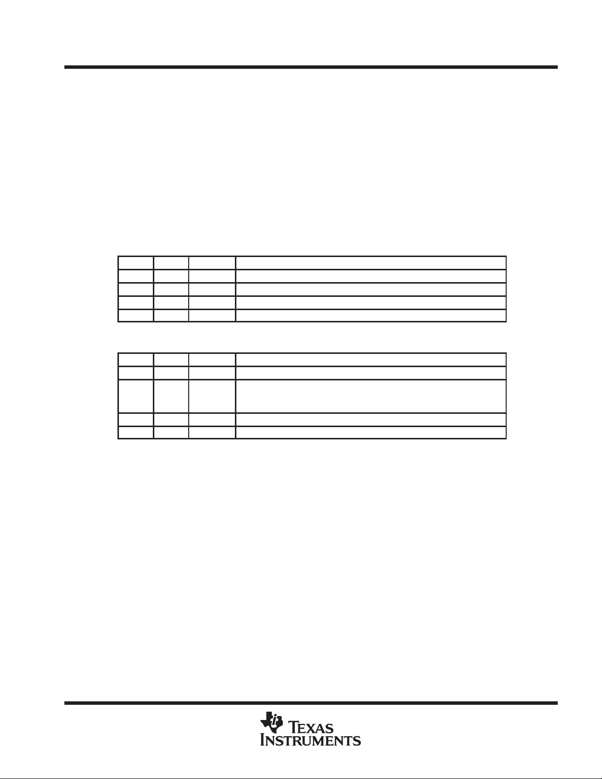
TSB41LV03A, TSB41LV03AI
IEEE 1394a THREE-PORT CABLE TRANSCEIVER/ARBITER
SLLS364A – JULY 1999 – REVISED MAY 2000
PRINCIPLES OF OPERATION
There are four operations that may occur on the PHY -LLC interface: link service request, status transfer, data
transmit, and data receive. The LLC issues a service request to read or write a PHY register, to request the PHY
to gain control of the serial-bus in order to transmit a packet, or to control arbitration acceleration.
The PHY may initiate a status transfer either autonomously or in response to a register read request from the
LLC.
The PHY initiates a receive operation whenever a packet is received from the serial-bus.
The PHY initiates a transmit operation after winning control of the serial-bus following a bus-request by the LLC.
The transmit operation is initiated when the PHY grants control of the interface to the LLC.
The encoding of the CTL0-CTL1 bus is shown in Table 10 and Table 11.
Table 10. CTL Encoding When PHY Has Control of the Bus
CTL0 CTL1 NAME DESCRIPTION
0 0 Idle No activity (this is the default mode)
0 1 Status Status information is being sent from the PHY to the LLC.
1 0 Receive An incoming packet is being sent from the PHY to the LLC.
1 1 Grant The LLC has been given control of the bus to send an outgoing packet.
Table 11. CTL Encoding When LLC Has Control of the Bus
CTL0 CTL1 NAME DESCRIPTION
0 0 Idle The LLC releases the bus (transmission has been completed)
0 1 Hold The LLC is holding the bus while data is being prepared for transmission, or
1 0 Transmit An outgoing packet is being sent from the LLC to the PHY
1 1 Reserved None
indicating that another packet is to be transmitted (concatenated) without
arbitrating
output differentiation
When an Annex J type isolation barrier is implemented between the PHY and LLC, the CTL0–CTL1, D0–D7,
and LREQ signals must be digitally differentiated so that the isolation circuits function correctly. Digital
differentiation is enabled on the TSB41LV03A when the /ISO terminal is low.
The differentiation operates such that the output is driven either low or high for one clock period whenever the
signal changes logic state, but otherwise places the output in a high–impedance state for as long as the signal
logic state remains constant. On input, hysteresis buffers are used to convert the signal to the correct logic state
when the signal is high–impedance; the biasing network of the Annex J type isolation circuit pulls the signal
voltage level between the hysteresis thresholds of the input buffer so that the previous logic state is maintained.
The correspondence between output logic state and output signal level is illustrated in Figure 14.
POST OFFICE BOX 655303 • DALLAS, TEXAS 75265
31

TSB41LV03A, TSB41LV03AI
IEEE 1394a THREE-PORT CABLE TRANSCEIVER/ARBITER
SLLS364A – JULY 1999 – REVISED MAY 2000
PRINCIPLES OF OPERATION
output differentiation (continued)
Logic State
011000 010
Signal Level
LHZ0ZZ LHZ
Figure 14. Signal Transformation for Digital Differentiation
Input Buffer
With
Hysteresis
DIn
DOut
To/From
Internal
Device
Logic
ISO
OutEn
Init
SysClk
DQ
QD
3-State
Output
Driver
QD
Figure 15. Signal Transformation for Digital Differentiation
The TSB41L V03A implements differentiation circuitry functionally equivalent to that shown in Figure 15 on the
bidirectional CTL0–CTL1and D0–D7 terminals. The TSB41L V03A also implements an input hysteresis buffer
on the LREQ input to convert this signal to the correct logic level when differentiated. The LLC must also
implement similar output differentiation and input hysteresis circuitry on its CTL and D terminals, and output
differentiation circuitry on its LREQ terminal.
D
32
POST OFFICE BOX 655303 • DALLAS, TEXAS 75265

TSB41LV03A, TSB41LV03AI
IEEE 1394a THREE-PORT CABLE TRANSCEIVER/ARBITER
SLLS364A – JULY 1999 – REVISED MAY 2000
PRINCIPLES OF OPERATION
LLC service request
T o request access to the bus, to read or write a PHY register, or to control arbitration acceleration, the LLC sends
a serial bit stream on the LREQ terminal as shown in Figure 16.
LR1 LR2 LR3 LR (n-2)LR0 LR (n-1)
Each cell represents one clock sample time, and n is the number of bits in the request stream.
Figure 16. LREQ Request Stream
The length of the stream will vary depending on the type of request as shown in Table 12.
Table 12. Request Stream BIt Length
REQUEST TYPE NUMBER OF BITS
Bus request 7 or 8
Read register request 9
Write register request 17
Acceleration control request 6
Regardless of the type of request, a start-bit of 1 is required at the beginning of the stream, and a stop-bit of
0 is required at the end of the stream. The second through fourth bits of the request stream indicate the type
of the request. In the descriptions below, bit 0 is the most significant and is transmitted first in the request bit
stream. The LREQ terminal is normally low.
Encoding for the request type is shown in Table 13.
Table 13. Request Type Encoding
LR1-LR3 NAME DESCRIPTION
000 ImmReq Immediate bus request. Upon detection of idle, the PHY takes control of the bus immediately without arbitration.
001 IsoReq Isochronous bus request. Upon detection of idle, the PHY arbitrates for the bus without waiting for a subaction gap.
010 PriReq Priority bus request. The PHY arbitrates for the bus after a subaction gap, ignores the fair protocol.
011 FairReq Fair bus request. The PHY arbitrates for the bus after a subaction gap, follows the fair protocol.
100 RdReg The PHY returns the specified register contents through a status transfer.
101 WrReg Write to the specified register.
110 AccelCtl Enable or disable asynchronous arbitration acceleration.
111 Reserved Reserved.
For a bus request the length of the LREQ bit stream is 7 or 8 bits as shown in Table 14.
Table 14. Bus Request
BIT(s) NAME DESCRIPTION
0 Start bit Indicates the beginning of the transfer (always 1).
1-3 Request type Indicates the type of bus request. See Table 13.
4-6 Request speed Indicates the speed at which the PHY will send the data for this request. See T able 15 for the encoding of this field.
7 Stop bit Indicates the end of the transfer (always 0). If bit 6 is 0, this bit may be omitted.
POST OFFICE BOX 655303 • DALLAS, TEXAS 75265
33

TSB41LV03A, TSB41LV03AI
IEEE 1394a THREE-PORT CABLE TRANSCEIVER/ARBITER
SLLS364A – JULY 1999 – REVISED MAY 2000
PRINCIPLES OF OPERATION
LLC service request (continued)
The 3-bit request speed field used in bus requests is shown in Table 15.
Table 15. Bus Request Speed Encoding
LR4-LR5 DATA RATE
000 S100
010 S200
100 S400
All Others Invalid
NOTE:
The TSB41L V03A will accept a bus request with an invalid speed code and process the bus request
normally . However, during packet transmission for such a request, the TSB41L V03A will ignore any
data presented by the LLC and will transmit a null packet.
For a read register request the length of the LREQ bit stream is 9 bits as shown in Table 16.
Table 16. Read Register Request
BIT(s) NAME DESCRIPTION
0 Start bit Indicates the beginning of the transfer (always 1).
1-3 Request type A 100 indicating this is a read register request.
4-7 Address Identifies the address of the PHY register to be read.
8 Stop bit Indicates the end of the transfer (always 0).
For a write register request the length of the LREQ bit stream is 17 bits as shown in Table 17.
Table 17. Write Register Request
BIT(s) NAME DESCRIPTION
0 Start bit Indicates the beginning of the transfer (always 1).
1-3 Request type A 100 indicating this is a write register request.
4-7 Address Identifies the address of the PHY register to be written to.
8-15 Data Gives the data that is to be written to the specified register address.
16 Stop bit Indicates the end of the transfer (always 0).
For an acceleration control request the Length of the LREQ data stream is 6 bits as shown in Table 18.
Table 18. Acceleration Control Request
BIT(s) NAME DESCRIPTION
0 Start bit Indicates the beginning of the transfer (always 1).
1-3 Request type A 110 indicating this is an acceleration control request.
4 Control Asynchronous period arbitration acceleration is enabled if 1, and disabled if 0.
5 Stop bIt Indicates the end of the transfer (always 0).
34
POST OFFICE BOX 655303 • DALLAS, TEXAS 75265

TSB41LV03A, TSB41LV03AI
IEEE 1394a THREE-PORT CABLE TRANSCEIVER/ARBITER
SLLS364A – JULY 1999 – REVISED MAY 2000
PRINCIPLES OF OPERATION
LLC service request (continued)
For fair or priority access, the LLC sends the bus request (FairReq or PriReq) at least one clock after the
PHY -LLC interface becomes idle. If the CTL terminals are asserted to the receive state (10b) by the PHY, then
any pending fair or priority request is lost (cleared). Additionally, the PHY ignores any fair or priority requests
if the Receive state is asserted while the LLC is sending the request. The LLC may then reissue the request
one clock after the next interface idle.
The cycle master node uses a priority bus request (PriReq) to send a cycle start message. After receiving or
transmitting a cycle start message, the LLC can issue an isochronous bus request (IsoReq). The PHY will clear
an isochronous request only when the serial bus has been won.
T o send an acknowledge packet, the LLC must issue an immediate bus request (ImmReq) during the reception
of the packet addressed to it. This is required in order to minimize the idle gap between the end of the received
packet and the start of the transmitted acknowledge packet. As soon as the receive packet ends, the PHY
immediately grants control of the bus to the LLC. The LLC sends an acknowledgment to the sender unless the
header CRC of the received packet is corrupted. In this case, the LLC does not transmit an acknowledge, but
instead cancels the transmit operation and releases the interface immediately; the LLC must not use this grant
to send another type of packet. After the interface is released the LLC may proceed with another request.
The LLC may make only one bus request at a time. Once the LLC issues any request for bus access (ImmReq,
IsoReq, FairReq, or PriReq), it cannot issue another bus request until the PHY indicates that the bus request
was lost (bus arbitration lost and another packet received), or won (bus arbitration won and the LLC granted
control). The PHY ignores new bus requests while a previous bus request is pending. All bus requests are
cleared upon a bus reset.
For write register requests, the PHY loads the specified data into the addressed register as soon as the request
transfer is complete. For read register requests, the PHY returns the contents of the addressed register to the
LLC at the next opportunity through a status transfer. If a received packet interrupts the status transfer , then the
PHY continues to attempt the transfer of the requested register until it is successful. A write or read register
request may be made at any time, including while a bus request is pending. Once a read register request is
made, the PHY ignores further read register requests until the register contents are successfully transferred to
the LLC. A bus reset does not clear a pending read register request.
The TSB41L V03A includes several arbitration acceleration enhancements, which allow the PHY to improve bus
performance and throughput by reducing the number and length of inter-packet gaps. These enhancements
include autonomous (fly-by) isochronous packet concatenation, autonomous fair and priority packet
concatenation onto acknowledge packets, and accelerated fair and priority request arbitration following
acknowledge packets. The enhancements are enabled when the EAA bit in PHY register 5 is set.
The arbitration acceleration enhancements may interfere with the ability of the cycle master node to transmit
the cycle start message under certain circumstances. The acceleration control request is therefore provided
to allow the LLC to temporarily enable or disable the arbitration acceleration enhancements of the TSB41L V03A
during the asynchronous period. The LLC typically disables the enhancements when its internal cycle counter
rolls over indicating that a cycle start message is imminent, and then re-enables the enhancements when it
receives a cycle start message. The acceleration control request may be made at any time, however, and is
immediately serviced by the PHY. Additionally, a bus reset or isochronous bus request will cause the
enhancements to be re-enabled, if the EAA bit is set.
POST OFFICE BOX 655303 • DALLAS, TEXAS 75265
35

TSB41LV03A, TSB41LV03AI
IEEE 1394a THREE-PORT CABLE TRANSCEIVER/ARBITER
SLLS364A – JULY 1999 – REVISED MAY 2000
PRINCIPLES OF OPERATION
status transfer
A status transfer is initiated by the PHY when there is status information to be transferred to the LLC. The PHY
waits until the interface is idle before starting the transfer. The transfer is initiated by the PHY asserting status
(01b) on the CTL terminals, along with the first two bits of status information on the D[0:1] terminals. The PHY
maintains CTL = Status for the duration of the status transfer. The PHY may prematurely end a status transfer
by asserting something other than
status transfer completes. The PHY continues to attempt to complete the transfer until all status information has
been successfully transmitted. There is at least one idle cycle between consecutive status transfers.
The PHY normally sends just the first four bits of status to the LLC. These bits are status flags that are needed
by the LLC state machines. The PHY sends an entire 16-bit status packet to the LLC after a read register
request, or when the PHY has pertinent information to send to the LLC or transaction layers. The only defined
condition where the PHY automatically sends a register to the LLC is after self-ID, where the PHY sends the
physical-ID register that contains the new node address. All status transfers are either 4 or 16 bits unless
interrupted by a received packet. The status flags are considered to have been successfully transmitted to the
LLC immediately upon being sent, even if a received packet subsequently interrupts the status transfer. Register
contents are considered to have been successfully transmitted only when all 8 bits of the register have been
sent. A status transfer is retried after being interrupted only if any status flags remain to be sent, or if a register
transfer has not yet completed.
status
on the CTL terminals. This occurs if a packet is received before the
The definition of the bits in the status transfer is shown in Table 19 and the timing is shown in Figure 17.
Table 19. Status Bits
BIT(s) NAME DESCRIPTION
0 Arbitration reset gap Indicates that the PHY has detected that the bus has been idle for an arbitration reset gap time (as defined in
1 Subaction gap Indicates that the PHY has detected that the bus has been idle for a subaction gap time (as defined in the
2 Bus reset Indicates that the PHY has entered the bus reset state.
3 Interrupt Indicates that a PHY interrupt event has occurred. An interrupt event may be a configuration time-out, a
4-7 Address This field holds the address of the PHY register whose contents are being transferred to the LLC.
8-15 Data This field holds the register contents.
the IEEE 1394-1995 standard). This bit is used by the LLC in the busy/retry state machine.
IEEE 1394-1995 standard). This bit is used by the LLC to detect the completion of an isochronous cycle.
cable-power voltage falling too low, a state time-out, or a port status change.
SYSCLK
CTL0, CTL1
00
(a)
01
(b)
00
11
36
D0, D1
00 S[14:15]S[0:1]
Figure 17. Status Transfer Timing
POST OFFICE BOX 655303 • DALLAS, TEXAS 75265
00

TSB41LV03A, TSB41LV03AI
IEEE 1394a THREE-PORT CABLE TRANSCEIVER/ARBITER
SLLS364A – JULY 1999 – REVISED MAY 2000
PRINCIPLES OF OPERATION
status transfer (continued)
The sequence of events for a status transfer is as follows:
D
Status transfer initiated. The PHY indicates a status transfer by asserting status on the CTL lines along with
the status data on the D0 and D1 lines (only 2 bits of status are transferred per cycle). Normally (unless
interrupted by a receive operation), a status transfer will be either 2 or 8 cycles long. A 2-cycle (4 bit) transfer
occurs when only status information is to be sent. An 8-cycle (16 bit) transfer occurs when register data is
to be sent in addition to any status information.
D
Status transfer terminated. The PHY normally terminates a status transfer by asserting idle on the CTL lines.
The PHY may also interrupt a status transfer at any cycle by asserting receive on the CTL lines to begin
a receive operation. The PHY shall assert at least one cycle of idle between consecutive status transfers.
receive
Whenever the PHY detects the data-prefix state on the serial bus, it initiates a receive operation by asserting
receive on the CTL terminals and a logic 1 on each of the D terminals (data-on indication). The PHY indicates
the start of a packet by placing the speed code (encoded as shown in Table 20) on the D terminals, followed
by packet data. The PHY holds the CTL terminals in the receive state until the last symbol of the packet has
been transferred. The PHY indicates the end of packet data by asserting idle on the CTL terminals. All received
packets are transferred to the LLC. Note that the speed code is part of the PHY -LLC protocol and is not included
in the calculation of CRC or any other data protection mechanisms.
It is possible for the PHY to receive a null packet, which consists of the data-prefix state on the serial bus followed
by the data-end state, without any packet data. A null packet is transmitted whenever the packet speed exceeds
the capability of the receiving PHY , or whenever the LLC immediately releases the bus without transmitting any
data. In this case, the PHY will assert receive on the CTL terminals with the data-on indication (all 1s) on the
D terminals, followed by Idle on the CTL terminals, without any speed code or data being transferred. In all
cases, in normal operation, the TSB41L V03A sends at least one data-on indication before sending the speed
code or terminating the receive operation.
The TSB41L V03A also transfers its own self-ID packet, transmitted during the self-ID phase of bus initialization,
to the LLC. This packet it transferred to the LLC just as any other received self-ID packet.
SYSCLK
(a)
CTL0, CTL1
D0–D7
NOTE A: SPD = Speed code, see Table 20 d0–dn = Packet data
00
01
(b)
XX dnd0SPD
FF (“data-on”)
(c) (d)
0010
(e)
00
Figure 18. Normal Packet Reception Timing
POST OFFICE BOX 655303 • DALLAS, TEXAS 75265
37

TSB41LV03A, TSB41LV03AI
IEEE 1394a THREE-PORT CABLE TRANSCEIVER/ARBITER
SLLS364A – JULY 1999 – REVISED MAY 2000
PRINCIPLES OF OPERATION
receive (continued)
The sequence of events for a normal packet reception is as follows:
D
Receive operation initiated. The PHY indicates a receive operation by asserting receive on the CTL lines.
Normally, the interface is idle when receive is asserted. However, the receive operation may interrupt a
status transfer operation that is in progress so that the CTL lines may change from status to receive without
an intervening idle.
D
Data-on indication. The PHY may assert the data-on indication code on the D lines for one or more cycles
preceding the speed-code.
D
Speed-code. The PHY indicates the speed of the received packet by asserting a speed-code on the D lines
for one cycle immediately preceding packet data. The link decodes the speed-code on the first Receive
cycle for which the D lines are not the data-on code. If the speed-code is invalid, or indicates a speed higher
that that which the link is capable of handling, the link should ignore the subsequent data.
D
Receive data. Following the data-on indication (if any) and the speed-code, the PHY asserts packet data
on the D lines with receive on the CTL lines for the remainder of the receive operation.
D
Receive operation terminated. The PHY terminates the receive operation by asserting idle on the CTL lines.
The PHY asserts at least one cycle of iidle following a receive operation.
SYSCLK
(a)
CTL0, CTL1
D0–D7
Figure 19. Null Packet Reception Timing
The sequence of events for a null packet reception is as follows:
D
Receive operation initiated. The PHY indicates a receive operation by asserting receive on the CTL lines.
Normally, the interface is idle when receive is asserted. However, the receive operation may interrupt a
status transfer operation that is in progress so that the CTL lines may change from status to receive without
an intervening idle.
D
Data-on indication. The PHY asserts the data-on indication code on the D lines for one or more cycles.
D
Receive operation terminated. The PHY terminates the receive operation by asserting idle on the CTL lines.
The PHY shall assert at least one cycle of idle following a receive operation.
00
01
XX
10
(b) (c)
FF (“data-on”)
00
00
38
POST OFFICE BOX 655303 • DALLAS, TEXAS 75265

TSB41LV03A, TSB41LV03AI
IEEE 1394a THREE-PORT CABLE TRANSCEIVER/ARBITER
SLLS364A – JULY 1999 – REVISED MAY 2000
PRINCIPLES OF OPERATION
receive (continued)
Table 20. Receive Speed Codes
D0–D7 DATA RATE
00XX XXXX S100
0100 XXXX S200
0101 0000 S400
1YYY YYYY “data-on” indication
NOTE: X = Output as 0 by PHY, ignored by LLC.
Y = Output as 1 by PHY, ignored by LLC.
transmit
When the LLC issues a bus request through the LREQ terminal, the PHY arbitrates to gain control of the bus.
If the PHY wins arbitration for the serial bus, the PHY -LLC interface bus is granted to the LLC by asserting the
grant state (1 1b) on the CTL terminals for one SYSCLK cycle, followed by idle for one clock cycle. The LLC then
takes control of the bus by asserting either idle (00b), hold (01b) or transmit (10b) on the CTL terminals. Unless
the LLC is immediately releasing the interface, the LLC may assert the idle state for at most one clock before
it must assert either hold or transmit on the CTL terminals. The hold state is used by the LLC to retain control
of the bus while it prepares data for transmission. The LLC may assert hold for zero or more clock cycles (i.e.,
the LLC need not assert hold before transmit). The PHY asserts data-prefix on the serial bus during this time.
When the LLC is ready to send data, the LLC asserts transmit on the CTL terminals as well as sending the first
bits of packet data on the D lines. The transmit state is held on the CTL terminals until the last bits of data have
been sent. The LLC then asserts either hold or idle on the CTL terminals for one clock cycle, and then asserts
idle for one additional cycle before releasing the interface bus and putting the CTL and D terminals in a
high-impedance state. The PHY then regains control of the interface bus.
The hold state asserted at the end of packet transmission indicates to the PHY that the LLC requests to send
another packet (concatenated packet) without releasing the serial bus. The PHY responds to this concatenation
request by waiting the required minimum packet separation time and then asserting grant as before. This
function may be used to send a unified response after sending an acknowledge, or to send consecutive
isochronous packets during a single isochronous period. Unless multispeed concatenation is enabled, all
packets transmitted during a single bus ownership must be of the same speed (since the speed of the packet
is set before the first packet). If multispeed concatenation is enabled (when the EMSC bit of PHY register 5 is
set), the LLC must specify the speed code of the next concatenated packet on the D terminals when it asserts
hold on the CTL terminals at the end of a packet. The encoding for this speed code is the same as the speed
code that precedes received packet data as given in Table 20.
After sending the last packet for the current bus ownership, the LLC releases the bus by asserting idle on the
CTL terminals for two clock cycles. The PHY begins asserting idle on the CTL terminals one clock after sampling
idle from the link. Note that whenever the D and CTL terminals change direction between the PHY and the LLC,
there is an extra clock period allowed so that both sides of the interface can operate on registered versions of
the interface signals.
POST OFFICE BOX 655303 • DALLAS, TEXAS 75265
39

TSB41LV03A, TSB41LV03AI
IEEE 1394a THREE-PORT CABLE TRANSCEIVER/ARBITER
SLLS364A – JULY 1999 – REVISED MAY 2000
PRINCIPLES OF OPERATION
transmit (continued)
SYSCLK
(g)(e)(d)(c)(b)(a)
CTL0, CTL1
D0–D7
NOTE A: SPD = Speed code, see Table 20 d0–dn = Packet data
00 000010
00
000011
01
Link controls CTL and D
PHY High-Impedance CTL and D outputs
00
01
(f)
00
dnd0, d1, . . .
SPD
000000
Figure 20. Normal Packet Transmission Timing
The sequence of events for a normal packet transmission is as follows:
D
Transmit operation initiated. The PHY asserts grant on the CTL lines followed by idle to hand over control
of the interface to the link so that the link may transmit a packet. The PHY releases control of the interface
(i.e., it places its CTL and D outputs in a high-impedance state) following the idle cycle.
D
Optional idle cycle. The link may assert at most one idle cycle preceding assertion of either hold or transmit.
This idle cycle is optional; the link is not required to assert idle preceding either hold or transmit.
D
Optional hold cycles. The link may assert hold for up to 47 cycles preceding assertion of transmit. These
hold cycle(s) are optional; the link is not required to assert hold preceding transmit.
D
Transmit data. When data is ready to be transmitted, the link asserts transmit on the CTL lines along with
the data on the D lines.
40
D
Transmit operation terminated. The transmit operation is terminated by the link asserting hold or idle on the
CTL lines. The link asserts hold to indicate that the PHY is to retain control of the serial bus in order to
transmit a concatenated packet. The link asserts idle to indicate that packet transmission is complete and
the PHY may release the serial bus. The link then asserts Idle for one more cycle following this cycle of hold
or idle before releasing the interface and returning control to the PHY.
D
Concatenated packet speed-code. If multispeed concatenation is enabled in the PHY, the link shall assert
a speed-code on the D lines when it asserts hold to terminate packet transmission. This speed-code
indicates the transmission speed for the concatenated packet that is to follow. The encoding for this
concatenated packet speed-code is the same as the encoding for the received packet speed-code (see
Table 20). The link may not concatenate an S100 packet onto any higher-speed packet.
D
After regaining control of the interface, the PHY shall assert at least one cycle of idle before any subsequent
status transfer, receive operation, or transmit operation.
POST OFFICE BOX 655303 • DALLAS, TEXAS 75265

transmit (continued)
SYSCLK
TSB41LV03A, TSB41LV03AI
IEEE 1394a THREE-PORT CABLE TRANSCEIVER/ARBITER
SLLS364A – JULY 1999 – REVISED MAY 2000
PRINCIPLES OF OPERATION
(e)(d)(c)(b)(a)
CTL0, CTL1
D0–D7
00 0000
00
000011
PHY High-Impedance CTL and D outputs
01
00
Link controls CTL and D
00
Figure 21. Cancelled/Null Packet Transmission
The sequence of events for a cancelled/null packet transmission is as follows:
D
Transmit operation initiated. PHY asserts grant on the CTL lines followed by idle to hand over control of the
interface to the link.
D
Optional idle cycle. The link may assert at most one idle cycle preceding assertion of hold. This idle cycle
is optional; the link is not required to assert idle preceding hold.
D
Optional hold cycles. The link may assert hold for up to 47 cycles preceding assertion of idle. These hold
cycle(s) are optional; the link is not required to assert hold preceding idle.
D
Null transmit termination. The null transmit operation is terminated by the link asserting two cycles of idle
on the CTL lines and then releasing the interface and returning control to the PHY. Note that the link may
assert idle for a total of 3 consecutive cycles if it asserts the optional first idle cycle but does not assert hold.
It is recommended that the link assert 3 cycles of idle to cancel a packet transmission if no hold cycles are
asserted. This ensures that either the link or PHY controls the interface in all cycles.
D
After regaining control of the interface, the PHY shall assert at least one cycle of Idle before any subsequent
status transfer, receive operation, or transmit operation.
interface reset and disable
The LLC controls the state of the PHY -LLC interface using the LPS signal. The interface may be placed into a
reset state, a disabled state, or be made to initialize and then return to normal operation. When the interface
is not operational (whether reset, disabled, or in the process of initialization) the PHY cancels any outstanding
bus request or register read request, and ignores any requests made via the LREQ line. Additionally , any status
information generated by the PHY will not be queued and will not cause a status transfer upon restoration of
the interface to normal operation.
The LPS signal may be either a level signal or a pulsed signal, depending upon whether the PHY–LLC interface
is a direct connection or is made across an isolation barrier. When an isolation barrier exists between the PHY
and LLC (whether of the TI bus-holder type or Annex J type) the LPS signal must be pulsed. In a direct
connection, the LPS signal may be either a pulsed or a level signal. Timing parameters for the LPS signal are
given in Table 21.
POST OFFICE BOX 655303 • DALLAS, TEXAS 75265
41

TSB41LV03A, TSB41LV03AI
T
Time for SYSCLK to be activated from reassertion of LPS
IEEE 1394a THREE-PORT CABLE TRANSCEIVER/ARBITER
SLLS364A – JULY 1999 – REVISED MAY 2000
PRINCIPLES OF OPERATION
interface reset and disable (continued)
Table 21. LPS Timing Parameters
PARAMETER DESCRIPTION MIN MAX UNIT
T
LPSL
T
LPSH
T
LPS_RESET
T
LPS_DISABLE
T
RESTORE
CLK_ACTIVATE
†
The maximum value for T
LPS is reasserted. Otherwise, in order to reset but not disable the interface it is necessary that the LLC ensure that LPS is deasserted for less
than T
LPS_DISABLE
NOTES: 6. The specified T
7. A pulsed LPS signal must have a duty cycle (ratio of T
LPS low time (when pulsed) (see Note 6) 0.09 2.60 µs
LPS high time (when pulsed) (see Note 6) 0.021 2.60 µs
LPS duty cycle (when pulsed) (see Note 7) 20 55 %
Time for PHY to recognize LPS deasserted and reset the interface 2.60 2.68 µs
Time for PHY to recognize LPS deasserted and disable the interface 26.03 26.11 µs
Time to permit optional isolation circuits to restore during an interface reset 15 23
PHY not in low-power state 60 ns
PHY in low-power state 5.3 7.3 ms
RESTORE
.
broader than those specified for the same parameters in the P1394a Supplement (i.e., an implementation of LPS that meets the
requirements of P1394a will operate correctly with the TSB41LV03A).
using an isolation barrier on the LPS signal (e.g., as shown in Figure 8)
does not apply when the PHY–LLC interface is disabled, in which case an indefinite time may elapse before
LPSL
and T
times are worst–case values appropriate for operation with the TSB41L V03A. These values are
LPSH
to cycle period) in the specified range to ensure proper operation when
LPSH
†
µs
The LLC requests that the interface be reset by deasserting the LPS signal and terminating all bus and request
activity . When the PHY observes that LPS has been deasserted for T
LPS_RESET
, it resets the interface. When
the interface is in the reset state, the PHY sets its CTL and D outputs in the logic 0 state and ignores any activity
on the LREQ signal. The timing for interface reset is shown in Figure 22 and Figure 23.
ISO
SYSCLK
CTL0, CTL1
D0 – D7
LREQ
LPS
(low)
(a) (c)
(b)
(d)
T
LPSLTLPSH
42
T
LPS_RESET
Figure 22. Interface Reset, ISO Low
POST OFFICE BOX 655303 • DALLAS, TEXAS 75265
T
RESTORE

TSB41LV03A, TSB41LV03AI
IEEE 1394a THREE-PORT CABLE TRANSCEIVER/ARBITER
SLLS364A – JULY 1999 – REVISED MAY 2000
PRINCIPLES OF OPERATION
interface reset and disable (continued)
The sequence of events for resetting the PHY-LLC interface when it is in the differentiated mode of operation
(ISO terminal is low) is as follows:
D
Normal operation. Interface is operating normally , with LPS active, SYSCLK active, status and packet data
reception and transmission via the CTL and D lines, and request activity via the LREQ line.
D
LPS deasserted. The LLC deasserts the LPS signal and, within 1.0 µs, terminates any request or interface
bus activity, and places its LREQ, CTL, and D outputs into a high-impedance state (the LLC should
terminate any output signal activity such that signals end in a logic 0 state).
D
Interface reset. After T
LPS_RESET
bus activity , and places its CTL and D outputs into a high-impedance state (the PHY will terminate any output
signal activity such that signals end in a logic 0 state). The PHY-LLC interface is now in the reset state.
D
Interface restored. After the minimum T
T
RESTORE
interval provides sufficient time for the biasing networks used in Annex J type isolation barrier
circuits to stabilize and reach a quiescent state if the isolation barrier has somehow become unbalanced.)
When LPS is asserted, the interface will be initialized as described below.
time, the PHY determines that LPS is inactive, terminates any interface
RESTORE
time, the LLC may again assert LPS active. (The minimum
ISO
SYSCL
CTL0, CTL1
D0 – D7
LREQ
LPS
(high)
(a) (c)
K
(b)
(d)
T
LPS_RESET
T
RESTORE
Figure 23. Interface Reset, ISO High
POST OFFICE BOX 655303 • DALLAS, TEXAS 75265
43

TSB41LV03A, TSB41LV03AI
IEEE 1394a THREE-PORT CABLE TRANSCEIVER/ARBITER
SLLS364A – JULY 1999 – REVISED MAY 2000
PRINCIPLES OF OPERATION
interface reset and disable (continued)
The sequence of events for resetting the PHY -LLC interface when it is in the nondifferentiated mode of operation
(ISO terminal is high) is as follows:
D
Normal operation. Interface is operating normally, with LPS asserted, SYSCLK active, status and packet
data reception and transmission via the CTL and D lines, and request activity via the LREQ line. In the above
diagram, the LPS signal is shown as a non-pulsed level signal. However, it is permissible to use a pulsed
signal for LPS in a direct connection between the PHY and LLC; a pulsed signal is required when using an
isolation barrier (whether of the TI bus holder type or Annex J type).
D
LPS deasserted. The LLC deasserts the LPS signal and, within 1.0 µs, terminates any request or interface
bus activity, places its CTL and D outputs into a high-impedance state, and drives its LREQ output low.
D
Interface reset. After T
LPS_RESET
bus activity, and drives its CTL and D outputs low. The PHY-LLC interface is now in the reset state.
D
Interface restored. After the minimum T
is asserted, the interface will be initialized as described below.
time, the PHY determines that LPS is inactive, terminates any interface
RESTORE
time, the LLC may again assert LPS active. When LPS
If the LLC continues to keep the LPS signal deasserted, it requests that the interface be disabled. The PHY
disables the interface when it observes that LPS has been deasserted for T
LPS_DISABLE
. When the interface
is disabled, the PHY sets its CTL and D outputs as stated above for interface reset, but also stops SYSCLK
activity . The interface is also placed into the disabled condition upon a hardware reset of the PHY. The timing
for interface disable is shown in Figure 24 and Figure 25.
When the interface is disabled, the PHY will enter a low-power state if none of its ports is active.
(low)
ISO
(a) (c)
SYSCLK
CTL0, CTL1
D0 – D7
(b)
LREQ
(d)
44
LPS
T
LPSLTLPSH
T
LPS_RESET
T
LPS_DISABLE
Figure 24. Interface Disable, ISO Low
POST OFFICE BOX 655303 • DALLAS, TEXAS 75265

TSB41LV03A, TSB41LV03AI
IEEE 1394a THREE-PORT CABLE TRANSCEIVER/ARBITER
SLLS364A – JULY 1999 – REVISED MAY 2000
PRINCIPLES OF OPERATION
interface reset and disable (continued)
The sequence of events for disabling the PHY-LLC interface when it is in the differentiated mode of operation
(ISO terminal is low) is as follows:
D
Normal operation. Interface is operating normally , with LPS active, SYSCLK active, status and packet data
reception and transmission via the CTL and D lines, and request activity via the LREQ line.
D
LPS deasserted. The LLC deasserts the LPS signal and, within 1 µs, terminates any request or interface
bus activity, and places its LREQ, CTL, and D outputs into a high-impedance state (the LLC should
terminate any output signal activity such that signals end in a logic 0 state).
D
Interface reset. After T
LPS_RESET
bus activity , and places its CTL and D outputs into a high-impedance state (the PHY will terminate any output
signal activity such that signals end in a logic 0 state). The PHY-LLC interface is now in the reset state.
D
Interface disabled. If the LPS signal remain inactive for T
activity by placing the SYSCLK output into a high-impedance state. The PHY-LLC interface is now in the
disabled state.
time, the PHY determines that LPS is inactive, terminates any interface
LPS_DISABLE
time, the PHY terminates SYSCLK
ISO
SYSCLK
CTL0, CTL1
D0 – D7
LREQ
LPS
(high)
(a) (c)
(b)
T
LPS_RESET
T
LPS_DISABLE
Figure 25. Interface Disable, ISO High
(d)
POST OFFICE BOX 655303 • DALLAS, TEXAS 75265
45

TSB41LV03A, TSB41LV03AI
IEEE 1394a THREE-PORT CABLE TRANSCEIVER/ARBITER
SLLS364A – JULY 1999 – REVISED MAY 2000
PRINCIPLES OF OPERATION
interface reset and disable (continued)
The sequence of events for disabling the PHY-LLC interface when it is in the non-differentiated mode of
operation (ISO terminal is high) is as follows:
D
Normal operation. Interface is operating normally , with LPS active, SYSCLK active, status and packet data
reception and transmission via the CTL and D lines, and request activity via the LREQ line.
D
LPS deasserted. The LLC deasserts the LPS signal and, within 1.0 µs, terminates any request or interface
bus activity, places its CTL and D outputs into a high-impedance state, and drives its LREQ output low.
D
Interface reset. After T
LPS_RESET
bus activity, and drives its CTL and D outputs low. The PHY-LLC interface is now in the reset state.
D
Interface disabled. If the LPS signal remain inactive for T
activity by driving the SYSCLK output low. The PHY-LLC interface is now in the disabled state.
After the interface has been reset, or reset and then disabled, the interface is initialized and restored to normal
operation when LPS is reasserted by the LLC. The timing for interface initialization is shown in Figure 26 and
Figure 27.
time, the PHY determines that LPS is inactive, terminates any interface
LPS_DISABLE
time, the PHY terminates SYSCLK
ISO
SYSCLK
CTL0
CTL1
D0 – D7
LREQ
LPS
(low)
7 Cycles
5 ns. min
10 ns. max
(b)
(a)
T
CLK_ACTIVATE
Figure 26. Interface Initialization, ISO Low
(c)
(d)
The sequence of events for initialization of the PHY-LLC interface when the interface is in the differentiated
mode of operation (ISO terminal is low) is as follows:
D
LPS reasserted. After the interface has been in the reset or disabled state for at least the minimum
T
RESTORE
time, the LLC causes the interface to be initialized and restored to normal operation by
re-activating the LPS signal. (In the above diagram, the interface is shown in the disabled state with
SYSCLK high-impedance inactive. However, the interface initialization sequence described here is also
executed if the interface is merely reset but not yet disabled.)
46
POST OFFICE BOX 655303 • DALLAS, TEXAS 75265

IEEE 1394a THREE-PORT CABLE TRANSCEIVER/ARBITER
PRINCIPLES OF OPERATION
interface reset and disable (continued)
D
SYSCLK activated. If the interface is disabled, the PHY reactivates its SYSCLK output when it detects that
LPS has been reasserted. If the PHY has entered a low-power state, it will take between 5.3 to 7.3 ms for
SYSCLK to be restored; if the PHY is not in a low-power state, SYSCLK will be restored within 60 ns. The
PHY commences SYSCLK activity by driving the SYSCLK output low for half a cycle. Thereafter, the
SYSCLK output is a 50% duty cycle square wave with a frequency of 49.152 MHz ±100 ppm (period of
20.345 ns). Upon the first full cycle of SYSCLK, the PHY drives the CTL and D terminals low for one cycle.
The LLC is also required to drive its CTL, D, and LREQ outputs low during one of the first six cycles of
SYSCLK (in the above diagram, this is shown as occurring in the first SYSCLK cycle).
D
Receive indicated. Upon the eighth SYSCLK cycle following reassertion of LPS, the PHY asserts the
Receive state on the CTL lines and the data-on indication (all ones) on the D lines for one or more cycles
(because the interface is in the differentiated mode of operation, the CTL and D lines will be in the
high-impedance state after the first cycle).
D
Initialization complete. The PHY asserts the Idle state on the CTL lines and logic 0 on the D lines. This
indicates that the PHY-LLC interface initialization is complete and normal operation may commence. The
PHY will now accept requests from the LLC via the LREQ line.
TSB41LV03A, TSB41LV03AI
SLLS364A – JULY 1999 – REVISED MAY 2000
ISO
SYSCLK
CTL0
CTL1
D0 – D7
LREQ
LPS
(high)
(a)
T
CLK_ACTIVATE
(b)
7 Cycles
(c)
(d)
(d)
Figure 27. Interface Initialization, ISO High
POST OFFICE BOX 655303 • DALLAS, TEXAS 75265
47

TSB41LV03A, TSB41LV03AI
IEEE 1394a THREE-PORT CABLE TRANSCEIVER/ARBITER
SLLS364A – JULY 1999 – REVISED MAY 2000
PRINCIPLES OF OPERATION
interface reset and disable (continued)
The sequence of events for initialization of the PHY -LLC interface when the interface is in the non-differentiated
mode of operation (ISO terminal is high) is as follows:
D
LPS reasserted. After the interface has been in the reset or disabled state for at least the minimum
T
RESTORE
reasserting the LPS signal. (In the above diagram, the interface is shown in the disabled state with SYSCLK
low inactive. However, the interface initialization sequence described here is also executed if the interface
is merely reset but not yet disabled. )
D
SYSCLK activated. If the interface is disabled, the PHY re-activates its SYSCLK output when it detects that
LPS has been reasserted. If the PHY has entered a low-power state, it will take between 5.3 to 7.3 ms for
SYSCLK to be restored; if the PHY is not in a low-power state, SYSCLK will be restored within 60 ns. The
SYSCLK output is a 50% duty cycle square wave with a frequency of 49.152 MHz ±100 ppm (period of
20.345 ns). During the first seven cycles of SYSCLK, the PHY continues to drive the CTL and D terminals
low. The LLC is also required to drive its CTL and D outputs low for one of the first six cycles of SYSCLK
but to otherwise place its CTL and D outputs in a high-impedance state. The LLC continues to drive its LREQ
output low during this time.
time, the LLC causes the interface to be initialized and restored to normal operation by
D
Receive indicated. Upon the eighth SYSCLK cycle following reassertion of LPS, the PHY asserts the
Receive state on the CTL lines and the data-on indication (all ones) on the D lines for one or more cycles.
D
Initialization complete. The PHY asserts the Idle state on the CTL lines and logic 0 on the D lines. This
indicates that the PHY-LLC interface initialization is complete and normal operation may commence. The
PHY will now accept requests from the LLC via the LREQ line.
48
POST OFFICE BOX 655303 • DALLAS, TEXAS 75265

TSB41LV03A, TSB41LV03AI
IEEE 1394a THREE-PORT CABLE TRANSCEIVER/ARBITER
SLLS364A – JULY 1999 – REVISED MAY 2000
MECHANICAL DATA
PFP (S-PQFP-G80) PowerPAD PLASTIC QUAD FLATPACK
80
61
1,05
0,95
0,50
60
0,27
0,17
41
1
9,50 TYP
12,20
SQ
11,80
14,20
SQ
13,80
20
0,08
21
40
M
Thermal Pad
(see Note D)
0,13 NOM
Gage Plane
0,25
0,15
0,05
0,75
0,45
0°-7°
1,20 MAX
NOTES: A. All linear dimensions are in millimeters.
B. This drawing is subject to change without notice.
C. Body dimensions include mold flash or protrusions.
D. The package thermal performance may be enhanced by bonding the thermal pad to an external thermal plane. This pad is electrically
and thermally connected to the backside of the die and possibly selected leads.
E. Falls within JEDEC MS-026
PowerPAD is a trademark of Texas Instruments.
POST OFFICE BOX 655303 • DALLAS, TEXAS 75265
Seating Plane
0,08
4146925/A 01/98
49

IMPORTANT NOTICE
T exas Instruments and its subsidiaries (TI) reserve the right to make changes to their products or to discontinue
any product or service without notice, and advise customers to obtain the latest version of relevant information
to verify, before placing orders, that information being relied on is current and complete. All products are sold
subject to the terms and conditions of sale supplied at the time of order acknowledgment, including those
pertaining to warranty, patent infringement, and limitation of liability.
TI warrants performance of its semiconductor products to the specifications applicable at the time of sale in
accordance with TI’s standard warranty. Testing and other quality control techniques are utilized to the extent
TI deems necessary to support this warranty . Specific testing of all parameters of each device is not necessarily
performed, except those mandated by government requirements.
Customers are responsible for their applications using TI components.
In order to minimize risks associated with the customer’s applications, adequate design and operating
safeguards must be provided by the customer to minimize inherent or procedural hazards.
TI assumes no liability for applications assistance or customer product design. TI does not warrant or represent
that any license, either express or implied, is granted under any patent right, copyright, mask work right, or other
intellectual property right of TI covering or relating to any combination, machine, or process in which such
semiconductor products or services might be or are used. TI’s publication of information regarding any third
party’s products or services does not constitute TI’s approval, warranty or endorsement thereof.
Copyright 2000, Texas Instruments Incorporated
 Loading...