

Datasheet TSB21LV03CIPM, TSB21LV03CPM, TSB21LV03CMHVB, TSB21LV03CMHV Datasheet (Texas Instruments)
TSB21LV03C
IEEE 1394-1995 TRIPLE-CABLE TRANSCEIVER/ARBITER
SLLS331A – FEBRUARY 1999 – REVISED OCTOBER 1999
1
POST OFFICE BOX 655303 • DALLAS, TEXAS 75265
D
Fully Supports Provisions of IEEE
1394-1995 Standard for High Performance
Serial Bus
D
Fully Interoperable with FireWire and
i.LINK Implementation of IEEE 1394-1995
D
Provides Three Fully Compliant Cable
Ports at 100/200 Megabits per Second
(Mbits/s)
D
Cable Ports Monitor Line Conditions for
Active Connection to Remote Node
D
Device Power-Down Feature to Conserve
Energy in Battery-Powered Applications
D
Inactive Ports Disabled to Save Power
D
Logic Performs System Initialization and
Arbitration Functions
D
Encode and Decode Functions Included for
Data-Strobe Bit-Level Encoding
D
Incoming Data Resynchronized to Local
Clock
D
Single 3.3-V Supply Operation
D
Interface to Link-Layer Controller Supports
Low Cost TI Bus-Holder Isolation
D
Data Interface to Link-Layer Controller
Provided Through 2/4 Parallel Lines at
49.152 MHz
D
Low Cost 24.576-MHz Crystal Oscillator
and PLL Provide Transmit/Receive Data at
100/200 Mbits/s, and Link-Layer Controller
Clock at 49.152 MHz
D
Interoperable with 1394 Link-Layer
Controllers Using 5-V Supplies
D
Interoperable Across 1394 Cable with 1394
Physical Layers (Phy) Using 5-V Supplies
D
Node Power-Class Information Signaling
for System Power Management
D
Cable Power Presence Monitoring
D
Separate Cable Bias and Driver Termination
Voltage Supply for Each Port
D
High Performance 64-Pin TQFP (PM)
Package and 68-Pin CFP (HV) Package
description
The TSB21LV03C provides the analog and digital physical layer functions needed to implement a three-port
node in a cable-based IEEE 1394-1995 network. Each cable port incorporates two differential line transceivers.
The transceivers include circuitry to monitor the line conditions as needed for determining connection status,
for initialization and arbitration, and for packet reception and transmission. The TSB21LV03C is designed to
interface with a link-layer controller (LLC), such as the TSB12LV21, TSB12LV31, TSB12C01, TSB12LV22,
TSB12LV41, or TSB12LV01.
The TSB21LV03C requires either an external 24.576-MHz crystal or crystal oscillator. The internal oscillator
drives an internal phase-locked loop (PLL), which generates the required 196.608-MHz reference signal. The
196.608-MHz reference signal is internally divided to provide the 49.152/98.304-MHz clock signals that control
transmission of the outbound encoded strobe and data information. The 49.152-MHz clock signal is also
supplied to the associated LLC for synchronization of the two chips and is used for resynchronization of the
received data. For the TSB21L V03C, the 49.152 MHz clock output is active when RESET
is asserted low. The
power-down function, when enabled by taking the PD terminal high, stops operation of the PLL and disables
all circuitry except the cable-not-active signal circuitry.
The TSB21L V03C supports an optional isolation barrier between itself and its LLC. When ISO is tied high, the
link interface outputs behave normally . Also, when ISO is tied high, the internal bus hold function is enabled for
use with the TI Bus Holder isolation. TI bus holder isolation is implemented when ISO
is tied high.
Please be aware that an important notice concerning availability, standard warranty, and use in critical applications of
Texas Instruments semiconductor products and disclaimers thereto appears at the end of this data sheet.
PRODUCTION DATA information is current as of publication date.
Products conform to specifications per the terms of Texas Instruments
standard warranty. Production processing does not necessarily include
testing of all parameters.
Copyright 1999, Texas Instruments Incorporated
FireWire is a trademark of Apple Computer, Incorporated.
i.LINK is a trademark of SONY.
TI is a trademark of Texas Instruments Incorporated.
On products compliant to MIL-PRF-38535, all parameters are tested
unless otherwise noted. On all other products, production
processing does not necessarily include testing of all parameters.

TSB21LV03C
IEEE 1394-1995 TRIPLE-CABLE TRANSCEIVER/ARBITER
SLLS331A – FEBRUARY 1999 – REVISED OCTOBER 1999
2
POST OFFICE BOX 655303 • DALLAS, TEXAS 75265
description (continued)
Data bits to be transmitted through the cable ports are received from the LLC on two or four data lines (D0 –
D3), and are latched internally in the TSB21L V03C in synchronization with the 49.152-MHz system clock. These
bits are combined serially , encoded, and transmitted at 98.304 or 196.608 Mbits/s as the outbound data-strobe
information stream. During transmission, the encoded data information is transmitted differentially on the TPB
cable pair(s), and the encoded strobe information is transmitted differentially on the TPA cable pair(s).
During packet reception the TP A and TPB transmitters of the receiving cable port are disabled, and the receivers
for that port are enabled. The encoded data information is received on the TPA cable pair, and the encoded
Strobe information is received on the TPB cable pair. The received data-strobe information is decoded to
recover the receive clock signal and the serial data bits. The serial data bits are split into two or four parallel
streams, resynchronized to the local system clock, and sent to the associated LLC. The received data is also
transmitted (repeated) out of the other active (connected) cable ports.
Both the TPA and TPB cable interfaces incorporate differential comparators to monitor the line states during
initialization and arbitration. The outputs of these comparators are used by the internal logic to determine the
arbitration status. The TPA channel monitors the incoming cable common-mode voltage. The value of this
common mode voltage is used during arbitration to set the speed of the next packet transmission. In addition,
the TPB channel monitors the incoming cable common-mode voltage for the presence of the remotely supplied
twisted-pair bias voltage. The presence or absence of this common-mode voltage is used as an indication of
cable connection status. The cable connection status signal is internally debounced in the TSB21L V03C on a
cable disconnect-to-connect. The debounced cable connection status signal initiates a bus reset. On a cable
disconnect-to-connect a debounce delay is incorporated. There is no delay on a cable disconnect.
The TSB21L V03C provides a 1.86-V nominal bias voltage for driver load termination. This bias voltage, when
seen through a cable by a remote receiver, indicates the presence of an active connection. The value of this
bias voltage has been chosen to allow interoperability between transceiver chips operating from either 5-V or
3-V nominal supplies. This bias voltage source should be stabilized by using an external filter capacitor of
approximately 1.0 µF.
The transmitter circuitry is disabled under the following conditions: power down, cable not active, reset, or
transmitter disable. The receiver circuitry is disabled under the following conditions: power down, cable not
active, or receiver disable. The twisted-pair bias voltage circuitry is disabled under the following conditions:
power down or reset. The power-down condition occurs when the PD input is high. The cable-not-active (CNA)
condition occurs when the cable connection status indicates that no cable is connected. The reset condition
occurs when the RESET
input terminal is low. The transmitter disable and receiver disable conditions are
determined from the internal logic.
The line drivers in the TSB21L V03C operate in a high-impedance current mode and are designed to work with
external 110-Ω line-termination resistor networks. One network is provided at each end of each twisted-pair
cable. Each network is composed of a pair of series-connected 55-Ω resistors. The midpoint of the pair of
resistors that is directly connected to the twisted-pair A (TP A) package terminals is connected to the TPBIAS
voltage terminal. The midpoint of the pair of resistors that is directly connected to the twisted-pair B (TPB)
package terminals is coupled to ground through a parallel RC network with recommended resistor and capacitor
values of 5 kΩ and 220 pF respectively. The values of the external resistors are designed to meet the draft
standard specifications when connected in parallel with the internal receiver circuits and are shown in
Figure 3.
The driver output current, along with other internal operating currents, is set by an external resistor. This resistor
is connected between the R0 and R1 terminals and has a value of 6.3 kΩ, ±0.5%. This might be accomplished
by placing a 6.34 kΩ, ±0,5% resistor in parallel with a 1-MΩ resistor.

TSB21LV03C
IEEE 1394-1995 TRIPLE-CABLE TRANSCEIVER/ARBITER
SLLS331A – FEBRUARY 1999 – REVISED OCTOBER 1999
3
POST OFFICE BOX 655303 • DALLAS, TEXAS 75265
description (continued)
Four package terminals are used as inputs to set four configuration status bits in the self-identification (Self-ID)
packet. These terminals are hardwired high or low as a function of the equipment design. PC0 – PC2 are the
three terminals that indicate either the need for power from the cable or the ability to supply power to the cable.
The fourth terminal, C/LKON, indicates whether a node is a contender for bus manager. When the C/LKON
terminal is asserted, it means the node can be a contender for bus manager. When the terminal is not asserted,
it means that the node is not a contender. The C bit corresponds to bit 20 in the Self-ID packet, PC0 corresponds
to bit 21, PC1 corresponds to bit 22, and PC2 corresponds to bit 23 (see Table 4–29 of the IEEE 1394–1995
standard for additional details).
A power-down terminal, PD, is provided to allow a power-down mode where most of the TSB21L V03C circuits
are powered down to conserve energy in battery-powered applications. A cable status terminal, CNA, provides
a high output when all twisted-pair cable ports are disconnected. This output is not debounced. The CNA output
can be used to determine when to power the TSB21LV03C down or up. In the power-down mode all circuitry
is disabled except the CNA circuitry . It should be noted that when the device is powered-down it does not act
in a repeater mode. When the TSB21L V03C is powered down using the PD terminal, the twisted-pair transmitter
and receiver circuitry has been designed to present a high impedance to the cable to prevent loading the TPBias
terminal voltage on the other end of the cable.
NOTE:
Reference suspend/resume section in the current 1394a specification for interoperability with PD
implementation of power down.
If the TSB21L V03C is being used with one or more of the ports not being brought out to a connector, the TPB
terminals must be terminated for reliable operation. For each unused port, the TPB+ and TPB– terminals must
be connected to GND. This is done in the normal termination network. When a port does not have a cable
connected, the normal termination network pulls TPB+ and TPB– to ground through a 5-kΩ resistor, thus
disabling the port.
NOTE:
All gap counts on all nodes of a 1394 bus must be identical. This may only be accomplished by using
phy configuration packets (see section 4.3.4.3 of IEEE 1394-1995 Standard) or by using two bus
resets, which resets the gap counts to the maximum level (3 Fh).
The link power status (LPS) terminal works with the C/LKON terminal to manage the LLC power usage of the
node. The LPS terminal indicates that the LLC of the node is powered down and powers down the phy-LLC
interface to save power. If the phy then receives a link-on packet, the C/LKON terminal is activated to output
a 6.114 MHz signal, which can be used by the LLC to power itself up. Once the LLC is powered up, the LPS
signal communicates this to the TSB21LV03C and the C/LKON signal is turned off and the phy-link interface
is enabled.
Two of the package terminals are used to set up various test conditions used in manufacturing. These terminals,
TESTM1 and TESTM2, should be connected to V
DD
for normal operation.
The TSB21LV03C is characterized for operation from 0°C to 70°C. The TSB21LV03CI is characterized for
operation from –40°C to 85°C. The TSB21LV03CM is characterized for operation over the full military
temperature range of –55°C to 125°C.
TSB21LV03C
IEEE 1394-1995 TRIPLE-CABLE TRANSCEIVER/ARBITER
SLLS331A – FEBRUARY 1999 – REVISED OCTOBER 1999
4
POST OFFICE BOX 655303 • DALLAS, TEXAS 75265
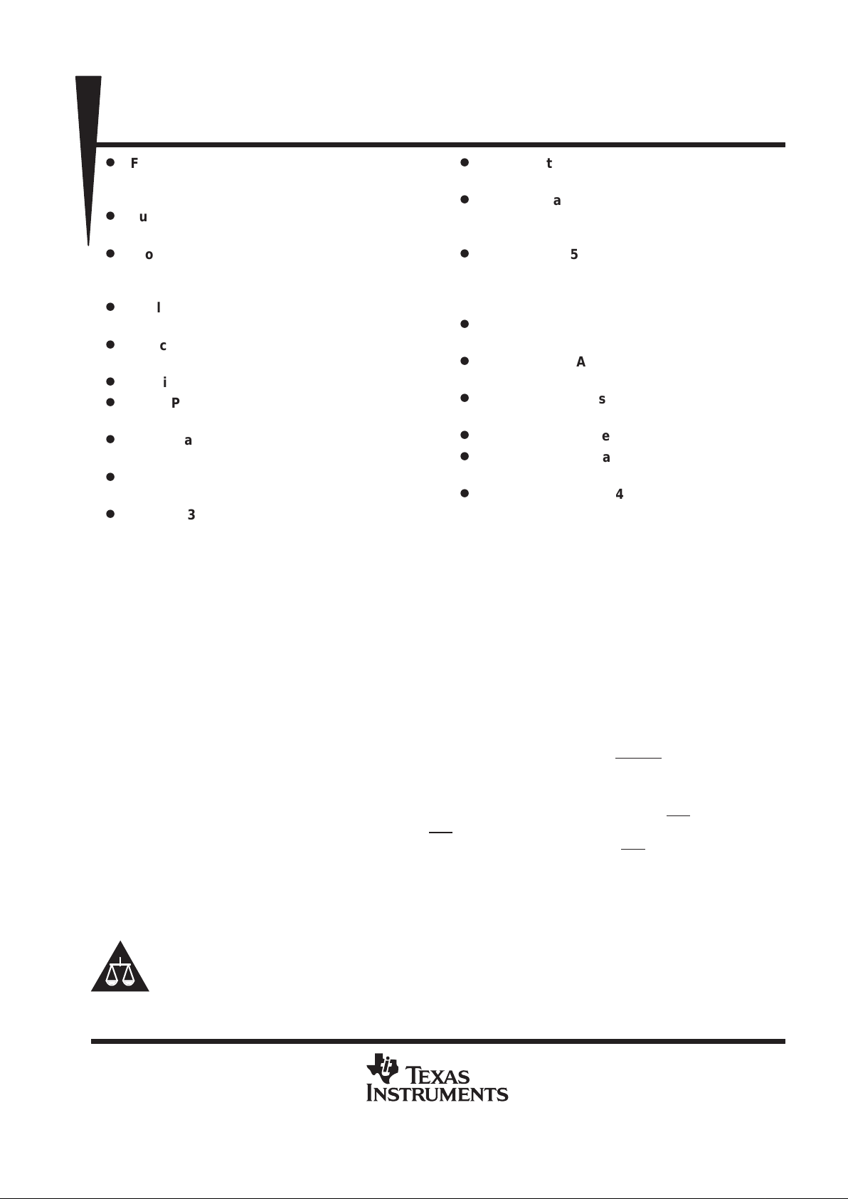
functional block diagram
Link
Interface
I/O
Received
Data
Decoder/
Retimer
Arbitration
and
Control
State
Machine
Logic
CPS
LPS
CNA
SYSCLK
LREQ
CTL0
CTL1
D0
D1
Cable Port 1
Transmit
Data
Encoder
Crystal
Oscillator,
PLL
System, and
Clock
Generator
Bias
Voltage
and
Current
Generator
R0
R1
TPBIAS1
TPA1+
TPA1–
TPB1+
TPB1–
XI
XO
FILTER
PC0
PC1
PC2
C/LKON
TESTM1
TESTM2
PD
RESET
ISO
D2
D3
TPBIAS2
TPBIAS3
TPA2+
TPA2–
TPB2+
TPB2–
Cable Port 2
TPA3+
TPA3–
TPB3+
TPB3–
Cable Port 3
TSB21LV03C
IEEE 1394-1995 TRIPLE-CABLE TRANSCEIVER/ARBITER
SLLS331A – FEBRUARY 1999 – REVISED OCTOBER 1999
5
POST OFFICE BOX 655303 • DALLAS, TEXAS 75265
package outline
17 18 19
TPBIAS3
TPBIAS2
TPBIAS1
TPA1+
TPA1–
TPB1+
TPB1–
AGND
TPA2+
TPA2–
TPB2+
TPB2–
TPA3+
TPA3–
TPB3+
TPB3–
48
47
46
45
44
43
42
41
40
39
38
37
36
35
34
33
20
1
2
3
4
5
6
7
8
9
10
11
12
13
14
15
16
RESET
LPS
LREQ
V
DD
-5V
DV
DD
DV
DD
PD
DGND
SYSCLK
DGND
CTL0
CTL1
D0
D1
D2
D3
21 22 23 24
AGND
FILTER
63 62 61 60 5964 58
ISO
AGNDR1R0
XO
XI
AGND
C/LKON
PC2
PC1
TESTM2
TESTM1
CPS
56 55 5457
25 26 27 28 29
53 52
PLLGND
PLLGND
51 50 49
30 31 32
PC0
CNA
AGND
AGND
DGND
DGND
DV
DDDVDD
AVDDAV
DD
AV
DD
AV
DD
PLLV
DD
DGND
DGND
TSB21LV03C
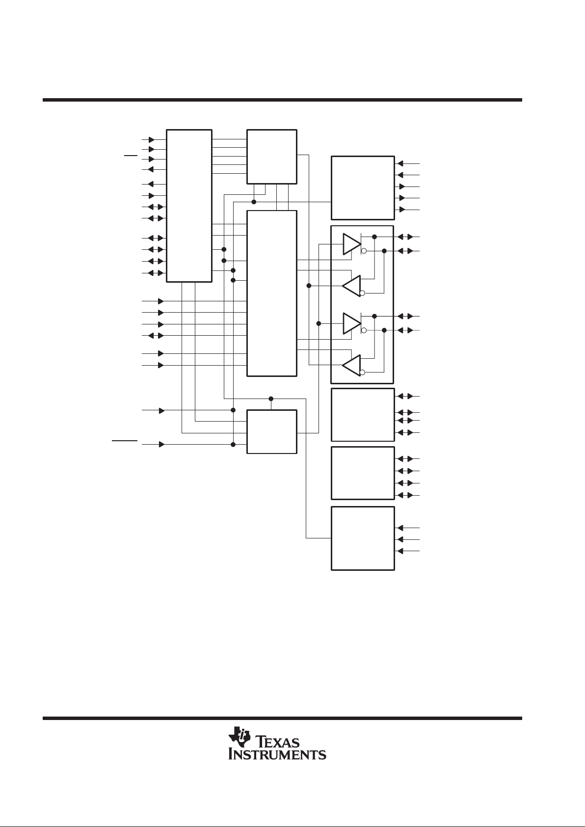
PLASTIC QUAD FLATPACK (PM)
(TOP VIEW)
TSB21LV03C
IEEE 1394-1995 TRIPLE-CABLE TRANSCEIVER/ARBITER
SLLS331A – FEBRUARY 1999 – REVISED OCTOBER 1999
6
POST OFFICE BOX 655303 • DALLAS, TEXAS 75265
28 29
TPBIAS3
TPBIAS2
TPBIAS1
TPA1+
TPA1–
TPB1+
TPB1–
AGND
AGND
TPA2+
TPA2–
TPB2+
TPB2–
TPA3+
TPA3–
TPB3+
TPB3–
30
10
11
12
13
14
15
16
17
18
19
20
21
22
23
24
25
26
RESET
LPS
LREQ
V
DD
–5V
DV
DD
DV
DD
PD
DGND
DGND
SYSCLK
DGND
CTL0
CTL1
D0
D1
D2
D3
31 32 33 34
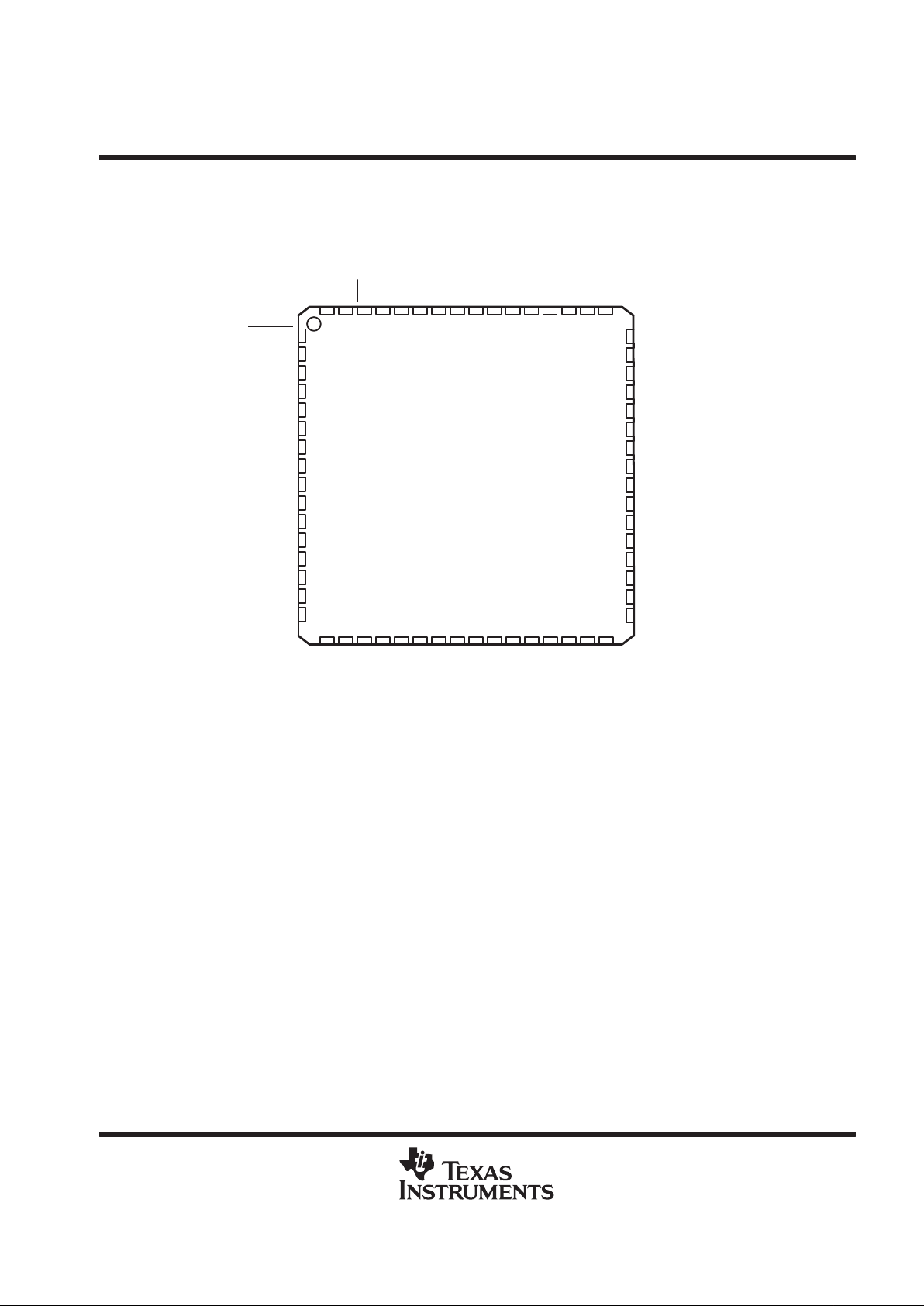
CERAMIC QUAD FLATPACK (HV)
(TOP VIEW)
X1
AV
87 65493
ISO
AGND
AGNDR1R0
PLL V
X0
AGND
AGND
C/LKON
PC2
DV
DV
TESTM2
TESTM1
CPS
AV
AV
168672
35 36 37 38 39
66 65
27
DGND
DGND
FILTER
PLLGND
64 63 62 61
40 41 42 43
PC1
PC0
CNA
AGND
PLLGNDAVAGND
AGND
DGND
DGND
60
59
58
57
56
55
54
53
52
51
50
49
48
47
46
45
44
DD
DD
DD
DD
DD
DD
DD
AVAILABLE OPTIONS
PACKAGE
T
A
PLASTIC QUAD
FLAT PACK
(PM)
CERAMIC QUAD
FLAT PACK
(HV)
0°C to 70°C TSB21LV03CPM —
–40°C to 85°C TSB21LV03CIPM —
–55°C to 125°C — TSB21LV03CMHVB

TSB21LV03C
IEEE 1394-1995 TRIPLE-CABLE TRANSCEIVER/ARBITER
SLLS331A – FEBRUARY 1999 – REVISED OCTOBER 1999
7
POST OFFICE BOX 655303 • DALLAS, TEXAS 75265
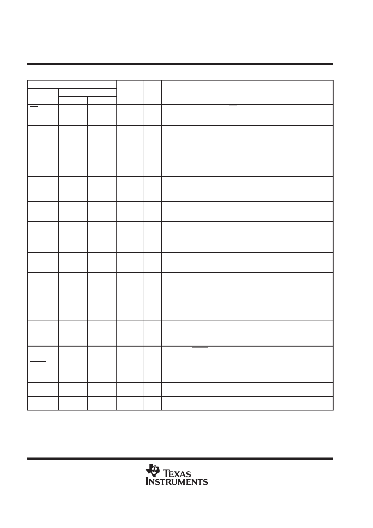
Terminal Functions
TERMINAL
NO.
TYPE I/O DESCRIPTION
NAME
HV PM
AGND 5, 6, 36,
37, 43, 52,
53, 61, 62
26, 32, 41,
49, 50, 61
Supply — Analog circuit ground. All AGND terminals should be tied together to the
low-impedance circuit-board ground plane. External to the device, AGND
should be tied to DGND and PLLGND.
AV
DD
34, 35,
63, 67
24, 25,
51, 55
Supply — Analog circuit power. A combination of high frequency decoupling capacitors
near each AVDD terminal is suggested, such as 0.1-µF and 0.001-µF capacitors.
Lower frequency 10-µF filtering capacitors are also recommended. AV
DD
terminals are separated from DVDD terminals internally from the other supply
terminals to provide noise isolation. They should be tied together to a power
plane on the circuit board. Each supply source should be individually filtered.
C/LKON 38 27 CMOS I/O
Bus manager capable (input). When set as an input, C/LKON specifies in the
Self-ID packet that the node is bus manager capable. The bit value programming
is done by tying the terminal through a 10-kΩ resistor to VDD (high, bus manager
capable) or to GND (low, not bus manager capable). Using either the pullup or
pulldown resistor allows the LINK ON output to override the input bit value when
necessary.
Link-on (output). When set as an output, C/LKON indicates the reception of a
link-on message by asserting a 6.114-MHz signal.
CNA 42 31 CMOS O Cable-not-active output. CNA is asserted high when none of the TSB21L V03C
ports are connected to another active port. This circuit remains active during the
power-down mode.
CPS 33 23 CMOS I Cable power status. CPS is normally connected to the cable power through a
400-kΩ resistor. This circuit drives an internal comparator that detects the
presence of cable power. This information is maintained in two internal registers
and is available to the LLC by way of a register read (see the Phy-Link Interface
Annex in the IEEE 1394-1995 standard).
CTL0
CTL1
21
22
11
12
CMOS I/O Control I/O. The CTLn terminals are bidirectional communications control
signals between the TSB21LV03C and the LLC. These signals control the
passage of information between the two devices. Control I/O terminals are 5-V
tolerant. The CTLn terminals have an internal bus-holder function built-in.
D0 – D3 23, 24,
25, 26
13, 14,
15, 16
CMOS I/O Data I/O. The D terminals are bidirectional and pass data between the
TSB21LV03C and the LLC. Data I/O terminals are 5-V tolerant. The D terminals
have an internal bus-holder function built-in.
DGND 8, 9, 17,
18, 20,
27, 28
8, 10, 17,
18, 63, 64
Supply — Digital circuit ground. The DGND terminals should be tied to the low-impedance
circuit-board ground plane. External to the device, AGND should be tied to
DGND and PLLGND.
DV
DD
14, 15,
29, 30
5, 6,
19, 20
Supply — Digital circuit power. DVDD supplies power to the digital portion of the device. It is
recommended that a combination of high-frequency decoupling capacitors be
connected to DVDD (i.e., paralleled 0.1 µF and 0.001 µF). Lower frequency
10-µF filtering capacitors can also be used. These supply terminals are
separated from A VDD internally in the device to provide noise isolation. These
terminals should also be tied together to a power plane on the circuit board.
Individual filtering networks for each is desired.
FILTER 66 54 CMOS I/O PLL filter. FILTER is connected to a 0.1-µF capacitor and then to PLLGND to
complete the internal lag-lead filter . This filter is required for stable operation of
the frequency multiplier PLL running off of the crystal oscillator.
TSB21LV03C
IEEE 1394-1995 TRIPLE-CABLE TRANSCEIVER/ARBITER
SLLS331A – FEBRUARY 1999 – REVISED OCTOBER 1999
8
POST OFFICE BOX 655303 • DALLAS, TEXAS 75265
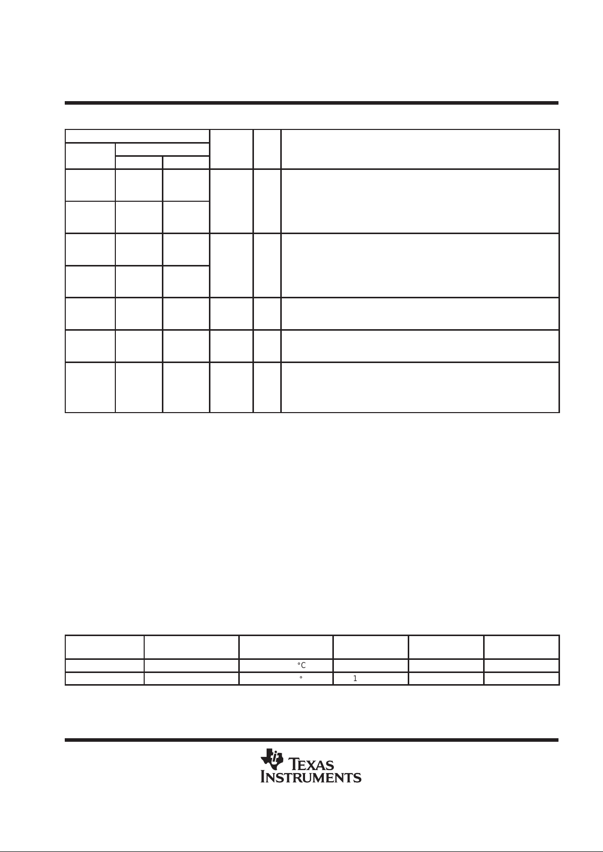
Terminal Functions (Continued)
TERMINAL
NO.
TYPE I/O DESCRIPTION
NAME
HV PM
ISO
7 62 CMOS I Link interface isolation input. ISO is normally tied high both to implement TI
bus-holder isolation or no isolation. The TSB21L V03C does not support Annex J
isolation.
LPS 11 2 CMOS I Link power status. LPS is connected to either the VDD supplying the LLC through
a 1–k Ω resistor or directly to a pulsed output that is active when the LLC is
powered for the purpose of monitoring the LLC power status. The pulsed signal
must be between 220 kHz and 5.5 MHz to be sensed as active. If LPS is inactive,
the phy-LLC interface is disabled, and the TSB21L V03C performs only the basic
repeater functions required for network initialization and operation. LPS is 5-V
tolerant and has an internal bus-holder function built-in. If this terminal is tied
through a resistor to a fixed state, the resistor must be 1 kΩ or less.
LREQ 12 3 CMOS I Link request. LREQ is an input from the LLC that requests the TSB21LV03C to
perform some service. LREQ is 5-V tolerant and has an internal bus-holder
function built-in. If this terminal is tied through a resistor to a fixed state, the
resistor must be 1 kΩ or less.
PC2 – PC0 39, 40, 41 28, 29, 30 CMOS I Power class indicators. The PC signals set the bit values of the three
power-class bits in the Self-ID packet (bits 21, 22, and 23). These bits can be
programmed by tying the terminals to VDD (high) or to GND (low).
PD 16 7 CMOS I Power down. When asserted high, PD turns off all internal circuitry except the
CNA monitor circuits that drive the CNA terminal. PD is 5-V tolerant. The PD
terminal may be tied directly to VDD or to DGND. If this terminal is tied through a
resistor to a fixed state, the resistor must be 1 kΩ or less. The PD terminal has an
internal bus-holder function built in to it.
PLLGND 64, 65 52, 53 Supply —
PLL circuit ground. The PLLGND terminals should be tied to the low-impedance
circuit-board ground plane. External to the device, AGND should be tied to
DGND and PLLGND.
PLLV
DD
2 58 Supply —
PLL circuit power. PLL VDD supplies power to the PLL portion of the device. It is
recommended that a combination of high-frequency decoupling capacitors be
connected to
PLLVDD (i.e., paralleled 0.1 µF and 0.001 µF). Lower frequency 10-µF filtering
capacitors can also be used. The PLLVDD supply terminals are separated from
AVDD and DVDD internally in the device to provide noise isolation. The PLLVDD,
AVDD, and DVDD terminals should also be tied together to a power plane on the
circuit board. Individual filtering networks for each is recommended.
R0
R1
3
4
59
60
— —
Current setting resistor. An internal reference voltage is applied to a resistor connected between R0 and R1 to set the operating current and the cable driver output current. A resistance of 6.3 kΩ ±0.5% should be used to meet the IEEE
1394-1995 standard requirements for output voltage limits.
RESET
10 1 CMOS I
Reset. When RESET is asserted low (active), a bus reset condition is set on the
active cable ports and the the internal logic is reset to the reset start state. An
internal pullup resistor, which is connected to VDD, is provided so only an external delay capacitor is required. This input is a standard logic buffer and can also
be driven by an open-drain logic output buffer . The minimum hold time for RESET is listed in the recommended operating characteristics table.
SYSCLK 19 9 CMOS O
System clock. SYSCLK provides a 49.152-MHz clock signal, which is synchronized with the data transfers to the LLC.
TESTM1
TESTM2
32
31
22
21
CMOS I
Test mode control. TESTM1 and TESTM2 are used during the manufacturing
test and should be tied to VDD.
TSB21LV03C
IEEE 1394-1995 TRIPLE-CABLE TRANSCEIVER/ARBITER
SLLS331A – FEBRUARY 1999 – REVISED OCTOBER 1999
9
POST OFFICE BOX 655303 • DALLAS, TEXAS 75265
Terminal Functions (Continued)
TERMINAL
NO.
TYPE I/O DESCRIPTION
NAME
HV PM
TPA1+
TPA2+
TPA3+
57
51
47
45
40
36
Portn, port cable pair A. TPAn is the port A connection to the twisted-pair cable.
p
p
TPA1–
TPA2–
TPA3–
56
50
46
44
39
35
Cable
O
Board traces from these terminals should be kept matched and as short as pos
-
sible to the external load resistors and to the cable connector.
TPB1+
TPB2+
TPB3+
55
49
45
43
38
34
Portn, port cable pair B. TPBn is the port B connection to the twisted-pair cable.
p
p
TPB1–
TPB2–
TPB3–
54
48
44
42
37
33
Cable
O
Board traces from these terminals should be kept matched and as short as pos
-
sible to the external load resistors and to the cable connector.
TPBIAS1
TPBIAS2
TPBIAS3
58
59
60
46
47
48
Cable O
Portn, twisted-pair bias. TPBIASn provides the 1.86-V nominal bias voltage
needed for proper operation of the twisted-pair cable drivers and receivers and
for sending a valid cable connection signal to the remote nodes.
VDD–5V 13 4 Supply —
5-V VDD supply. VDD–5V should be connected to the LLC VDD supply when a 5-V
LLC is connected to the phy, and it should be connected to the phy DVDD when a
3-V LLC is used.
XI
XO
68
1
56
57
— —
Crystal oscillator. XO and XI connect to a 24.576-MHz parallel resonant fundamental mode crystal. Although, when a 24.576-MHz crystal oscillator is used, it
can be connected to XI with XO left unconnected. The optimum values for the
external shunt capacitors are dependent on the specifications of the crystal
used. See application note on crystal oscillator.
absolute maximum ratings over operating free-air temperature range (unless otherwise noted)
†
Supply voltage range, V
DD
–0.3 V to 4 V. . . . . . . . . . . . . . . . . . . . . . . . . . . . . . . . . . . . . . . . . . . . . . . . . . . . . . . . . .
Input voltage range, V
I
–0.5 V to VDD+0.5 V. . . . . . . . . . . . . . . . . . . . . . . . . . . . . . . . . . . . . . . . . . . . . . . . . . . . . . .
Output voltage range at any output, V
O
–0.5 V to VDD+0.5V. . . . . . . . . . . . . . . . . . . . . . . . . . . . . . . . . . . . . . . . .
Continuous total power dissipation See Dissipation Rating Table. . . . . . . . . . . . . . . . . . . . . . . . . . . . . . . . . . . . . .
Operating free-air temperature, T
A
, TSB21LV03C 0°C to 70°C. . . . . . . . . . . . . . . . . . . . . . . . . . . . . . . . . . . . . . . .
TSB21L V03CI –40°C to 85°C. . . . . . . . . . . . . . . . . . . . . . . . . . . . . . . . . . . . .
TSB21L V03CM –55°C to 125°C. . . . . . . . . . . . . . . . . . . . . . . . . . . . . . . . . . .
Junction temperature, TJ, PM package 150°C. . . . . . . . . . . . . . . . . . . . . . . . . . . . . . . . . . . . . . . . . . . . . . . . . . . . . .
HV package 165°C. . . . . . . . . . . . . . . . . . . . . . . . . . . . . . . . . . . . . . . . . . . . . . . . . . . . . .
Storage temperature range, T
stg
–65°C to 150°C. . . . . . . . . . . . . . . . . . . . . . . . . . . . . . . . . . . . . . . . . . . . . . . . . . . .
Lead temperature 1,6 mm (1/16 inch) from case for 10 seconds 220°C. . . . . . . . . . . . . . . . . . . . . . . . . . . . . . . .
†
Stresses beyond those listed under “absolute maximum ratings” may cause permanent damage to the device. These are stress ratings only, and
functional operation of the device at these or any other conditions beyond those indicated under “recommended operating conditions” is not
implied. Exposure to absolute-maximum-rated conditions for extended periods may affect device reliability.
DISSIPATION RATING TABLE
PACKAGE
TA ≤ 25°C
POWER RATING
DERATING FACTOR
‡
ABOVE TA = 25°C
TA = 70°C
POWER RATING
TA = 85°C
POWER RATING
TA = 125°C
POWER RATING
PM 1866 mW
14.9 mW/_C
1194 mW 972 mW —
HV 2943 mW
21.02 mW/_C
1997 mW 1681 mW 841 mW
‡
This is the inverse of the traditional junction-to-ambient thermal resistance (R
θJA
) and uses a board-mounted 67°C/W for PM package and
47.57°C/W for HV package.

TSB21LV03C
IEEE 1394-1995 TRIPLE-CABLE TRANSCEIVER/ARBITER
SLLS331A – FEBRUARY 1999 – REVISED OCTOBER 1999
10
POST OFFICE BOX 655303 • DALLAS, TEXAS 75265
recommended operating conditions
MIN NOM MAX UNIT
pp
Source power node 3 3.3 3.6
Suppl
y v
oltage, V
DD
Nonsource power node
§
2.7 3 3.6
V
p
p
Commercial 0.7V
DD
High-level input voltage, V
IH
CMOS inputs
Industrial, Military 0.85V
DD
V
Low-level input voltage, V
IL
CMOS inputs 0.2V
DD
V
Cable inputs, 100-Mbit operation 142 260
Differential input voltage, V
ID
Cable inputs, 200-Mbit operation 132 260
mV
Cable inputs, during arbitration 171 262
TPB cable inputs, 100-Mbit or speed signaling off, Source
power node
1.165 2.515
p
TPB cable inputs, 100-Mbit or speed signaling off,
Nonsource power node
§
1.165 2.015
Common-mode input voltage, V
IC
TPB cable inputs, 200-Mbit speed signaling, Source power
node
0.935 2.515
V
TPB cable inputs, 200-Mbit speed signaling, Nonsource
power node
§
0.935 2.015
p
TPA, TPB cable inputs, 100-Mbit operation *±1.08
Receive input jitter
TPA, TPB cable inputs, 200-Mbit operation *±0.5
ns
p
Between TPA and TPB cable inputs, 100-Mbit operation *±0.8
Receive input sle
w
Between TPA and TPB cable inputs, 200-Mbit operation *±0.55
ns
Output current, IOL/I
OH
Control, Data, CNA and C/LKON outputs, SYSCLK –12 12 mA
Output current, I
O
TPBIAS outputs –3 1.3 mA
Hold time, power-up reset (RESET) *2 ms
§
For a node that does not source power (see Section 4.2.2.2 in IEEE 1394–1995 Standard).
* These parameters are not production tested for the HV package.
electrical characteristics over recommended operating conditions (unless otherwise noted)
driver
PARAMETER TEST CONDITION MIN TYP MAX UNIT
V
OD
Differential output voltage 55-Ω load 172 265 mV
V
(OFF)
Off-state differential output voltage Drivers disabled 20 mV
I
O(diff)
Differential current (TPA+, TPA–, TPB+, TPB–) Driver enabled, Speed signaling off –1.05
†
1.05†mA
I
(SP)
Common-mode speed signaling current
(TPB+, TPB–)
200-Mbit speed signaling enabled –2.53
‡
–4.84‡mA
†
Limits are defined as the algebraic sum of TPA+ and TPA– driver currents. Limits also apply to TPB+ and TPB– as the algebraic sum of driver
currents.
‡
Limits are defined as the absolute limit of each of TPB+ and TPB– driver currents.

TSB21LV03C
IEEE 1394-1995 TRIPLE-CABLE TRANSCEIVER/ARBITER
SLLS331A – FEBRUARY 1999 – REVISED OCTOBER 1999
11
POST OFFICE BOX 655303 • DALLAS, TEXAS 75265
electrical characteristics over recommended operating conditions (unless otherwise noted)
(continued)
receiver
PARAMETER TEST CONDITION MIN TYP MAX UNIT
V
IT
Input threshold voltage –30 30 mV
V
IT
Cable bias-detect input threshold voltage, TPBn cable inputs Driver disabled 0.6 1 V
I
IC
Common-mode input current Driver disabled –40 40 µA
15 kΩ
ZIDDiff
erential input impedance
Dri
ver disable
d
*6 pF
p
20 kΩ
ZICCommon-mode impedance
Driver disabled
*24 pF
* These parameters are not production tested for the HV package.
device
PARAMETER TEST CONDITIONS MIN TYP MAX UNIT
V
= 3.3 V
Node transmitting
or repeating
114 mA
I
Supply current
DD
Node receiving 140 mA
DD
y
VDD = 3.6 V *175
VDD = 3.6 V, Power-down mode 20
mA
V
IT
Power status input threshold voltage (CPS) RL = 400 kΩ 4.7 7.5 V
V
OH
High-level output voltage VDD = min, IOH max VDD–0.55 V
V
OL
Low-level output voltage VDD = max, IOL min 0.5 V
I
I
Input current (TESTM1, TESTM2, PC0, PC1, PC2) VI = VDD or 0 ±1 µA
Off-state output current
(CTL0, CTL1, D0, D1, D2, D3, C/LKON)
VO = VDD or 0 ±5 µA
I
off
p
V
= 0 or
Commercial –90 –45 –10
Pullup current (RESET)
I
1.5 V
Industrial, Military –110 –45 –10
µ
A
V
TH+
Positive arbitration comparator-input threshold voltage 89 168 mV
V
TH–
Negative arbitration comparator-input threshold
voltage
–168 –89 mV
V
IT
Speed-signal input threshold voltage
TPBIAS –TPA common-mode
voltage
49 131 mV
V
O
Output voltage (TPBIAS1, TPBIAS2, TPBIAS3) At rated IO current 1.665 2.015 V
Bus holding current (LPS, LREQ, CTLn, Dn, PD) VI = 1/2(VDD) 725 µA
* These parameters are not production tested for the HV package.
thermal characteristics
PARAMETER TEST CONDITIONS MIN TYP MAX UNIT
PM package
67
°
R
θJA
Junction-to-free-air thermal resistance
HV package
EIA/JESD51-3, No air flo
w
47.57
°C/W
PM package 10.4
°
R
θJC
Junction-to-case thermal resistance
HV package 3
°C/W

TSB21LV03C
IEEE 1394-1995 TRIPLE-CABLE TRANSCEIVER/ARBITER
SLLS331A – FEBRUARY 1999 – REVISED OCTOBER 1999
12
POST OFFICE BOX 655303 • DALLAS, TEXAS 75265
switching characteristics
PARAMETER MEASURED TEST CONDITIONS MIN TYP MAX UNIT
Jitter, transmit TPA, TPB ±0.25 ns
Skew rate, transmit Between TPA and TPB *±0.15 ns
t
r
Rise time, transmit 10% to 90% RL = 55 Ω, CL = 10 pF *2.2 ns
t
f
Fall time, transmit 90% to 10% RL = 55 Ω, CL = 10 pF *2.2 ns
t
su
Setup time, Dn, CTLn, LREQ↑↓ to
SYSCLK↑
50% to 50% See Figure 1 *5 ns
t
h
Hold time, Dn, CTLn, LREQ↑↓ before
SYSCLK↑
50% to 50% See Figure 1 *2 ns
t
d
Delay time, SYSCLK↑ to Dn, CTLn↑↓ 50% to 50% See Figure 2 2 11 ns
* These parameters are not production tested for the HV package.
PARAMETER MEASUREMENT INFORMATION
t
su
t
h
SYSCLK
Dn, CTLn, LREQ
50%
50%50%
Figure 1. Dn, CTLn, LREQ Input Setup and Hold Timing Waveforms
t
d
SYSCLK
Dn, CTLn
50%
50%
Figure 2. Dn and CTLn Output-Delay Timing Waveforms

TSB21LV03C
IEEE 1394-1995 TRIPLE-CABLE TRANSCEIVER/ARBITER
SLLS331A – FEBRUARY 1999 – REVISED OCTOBER 1999
13
POST OFFICE BOX 655303 • DALLAS, TEXAS 75265
APPLICATION INFORMATION
internal register configuration
The accessible internal registers of this device are listed in Table 1.
Table 1. Internal Register Configuration
Address 0 1 2 3 4 5 6 7
0000 Physical ID R CPS
0001 RHB IBR GC
0010 SPD Rev NP
0011 AStat1 BStat1 Ch1 Con1 Reserved
0100 AStat2 BStat2 Ch2 Con2 Reserved
0101 AStat3 BStat3 Ch3 Con3 Reserved
0110 LoopInt CPSInt CPS IR Reserved C
0111 Reserved
1000 Reserved
Table 2. Internal Register Field Descriptions
FIELD SIZE TYPE DESCRIPTION
ÁÁ
Á
ÁÁ
Á
ÁÁ
Á
ÁÁ
Á
AStat(n)
Á
Á
Á
Á
Á
Á
Á
Á
2
Á
Á
Á
Á
Á
Á
Á
Á
Read
only
AStat contains the line state of TPAn. The status is indicated by the following:
11 = high-impedance state
01 = 1
10 = 0
00 = Invalid data state. Power-up reset initializes to this line state. This line state is also output during transmit
and receive operations, including date-end signaling. The line state outputs are generally valid during arbitration
and idle conditions on the bus.
ÁÁ
Á
ÁÁ
Á
ÁÁ
Á
BStat(n)
Á
Á
Á
Á
Á
Á
2
Á
Á
Á
Á
Á
Á
Read
only
BStat contains the line state of TPBn. The status is indicated by the following:
11 = high-impedance state
01 = 1
10 = 0
00 = Invalid data state. Power-up reset initializes to this line state. This line state is also output during transmit
and receive operations. The line state outputs are generally valid during arbitration and idle conditions on the bus.
C 1 R Bus manager capable. C indicates the state of the Bus Manager Capable input. When set, this bit is used by
the TSB21LV03C to specify in the Self-ID packet that the node is Bus Manager Capable.
Ch(n)
1
Read
only
When Ch = 1, the port is a child, otherwise it is a parent. This bit is invalid after a hardware reset or a bus reset
until tree-ID processing is completed.
ÁÁ
Á
ÁÁ
Á
ÁÁ
Á
ÁÁ
Á
ÁÁ
Á
ÁÁ
Á
Con(n)
Á
Á
Á
Á
Á
Á
Á
Á
Á
Á
Á
Á
1
Á
Á
Á
Á
Á
Á
Á
Á
Á
Á
Á
Á
Read
only
Con indicates the connection status of the port. When Con = 1, the port is connected, otherwise it is disconnected.
This bit is set to 1 by a hardware reset and is updated to reflect the actual cable connection status of the port during
bus reset. The TSB21LV03C contains connection debounce circuitry that prevents a new cable connection on
a port from initiating a bus reset until the connection status has been stable for at least 335 ms. A cable disconnect
initiates a bus reset immediately . After a hardware reset, the TSB21LV03C sets the connection status of all ports
to 0. The TSB21LV03C proceeds with the bus reset, tree-ID, and Self-ID, but with all ports considered to be
disconnected child ports. The TSB21L V03C can not transmit any signals on the serial bus ports during this time.
The TSB21LV03C does report itself as root with a physical address of 00h at the completion of Self-ID. If any port
is actually connected, after the debounce delay, the TSB21LV03C initiates another bus reset, which proceeds
normally with interaction between the TSB21L V03C and its peer nodes.

TSB21LV03C
IEEE 1394-1995 TRIPLE-CABLE TRANSCEIVER/ARBITER
SLLS331A – FEBRUARY 1999 – REVISED OCTOBER 1999
14
POST OFFICE BOX 655303 • DALLAS, TEXAS 75265
APPLICATION INFORMATION
Table 2. Internal Register Field Descriptions (continued)
FIELD SIZE TYPE DESCRIPTION
ÁÁÁ
Á
CPS
Á
Á
1
Á
Á
Read
only
Cable power status (CPS) contains the status of the CPS input terminal. When cable power voltage has
dropped too low for reliable operation, CPS is reset (0). CPS is included twice in the internal registers to
expedite handling of the CPSInt.
CPSInt 1
Read/
Write
CPSint indicates that a cable power status interrupt has occurred. This interrupt occurs whenever the CPS
input goes low. The interrupt indicates that the cable power voltage has dropped too low to ensure reliable
operation. This bit is cleared (0) by a hardware reset or by writing a 0 to this register. However , if the CPS input
is still low, another cable-power status interrupt immediately occurs.
ÁÁÁ
Á
ÁÁÁ
Á
ÁÁÁ
Á
GC
Á
Á
Á
Á
Á
Á
6
Á
Á
Á
Á
Á
Á
Read/
Write
The gap count (GC) register sets the fair and arb-reset gap times. The gap count may be set to a particular
value to optimize bus performance. Typically, the gap count should be set to 2 times the maximum number
of hops on the bus and must be set to the same value for all nodes on the bus. The gap count can be set by
either a write to this register or by reception or transmission of a PHY_CONFIG packet. The gap count is reset
to 3Fh after a hardware reset or after two consecutive bus resets without an intervening write to the gap count
register (either a write to the gap count register by the LLC or a PHY_CONFIG packet).
IBR 1
Read/
Write
When set, initiate bus reset (IBR) causes the current node to immediately initiate a bus reset. IBR is cleared
(0) after a hardware reset or a bus reset.
IR
1
Read/
Write
IR indicates that the last bus reset was initiated in this TSB21LV03C phy . This bit is also included in the self-ID
packet.
ÁÁÁ
Á
LoopInt
Á
Á
1
Á
Á
Read/
Write
LoopInt indicates that a configuration loop timeout has occurred. This interrupt occurs when the arbitration
controller waits for too long a period of time during tree-ID. This interrupt can indicate that the bus is configured
in a loop. This bit is cleared (0) by a hardware reset or by writing a 0 to this register bit.
ÁÁÁ
Á
NP
Á
Á
4
Á
Á
Read
only
NP contains the number of ports implemented in the core logic (not the number of ports actually on the device).
For the TSB21LV03C, NP is set to 0011b.
ÁÁÁ
Á
Physical ID
Á
Á
6
Á
Á
Read
only
Physical ID contains the physical address of the local node. The physical ID in valid after a hardware reset or
a bus reset until the Self-ID process has been completed. A complete Self-ID is indicated by an unsolicited
status transfer of the register 0 contents to the LLC.
ÁÁÁ
Á
R
Á
Á
1
Á
Á
Read
only
R indicates whether the current node is the root node or not. This bit is cleared (0) on a hardware reset or a
bus reset. This bit is set during tree-ID when the current node is root.
Rev
2
Read
only
The revision (Rev) bits indicate the design revision of the core logic. For the TSB21LV03C, Rev is set to 00.
ÁÁÁ
Á
RHB
Á
Á
1
Á
Á
Read/
Write
When set, the root hold-off bit (RHB) instructs the local node to try to become the root node during the next
bus reset. RHB is reset (0) during a hardware reset and is not affected by a bus reset.
ÁÁÁ
Á
SPD
Á
Á
2
Á
Á
Read
only
The speed (SPD) bits indicates the top signaling speed of the local port and for the TSB21LV03C is set to 01b.

TSB21LV03C
IEEE 1394-1995 TRIPLE-CABLE TRANSCEIVER/ARBITER
SLLS331A – FEBRUARY 1999 – REVISED OCTOBER 1999
15
POST OFFICE BOX 655303 • DALLAS, TEXAS 75265
APPLICATION INFORMATION
Cable Port
55 Ω
55 Ω
5 kΩ
TPBIASn
TPAn+
TPAn–
TPBn+
TPBn–
1 µF
TSB21LV03C
220 pF
55 Ω
55 Ω
CPS
400 kΩ
–+
AGND
DGND
PLLGND
Cable
Power
Pair
Cable
Pair
A
Cable
Pair
B
Figure 3. Twisted-Pair Cable Interface Connections
LPS
LPS
Link Power
Square Wave Input
1 kΩ
1 kΩ
Figure 4. Nonisolated Connection Variations for LPS

TSB21LV03C
IEEE 1394-1995 TRIPLE-CABLE TRANSCEIVER/ARBITER
SLLS331A – FEBRUARY 1999 – REVISED OCTOBER 1999
16
POST OFFICE BOX 655303 • DALLAS, TEXAS 75265
APPLICATION INFORMATION
1 MΩ
0.001 µF0.01 µF
Outer Cable Shield
Chassis Ground
Figure 5. Compliant DC Isolated Outer Shield Termination
Outer Shield Termination
Chassis Ground
Figure 6. Nonisolated Outer Shield Termination

TSB21LV03C
IEEE 1394-1995 TRIPLE-CABLE TRANSCEIVER/ARBITER
SLLS331A – FEBRUARY 1999 – REVISED OCTOBER 1999
17
POST OFFICE BOX 655303 • DALLAS, TEXAS 75265
APPLICATION INFORMATION (PM PACKAGE)
17 18 19 20 21 22 23 24
AGND
FILTER
63 62 61 60 5964 58
ISO
AGND
R1
R0
XO
XI
AGND
C/LKON
PC2
PC1
TESTM2
TESTM1
CPS
56 55 5457
25 26 27 28 29
53 52
PLLGND
PLLGND
51 50 49
30 31 32
PC0
CNA
AGND AGND
DGND
DGND
DVDDDV
DD
AVDDAV
DD
AV
DD
AV
DD
PLLV
DD
DGND
DGND
TSB21LV03C, CI
48
TPBIAS3
47
TPBIAS2
46
TPBIAS1
45
TPA1+
44
TPA1–
43
TPB1+
42
TPB1–
41
AGND
40
TPA2+
39
TPA2–
38
TPB2+
37
TPB2–
36
TPA3+
35
TPA3–
34
TPB3+
33
TPB3–
1
RESET
2
LPS
3
LREQ
4
VDD-5V
5
DV
DD
6
DV
DD
7
PD
8
DGND
9
SYSCLK
10
DGND
11
CTL0
12
CTL1
13
D0
14
D1
15
D2
16
D3
6.34 kΩ
±0.5%
V
DD
33 pF
33 pF
V
DD
24.576 MHz
0.1 µF
V
DD
0.1 µF
Link Pulse
or V
DD
LLC Interface
Link V
DD
V
DD
Power Down
LLC Interface
TPBIASTP CABLESTP CABLES
V
DD
400 kΩ
Cable Power
10 kΩ
V
DD
Power-Class
Programming
Bus
Manager
LKON
CNA OUT
V
DD
1 MΩ
±0.5%
NOTE A: For more information see the application note.
Figure 7. External Component Connections

TSB21LV03C
IEEE 1394-1995 TRIPLE-CABLE TRANSCEIVER/ARBITER
SLLS331A – FEBRUARY 1999 – REVISED OCTOBER 1999
18
POST OFFICE BOX 655303 • DALLAS, TEXAS 75265
APPLICATION INFORMATION (HV PACKAGE)
28 29
TPBIAS3
TPBIAS2
TPBIAS1
TPA1+
TPA1–
TPB1+
TPB1–
AGND
AGND
TPA2+
TPA2–
TPB2+
TPB2–
TPA3+
TPA3–
TPB3+
TPB3–
30
10
11
12
13
14
15
16
17
18
19
20
21
22
23
24
25
26
RESET
LPS
LREQ
VDD–5V
DV
DD
DV
DD
PD
DGND
DGND
SYSCLK
DGND
CTL0
CTL1
D0
D1
D2
D3
31 32 33 34
X1
AV
87 6 5493
ISO
AGND
AGND
R1
R0
PLLV
X0
AGND
AGND
C/LKON
PC2
DV
DV
TESTM2
TESTM1
CPS
AV
AV
168672
35 36 37 38 39
66 65
27
DGND
DGND
FILTER
PLLGND
64 63 62 61
40 41 42 43
PC1
PC0
CNA
AGND
PLLGND
AV
AGND
AGND
DGND
DGND
60
59
58
57
56
55
54
53
52
51
50
49
48
47
46
45
44
DD
DD
DD
DD
DD
DD
DD
0.1 µF
Link Pulse
or V
DD
LLC Interface
Link V
DD
V
DD
Power Down
LLC Interface
V
DD
400 kΩ
Cable Power
10 kΩ
V
DD
Power-Class
Programming
Bus
Manager
LKON
CNA OUT
TPBIASTP CABLESTP CABLES
6.34 kΩ
±0.5%
V
DD
33 pF
33 pF
V
DD
24.576 MHz
0.1 µF
V
DD
V
DD
1 MΩ
±0.5%
NOTE A: For more information see the application note.
Figure 8. External Component Connections

TSB21LV03C
IEEE 1394-1995 TRIPLE-CABLE TRANSCEIVER/ARBITER
SLLS331A – FEBRUARY 1999 – REVISED OCTOBER 1999
19
POST OFFICE BOX 655303 • DALLAS, TEXAS 75265
APPLICATION INFORMATION
crystal selection
TI PHYs may use an external 24.576 MHz crystal connected between the XI and XO pins on the PHY to provide
the PHY clock. The following are some typical specifications for the crystals used with the Physical Layers from
TI. The clock resulting from the input from the crystal must be within the tolerance of ±100 parts per million for
the PHYs to function correctly. This is required by the 1394 standard. This frequency tolerance for the PHY
clocks on each node must be maintained over the variation introduced over production runs of boards and
environment the machines operate in. Every board must have an SYSCLK (clock generated by the PHY) within
±100 ppm of 49.152 MHz to be compliant to the 1394 standard. If adjacent nodes are more than 200 ppm away
from one another then long packets sent across the 1394 bus may be corrupted, with the final bits of the packet
being lost. TI PHYs are designed with a maximum of margin, but the limits imposed by 1394 must still be adhered
to.
1. Crystal Mode of operation:
Fundamental
2. Frequency Tolerance at 25°C:
T otal variation specification for the complete circuit is 100ppm. The crystal is specified at less than 100 ppm.
3. Frequency stability (over temperature):
T otal variation specification for the complete circuit is 100 ppm. The crystal is specified at less than 100 ppm.
NOTE:
The total variation must be kept below 100 ppm with some allowance for variation introduced by
variations in board builds and device tolerances. So the sum of the frequency tolerance and the
frequency stability must be less than 100 ppm. This can be traded off between the two, for example
the frequency tolerance may be specified at 50 ppm and the temperature may be specified at
30 ppm to give a total of 80 ppm possible variation just due to the crystal.
4. Load capacitance: [Parallel (pF)]
Parallel mode crystal circuits should be used for optimum precision. Load capacitance will be a function of
your board layout and circuit. The total load capacitance (C
L
) will affect the frequency of oscillation. Consult
with the crystal vendor on design to get an SYSCLK supplied by the PHY to less than 100 ppm from
49.152 MHz . A tolerance of ±5% is recommend for load capacitors. For TI’s TSBKOHCI403 Designer Kit
with a crystal specified for 20-pF loading, a value of 33 pF for each load capacitor (C9 = C10 below) is
appropriate with the layout used for the board. The load specified for the crystal includes the load capacitors
(C9, C10), the loading of the PHY pins (C
PHY
), and the loading of the board itself (CBD). T o summarize: C
L
=[ (C9 × C10) / (C9+C10)] + C
PHY
+ CBD. Representative values for C
PHY
are ~1 pF and for CBD are about
0.8 pF per centimeter of board etch, a typical board can have from 3 pF to 6 pF or more. The capacitance
of load capacitors C9 and C10 combine as capacitors in series.

TSB21LV03C
IEEE 1394-1995 TRIPLE-CABLE TRANSCEIVER/ARBITER
SLLS331A – FEBRUARY 1999 – REVISED OCTOBER 1999
20
POST OFFICE BOX 655303 • DALLAS, TEXAS 75265
APPLICATION INFORMATION
crystal selection (continued)
C10
X1
XI
XO
24.567 MHz
Is
C9
C
PHY
+ C
BD
Figure 9. Load Capacitance for the TSB21LV03C PHY
NOTE:
The layout of the crystal portion of the PHY circuit is important for getting the correct frequency from
the crystal, minimizing the noise introduced into the PHY Phase Lock Loop, and minimizing any
emissions from the circuit. The crystal and the two load capacitors should be considered a unit
during layout. The crystal and the load capacitors should be placed as close as possible to one
another while minimizing the loop area created by the combination of the three components.
Varying the size of the capacitors may help in this. Minimizing the loop area minimizes the effect
of the resonant current (Is) that flows in this resonant circuit. This layout unit (crystal and load
capacitors) should then be placed as close as possible to the PHY XI and XO pins to minimize etch
lengths.
C10
X1
C9
Figure 10. Recommended Crystal and Capacitor Layout for the TSB21LV03C PHY
Part of the verification process for the design should be to measuring the frequency of the SYSCLK output of
the PHY. This should be done with a frequency counter with an accuracy of 6 digits or better. If the SYSCLK
is more than the crystal tolerance away from 49.152 MHz, the load capacitance of the crystal may be varied
to reduce total variation to below 100 ppm. Changes should be done to both load capacitors (C9 and C10 above)
at the same time to the same value. Consult crystal vender for detailed understanding of requirements. In order
for a 1394 bus to operate correctly each SYSCLK on each node on the bus must be within 200 ppm of the
adjacent SYSCLK on the bus. The 1394 standard requires this by specifying a center frequency of 49.152 MHz
and a ±100 ppm tolerance around 49.152 MHz.

TSB21LV03C
IEEE 1394-1995 TRIPLE-CABLE TRANSCEIVER/ARBITER
SLLS331A – FEBRUARY 1999 – REVISED OCTOBER 1999
21
POST OFFICE BOX 655303 • DALLAS, TEXAS 75265
PRINCIPLES OF OPERATION
The TSB21LV03C is designed to operate with a LLC such as the TI TSB12LV22, TSB12LV41, TSB12LV01,
TSB12LV21, TSB12LV31, and TSB12C01. Details of how the LLC devices operate are described in the LLC
data sheets. The following paragraphs describe the operation of the phy-LLC interface.
The TSB21LV03C supports 100-/200-Mbit/s data transfer and has four bidirectional data lines, D0 – D3,
crossing the interface. In 100-Mbit/s operation only D0 and D1 terminals are used. In 200 Mbit/s operation, all
Dn terminals are used for data transfer. The unused Dn terminals are driven low. In addition, there are two
bidirectional control lines CTL0 and CTL1, the 49.152-MHz SYSCLK line from the phy to the LLC, and the LLC
request terminal LREQ from the LLC to the phy . The TSB21LV03C has control of all bidirectional terminals. The
LLC is allowed to drive these terminals only after it has been given permission by the phy . The dedicated LREQ
request terminal is used by the LLC for any activity that it wishes to initiate.
There are four operations that may occur in the phy-LLC interface: request, status, transmit, and receive. With
the exception of the request operation, all actions are initiated by the phy.
When the phy has control of the bus the CTL0 and CTL1 lines are encoded as shown in Table 3.
Table 3. CTLn Status When Phy Has Control of the Bus
CTL0 CTL1 STATUS NAME DESCRIPTION
0 0 Idle No activity is occurring (this is the default mode).
0 1 Status Status information is being sent from the phy to the LLC.
1 0 Receive An incoming packet is being sent from the phy to the LLC.
1 1 Transmit The LLC has been given control of the bus to send an outgoing packet.
When the LLC has control of the bus (phy permission) the CTL0 and CTL1 terminals are encoded as shown
in Table 4.
Table 4. CTLn Status When LLC Has Control of the Bus
CTL0 CTL1 STATUS NAME DESCRIPTION
0 0 Idle The LLC releases the bus (transmission has been completed).
0 1
Hold
The LLC is holding the bus while data is being prepared for transmission or is sending another packet without
arbitrating.
1 0 Transmit An outgoing packet is being sent from the LLC to the phy.
1 1 Reserved None
request
When the LLC requests the bus or accesses a register that is located in the TSB21LV03C, a serial stream of
information is sent across the LREQ line. The length of the stream varies depending on whether the transfer
is a bus request, a read command, or a write command. Regardless of the type of transfer, a start bit of 1 is
required at the beginning of the stream, and a stop bit of 0 is required at the end of the stream. Bit 0 is the most
significant bit, and is transmitted first. The LREQ terminal is required to idle low (logic level 0).

TSB21LV03C
IEEE 1394-1995 TRIPLE-CABLE TRANSCEIVER/ARBITER
SLLS331A – FEBRUARY 1999 – REVISED OCTOBER 1999
22
POST OFFICE BOX 655303 • DALLAS, TEXAS 75265
PRINCIPLES OF OPERATION
Table 5. LLC Bus-Request or Register-Access-Request Bit Length
REQUEST TYPE NUMBER OF BITS
Bus request 7
Read register request 9
Write register request 17
For a Bus Request the length of the LREQ data stream is 7 bits as shown in Table 6.
Table 6. LLC Bus Request
BIT(S) NAME DESCRIPTION
0 Start Bit Indicates the beginning of the transfer (always 1).
1–3 Request Type Indicates the type of bus request (see Table 9 for the encoding of this field).
4–5 Request Speed Should be 00 for TSB21LV03C 100-Mbit/s speed and 01 for 200-Mbit/s speed.
6 Stop Bit Indicates the end of the transfer (always 0).
For a Read Register Request the length of the LREQ data stream is 9 bits as shown in Table 7.
Table 7. LLC Read Register Access
BIT(S) NAME DESCRIPTION
0 Start Bit Indicates the beginning of the transfer (always 1).
1–3 Request Type Always a 100 indicating that this is a read register request.
4–7 Address Identifies the address of the phy register to be read.
8 Stop Bit Indicates the end of the transfer (always 0).
For a Write Register Request the Length of the LREQ data stream is 17 bits as shown in Table 8.
Table 8. LLC Write Register Access
BIT(S) NAME DESCRIPTION
0 Start Bit Indicates the beginning of the transfer (always 1).
1–3 Request Type Always a 101 indicating that this is a write register request.
4–7 Address Identifies the address of the phy register to be written to.
8–15 Data Gives the data that is to be written to the specified register address.
16 Stop Bit Indicates the end of the transfer (always 0).
The 3-bit Request Type field has the values shown in Table 9.
Table 9. LLC Bus Request Type
LREQ1 LREQ2 LREQ3 NAME DESCRIPTION
0 0 0 ImmReq Immediate request. Upon detection of an idle, the LLC takes control of the bus immediately (no
arbitration).
0 0 1 IsoReq Isochronous request: the LLC arbitrates for the bus, no gaps.
0 1 0 PriReq Priority request: the LLC arbitrates after a subaction gap, ignores fair protocol.
0 1 1 FairReq Fair request: the LLC arbitrates after a subaction gap, follows fair protocol.
1 0 0 RdReg The LLC returns the specified register contents through a status transfer.
1 0 1 WrReg The LLC writes to the specified register.
1 1 0 Reserved Reserved
1 1 1 Reserved Reserved

TSB21LV03C
IEEE 1394-1995 TRIPLE-CABLE TRANSCEIVER/ARBITER
SLLS331A – FEBRUARY 1999 – REVISED OCTOBER 1999
23
POST OFFICE BOX 655303 • DALLAS, TEXAS 75265
PRINCIPLES OF OPERATION
LREQ timing (each cell represents one clock sample time):
LR0 LR1 LR2 LR3 LR(n-2) LR(n-1)
NOTE B: Each cell represents one clock sample time.
Figure 11. LREQ Timing
For fair or priority access, the LLC requests control of the bus at least one clock after the phy-LLC interface
becomes idle. If the LLC senses that the CTLn terminals are in a receive state (CTL0 = 1, CTL1 = 0), this
indicates that its request has been lost. This is true anytime during or after the LLC sends the bus request
transfer. Additionally, the phy ignores any fair or priority requests if it asserts the receive state while the LLC is
requesting the bus. The LLC then reissues the request one clock after the next interface idle.
The cycle master uses a normal priority request to send a cycle-start message. After receiving a cycle-start
message, the LLC can issue an isochronous bus request. When arbitration is won, the LLC proceeds with the
isochronous transfer of data. The isochronous request register is cleared in the phy once the LLC sends another
type of request or when the isochronous transfer has been completed. The isochronous request must be issued
during a packet reception. Generally this request would be during reception of a cycle-start packet.
The ImmReq request is issued when the LLC needs to send an acknowledgment after reception of a packet
addressed to it. This request must be issued during packet reception. This is done to minimize the delays that
a phy would have to wait between the end of a packet and the transmittal of an acknowledgment. As soon as
the packet ends, the phy immediately grants access of the bus to the LLC. The LLC sends an acknowledgment
to the sender unless the header CRC of the packet turns out to be bad. In this case, the LLC releases the bus
immediately; it is not allowed to send another type of packet on this grant. To guarantee this, the LLC is forced
to wait 160 ns after the end of the packet is received. The phy then gains control of the bus and the
acknowledgement with the CRC error is sent. Then the bus is released and allowed to proceed with another
requests.
Although highly improbable, it is conceivable that two separate nodes can believe that an incoming packet is
intended for them. The nodes then issue a ImmReq request before checking the CRC of the packet. Since both
phys seize control of the bus at the same time, a temporary, localized collision of the bus occurs somewhere
between the competing nodes. This collision would be interpreted by the other nodes on the network as being
a high-impedance line state, not a bus reset. As soon as the two nodes check the CRC, the mistaken node drops
its request and the false line state is removed. The only side effect would be the loss of the intended
acknowledgment packet (this is handled by the higher-layer protocol).
read/write requests
When the LLC requests to read the specified register contents, the phy sends the contents of the register to the
LLC through a status transfer. When an incoming packet is received while the phy is transferring status
information to the LLC, the phy continues to attempt to transfer the contents of the register until it is successful.
For write requests, the phy loads the data field into the appropriately addressed register as soon as the transfer
has been completed. The LLC is allowed to request read or write operations at any time.

TSB21LV03C
IEEE 1394-1995 TRIPLE-CABLE TRANSCEIVER/ARBITER
SLLS331A – FEBRUARY 1999 – REVISED OCTOBER 1999
24
POST OFFICE BOX 655303 • DALLAS, TEXAS 75265
PRINCIPLES OF OPERATION
status
A status transfer is initiated by the phy when it has status information to transfer to the LLC. The phy waits until
the interface is idle before starting the transfer. The transfer is initiated by asserting the following on the control
terminals: CTL0 – CTL1 = 01 along with the first two bits of status information on the D0 – D3 terminals. The
phy maintains CTL0 – CTL1 = 01 for the duration of status transfer. The phy may prematurely end a status
transfer by asserting something else other than CTL0 – CTL1 = 01 on the control terminals. This could be caused
by an incoming packet from another node. The phy continues to attempt to complete the transfer until the
information has been successfully transmitted. There must be at least one idle cycle in between consecutive
status transfers.
The phy normally sends just the first 4 bits of status to the LLC. These bits are status flags that are needed by
the LLC state machines. The phy sends an entire status packet to the LLC after a request transfer that contains
a read request, or when the phy has pertinent information to send to the LLC or transaction layers. The only
defined condition where the phy automatically sends a register to the LLC is after self-ID, when it sends the
physical-ID register, which contains the new node address. After a power-on reset, the TSB21L V03C sends two
self-ID status transfers. The first transfer is invalid (a status of not connected); later, during the same bus reset,
a second, correct root, node number, and connection status self-ID is transferred. During all other bus resets,
only one Self-ID status is transmitted.
The definition of the bits in the status transfer are shown in Table 10 and the timing is shown in Figure 7.
Table 10. 16-Bit Stream Status Request
BIT(S) NAME DESCRIPTION
0 Arbitration Reset Gap Bit 0 indicates that the phy has detected that the bus has been idle for an arbitration reset gap time (this time
is defined in the IEEE 1394–1995 standard). Bit 0 is used by the LLC in its busy/retry state machine.
1 Subaction Gap Bit 1 indicates that the phy has detected that the bus has been idle for a subaction gap time (this time is
defined in the IEEE 1394–1995 standard). Bit 1 is used by the LLC to detect the completion of an isochro-
nous cycle.
2 Bus Reset Bit 2 indicates that the phy has entered the bus reset state.
3 State Timeout or CPS Bit 3 indicates that the phy stayed in a particular state for too long a period, which is usually the effect of a
loop in the cable topology, or that the cable power has dropped below the threshold for reliable operation.
4–7 Address Bits 4 – 7 hold the address of the phy register whose contents are transferred to the LLC.
8–15 Data Bits 8 – 15 contain the data that is to be sent to the LLC.
00 01 01 01 00 00
Phy
CTL0, CTL1
00 S[0,1] 00 00
Phy
D0, D1
S[2,3] S[14,15]
Figure 12. Status Transfer Timing

TSB21LV03C
IEEE 1394-1995 TRIPLE-CABLE TRANSCEIVER/ARBITER
SLLS331A – FEBRUARY 1999 – REVISED OCTOBER 1999
25
POST OFFICE BOX 655303 • DALLAS, TEXAS 75265
PRINCIPLES OF OPERATION
transmit
When the LLC wants to transmit information, it first requests access to the bus through the LREQ terminal. Once
the phy receives this request, it arbitrates to gain control of the bus. When the phy wins ownership of the serial
bus, it grants the bus to the LLC by asserting the transmit state on the CTLn terminals for at least one SYSCLK
cycle, followed by idle for one clock cycle. The LLC takes control of the bus by asserting either hold or transmit
on the CTLn terminals. Hold is used by the LLC to keep control of the bus when it needs some time to prepare
the data for transmission. The phy keeps control of the bus for the LLC by asserting a data-on state on the bus.
It is not necessary for the LLC to use hold when it is ready to transmit as soon as bus ownership is granted.
When the LLC is prepared to send data, it asserts the transmit state on the CTLn terminals as well as sending
the first bits of the packet on the D0 – D3 lines (assuming 200 Mbits/s). The transmit state is held on the CTLn
terminals until the last bits of data have been sent. The LLC then asserts an idle state on the CTLn terminals
for one clock cycle after which it releases control of the interface.
However, there are times when the LLC needs to send another packet without releasing the bus. For example,
the LLC may want to send consecutive isochronous packets or it may want to attach a response to an
acknowledgment. To do this, the LLC asserts a hold state instead of an idle state when the first packet of data
has been completely transmitted. In this case, hold informs the phy that the LLC needs to send another packet
without releasing control of the bus. The phy then waits a set amount of time before asserting a transmit state.
The LLC can then proceed with the transmittal of the second packet. After all data has been transmitted and
the LLC has asserted an idle state on the CTLn terminals, the phy asserts its own idle state on the CTLn
terminals. When sending multiple packets in this fashion, it is required that all data be transmitted at the same
speed. This is required because the transmission speed is set during arbitration and since the arbitration step
is skipped, there is no way of informing the network of a change in speed.
11 00 ZZ ZZ ZZ ZZ
Phy
CTL0, CTL1
ZZ ZZ 00ZZ ZZ00
0000 0000 ZZZZ ZZZZ ZZZZ ZZZZ
Phy
D0 – D3
ZZZZ ZZZZ 0000ZZZZ ZZZZ0000
ZZ ZZ 01 10 10 10
LLC
CTL0, CTL1
00 00 ZZ01 10ZZ
ZZZZ ZZZZ 0000 D0 D1 D2
LLC
D0 – D3
0000 0000 ZZZZ0000 DnZZZZ
Single Packet
ZZ ZZ 00 11 00 ZZ
Phy
CTL0, CTL1
ZZ ZZ ZZ00ZZ
Continued Packet
ZZ
ZZZZ ZZZZ 0000 0000 0000 ZZZZ
Phy
D0 – D3
ZZZZ ZZZZ ZZZZ0000ZZZZZZZZ
01 00 ZZ ZZ ZZ 01
LLC
CTL0, CTL1
01 10 10ZZ1010
0000 0000 ZZZZ ZZZZ ZZZZ 0000
LLC
D0 – D3
0000 D0 D1ZZZZDnDn-1
NOTE A: ZZ = High-impedance state
D0 => Dn = Packet data
Figure 13. Transmit Timing Waveforms

TSB21LV03C
IEEE 1394-1995 TRIPLE-CABLE TRANSCEIVER/ARBITER
SLLS331A – FEBRUARY 1999 – REVISED OCTOBER 1999
26
POST OFFICE BOX 655303 • DALLAS, TEXAS 75265
PRINCIPLES OF OPERATION
receive
When data is received by the phy from the serial bus, the phy transfers the data to the LLC for further processing.
The phy asserts a receive state on the CTLn terminals and asserts a 1 on each Dn terminal. The phy indicates
the start of the packet by placing the speed code on the data bus. The phy then proceeds with the transmittal
of the packet to the LLC on the Dn terminals while still keeping the receive status on the CTLn terminals. Once
the packet has been completely transferred, the phy asserts an idle state on the CTLn terminals, which
completes the receive operation.
NOTE:
The speed is a phy-LLC protocol and not included in the CRC.
10 10 10 10
Phy
CTL0, CTL1
10 00 001000
1111 SPD D0 D1
Phy
D0 – D3
Dn 0000 000011110000
NOTE A: SPD = Speed Code
D0 => Dn = Packet data
Figure 14. Receive Timing Waveforms
Table 11. Speed Code for the Receiver
D0 – D3 Data Rate
00YY
†
100 Mbit/s
0100 200 Mbit/s
†
Y = Transmitted as 0, ignored on receive.
power class bits in self-ID packet
T able 12 describes the meaning of the power-class bits in the pwr field of the Self-ID packet. Bit 21 is transmitted
first, followed by bit 22 and then bit 23. This power-field bit description complies with the IEEE 1394-1995
standard.
Table 12. Self-ID Packet Pwr-Field Bit Description
PC0–PC2 DESCRIPTION
000 Node does not need power and does not repeat power.
001 Node is self powered, and provides a minimum of 15 W to the bus.
010 Node is self powered, and provides a minimum of 30 W to the bus.
011 Node is self powered, and provides a minimum of 45 W to the bus.
100 Node may be powered from the bus, and is using up to 1 W.
101 Node may be powered from the bus, and is using up to 1 W. An additional 2 W is needed to enable the LLC and higher layers.
110 Node may be powered from the bus, and is using up to 1 W . An additional 5 W is needed to enable the LLC and higher layers.
111 Node may be powered from the bus, and is using up to 1 W. An additional 9 W is needed to enable the LLC and higher layers.

TSB21LV03C
IEEE 1394-1995 TRIPLE-CABLE TRANSCEIVER/ARBITER
SLLS331A – FEBRUARY 1999 – REVISED OCTOBER 1999
27
POST OFFICE BOX 655303 • DALLAS, TEXAS 75265
MECHANICAL INFORMATION
PM (S-PQFP-G64) PLASTIC QUAD FLA TPACK
4040152/C 11/96
32
17
0,13 NOM
0,25
0,45
0,75
Seating Plane
0,05 MIN
Gage Plane
0,27
33
16
48
1
0,17
49
64
SQ
SQ
10,20
11,80
12,20
9,80
7,50 TYP
1,60 MAX
1,45
1,35
0,08
0,50
M
0,08
0°–7°
NOTES: A. All linear dimensions are in millimeters.
B. This drawing is subject to change without notice.
C. Falls within JEDEC MS-026
D. May also be thermally enhanced plastic with leads connected to the die pads.

MECHANICAL DATA
MCFP013A – JANUARY 1995 – REVISED OCTOBER 1996
28
POST OFFICE BOX 655303 • DALLAS, TEXAS 75265
MECHANICAL INFORMATION
HV (S-GQFP-F68) CERAMIC QUAD FLA TPACK
0.400 (10,16) TYP
4040072/C 04/96
0.485 (12,32)
0.500 (12,70)
0.009 (0,229)
0.013 (0,330)
SQ
SQ
1.500 (38,10)
1.300 (33,02)
0.152 (3,86)
0.128 (3,25)
0.005 (0,127)
0.007 (0,178)
9
61
60 44
43
27
2610
1
0.025 (0,635)
NOTES: A. All linear dimensions are in inches (millimeters).
B. This drawing is subject to change without notice.
C. This package can be hermetically sealed with a ceramic lid using glass frit.

IMPORTANT NOTICE
T exas Instruments and its subsidiaries (TI) reserve the right to make changes to their products or to discontinue
any product or service without notice, and advise customers to obtain the latest version of relevant information
to verify, before placing orders, that information being relied on is current and complete. All products are sold
subject to the terms and conditions of sale supplied at the time of order acknowledgement, including those
pertaining to warranty, patent infringement, and limitation of liability.
TI warrants performance of its semiconductor products to the specifications applicable at the time of sale in
accordance with TI’s standard warranty. Testing and other quality control techniques are utilized to the extent
TI deems necessary to support this warranty. Specific testing of all parameters of each device is not necessarily
performed, except those mandated by government requirements.
CERT AIN APPLICATIONS USING SEMICONDUCTOR PRODUCTS MAY INVOLVE POTENTIAL RISKS OF
DEATH, PERSONAL INJURY, OR SEVERE PROPERTY OR ENVIRONMENTAL DAMAGE (“CRITICAL
APPLICATIONS”). TI SEMICONDUCTOR PRODUCTS ARE NOT DESIGNED, AUTHORIZED, OR
WARRANTED TO BE SUITABLE FOR USE IN LIFE-SUPPORT DEVICES OR SYSTEMS OR OTHER
CRITICAL APPLICATIONS. INCLUSION OF TI PRODUCTS IN SUCH APPLICA TIONS IS UNDERSTOOD T O
BE FULLY AT THE CUSTOMER’S RISK.
In order to minimize risks associated with the customer’s applications, adequate design and operating
safeguards must be provided by the customer to minimize inherent or procedural hazards.
TI assumes no liability for applications assistance or customer product design. TI does not warrant or represent
that any license, either express or implied, is granted under any patent right, copyright, mask work right, or other
intellectual property right of TI covering or relating to any combination, machine, or process in which such
semiconductor products or services might be or are used. TI’s publication of information regarding any third
party’s products or services does not constitute TI’s approval, warranty or endorsement thereof.
Copyright 1999, Texas Instruments Incorporated
 Loading...