

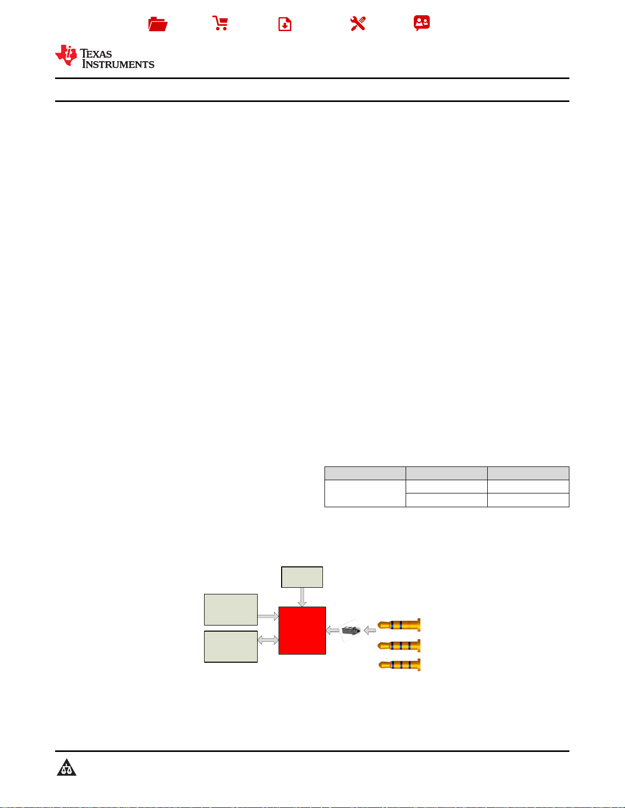
BATTERY
Application
Processor
TS3A227E
Audio Codec
L
R
G
L
R
G M
L
R
GM
Product
Folder
Sample &
Buy
Technical
Documents
Tools &
Software
Support &
Community
SCDS358B –NOVEMBER 2014–REVISED FEBRUARY 2015
TS3A227E Autonomous Audio Accessory Detection and Configuration Switch
1 Features 3 Description
1
• Supple Range of 2.5 V to 4.5 V
• Accessory Insertion/Removal Detection with
Adjustable De-bounce Timings
• Accessory Configuration Detection:
– Stereo 3-pole Headphone
– 4-pole Standard Headset with MIC on Sleeve
– 4-pole OMTP Headset with MIC on Ring2
• Key Press Detection for Up to 4 Keys
• Ultra Low Ground FET RONof 60 mΩ
• Power Off Noise Removal
• Isolation of MICBIAS From Audio Jack to Remove
Click/Pop Noise
• Integrated Codec Sense Line
• Manual I2C Control
• FM Transmission Capability
• Dual Small Package Options
– 16 Pin DSBGA
– 16 Pin QFN
2 Applications
• Mobile Phones
• Tablets
• Notebooks and Ultrabooks
• Anywhere a 3.5 mm Audio Jack is Used
The TS3A227E is an autonomous audio accessory
detection and configuration switch that detects 3-pole
or 4-pole audio accessories and configures internal
switches to route the signals accordingly.
The internal ground FETS of the TS3A227E have an
ultra-low RONof 60 mΩ to minimize crosstalk impact.
The ground FETs are also designed to pass FM
signals, making it possible to use the ground line of
the accessory as an FM antenna in mobile audio
applications.
Internal isolation switches allow the TS3A227E to
remove the click/pop noise that can be generated
during and insertion or removal of an audio
accessory. In addition depletion FETs prevent a
floating ground while the device is unpowered,
removing the humming noise present when leaving
accessories plugged into an unpowered system.
A low-power sleep mode is provided which shuts
down internal circuitry to achieve very low quiescent
current draw when no headset is inserted.
The TS3A227E features integrated key press
detection for detecting up to 4 keys with press and
release support.
Manual I2C control allows the TS3A227E to adapt to
application needs by providing control over debounce settings and switch states.
Device Information
PART NUMBER PACKAGE BODY SIZE (NOM)
TS3A227E
(1) For all available packages, see the orderable addendum at
the end of the datasheet.
TS3A227E
(1)
QFN (16) 3.50 mm × 3.50 mm
DSBGA (16) 1.79 mm × 1.79 mm
4 Simplified Schematic
1
An IMPORTANT NOTICE at the end of this data sheet addresses availability, warranty, changes, use in safety-critical applications,
intellectual property matters and other important disclaimers. PRODUCTION DATA.

TS3A227E
SCDS358B –NOVEMBER 2014–REVISED FEBRUARY 2015
www.ti.com
Table of Contents
1 Features.................................................................. 1
2 Applications ........................................................... 1
3 Description ............................................................. 1
4 Simplified Schematic............................................. 1
5 Revision History..................................................... 2
6 Pin Configuration and Functions......................... 3
7 Specifications......................................................... 4
7.1 Absolute Maximum Ratings...................................... 4
7.2 ESD Ratings ............................................................ 4
7.3 Recommended Operating Conditions....................... 5
7.4 Thermal Information.................................................. 5
7.5 Electrical Characteristics........................................... 6
7.6 I2C Interface Timing Characteristics ......................... 8
7.7 Timing Diagrams....................................................... 9
7.8 Typical Characteristics............................................ 12
8 Parameter Measurement Information ................ 12
9 Detailed Description ............................................ 17
9.1 Overview ................................................................. 17
9.2 Functional Block Diagram....................................... 18
9.3 Feature Description................................................. 19
9.4 Device Functional Modes........................................ 20
9.5 Register Maps ........................................................ 24
9.6 Register Field Descriptions..................................... 24
10 Application and Implementation........................ 33
10.1 Application Information.......................................... 33
10.2 Typical Application ............................................... 33
11 Power Supply Recommendations..................... 47
12 Layout................................................................... 48
12.1 Layout Guidelines ................................................. 48
12.2 Layout Example (QFN)......................................... 48
12.3 Layout Example (DSBGA).................................... 49
13 Device and Documentation Support................. 50
13.1 Trademarks........................................................... 50
13.2 Electrostatic Discharge Caution............................ 50
13.3 Glossary................................................................ 50
14 Mechanical, Packaging, and Orderable
Information........................................................... 50
5 Revision History
Changes from Revision A (December 2014) to Revision B Page
• Added DSBGA package to the Thermal Information table. ................................................................................................... 5
• Updated SWITCH RESISTANCE for the DSBGA package. ................................................................................................. 6
Changes from Original (July 2014) to Revision A Page
• Initial release of full version document. ................................................................................................................................. 1
2 Submit Documentation Feedback Copyright © 2014–2015, Texas Instruments Incorporated
Product Folder Links: TS3A227E
GND
TIP
GND
SDA
VDD
MICP
GNDA
RING2
SLEEVE
SCL
THERMALPAD
16 15 14 13
5 6 7 8
1
2
3
4
12
11
10
9
RING2_SENSE
SLEEVE_SENSE
GND_SENSE
DET_TRIGGER
MC_PRESENT
INT
4 3 2 1
D
C
B
A
VDD
SLEEVE_
SENSE
GND
INT
SDA
SCL
GND
TIP
RING2
MICP
RING2_
SENSE
MIC_
PRESENT
GND_
SENSE
DET_
TRIGGER
SLEEVE GNDA
www.ti.com
6 Pin Configuration and Functions
TS3A227E
SCDS358B –NOVEMBER 2014–REVISED FEBRUARY 2015
NAME RVA YFF
DET_TRIGGER 15 B1 I/O
GND 1, 2 A2, B2 GND Primary ground connection for the TS3A227E. Must be connected to system ground.
GNDA 11 D2 I/O
GND_SENSE 5 A4 I/O Ground sense line for the codec.
INT 13 C2 GND
MIC_PRESENT 16 A1 I/O Open drain output to indicate to the host that a headset with a microphone is inserted..
MICP 6 B4 I/O Microphone signal connection to the codec. Microphone bias is applied to this pin.
RING2 12 D1 O
RING2_SENSE 7 C4 GND
SCL 9 C3 I
SDA 3 B3 I/O
SLEEVE 10 D3 O
SLEEVE_SENSE 8 D4 GND
THERMAL PAD GND
TIP 14 C1 I/O Connect to the TIP pin of the 3.5 mm jack.
VDD 4 A3 PWR Power input to the TS3A227E. External de-coupling capacitors are required on this pin.
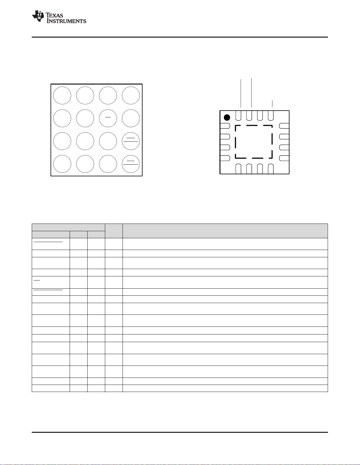
PIN
DSBGA – YFF
Top View
Pin Functions
TYPE DESCRIPTION
A falling edge from high to low on this pin triggers accessory detection. This pin can be connected the
headset jack to allow automatic pull-down to ground after headset insertion to initialize detection.
Ground connection for the internal ground FETs of the TS3A227E. If FM is being supported connect this pin
to the FM matching network. If FM is not being support connect this pin to system ground.
Open drain interrupt output from the TS3A227E to notify the host that an event has occurred. If I2C is not
used this pin must be grounded.
Headset current return path if RING2 is ground for the headset. Connect to 3.5 mm jack RING2 connection
with low DC resistance trace.
Connected to the RING2 pin of the 3.5 mm jack. If RING2 pin on plug in is MIC signal, this is connected to
MICP. If not, this is connected to GND_SENSE and becomes the ground sensing feedback for the accessory
Clock from I2C bus. This can be connected to VDD if I2C is not used.
Bidirectional data from/to I2C bus. This can be connected to VDD if I2C is not used.
Headset current return path if SLEEVE is GND for headset. Connect to 3.5 mm jack SLEEVE connection with
low DC resistance trace.
Connected to the SLEEVE pin of the 3.5 mm jack. If SLEEVE pin on plug in is MIC signal, this is connected to
MICP. If not, this is connected to GND_SENSE and becomes the ground sensing feedback for the accessory
The THERMAL PAD of the RVA – QFN package must be connected to any internal PCB ground plane using
multiple vias for best thermal performance.
QFN – RVA
Top View
Copyright © 2014–2015, Texas Instruments Incorporated Submit Documentation Feedback 3
Product Folder Links: TS3A227E
TS3A227E
SCDS358B –NOVEMBER 2014–REVISED FEBRUARY 2015
www.ti.com
7 Specifications
7.1 Absolute Maximum Ratings
over operating free-air temperature range referenced with respect to GND (unless otherwise noted)
MIN MAX UNIT
Input Voltage VDD –0.3 5 V
SDA, SCL, INT, MIC_PRESENT –0.3 VDD+ 0.5 V
TIP –3.3 VDD+ 0.5 V
DET_TRIGGER –2.2 VDD+ 0.5 V
GND_SENSE, RING2, SLEEVE, RING2_SENSE, SLEEVE_SENSE, –0.3 3.6
MICP, GNDA 0.5
ON-state switch Combined continuous current through R2GNDFET and SLV GNDFET 500 mA
current
Operating ambient temperature range –40 85 °C
T
stg
(1) Stresses beyond those listed under Absolute Maximum Ratings may cause permanent damage to the device. These are stress ratings
only, which do not imply functional operation of the device at these or any other conditions beyond those indicated under Recommended
Operating Conditions. Exposure to absolute-maximum-rated conditions for extended periods may affect device reliability.
(2) This rating is exclusive and the voltage on the pins must not exceed either 3.6 and VDD. E.g. if VDD= 4.5 V the voltage on the pin must
not exceed 3.6 V and if VDDis = 2.5 V the voltage on the pin must not exceed 3.0 V.
Continuous current through R2DFET and SLV DFET 50
Continuous current through S1 20
Continuous current through S2 20
Continuous current through S3PR 50
Continuous current through S3PS 50
Continuous current through S3GR 100
Continuous current through S3GS 100
Storage temperature range –65 150 °C
(1)
(2)
and VDD+ V
7.2 ESD Ratings
VALUE UNIT
V
Human body model (HBM), ESD stress voltagenew note #1 to the ESD
Ratings table and combined MIN MAX column to VALUE
Electrostatic discharge Charged device model (CDM), ESD stress voltage
(ESD)
Contact discharge model (IEC) ESD stress voltage on TIP,
DET_TRIGGER, RING2_SENSE, SLEEVE_SENSE, RING2, SLEEVE
(1) (2)
(1) (3)
(1)
(1) Electrostatic Discharge (ESD) to measure device sensitivity and immunity to damage caused by assembly line electrostatic discharges
into the device
(2) JEDEC document JEP155 states that 500-V HBM allows safe manufacturing with a standard ESD control process.
(3) JEDEC document JEP157 states that 250-V CDM allows safe manufacturing with a standard ESD control process.
±2000 V
±500 V
±8000 V
4 Submit Documentation Feedback Copyright © 2014–2015, Texas Instruments Incorporated
Product Folder Links: TS3A227E
TS3A227E
www.ti.com
SCDS358B –NOVEMBER 2014–REVISED FEBRUARY 2015
7.3 Recommended Operating Conditions
over operating free-air temperature range (unless otherwise noted)
MIN MAX UNIT
VDD Power supply voltage range 2.5 4.5 V
VIDigital input voltage range
VIOInput/output voltage range V
SDA, SCL 0 V
DET_TRIGGER –2.2 V
RING2_SENSE, SLEEVE_SENSE, RING2,
SLEEVE, GND_SENSE, MICP
0 3.3
(1)
TIP –3 V
VOOutput voltage range INT, MIC_PRESENT 0 V
VIHInput logic high
VILInput logic low
T
Operating ambient temperature –40 85 °C
A
SDA, SCL 1.2 V
DET_TRIGGER 0.65 × V
DD
SDA, SCL 0 0.4 V
DET_TRIGGER 0 0.4 × V
DD
DD
and VDD
DD
DD
DD
V
DD
DD
(1) This rating is exclusive and the voltage on the pins must not exceed either 3.3 and VDD. E.g. if VDD= 4.5 V the voltage on the pin must
not exceed 3.3 V and if VDDis = 2.5 V the voltage on the pin must not exceed 2.5 V.
V
V
V
V
V
V
7.4 Thermal Information
TS3A227E TS3A227E
THERMAL METRIC
R
θJA
R
θJC(top)
R
θJB
ψ
JT
ψ
JB
R
θJC(bot)
Junction-to-ambient thermal resistance 45.9 77.9
Junction-to-case (top) thermal resistance 52.6 0.6
Junction-to-board thermal resistance 21.2 12.5
Junction-to-top characterization parameter 0.9 2.3
Junction-to-board characterization parameter 21.2 12.5
Junction-to-case (bottom) thermal resistance 4.3 -
(1) For more information about traditional and new thermal metrics, see the IC Package Thermal Metrics application report, SPRA953.
(1)
RTE YFF UNIT
16 PINS 16 PINS
°C/W
Copyright © 2014–2015, Texas Instruments Incorporated Submit Documentation Feedback 5
Product Folder Links: TS3A227E
TS3A227E
SCDS358B –NOVEMBER 2014–REVISED FEBRUARY 2015
www.ti.com
7.5 Electrical Characteristics
Unless otherwise noted the specification applies over the VDD and ambient operating temperature range.
PARAMETER TEST CONDITIONS MIN TYP MAX UNIT
SUPPLY VOLTAGE
VDD Supplyvoltage 2.5 3.3 4.5 V
No accessory inserted. I2C bus inactive
VDD= 2.5 V to 4.5 V
Manual switch control = ’1’ , I2C bus inactive,
VDD= 2.5 V to 4.5 V, Depletion FETs on
Manual switch control = ’1’ , I2C bus inactive,
VDD= 2.5 V to 4.5 V Depletion FETs off
3-pole accessory inserted.
I
DD
Quiescent current
I2C bus inactive
VDD= 2.5 V to 4.5 V
3-pole accessory inserted.
I2C bus inactive,
(1)
, FM Support = ’0’
(1)
FM Support = ’1’
VDD= 2.5 V to 4.5 V
4-pole Accessory inserted.
I2C bus inactive,
(1)
VDD= 2.5 V to 4.5 V
4-pole Accessory inserted.
I
DD_1.8
Quiescent current addition from using a
1.8 V I2C bus.
(2)
KP detection enabled
I2C bus inactive,
No accessory inserted.
I2C bus inactive at 1.8 V,
VDD= 2.5 V to 4.5 V
(1)
VDD= 2.5 V to 4.5 V
SWITCH RESISTANCE
RING2 GNDFET on resistance (DSBGA
R
R2GNDFT
R
SLVGNDFT
Package)
RING2 GNDFET on resistance (QFN
Package)
SLEEVE GNDFET on resistance (DSBGA
Package)
SLEEVE GNDFET on resistance (QFN
VDD= 3.3 V, V
I
= 75 mA
GNDA
GND
= 0V,
Package)
R
S3PS
R
S3PR
R
S3GS
R
S3GR
R
S1
R
S2
R
R2DFET
R
SLVDFET
S3PS on resistance VDD= 3.3 V, 3 6.5
V
S3PR on resistance 3 6.5
SLEEVE_SENSE/RING2_SENSE
I
= ±10 mA
MICP
S3GS on resistance VDD= 3.3 V, 0.5 1
V
S3GR on resistance 0.5 1
SLEEVE_SENSE/RING2_SENSE
I
GND_SENSE
= ±75 mA
Switch 1 on resistance 15 30
Switch 2 on resistance 15 30
RING2 depletion FET on resistance 75 150
VDD= 3.3 V, I
GND
= 10 mA
SLEEVE depletion FET on resistance 75 150
SWITCH LEAKAGE CURRENT
RING2 pin off leakage 1
SLEEVE pin off leakage 1
I
OFF
RING2_SENSE pin off leakage 1
SLEEVE_SENSE pin off leakage 1
VIN= 0 V to 3.3 V, VDD= 3.3 V µA
MICP pin off leakage 1
GND_SENSE pin off leakage 1
I
ON
S2PS, S3PR, S3GS, S3GR on leakage V
SLEEVE/RING2
= 0V, VDD= 3.3 V 1 µA
(1) The I2C bus is inactive if both the SDA and SCL lines are tied to VDD.
(2) If the I2C bus is operating at 1.8 V the I
(3) The I2C bus is inactive if both the SDA and SCL lines are tied to 1.8 V.
current number will be in addition to the other current consumption numbers specified.
DD_1.8
(3)
= 0 V to 2.7 V, Ω
= 0 V to 2.7 V, Ω
(1)
(1)
0.5 10 µA
7 15 µA
20 40 µA
11 20 µA
25 45 µA
25 40 µA
30 45 µA
1 8 µA
40 85
60 95
40 85
60 95
mΩ
Ω
Ω
6 Submit Documentation Feedback Copyright © 2014–2015, Texas Instruments Incorporated
Product Folder Links: TS3A227E
www.ti.com
SCDS358B –NOVEMBER 2014–REVISED FEBRUARY 2015
Electrical Characteristics (continued)
Unless otherwise noted the specification applies over the VDD and ambient operating temperature range.
PARAMETER TEST CONDITIONS MIN TYP MAX UNIT
SWITCH TIMING
VDD= 2.5 V, 3.3 V, 4.5 V,
RL= 300 Ω, CL= 50 pF
V
SLEEVE_SENSE/RING2_SENSE
3.3 V (VDD= 3.3 V, VDD= 4.5 V)
= 2.5 V (VDD= 2.5 V),
VDD= 2.5 V, 3.3 V, 4.5 V
RPU= 1500 Ω, CL= 50 pF
VPU= 2.5 V (VDD= 2.5 V),
3.3 V (VDD= 3.3 V, VDD= 4.5 V)
VDD= 2.5 V, 3.3 V, 4.5 V
RPU= 1500 Ω, CL= 50 pF
VPU= 2.5 V (VDD= 2.5 V),
3.3 V (VDD= 3.3 V, VDD= 4.5 V)
VDD= 2.5 V, 3.3 V, 4.5 V
RL= 300 Ω, CL= 50 pF
V
SLEEVE_SENSE/RING2_SENSE
3.3 V (VDD= 3.3 V, VDD= 4.5 V)
= 2.5 V (VDD= 2.5 V),
VDD= 2.5 V, 3.3 V, 4.5 V
RPU= 1500 Ω, CL= 50 pF
VPU= 2.5 V (VDD= 2.5 V),
3.3 V (VDD= 3.3 V, VDD= 4.5 V)
VDD= 2.5 V, 3.3 V, 4.5 V
RPU= 1500 Ω, CL= 50 pF
VPU= 2.5 V (VDD= 2.5 V),
3.3 V (VDD= 3.3 V, VDD= 4.5 V)
VDD= 3.3 V, IOL= 10 mA
= 3 mA 0 0.4
OLMAX
SDA, SCL 1.2 V
DET_TRIGGER V
VDDx
0.65
SDA, SCL 0 0.4
DET_TRIGGER 0 VDDx 0.4
VDD= 3.3 V, I
/DET_TRIGGER
= 1 µA 0.5 1 1.85 MΩ
t
OFF
t
ON
DIGITAL I/O
V
OL
V
IH
V
IL
R
PU/DT
Turn off time for S3PS, S3PR, S3GS,
S3GR
Turn off time for S1, S2, RING2 GNDFET,
SLEEVE GNDFET
Turn off time for RING2 DFET and
SLEEVE DFET
Turn on time for S3PS, S3PR, S3GS,
S3GR
Turn on time for S1, S2, RING2 GNDFET,
SLEEVE GNDFET
Turn on time for RING2 DFET and
SLEEVE DFET
MIC_PRESENT low level output voltage 0 0.4
INT low level output voltage 0 0.4 V
SDA low level output voltage VDD= 3.3 V, I
Input logic high V
Input logic low
Internal DET_TRIGGER pull-up
resistance
TS3A227E
5 µs
5 µs
500 µs
1 µs
35 µs
1 µs
DD
DD
Copyright © 2014–2015, Texas Instruments Incorporated Submit Documentation Feedback 7
Product Folder Links: TS3A227E
TS3A227E
SCDS358B –NOVEMBER 2014–REVISED FEBRUARY 2015
www.ti.com
Electrical Characteristics (continued)
Unless otherwise noted the specification applies over the VDD and ambient operating temperature range.
PARAMETER TEST CONDITIONS MIN TYP MAX UNIT
DYNAMIC CHARACTERISTICS
PSR
217
PSR
1k
PSR
20k
ISO
S3
SEP
S3
BW Bandwidth through GNDFETs VIN= 60 mVPP, I
THD
200
THD
500
SNR –90 –110 dB
t
DET
T
power-up
t
REMOVAL
Power supply rejection –85 –110 dB
SLEEVE_SENSE or RING2_SENSE to
MICP Isolation
SLEEVE_SENSE to RING2_SENSE
Separation
MICP to RING2_SENSE or
SLEEVE_SENSE total harmonic
distortion
MICP to RING2_SENSE or
SLEEVE_SENSE signal to noise ratio
Detection sequence duration high to low and INT transition from high to low. 175 210 ms
Power up time Power-up time 20 25 ms
Removal wait period low to high and RING2/SLEEVE DFETs turning 50 65 ms
VDD= 3.3 V ± 200 mVPP, f = 217 Hz, RLat
RING2= 50 Ω
VDD= 3.3 V ± 200 mVPP, f = 1 kHz, RLat
RING2= 50 Ω
VDD= 3.3 V ± 200 mVPP, f = 20 kHz, RLat
RING2= 50 Ω
VIN= 200 mVPP, f = 20 Hz – 20 kHz, RL= 50 Ω –90 dB
VIN= 200 mVPP, f = 20 Hz – 20 kHz, RL= 50 Ω –75 dB
= 10 mA 120 150 MHz
BIAS
VIN= 1.5 V + 200 mVPP, f = 20 Hz – 20 kHz,
RS= 600 Ω, RL= 600 Ω
VIN= 1.5 V + 500 mVPP, f = 20 Hz – 20 kHz,
RS= 600 Ω, RL= 600 Ω
VIN= 1 V
RS= 600 Ω, RL= 600 Ω
Time between DET_TRIGGER transition from
Default 90 ms insertion debounce.
Time from VDD> 2.5 V till I2C communication is
ready
Time between DET_TRIGGER transition from
on
, f = 20 Hz – 20 kHz,
RMS
–95 –120
–70 –90
0.003 %
0.002%
7.6 I2C Interface Timing Characteristics
Unless otherwise noted the specification applies over the VDD and ambient operating temperature range
STANDARD MODE FAST MODE I2C
I2C BUS BUS
MIN MAX MIN MAX
20 + 0.1
Cb
3.45 0.3 0.9 µs
f
scl
t
sch
t
scl
t
sp
t
sds
t
sdh
t
icr
t
icf
t
ocf
t
buf
t
sts
t
sth
t
sps
t
vd(data)
t
vd(ack)
C
b
PARAMETER
I2C clock frequency 0 100 0 400 kHz
I2C clock high time 4 0.6 µs
I2C clock low time 4.7 1.3 µs
I2C spike time 50 50 ns
I2C serial data setup time 250 100 ns
I2C serial data hold time 0 0 ns
I2C input rise time 1000 21 300 ns
I2C input fall time 300 21 300 ns
I2C output fall time; 10 pF to 400 pF bus 300 300 µs
I2C bus free time between Stop and Start 4.7 1.3 µs
I2C Start or repeater Start condition setup time 4.7 0.6 µs
I2C Start or repeater Start condition hold time 4 0.6 µs
I2C Stop condition setup time 4 0.6 µs
Valid data time; SCL low to SDA output valid 3.45 0.3 0.9 µs
Valid data time of ACK condition; ACK signal from SCL low to SDA
(out) low
I2C bus capacitive loading 0 400 0 400 pF
UNIT
8 Submit Documentation Feedback Copyright © 2014–2015, Texas Instruments Incorporated
Product Folder Links: TS3A227E
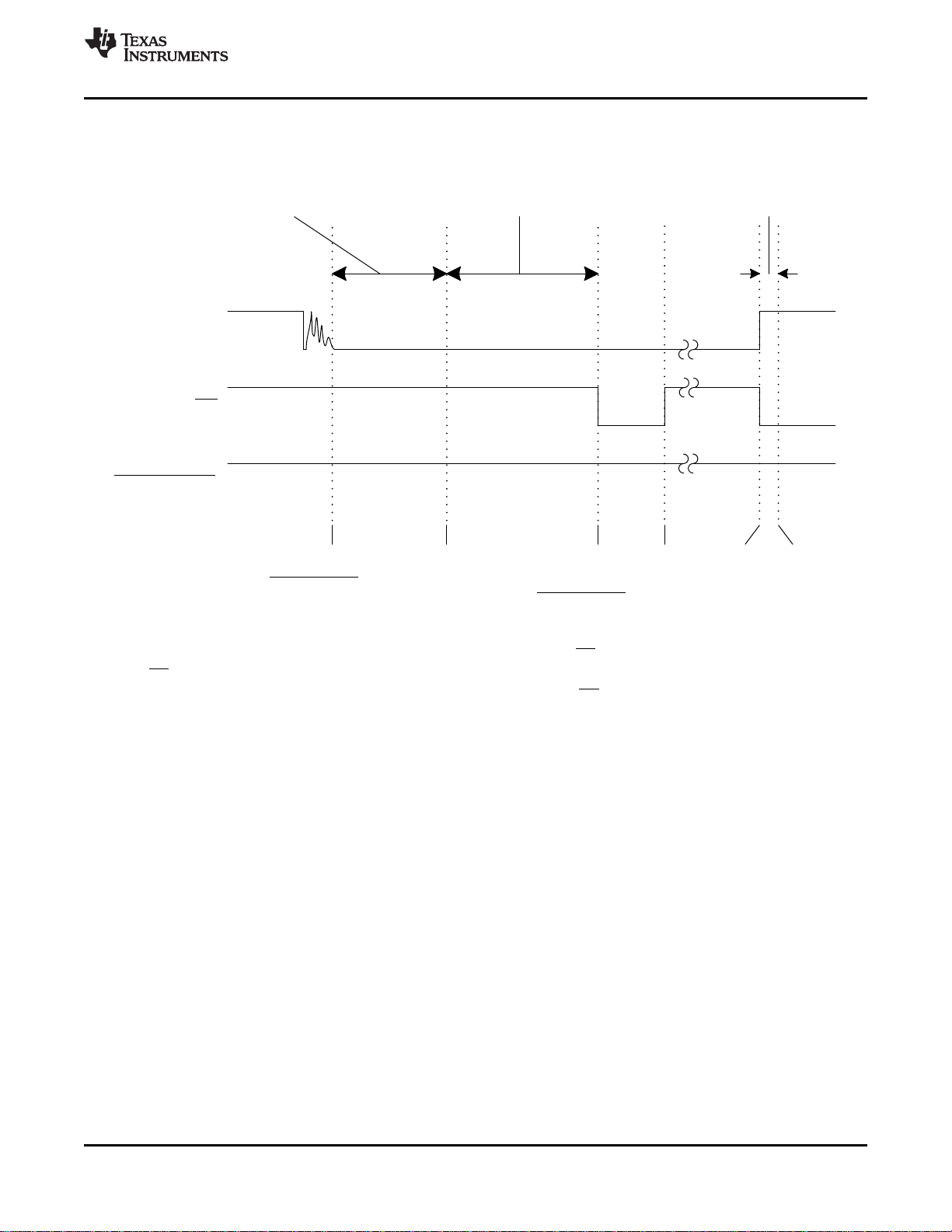
DET_TRIGGER
INT
Insertion
de-bounce time
(90 ms default )
Accessory detection time
(A) (B) (D) (E) (F)
Removal
wait time
MIC_PRESENT
High
(C)
www.ti.com
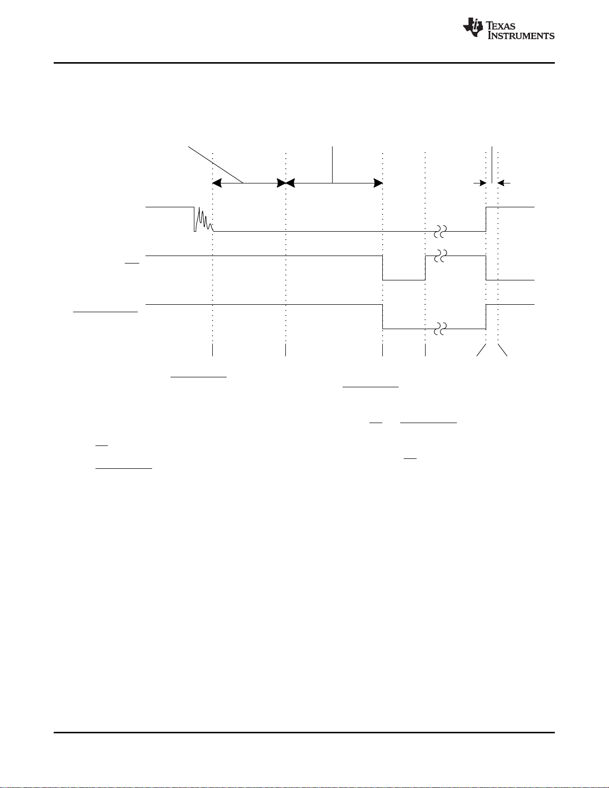
7.7 Timing Diagrams
TS3A227E
SCDS358B –NOVEMBER 2014–REVISED FEBRUARY 2015
A. (This is the point that DET_TRIGGER has stopped glitching and is fully low. The de-bounce time of 90 ms starts from
the point that the pin is constantly below the VILlevel. Any time the DET_TRIGGER pin cross the VIHlevel the de-
bounce timer will restart.
B. Point B is the end of the insertion de-bounce time and the beginning of accessory detection.
C. Detection has completed at this point. The switches will be routed before the INT pin is pulled low.
D. INT is cleared after the host reads the interrupt register.
E. The headset is removed here. The switch states will change immediately and INT will be pulled low.
F. After a 50 ms removal de-bounce timer the TS3A227E will go back into sleep mode if manual switch control is not
enabled
Figure 1. 3-Pole Accessory
Copyright © 2014–2015, Texas Instruments Incorporated Submit Documentation Feedback 9
Product Folder Links: TS3A227E
DET_TRIGGER
INT
Insertion
de-bounce time
(90 ms default )
Accessory detection time
(A) (B) (D) (E) (F)
Removal
wait time
MIC_PRESENT
High
(C)
TS3A227E
SCDS358B –NOVEMBER 2014–REVISED FEBRUARY 2015
Timing Diagrams (continued)
www.ti.com
A. This is the point that DET_TRIGGER has stopped glitching and is fully low. The de-bounce time of 90 ms starts from
the point that the pin is constantly below the VILlevel. Any time the DET_TRIGGER pin cross the VIH level the de-
bounce timer will restart.
B. Point B is the end of the insertion de-bounce time and the beginning of accessory detection.
C. Detection has completed at this point. The switches will be routed before the INT and MIC_PRESENT pins are pulled
low.
D. INT is cleared after the host reads the interrupt register.
E. The headset is removed here. The switch states will change immediately and INT will be pulled low. The
MIC_PRESENT pin will be released.
F. After a 50 ms removal de-bounce timer the TS3A227E will go back into sleep mode if manual switch control is not
enabled
Figure 2. 4-Pole Accessory
10 Submit Documentation Feedback Copyright © 2014–2015, Texas Instruments Incorporated
Product Folder Links: TS3A227E
DET_TRIGGER
INT
Insertion
de-bounce time
(90 ms default )
Accessory detection time
(A) (B) (C) (D) (E) ( F)
Removal
wait time
MIC_PRESENT
High
TS3A227E
www.ti.com
SCDS358B –NOVEMBER 2014–REVISED FEBRUARY 2015
Timing Diagrams (continued)
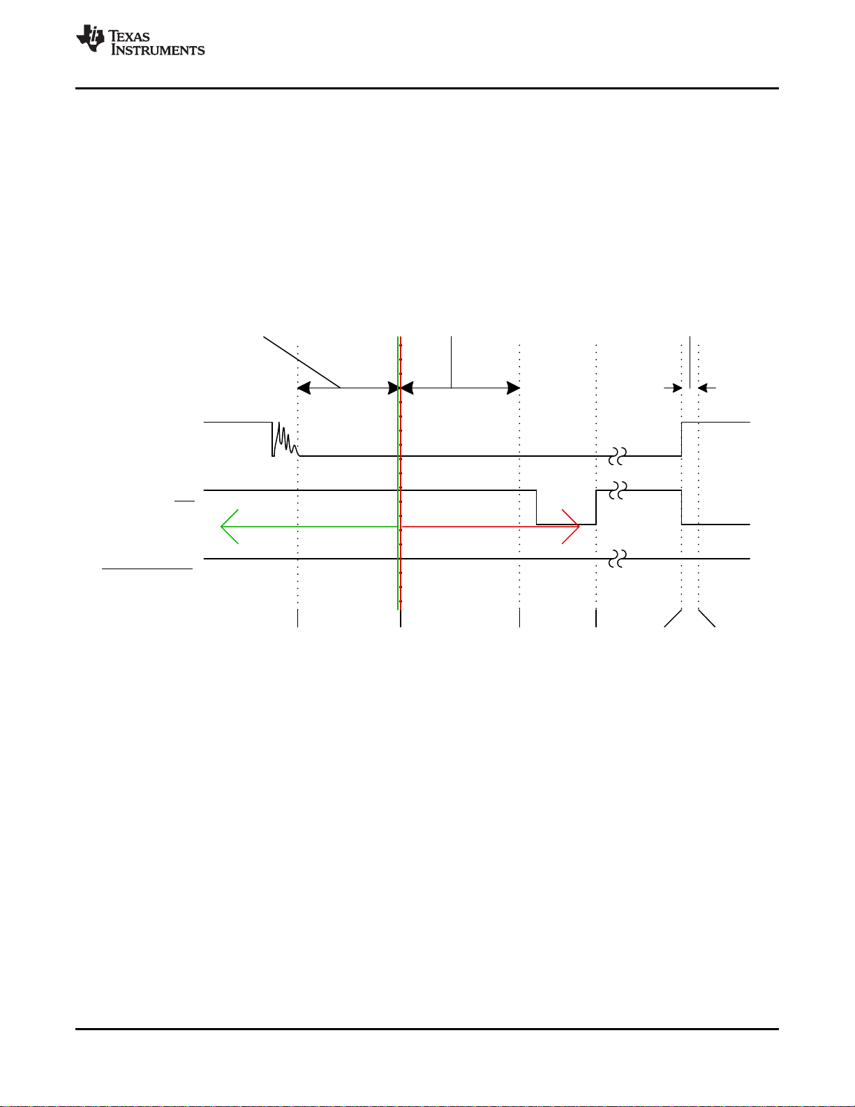
7.7.1 Removal
A removal event will interrupt any on-going process in the TS3A227E. The following diagram depicts how the
device “jumps” during a removal.
If the removal event occurs during the insertion de-bounce period the TS3A227E will jump to the (A) point of the
diagram depicted by the green arrow and line.
Any time after point (B) has been reached and the accessory is removed the device jumps to point (E), which
includes key press detection. Under Manual Switch Control the switch states will not change.
Copyright © 2014–2015, Texas Instruments Incorporated Submit Documentation Feedback 11
Figure 3. Removal Timing During Insertion
Product Folder Links: TS3A227E
I
GND
R2/SLV DFET
V
SLEEVE/RING2
Channel ON
RON= V
SLEEVE/RING2
/ I
GND
I
GNDA
R2/SLV GNDFET
V
SLEEVE/RING2
Channel ON
RON= V
SLEEVE/RING2
/ I
GNDA
Frequency (Hz)
THD (%)
10 2030 50 100 200 5001000 10000 100000
0
0.0005
0.001
0.0015
0.002
0.0025
0.003
0.0035
D001
200 mVpp
500 mVpp
TS3A227E
SCDS358B –NOVEMBER 2014–REVISED FEBRUARY 2015
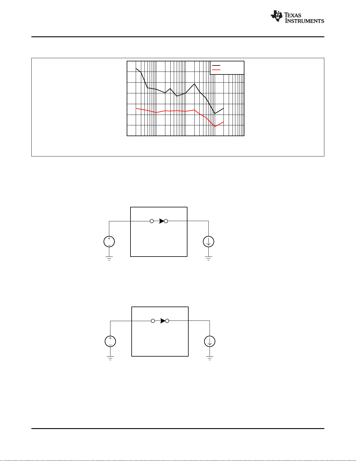
7.8 Typical Characteristics
8 Parameter Measurement Information
www.ti.com
Figure 4. S3PX THD
Figure 5. RING2/SLEEVE GNDFET On Resistance Measurement
Figure 6. RING2/SLEEVE DFET On Resistance Measurement
12 Submit Documentation Feedback Copyright © 2014–2015, Texas Instruments Incorporated
Product Folder Links: TS3A227E
V
OUT
Switch
V
IN
Channel OFF
I
RING 2_SENSE/SLEEVE_ SENSE
S3PS/R
S3GS/R
V
MICP/GND_SENSE
Channel ON
RON= V
MICP/GND_SENSE
/ I
RING2_SENSE /SLEEVE_SENSE
I
GND
S1/S2
V
MICP/GND_SENSE
Channel ON
RON= V
MICP/GND_SENSE
/ I
GND
www.ti.com
TS3A227E
SCDS358B –NOVEMBER 2014–REVISED FEBRUARY 2015
Parameter Measurement Information (continued)
Figure 7. S1/S2 On Resistance Measurement
Figure 8. S3PS, S3PR, S3GS, S3GR On Resistance Measurement
Figure 9. Switch Off Leakage Current
Copyright © 2014–2015, Texas Instruments Incorporated Submit Documentation Feedback 13
Product Folder Links: TS3A227E
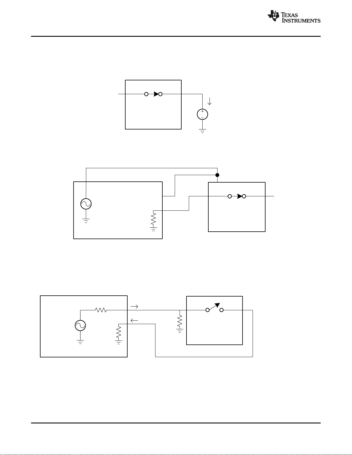
Switch
Network Analyzer
Source
Signal
50 Ω
50 Ω
Channel Off
V
MICP/GND_SENSE
V
SLEEVE_SENSE/RING2 _SENSE
50 Ω
Switch
Channel ON
V
DD
3.3 V ± 200 mV
PP
Reference
Test
Source Generator
Source
Signal
50 Ω
V
OUT
Switch
Channel ON
I
Leakage
TS3A227E
SCDS358B –NOVEMBER 2014–REVISED FEBRUARY 2015
Parameter Measurement Information (continued)
Figure 10. Switch On Leakage Current
www.ti.com
Figure 11. Power Supply Rejection Ratio (PSRR)
Figure 12. Switch Off Isolation
14 Submit Documentation Feedback Copyright © 2014–2015, Texas Instruments Incorporated
Product Folder Links: TS3A227E
Audio Analyzer
Source
Signal
600 Ω
600 Ω
V
MICP
V
SLEEVE_SENSE/RING2_SENSE
Switch
Network Analyzer
Source
Signal
50 Ω
50 Ω
V
MICP
V
SLEEVE_SENSE
50 Ω
50 Ω
V
GND_SENSE V
RING2_SENSE
Switches
www.ti.com
TS3A227E
SCDS358B –NOVEMBER 2014–REVISED FEBRUARY 2015
Parameter Measurement Information (continued)
Figure 13. Channel Separation
Figure 14. Total Harmonic Distortion (THD) and SNR
Copyright © 2014–2015, Texas Instruments Incorporated Submit Documentation Feedback 15
Product Folder Links: TS3A227E
Digital
Core
SDA
SCL
R
PU
C
L
V
PU
V
TEST
V
TEST
SCL
V
TEST
70
%
30
%
t
OFF
t
ON
V
TEST
SCL
V
TEST
90
%
10
%
t
ON
t
OFF
V
MICP/GND _SENSE
Digital
Core
SDA
SCL
R
L
C
L
V
TEST
TS3A227E
SCDS358B –NOVEMBER 2014–REVISED FEBRUARY 2015
Parameter Measurement Information (continued)
www.ti.com
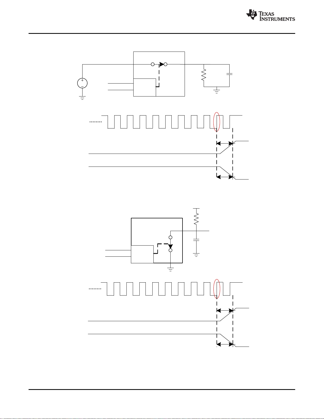
Figure 15. S3 t
N
OFF/tO
Figure 16. S1, S2, GNDFET and DFET tON/t
16 Submit Documentation Feedback Copyright © 2014–2015, Texas Instruments Incorporated
Product Folder Links: TS3A227E
OFF

TS3A227E
www.ti.com
SCDS358B –NOVEMBER 2014–REVISED FEBRUARY 2015
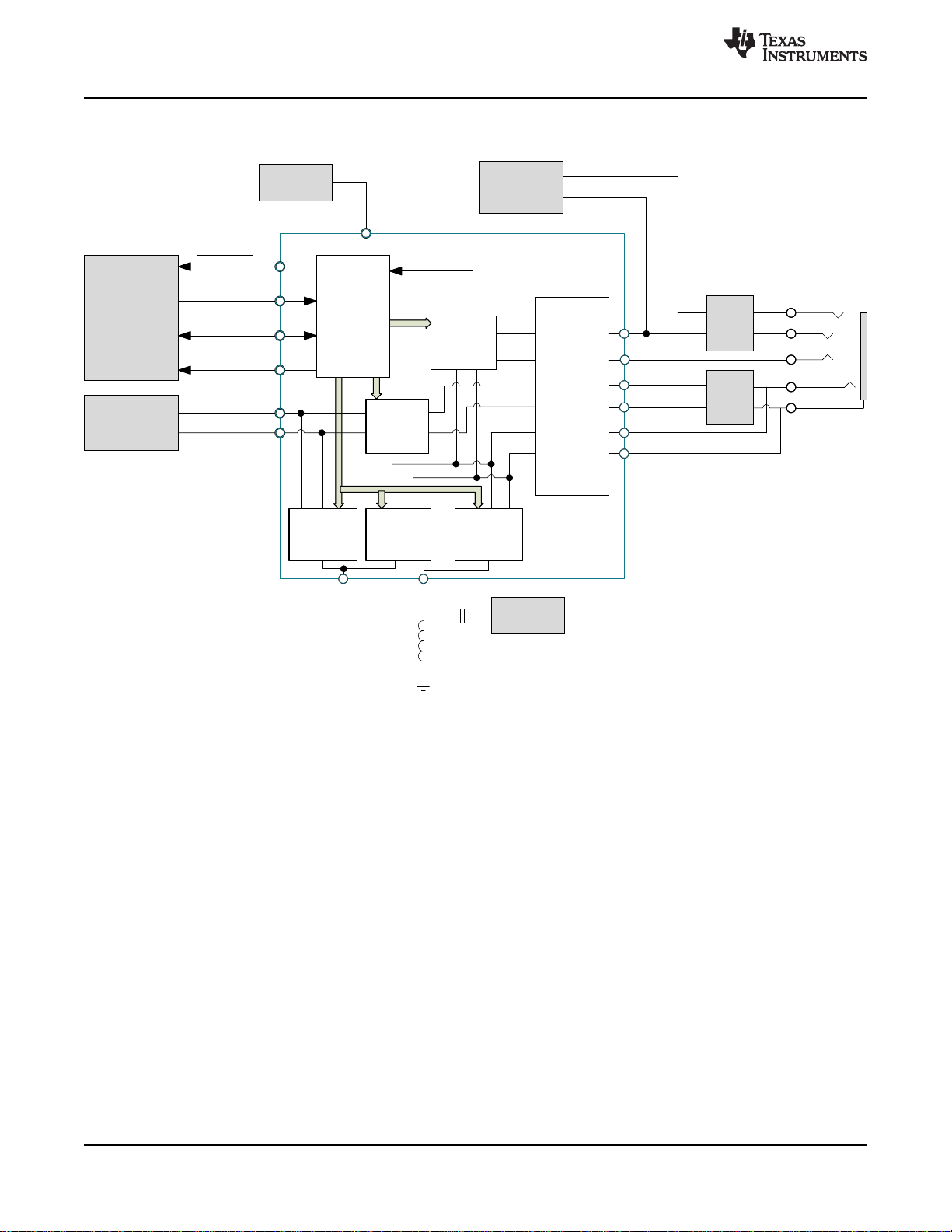
9 Detailed Description
9.1 Overview
The TS3A227E is an autonomous audio accessory switch with adjustable de-bounce settings, ultra-low RON
ground FETs, depletion FETs and manual I2C control.
The detection sequence is initiated via the external DET_TRIGGER pin or via I2C command. The device
incorporates internal de-bounce timings that remove the need for external RC circuits, reducing cost and overall
PCB footprint. Additionally all switches of the TS3A227E and the internal de-bounce timings can be controlled
through I2C.
Before an insertion, TS3A227E isolates the MICBIAS voltage output from the audio jack to remove click/pop
noise that can be created during an insertion event. In addition the device also includes depletion FETs to
ground the accessory SLEEVE and RING2 pins when VDD is not powered. This removes the humming noise
that can be created when plugging an accessory into and unpowered system.
The TS3A227E detects the presence and configuration of the microphone in an attached headset upon insertion.
Upon detection of a microphone the TS3A227E automatically connects a system analog microphone pin (MICP)
to the appropriate audio jack connection. The device also automatically routes the device GNDA pin to the
headset ground. After a 4-pole headset insertion the host can enable the Key Press detection feature of the
TS3A227E.
The device also features an ultra-low power sleep mode to conserve battery life when an accessory is not
inserted.
For FM transmission the ground FETs of the device can be used as an FM transmission path by placing the FM
receiver and matching network on the GNDA pin. The FM support bit must be set to ‘1’ through I2C for FM
transmission to pass.
Copyright © 2014–2015, Texas Instruments Incorporated Submit Documentation Feedback 17
Product Folder Links: TS3A227E
BATTERY
DIGITAL BASEBAND
MIC_PRESENT
SCL
SDA
INTB
VDD
MICROPHONE
AMPLIFIER
EMI
FILTER
EMI
FILTER
RING2_SENSE
SLEEVE_SENSE
TIP
DET_TRIGGER
RING2
SLEEVE
MICP
GND_SENSE
AUDIO
AMPLIFIER
Mic Switch
Matrix
ESD Protection
Depletion FETs
GND Switch
Matrix
TS3A227 E
Detection
Circuitry
Digital interface
control
GND GNDA
FM
Receiver
S1 and S2
TS3A227E
SCDS358B –NOVEMBER 2014–REVISED FEBRUARY 2015
9.2 Functional Block Diagram
www.ti.com
18 Submit Documentation Feedback Copyright © 2014–2015, Texas Instruments Incorporated
Product Folder Links: TS3A227E
R M GL
16-2 kΩ
16- 2 kΩ
600-4kΩ
OMTP
4-pole TRRS
Tip Ring1 SleeveRing2
R G ML
16-2 kΩ
16- 2 kΩ
600-4kΩ
Standard
Tip Ring Sleeve
3-pole TRS
R GL
16-2 kΩ
16- 2 kΩ
TRS
TS3A227E
www.ti.com
SCDS358B –NOVEMBER 2014–REVISED FEBRUARY 2015
9.3 Feature Description
9.3.1 Accessory Configuration Detection
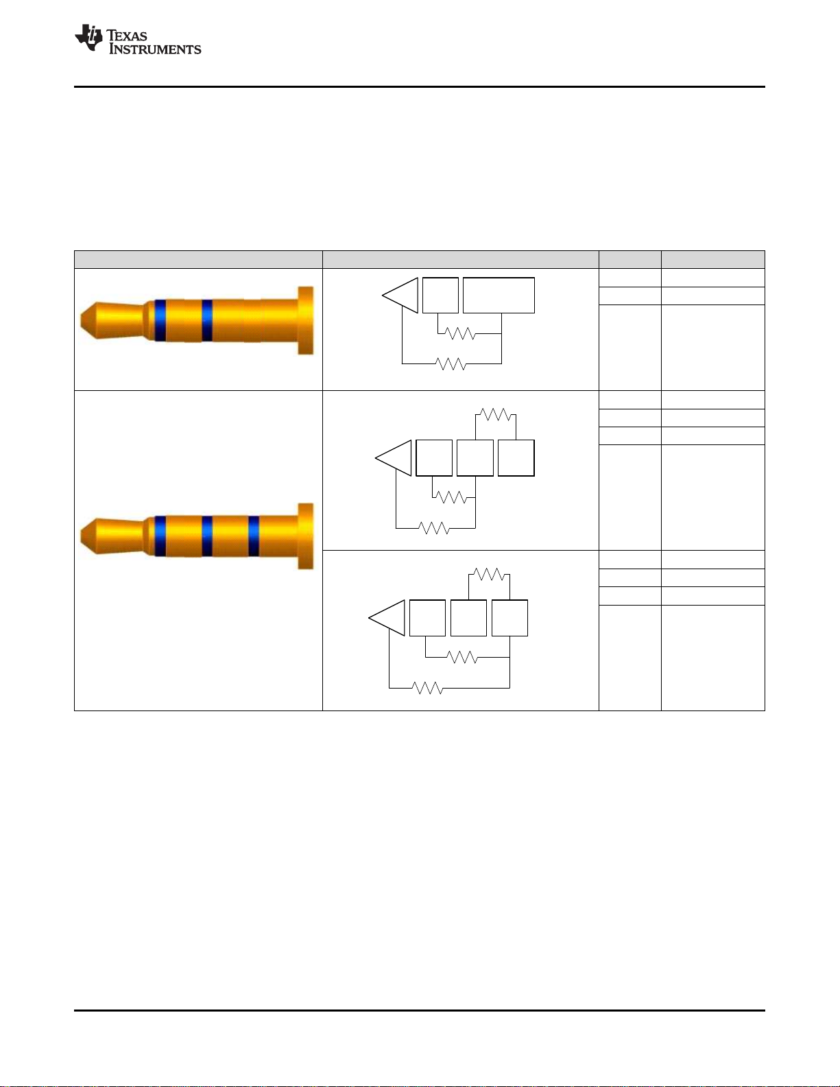
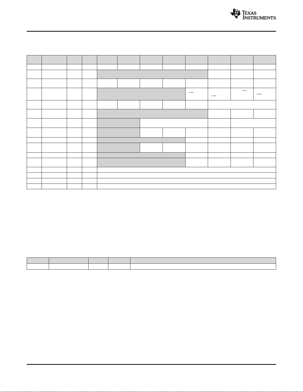
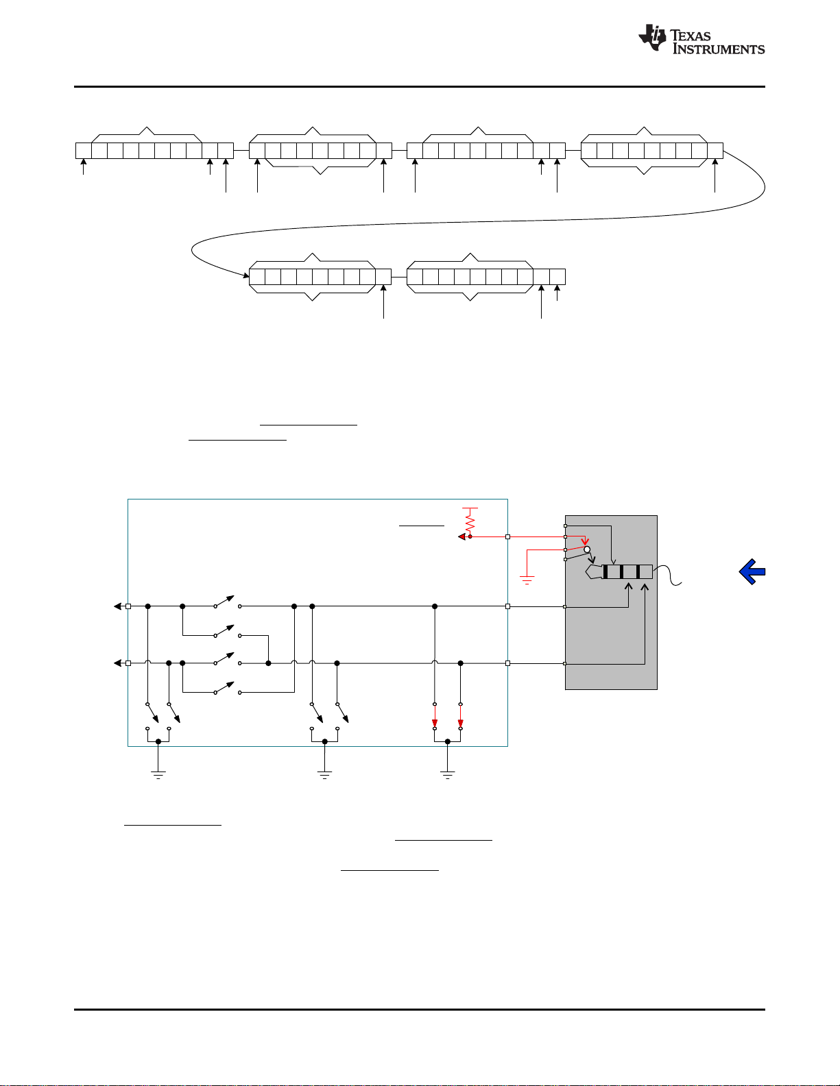
There are currently two difference configurations for headsets with microphones as shown in Table 1. Many
codecs requires that the system designer make a tough decision via a hardware connection which headset they
would like to support. This is done by directly connecting the microphone bias and the ground connections to the
sleeve and ring2 pins of the audio jack. For the end user this leaves a headset standard as fully unsupported.
Table 1. Two Difference Configurations for Headsets
PHYSICAL CONNECTOR INTERNAL IMPEDANCE NETWORK PIN NAME CONFIGURATION
Tip Audio Left
Ring Audio Right
Sleeve Ground
Tip Audio Left
Ring1 Audio Right
Ring2 Ground
Sleeve Microphone
Tip Audio Left
Ring1 Audio Right
Ring2 Microphone
Sleeve Ground
The TS3A227E fills this system gap by detecting the presence and location of the microphone and automatically
routing the MICBIAS and ground lines to support each headset. This enhances the overall user experience by
allowing headsets from all manufacturers.
9.3.2 Optional Manual I2C Control
The TS3227E also features optional manual I2C control for enhanced system flexibility. This allows the system
designer to manually control the switches and de-bounce settings at their discretion enabling the TS3A227E to
adapt to unique use cases.
This is an optional feature that does not need to be used for the device to operate autonomously.
9.3.3 Adjustable De-bounce Timings
The TS3A227E features manual control of the insertion de-bounce timer with selectable values. The default
insertion de-bounce timer is 90 ms.
This eliminates the need for external RC components which reduces BOM cost, the PCB footprint of the external
RC components. Further information on how to select an appropriate de-bounce timer can be found in the
application and implementation section.
Copyright © 2014–2015, Texas Instruments Incorporated Submit Documentation Feedback 19
Product Folder Links: TS3A227E

TS3A227E
SCDS358B –NOVEMBER 2014–REVISED FEBRUARY 2015
www.ti.com
9.3.4 Key Press Detection
After a headset is inserted, the host can enable Key Press detection through the I2C registers. This will configure
the TS3A227E to detect up to 4 different keys and report when the key is pressed and released.
9.3.5 Click Pop Noise Reduction
During an accessory insertion and removal event the TS3A227E use special techniques to remove the click/pop
noise that can occur with a traditional implementation creating a better user experience.
9.3.6 Power off Noise Removal
In a system that intends to support both headset types, the end user can place the system into sleep mode and
leave a headset/speaker plugged into the audio jack. If the audio jack switch is turned off to conserve power in
the sleep mode this would typically mean the headset/speaker ground would not be connected because there is
no power to turn on the ground FETs. This creates an audible humming noise at the speaker/headset output that
can be discomforting to listen to.
By utilizing always on depletion FETs this issue can be removed and the headset/speaker can be connected to
ground even with the device unpowered.
9.3.7 Sleep Mode
The TS3A227E will automatically enter a low power sleep when no accessory is inserted and manual switch
control is not enabled. After an accessory is inserted the device will wake, run detection, and configure the
switches as necessary.
9.3.8 Codec Sense Line
In the complex systems of today, there is an increasing amount of ICs on any given board. The issue this creates
is that a codec can be far away from the audio jack and there is a potential difference between the grounding of
the codec and the grounding of the headset.
By incorporating a ground sense line into the TS3A227E the codec can compensate for this offset and create a
higher quality audio experience.
9.3.9 FM Support
FM can be picked up using the headset ground line and passed through the ground FETs of the TS3A227E. By
having a bandwidth of 200 MHz the full FM band can be passed through these FETs to a FM matching network
and the FM receiver.
9.4 Device Functional Modes
9.4.1 Sleep Mode
The device will realize a sleep mode of 1 µA if the following are true:
• No accessory is inserted
• Manual Switch Control = ‘0’
The TS3A227E will respond to I2C communication and insertion events while in sleep mode. The user can set
the de-bounce settings and device configuration as desired while in the sleep mode. If the user sets the Manual
Switch Control bit to ‘1’ the device will turn on all blocks and come out of sleep mode.
If there is no accessory inserted and the users exits manual switch control, the switches will revert to the noinsertion state and all unnecessary blocks of the TS3A227E will turn off and enter the sleep mode.
20 Submit Documentation Feedback Copyright © 2014–2015, Texas Instruments Incorporated
Product Folder Links: TS3A227E

TS3A227E
www.ti.com
SCDS358B –NOVEMBER 2014–REVISED FEBRUARY 2015
Device Functional Modes (continued)
9.4.2 Manual Switch Control
The TS3A227E supports manual switch control that can be utilized by setting Bit6 of the Device Settings 1
register to ‘1’.
Key operational characteristics of manual switch control are below.
1. Enabling the manual switch control does not disable automatic insertion and accessory type detection.
2. Manual Switch Control is blocked during accessory type detection which includes an automatic detection
sequence or a manual SW triggered detection sequence. Any changes to the switch control registers, or
setting the device to manual switch control will not update the switches until after the accessory type
detection has completed.
3. Manual Switch Control is also blocked during de-bounce periods.
4. Excluding items 2 and 3 above, immediately after the system enables manual switch control the switch states
will change to reflect the switch control registers. It is advised to set the desired state of the switches before
enabling manual switch control.
5. Turning off the depletion FETs of the device will result in increased power consumption as defined in the
electrical characteristics table.
6. Immediately upon setting Manual Switch Control = ‘0’ the device will automatically configure the switches to
the latest detection state. If an accessory is inserted but the TS3A227E has not run detection due to
Auto_Det_EN = ‘0’, the switch status will revert to the no insertion state.
7. The device cannot be in sleep mode and utilize manual switch control at the same time.
9.4.3 Manual Switch Control Use Cases
The table below captures what occurs after a 3-pole insertion with the Manual Switch Control, Auto DET Enable,
and DET Trigger bits set to the following before an insertion.
MANUAL DOES TYPE
SWITCH DETECTION
CONTROL RUN
0 0 0 no No-insertion 0
0 0 1 yes 3-pole config 0
0 1 0 yes 3-pole config 0
0 1 1 yes 3-pole config 0
1 0 0 no Switch control registers 0
1 0 1 yes Switch control registers 0
1 1 0 yes Switch control registers 0
1 1 1 yes Switch control registers 0
AUTO DET DET TRIGGER SWITCH STATUS AFTER DET TRIGGER (SW) AFTER
EN (SW) INSERTION INSERTION
The table below captures the switch and relevant register outputs for sequence 1.
EVENT 3-POLE 4-POLE
NO. BIT OMTP BIT
1 Device powers up No-insertion 0 0 0
2 User sets Auto DET Enable = ‘0’ No-insertion 0 0 0
3 3-pole accessory is inserted No-insertion 0 0 0
4 System sets Manual Switch Control = ‘1’ System controlled 0 0 0
5 System sets switch control registers = 0xFF System controlled 0 0 0
6 System sets Manual Switch Control = ‘0’ No-insertion 0 0 0
EVENT DESCRIPTION SWITCH STATUS
4-POLE
STANDARD BIT
Copyright © 2014–2015, Texas Instruments Incorporated Submit Documentation Feedback 21
Product Folder Links: TS3A227E

TS3A227E
SCDS358B –NOVEMBER 2014–REVISED FEBRUARY 2015
www.ti.com
In sequence 1 at event 3 the switch status does not change because the system set the Auto DET Enable = ‘0’.
When the accessory is inserted we will not run detection and not change the switches because of this.
At event 6 the system turns off manual switch control, the switch state reverts back to the No-insertion state
because the TS3A227E has not ran detection.
The table below captures the switch and relevant register outputs for sequence 2.
EVENT SWITCH STATUS 3-POLE 4-POLE 4-POLE
NO. AFTER EVENT BIT STANDARD BIT OMTP BIT
1 Device powers up No-insertion 0 0 0
2 User sets Auto DET Enable = ‘0’ No-insertion 0 0 0
3 3-pole accessory is inserted No-insertion 0 0 0
4 System sets Manual Switch Control = ‘1’ System controlled 0 0 0
5 System sets switch control registers = 0xFF System controlled 0 0 0
6 System sets DET Trigger = ‘1’ System controlled 1 0 0
7 System sets Manual Switch Control = '0' 3-pole configuration 1 0 0
EVENT DESCRIPTION
In sequence 2 at event 3 the switch status does not change because the system set the Auto DET Enable = ‘0’.
When the accessory is inserted we will not run detection and not change the switches because of this.
At event 6 the system turns triggers a manual type detection and the TS3A227E detects a 3-pole accessory. The
switch state will remain in the system controlled state.
At event 7 the system exits manual switch control. The switch status will then change back to the last detection
state. Because detection was ran at event 6 and a 3-pole was detected, the switch state will reflect that of the 3pole switch configuration.
22 Submit Documentation Feedback Copyright © 2014–2015, Texas Instruments Incorporated
Product Folder Links: TS3A227E

TS3 A227E
MICP
GND_SENSE
S3PR
SLEEVE
S3PS
S3GS
S3GR
S1 S 2
RING2
GNDFET
SLEEVE
GNDFET
RING2
DFET
SLEEVE
DFET
RING2
SLEEVE_SENSE
RING 2_SENSE
GND GNDGNDA
Audio Jack
L R G M
FM
Receiver
TS3A227E
www.ti.com
SCDS358B –NOVEMBER 2014–REVISED FEBRUARY 2015
9.4.4 FM Support Mode
FM support mode needs to be entered via I2C through the Device Settings register. This will turn off the
depletion switches when an accessory is inserted, eliminating the extra ground path. The ground line of the
headset/headphone is used for FM transmission. This signal must pass through the TS3A227E ground FETs as
shown in Figure 17 where the red line indicates the transmission path.
Figure 17. FM Support Transmission Path
NOTE
FM support should be enabled before an accessory is inserted. Toggling the FM
support bit after a headset is inserted can cause a pop noise to be heard by the end
user.
Copyright © 2014–2015, Texas Instruments Incorporated Submit Documentation Feedback 23
Product Folder Links: TS3A227E
TS3A227E
SCDS358B –NOVEMBER 2014–REVISED FEBRUARY 2015
9.5 Register Maps
The I2C address of the TS3A227E is b’0111011X or 77h read and 76h write.
www.ti.com
Addr
(xxh)
00h Device ID R 11h 0 0 0 1 0 0 0 1
01h Interrupt R 00h Reserved DC Ins/Rem Event
02h R 00h Key 4 Press Key 3 Release Key 3 Press Key 2 Release Key 2 Press Key 1 Release Key 1 Press
03h Interrupt Disable R/W 08h Reserved INT Disable Conversion
04h Device Settings R/W 23h Reset DET Trigger FM Support Insertion De-bounce Time
05h Device Setting 1 R/W 00h Reserved Raw Data En ADC Trigger
06h Device Setting 2 R/W 0Eh Reserved MICBIAS Setting Key Press De-bounce
07h Switch Control 1 R/W 00h Reserved RING2 DFET Switch 2 Switch 1
08h Switch Control 2 R/W 00h Reserved S3PS S3PR S3GS S3GR
09h Switch Status 1 R 0Ch Reserved RING2DFET Switch 2 Switch 1
0Ah Switch Status 2 R 00h Reserved S3PS S3PR S3GS S3GR
0Bh R 00h Reserved 4-pole OMTP 3-pole
0Ch ADC Output R 00h ADC
0Dh Threshold 1 R/W 20h KP Threshold 1
0Eh Threshold 2 R/W 40h KP Threshold 2
0Fh Threshold 3 R/W 68h KP Threshold 3
Name Type Reset Bit7 Bit6 Bit5 Bit4 Bit3 Bit2 Bit1 Bit0
ADC
Conversion
Key Press Key 4
Interrupts Release
ADC
INT Disable
Manual Switch Auto DET
Control Enable
Key Press
Enable
Key Release
De-bounce
SLEEVE SLEEVE
GNDFET DFET
SLEEVE SLEEVE
GNDFET DFET
Accessory Insertion 4-Pole
Status Status Standard
RING2
GNDFET
RING2
GNDFET
DC INT Ins/Rem Event
Disable INT Disable
Interrupt and Key Press Interrupt register notes:
• The device will continue to automatically run type detection and key press detection even if the host has not
serviced the interrupts.
• Consecutive reads of an interrupt register at 400 kHz will not allow time for the internal registers to clear and
will appear. The internal digital core requires 200 µs to clear the register after it has been read.
9.6 Register Field Descriptions
9.6.1 Device ID Register Field Descriptions (Address 00h)
Figure 18. Device ID Register Field Descriptions (Address 00h)
Bit Field Type Reset Description
7-0 Device ID R 11h Unique Revision number
24 Submit Documentation Feedback Copyright © 2014–2015, Texas Instruments Incorporated
Product Folder Links: TS3A227E

www.ti.com
SCDS358B –NOVEMBER 2014–REVISED FEBRUARY 2015
9.6.2 Interrupt Register Field Descriptions (Address 01h)
Table 2. Interrupt Register Field Descriptions (Address 01h)
Bit Field Type Reset Description
7-3 Reserved R 0h
2 ADC Conversion R 0h ADC Conversion complete Interrupt. Flagged after a manual ADC conversion is
1 DC R 0h Detection Complete interrupt. Flagged after detection is completed for an
0 Ins/Rem Event R 0h Insertion or removal interrupt indicator. This bit is set if there is an insertion or
complete.
Interrupt bit is cleared after being read through I2C or after a removal event.
0h = Default state
1h = ADC Conversion Complete
insertion sequence. This bit is also flagged after completion of a manually
triggered detection.
Interrupt bit is cleared after being read through I2C or after a removal event.
0h = Default state
1h = Detection Completed
removal event. The Insertion status bit of the Accessory Status register (0Bh)
must be checked if this bit is set.
Interrupt bit is cleared after being read through I2C
0h = Default state
1h = Accessory has been inserted or removed
TS3A227E
9.6.3 Key Press Interrupt Register Field Descriptions (Address 02h)
Table 3. Key Press Interrupt Register Field Descriptions (Address 02h)
Bit Field Type Reset Description
7 Key 4 Release R 0h This interrupt bit is set after the user has released key 4 on the accessory for a
6 Key 4 Press R 0h This interrupt bit is set after the user has pressed key 4 on the accessory for a
5 Key 3 Release R 0h This interrupt bit is set after the user has pressed Key 3 on the accessory for a
duration longer than the Key Release De-bounce timer.
This bit will auto-clear on the following conditions:
● Host reads the register through I2C
● The KP Enable bit is set to ‘0’
— The KP Enable bit is set to ‘0’ automatically after a removal
● The Key 4 press bit is set ot '1'
0h = Default State
1h = Key 4 was released
duration longer than the Key Press De-bounce timer.
This bit will auto-clear on the following conditions:
● Host reads the register through I2C
● The KP Enable bit is set to ‘0’
— The KP Enable bit is set to ‘0’ automatically after a removal
0h = Default State
1h = Key 4 was released
duration longer than the Key Release De-bounce timer.
This bit will auto-clear on the following conditions:
● Host reads the register through I2C
● The KP Enable bit is set to ‘0’
— The KP Enable bit is set to ‘0’ automatically after a removal
● The Key 3 Press bit is set to ‘1’
0h = Default State
1h = Key 3 was released
Copyright © 2014–2015, Texas Instruments Incorporated Submit Documentation Feedback 25
Product Folder Links: TS3A227E

TS3A227E
SCDS358B –NOVEMBER 2014–REVISED FEBRUARY 2015
Table 3. Key Press Interrupt Register Field Descriptions (Address 02h) (continued)
Bit Field Type Reset Description
4 Key 3 Press R 0h This interrupt bit is set after the user has pressed Key 3 on the accessory for a
duration longer than the Key Press De-bounce timer.
This bit will auto-clear on the following conditions:
● Host reads the register through I2C
● The KP Enable bit is set to ‘0’
— The KP Enable bit is set to ‘0’ automatically after a removal
0h = Default State
1h = Key 3 was released
3 Key 2 Release R 0h This interrupt bit is set after the user has pressed Key 2 on the accessory for a
duration longer than the Key Release De-bounce timer.
This bit will auto-clear on the following conditions:
● Host reads the register through I2C
● The KP Enable bit is set to ‘0’
— The KP Enable bit is set to ‘0’ automatically after a removal
● The Key 2 Press bit is set to ‘1’
0h = Default State
1h = Key 2 was released
2 Key 2 Press R 0h This interrupt bit is set after the user has pressed Key 2 on the accessory for a
duration longer than the Key Press De-bounce timer.
This bit will auto-clear on the following conditions:
● Host reads the register through I2C
● The KP Enable bit is set to ‘0’
— The KP Enable bit is set to ‘0’ automatically after a removal
0h = Default State
1h = Key 2 was released
1 Key 1 Release R 0h This interrupt bit is set after the user has pressed Key 1 on the accessory for a
duration longer than the Key Release De-bounce timer. This bit is used for raw
data release events.
This bit will auto-clear on the following conditions:
● Host reads the register through I2C
● The KP Enable bit is set to ‘0’
— The KP Enable bit is set to ‘0’ automatically after a removal
● The Key 1 Press bit is set to ‘1’
0h = Default State
1h = Key 1 was released
0 Key 1 Press R 0h This interrupt bit is set after the user has pressed Key 1 on the accessory for a
duration longer than the Key Press De-bounce timer. This bit is used for raw data
press events.
This bit will auto-clear on the following conditions:
● Host reads the register through I2C
● The KP Enable bit is set to ‘0’
— The KP Enable bit is set to ‘0’ automatically after a removal
0h = Default State
1h = Key 1 was released
www.ti.com
26 Submit Documentation Feedback Copyright © 2014–2015, Texas Instruments Incorporated
Product Folder Links: TS3A227E

www.ti.com
SCDS358B –NOVEMBER 2014–REVISED FEBRUARY 2015
9.6.4 Interrupt Disable Register Field Descriptions (Address 03h)
Table 4. Interrupt Disable Register Field Descriptions (Address 03h)
Bit Field Type Reset Description
7-3 Reserved R 0h
+3 INT Disable R/W 1h Enables or disables all interrupts. Disabling the interrupts will cause the INT to
2 ADC Conversion R/W 0h Enables or disables the ADC conversion interrupt. Disabling the interrupt will
INT Disable cause INT to not assert but the interrupt bit will still be set .
1 DC INT Disable R/W 0h Enables or disables the DC interrupt. Disabling the interrupt will cause INT to
0 Ins/Rem Event INT R/W 0h Enables or disables the Ins/Rem Event interrupt. Disabling the interrupt will
Disable cause INT to not assert but the interrupt bit will still be set.
not assert but the bits will still populate.
0h = interrupts are enabled
1h = interrupts are disabled
In the use case that this bit is == ‘1’ and a key is pressed, the Key Press
interrupt will still assert the INT pin. If the host issues a software ADC trigger
after the key has been pressed, the interrupt will not assert as that ADC
conversion is the only interrupt present.
0h = ADC Conversion interrupt is enabled
1h = ADC Conversion interrupt is disabled
not assert but the interrupt bit will still be set.
0h = DC interrupt is enabled
1h = DC interrupt is disabled
0h = Ins/Rem Event interrupt is enabled
1h = Ins/Rem Event interrupt is disabled
TS3A227E
9.6.5 Device Settings Field Descriptions (Address 04h)
Table 5. Device Settings Field Descriptions (Address 04h)
Bit Field Type Reset Description
7 Reset R/W 0h Initiates software reset of the TS3A227E. This will interrupt any on-going
6 Manual Switch R/W 0h Enables Manual control of the TS3A227E switches. After enabling manual switch
Control control the switch status will immediately reflect the values in the switch control
5 Auto DET Enable R/W 1h Controls whether detection is automatically ran after an insertion.
4 DET Trigger R/W 0h Manually triggers detection. This bit is auto cleared after detection is completed.
3 FM Support R/W 0h Turns on FM support. This will turn off the depletion FETs if any accessory is
operation internal to the device.
0h = Default state
1h = Initiates a reset
registers provided accessory type.
0h = Manual switch control disabled
1h = Manual switch control enabled
0h = Auto accessory detection is disabled
1h = Auto accessory detection is enabled
A DET Trigger request will be ignored in the following cases:
● A detection event is currently being service.
● The interrupt register is not cleared (Register 02h must be = 00h)
● There is no accessory inserted (/DET_TRIGGER is high)
0h = Default value
1h = Manually trigger detection
inserted allowing FM transmission through the ground FETs at the cost of
increased current consumption.
0h = FM not supported and depletion FETs are on after an insertion
1h = FM supported and depletion FETs are off after an insertion
Copyright © 2014–2015, Texas Instruments Incorporated Submit Documentation Feedback 27
Product Folder Links: TS3A227E

TS3A227E
SCDS358B –NOVEMBER 2014–REVISED FEBRUARY 2015
www.ti.com
Table 5. Device Settings Field Descriptions (Address 04h) (continued)
Bit Field Type Reset Description
2.0 Insertion De-bounce R/W 3h Controls the insertion de-bounce timer. Values below are typical values that have
Time ±30% variation. Values in addition have a ±1 ms variation though this will only
really affect the 2 ms timer.
0h = 2 ms
1h = 30 ms
2h = 60 ms
3h = 90 ms
4h = 120 ms
5h = 150 ms
6h = 1 s
7h = 2 s
9.6.6 Key Press Settings 1 Field Descriptions (Address 05h) Table 6. Device Settings 1 Field Descriptions (Address 05h)
Bit Field Type Reset Description
7-3 Reserved R 0h
2 Key Press Enable R/W 0h Enables the Key Press detection of the TSA227E. This bit auto clears after a
1 Raw Data En R/W 0h Enables the Raw data mode for Key Press Detection. This bit auto clears if the
0 ADC Trigger R/W 0h Causes a manual ADC trigger if the Key Press Enable and Raw Data EN bits are
removal event.
If the Key Press Enable bit is set ‘1’ and the Manual Switch Control bit is set to
‘1’, the S3 matrix must be in one of the two correct position as described in the
Key Press Detection section for the TS3A227E to run key press detection.
0h = Default state
1h = Enables Key Press detection
Key Press Enable bit is set to ‘0’.
Enabling raw data mode will not clear the KP interrupt register. After enabling
Raw Data any key press and release event is recorded using the Key 1 Press
and Key 2 Press Release event. The ADC conversion will be recorded in the
ADC output register.
0h = Raw Data is not enabled
1h = Raw Data is enabled
both set to ‘1’. After the ADC conversion is complete the ADC Conversion
interrupt will be set and the ADC Output register will be populated.
This bit auto clears after the ADC Conversion is complete. A new ADC
Conversion can be initiated even if the ADC Conversion interrupt has not been
serviced.
0h = Default State
1h = Triggers ADC conversion
28 Submit Documentation Feedback Copyright © 2014–2015, Texas Instruments Incorporated
Product Folder Links: TS3A227E
www.ti.com
SCDS358B –NOVEMBER 2014–REVISED FEBRUARY 2015
9.6.7 Key Press Settings 2 Field Descriptions (Address 06h) Table 7. Device Settings 2 Field Descriptions (Address 06h)
Bit Field Type Reset Description
7-6 Reserved R 0h
5-3 MICBIAS Setting R/W 1h This controls the key press threshold. Set this setting closest to the intended
2 Key Release De- R/W 1h Controls the Key-Release de-bounce timer. Values below are typical values that
bounce have ±30% variation. Values in addition have a ±1 ms variation though this will
1-0 Key Press De- R/W 2h Controls the key press de-bounce timer. Values below are typical values that
bounce have ±30% variation. Values in addition have a ±1 ms variation though this will
MICBIAS voltage
0h = 2.1 V
1h = 2.2 V (Default)
2h = 2.3 V
3h = 2.4 V
4h = 2.5 V
5h = 2.6 V
6h = 2.7 V
7h = 2.8 V
only really affect the 2 ms timer.
0h = 2 ms
1h = 20 ms (Default)
only really affect the 2 ms timer.
0h = 2 ms
1h = 40 ms
2h = 80 ms (Default)
3h = 120 ms
TS3A227E
Copyright © 2014–2015, Texas Instruments Incorporated Submit Documentation Feedback 29
Product Folder Links: TS3A227E
TS3A227E
SCDS358B –NOVEMBER 2014–REVISED FEBRUARY 2015
9.6.8 Switch Control 1 Field Descriptions (Address 07h)
Table 8. Switch Control 1 Field Descriptions (Address 07h)
Bit Field Type Reset Description
7-6 Reserved R 0h
5 SLEEVE GNDFET R/W 0h Configures the state of the SLEEVE GNDFET if manual switch control is enabled.
If manual switch control is not enabled this bit is ignored.
0h = SLEEVE GNDFET switch off
1h = SLEEVE GNDFET switch on
4 RING2 DFET R/W 0h Configures the state of the RING2 GNDFET if manual switch control is enabled. If
manual switch control is not enabled this bit is ignored.
0h = RING2 GNDFET switch off
1h = RING2 GNDFET switch on
3 SLEEVE DFET R/W 0h Configures the state of the SLEEVE DFET if manual switch control is enabled. If
manual switch control is not enabled this bit is ignored.
0h = SLEEVE DFET switch off
1h = SLEEVE DFET switch on
2 RING2 DFET R/W 0h Configures the state of the RING2 DFET if manual switch control is enabled. If
manual switch control is not enabled this bit is ignored.
0h = RING2 DFET switch off
1h = RING2 DFET switch on
1 Switch 2 R/W 0h Configures the state of the Switch 2 if manual switch control is enabled. If manual
switch control is not enabled this bit is ignored.
0h = Switch 2 off
1h = Switch 2 on
0 Switch 1 R/W 0h Configures the state of the Switch 1 if manual switch control is enabled. If manual
switch control is not enabled this bit is ignored.
0h = Switch 1 off
1h = Switch 1 on
www.ti.com
9.6.9 Switch Control 2 Field Descriptions (Address 08h)
Table 9. Switch Control 2 Field Descriptions (Address 08h)
Bit Field Type Reset Description
7-4 Reserved R 0h
3 S3PS R/W 0h Configures the state of the S3PS if manual switch control is enabled. If manual
2 S3PR R/W 0h Configures the state of the S3PR if manual switch control is enabled. If manual
1 S3GS R/W 0h Configures the state of the S3GS if manual switch control is enabled. If manual
0 S3GR R/W 0h Configures the state of the S3GR if manual switch control is enabled. If manual
switch control is not enabled this bit is ignored.
0h = S3PS switch off
1h = S3PS switch on
switch control is not enabled this bit is ignored.
0h = S3PR switch off
1h = S3PR switch on
switch control is not enabled this bit is ignored.
0h = S3GS off
1h = S3GS on
switch control is not enabled this bit is ignored.
0h = S3GR off
1h = S3GR on
30 Submit Documentation Feedback Copyright © 2014–2015, Texas Instruments Incorporated
Product Folder Links: TS3A227E

www.ti.com
SCDS358B –NOVEMBER 2014–REVISED FEBRUARY 2015
9.6.10 Switch Status 1 Field Descriptions (Address 09h)
Table 10. Switch Status 1 Field Descriptions (Address 09h)
Bit Field Type Reset Description
7-6 Reserved R 0h
5 SLEEVE GNDFET R 0h Indicates the status of SLEEVE GNDFET
0h = SLEEVE GNDFET switch is off
1h = SLEEVE GNDFET switch is on
4 RING2 GNDFET R 0h Indicates the status of RING2 GNDFET
0h = RING2 GNDFET switch is off
1h = RING2 GNDFET switch is on
3 SLEEVE DFET R 1h Indicates the status of SLEEVE DFET
0h = SLEEVE DFET switch is off
1h = SLEEVE DFET switch is on
2 RING2 DFET R 1h Indicates the status of RING2 DFET
0h = RING2 DFET switch is off
1h = RING2 DFET switch is on
1 Switch 2 R 0h Indicates the status of Switch 2
0h = Switch 2 is off
1h = Switch 2 is on
0 Switch 1 R 0h Indicates the status of Switch 1
0h = Switch 1 is off
1h = Switch 1 is on
TS3A227E
9.6.11 Switch Status 2 Field Descriptions (Address 0Ah)
Table 11. Switch Status 2 Field Descriptions (Address 0Ah)
Bit Field Type Reset Description
7-4 Reserved R 0h
3 S3PS R 0h Indicates the status of S3PS
0h = S3PS switch is off
1h = S3PS switch is on
2 S3PR R 0h Indicates the status of S3PR
0h = S3PR switch is off
1h = S3PR switch is on
1 S3GS R 0h Indicates the status of S3GS
0h = S3GS is off
1h = S3GS is on
0 S3GR R 0h Indicates the status of S3GR
0h = S3GR is off
1h = S3GR is on
Copyright © 2014–2015, Texas Instruments Incorporated Submit Documentation Feedback 31
Product Folder Links: TS3A227E

TS3A227E
SCDS358B –NOVEMBER 2014–REVISED FEBRUARY 2015
9.6.12 Detection Results Field Descriptions (Address 0Bh)
Table 12. Detection Results Field Descriptions (Address 0Bh)
Bit Field Type Reset Description
7-4 Reserved R 0h
3 Insertion Status R 0h Indicates if an accessory is inserted the jack or not. This bit is set to the
corresponding state after an accessory is inserted or removed and should be
read after the Ins/Rem Event interrupt has been set to ‘1’.
0h = An accessory is not in the jack
1h = An accessory is in the jack
2 4-pole Standard R 0h Indicates if a 4-pole Standard headset is detected. Bit is set after a completed
detection sequence.
0h = Default state
1h = 4-pole standard headset detected
1 4-pole OMTP R 0h Indicates if a 4-pole OMTP headset is detected. Bit is set after a completed
detection sequence.
0h = Default state
1h = 4-pole OMTP headset detected
0 3-pole R 0h Indicates if a 3-pole headphone is detected. Bit is set after a completed
detection sequence.
0h = Default state
1h = 3-pole headphone detected
9.6.13 ADC Output Field Descriptions (Address 0Ch)
www.ti.com
Table 13. ADC Output Field Descriptions (Address 0Ch)
Bit Field Type Reset Description
7-1 ADC R/W 00h
0 Reserved R 0h
This field contains the output of the key press detection ADC as described in
the key press detection register
9.6.14 Threshold 1 Field Descriptions (Address 0Dh)
Table 14. Threshold 1 Field Descriptions (Address 0Dh)
Bit Field Type Reset Description
7-01 KP Threshold 1 R/W 20h
0 Reserved R 0h
This field sets the key 1 and key 2 boundary threshold. This value must always
be lower than the Threshold 2 register for proper operation.
9.6.15 Threshold 2 Field Descriptions (Address 0Eh)
Table 15. Threshold 2 Field Descriptions (Address 0Eh)
Bit Field Type Reset Description
7-1 KP Threshold 2 R/W 40h always be lower than the Threshold 3 register and higher than the threshold 2
0 Reserved R 0h
This field sets the key 2 and key 3 boundary threshold. This value must
register for proper operation.
9.6.16 Threshold 3 Field Descriptions (Address 0Fh)
Table 16. Threshold 3 Field Descriptions (Address 0Fh)
Bit Field Type Reset Description
7-1 KP Threshold 3 R/W 68h
0 Reserved R 0h
32 Submit Documentation Feedback Copyright © 2014–2015, Texas Instruments Incorporated
Product Folder Links: TS3A227E
This field sets the key 3 and key 4 boundary threshold. This value must
always be higher than the Threshold 2 register for proper operation.

4
16
9
3
13
6
5
1 2
11
10
12
8
7
14
15
MIC_PRESENT
SCL
SDA
INT
MICP
GND_SENSE
VDD
RING 2_SENSE
SLEEVE_SENSE
TIP
DET_TRIGGER
RING2
SLEEVE
GND
GNDA
GND
L1
C4
FM Network
R5
R6
C3
GND_SENSE
MICI
MICBIAS
Application
Processor
C1 C2
3.3 V
R4
R1
R2
R3
TS3A227ERVAR
TS3A227E
www.ti.com
SCDS358B –NOVEMBER 2014–REVISED FEBRUARY 2015
10 Application and Implementation
10.1 Application Information
Figure 19 shows how a standard application schematic for the TS3A227E. The DSBGA package pin connections
will be the same except for the lack of thermal pad. The following sections discuss how the TS3A227E works
with different headsets and how the key press detection operates.
10.2 Typical Application
Figure 19. Typical Application Schematic
Table 17. Component List
COMPONENT VALUE NOTES
R1 4.7 kΩ Pullup resistor must be sized to not exceed max IOL specification for INT pin
R2 4.7 kΩ Pullup resistor must be sized to not exceed max IOL specification for INT pin
R3 4.7 kΩ Pullup resistor must be sized to not exceed max IOL specification for INT pin
R4 4.7 kΩ Pullup resistor must be sized to not exceed max IOL specification for INT pin
R5 10 kΩ Pulldown resistor for high to low transition on DET_TRIGGER
R6 2.2 kΩ ±1% MICBIAS pullup resistor must be ±1% for Key Press Detection to function properly
C1 10 µF De-coupling capacitor for V
C2 100 nF De-coupling capacitor for V
C3 1 µF Value can vary depending on codec needs
C4 47 nF
L1 180 nF
10.2.1 Design Requirements
10.2.1.1 Standard I2C Interface Details
The bi-directional I2C bus consists of the serial clock (SCL) and serial data (SDA) lines. Both lines must be
connected to a positive supply via a pull-up resistor when connected to the output stages of a device. Data
transfer may be initiated only when the bus is not busy.
Copyright © 2014–2015, Texas Instruments Incorporated Submit Documentation Feedback 33
Value can vary depending on FM matching network needs. If FM transmission is not being
supported by the application this capacitor is not needed
Value can vary depending on FM matching network needs. If FM transmission is not being
supported by the application this inductor is not needed and GNDA must be shorted to GND
Product Folder Links: TS3A227E
DD
DD

ST A6 A5 A4 A3 A2 A1 A0 0
START R/W
ACK From slave
A 0 0 0 0 0 0 0 0 A
Auto Increment
Register Address N
Slave Address Sub Address
ACK From slave
D7 D6 D5 D4 D3 D2 D1 D0 A
Data to Register N
Data Byte
ACK From slave
D7 D6 D5 D4 D3 D2 D1 D0 A
Data to Register N
Data Byte
ACK From slave
SP
STOP
1 2 8 9
Clock pulse for
acknowledgment
SCL
ST
Start
Condition
SDA Output
by
Transmitter
SDA Output
by Receiver
NACK
ACK
TS3A227E
SCDS358B –NOVEMBER 2014–REVISED FEBRUARY 2015
www.ti.com
I2C communication with this device is initiated by the master sending a START condition, a high-to-low transition
on the SDA line while the SCL line is high. After the start condition, the device address byte is send, MSB first,
including the data direction bit (R/W). This device does not respond to the general call address. After receiving
the valid address byte (0x77 read, 0x76 write), this device responds with an ACK, a low on the SDA line during
the high of the ACK-related clock pulse.
The data byte follows the address ACK. The R/W bit is kept low for transfer from the master to the slave. The
data byte is followed by an ACK sent from this device. Data are output only if complete bytes are received and
acknowledged. The output data is valid at time (tpv) after the low-to-high transition of SCL, during the clock cycle
for the ACK.
On the I2C bus, only one data bit is transferred during each clock pulse. The data on the SDA line must remain
stable during the high pulse of the clock period, as changes in the data line at this time are interpreted as control
commands (START or STOP).
A Stop condition, a low-to-high transition on the SDA line while the SCL line is high, is sent by the master. The
number of data bytes transferred between the start and the stop conditions from the transmitter to receiver is not
limited. Each byte of eight bits is followed by one ACK bit. The transmitter must release the SDA line before the
receiver can send an ACK bit.
A slave receiver that is addressed must generate an ACK after the reception of each byte. The device that
acknowledges has to pull down the SDA line during the ACK clock pulse so that the SDA line is stable low during
the high pulse of the ACK-related clock period. Setup and fold times must be taken into account.
10.2.1.2 Write Operations
Data is transmitted to the TS3A227E by send the device salve address and setting the LSB to a logic 0. The
command byte is sent after the address and determines which register receives the data that follows the
command byte. The next byte is written to the specified register on the rising edge of the ACK clock pulse. See
Figure 2 and Figure 3 for different modes of write operations.
34 Submit Documentation Feedback Copyright © 2014–2015, Texas Instruments Incorporated
Figure 20. Acknowledgment on the I2C Bus
Figure 21. Repeated Data Write to a Single Register
Product Folder Links: TS3A227E

ST A6 A5 A4 A3 A2 A1 A0 0
START
R/W
ACK From slave
A 0 0 0 0 0 0 0 0 A
Auto Increment
Register Address N
Slave Address Sub Address
ACK From slave
RS
Re-start
A6 A5 A4 A3 A2 A1 A0 1
R/W
ACK From slave
A
Slave Address
D7 D6 D5 D 4 D 3 D 2 D 1 D 0 A
Data from Register N
Data Byte
ACK From master
D7 D6 D5 D 4 D 3 D 2 D 1 D 0 A
Data from Register N
Data Byte
ACK From master
D7 D6 D5 D 4 D 3 D 2 D 1 D 0 NA
Data from Register N
Data Byte
NACK From master
SP
Stop
TS3A227E
www.ti.com
SCDS358B –NOVEMBER 2014–REVISED FEBRUARY 2015
Figure 22. Burst Data Write to Multiple Registers
10.2.1.3 Read Operations
The bus master must send the TS3A227E slave address with the LSB set to logic 0. The command byte is sent
after the address and determines which register is accessed. After a restart, the device slave address is sent
again but this time the LSB is set to logic 1. Data from the register defined by the command byte then is sent
back to the host by the TS3A227E. Data is clicked into the SDA output shift register on the rising edge of the
ACK clock pulse. Figure 23 and Figure 24 show read operations that use a restart between the sub-address
write and the read operation. A Stop and start condition between the sub-address write and the read operation is
also acceptable.
Notes:
1. SDA is pulled low on ACK from the slave or master.
2. Register write always a require sub-address write before writing the first data.
3. Repeated data writes to a single register continue indefinitely until n I2C Stop or Re-start.
4. Repeated data reads from a single register continue indefinitely until an I2C NACK is received from the
master
5. Burst data writes start at the specified register address, then advance to the next register address, even
to the read-only registers and continue until the Stop or Re-start. For the read-only registers, data write
appears to occur, although the register contents are not changed by the write operations.
6. Burst data reads start at the specified register address, then advance to the next register address and
continues until an I2C NACK is received from the master.
Copyright © 2014–2015, Texas Instruments Incorporated Submit Documentation Feedback 35
Figure 23. Repeated Data Read From a Single Register
Product Folder Links: TS3A227E
TS3A227 E
MICP
GND_SENSE
S3PR
RING 2
SLEEVE
S3PS
S3GS
S3GR
S1 S2
RING2
GNDFET
SLEEVE
GNDFET
RING2
DFET
SLEEVE
DFET
GND GNDGNDA
Audio Jack
RING1
TIP
L R ? ?
DET_TRIGGER
High to Low
VDD
ST A6 A5 A4 A3 A2 A1 A0 0
START
R/W
ACK From slave
A 0 0 0 0 0 0 0 0 A
Auto Increment
Register Address N
Slave Address Sub Address
ACK From slave
RS
Re-start
A6 A5 A4 A3 A2 A1 A0 1
R/W
ACK From slave
A
Slave Address
D7 D6 D5 D 4 D 3 D 2 D 1 D 0 A
Data from Register N
Data Byte
ACK From master
D7 D6 D5 D 4 D 3 D 2 D 1 D 0 A
Data from Register N
Data Byte
ACK From master
D7 D6 D5 D 4 D 3 D 2 D 1 D 0 NA
Data from Register N
Data Byte
NACK From master
SP
Stop
TS3A227E
SCDS358B –NOVEMBER 2014–REVISED FEBRUARY 2015
www.ti.com
Figure 24. Burst Data Read From Multiple Registers
10.2.2 Detailed Design Procedure
10.2.2.1 Accessory Insertion
The TS3A227E monitors the DET_TRIGGER pin to determine when an insertion event occurs. A high to low
transition one the DET_TRIGGER pin will start the internal de-bounce timer (default 90 ms). This transition is
shown in Figure 19. Once the de-bounce timer has expired, it is determined that an accessory is inserted and the
detection algorithm is performed to determine what the accessory is and where the ground line is located.
Once a DET_TRIGGER transition has occurred, any I2C register changes will not be serviced until after the debounce and detection sequence have completed. If DET_TRIGGER transitions from Low to High before the debounce period has expired. The I2C register changes will be serviced before a new de-bounce timer is started
from another High to Low transition on the DET_TRIGGER pin. The I2C communication has to complete before
the next High to Low transition to take effect.
10.2.2.2 Audio Jack Selection
The audio jack the system uses plays a key role in how the system performs and the experience the end user
has with the equipment. In real-world scenarios a user might plug in the headset to the audio jack very slowly.
This creates a challenging case for the TS3A227E detection mechanism and detection error can occur if care is
not taken when designing the components around the TS3A227E.
36 Submit Documentation Feedback Copyright © 2014–2015, Texas Instruments Incorporated
Figure 25. DET_TRIGGER Transition Diagram
Product Folder Links: TS3A227E

TS3 A227E
MICP
GND_SENSE
S3PR
SLEEVE
S3PS
S3GS
S3GR
S1 S 2
RING2
GNDFET
SLEEVE
GNDFET
RING2
DFET
SLEEVE
DFET
RING2
SLEEVE_SENSE
RING 2_SENSE
GND GNDGNDA
TS3A227E
www.ti.com
SCDS358B –NOVEMBER 2014–REVISED FEBRUARY 2015
The main concern for slow plug-in is the detection process may have already started before the headset is fully
inserted into the jack. If the detection is running with the headset out of position, a false impedance
measurement may occur. For best performance a jack should be chosen that puts the detection mechanism on
the TIP pin at the end of physical jack to ensure that it is fully inserted.
The TS3A227E EVM contains test points for all the jack pins and can be blue wired to prototype audio jacks for
testing.
10.2.2.3 Switch Status
Table 18 depicts the switch status for each device configuration. A switch diagram is provided in Figure 26.
Table 18. Switch Status
Device State S1 S2 S3PS S3PR S3GS S3GR
Default State (No insertion
or VDD = 0 V)
Detection running High-Z On High-Z High-Z High-Z High-Z High-Z High-Z High-Z High-Z
3-pole On High-Z High-Z High-Z On On On On On On
3-pole with FM support On High-Z High-Z High-Z High-Z On On High-Z High-Z High-Z
4-pole OMTP High-Z High-Z High-Z On On High-Z High-Z On High-Z On
4-pole OMTP with FM
support
4-pole Standard High-Z High-Z On High-Z High-Z On On High-Z On High-Z
4-pole Standard with FM
support
High-Z High-Z High-Z High-Z High-Z High-Z High-Z High-Z On On
High-Z High-Z High-Z On On High-Z High-Z On High-Z High-Z
High-Z High-Z On High-Z High-Z On On High-Z High-Z High-Z
RING2 SLEEVE RING2 SLEEVE
GNDFET GNDFET DFET DFET
Copyright © 2014–2015, Texas Instruments Incorporated Submit Documentation Feedback 37
Figure 26. Switch Diagram
Product Folder Links: TS3A227E

TS3 A227E
MICP
GND_SENSE
S3PR
SLEEVE
S3PS
S3GS
S3GR
S1 S 2
RING2
GNDFET
SLEEVE
GNDFET
RING2
DFET
SLEEVE
DFET
RING2
SLEEVE_SENSE
RING 2_SENSE
GND GNDGNDA
Audio Jack
L R ? ?
TS3 A227E
MICP
GND_SENSE
S3PR
SLEEVE
S3PS
S3GS
S3GR
S1 S 2
RING2
GNDFET
SLEEVE
GNDFET
RING2
DFET
SLEEVE
DFET
RING2
SLEEVE_SENSE
RING 2_SENSE
GND GNDGNDA
Audio Jack
TS3A227E
SCDS358B –NOVEMBER 2014–REVISED FEBRUARY 2015
10.2.2.3.1 Switch Status Diagrams
www.ti.com
Closed switches are red in Figure 27 through Figure 31. The diagrams reflect switch states when manual switch
control is not enabled.
Figure 27. Default Switch State With No Accessory Inserted
Figure 28. Switch State During Detection
38 Submit Documentation Feedback Copyright © 2014–2015, Texas Instruments Incorporated
Product Folder Links: TS3A227E

TS3 A227E
MICP
GND_SENSE
S3PR
SLEEVE
S3PS
S3GS
S3GR
S1 S 2
RING2
GNDFET
SLEEVE
GNDFET
RING2
DFET
SLEEVE
DFET
RING2
SLEEVE_SENSE
RING 2_SENSE
GND GNDGNDA
Audio Jack
L R M G
TS3 A227E
MICP
GND_SENSE
S3PR
SLEEVE
S3PS
S3GS
S3GR
S1 S 2
RING2
GNDFET
SLEEVE
GNDFET
RING2
DFET
SLEEVE
DFET
RING2
SLEEVE_SENSE
RING 2_SENSE
GND GNDGNDA
Audio Jack
L R G
www.ti.com
TS3A227E
SCDS358B –NOVEMBER 2014–REVISED FEBRUARY 2015
Figure 29. Switch State After Detecting a 3-Pole Headphone
Figure 30. Switch State After Detection a 4-pole OMTP Headset
Copyright © 2014–2015, Texas Instruments Incorporated Submit Documentation Feedback 39
Product Folder Links: TS3A227E

TS3 A227E
MICP
GND_SENSE
S3PR
SLEEVE
S3PS
S3GS
S3GR
S1 S 2
RING2
GNDFET
SLEEVE
GNDFET
RING2
DFET
SLEEVE
DFET
RING2
SLEEVE_SENSE
RING 2_SENSE
GND GNDGNDA
Audio Jack
L R G M
TS3A227E
SCDS358B –NOVEMBER 2014–REVISED FEBRUARY 2015
Figure 31. Switch State After Detecting a 4-Pole Standard Headset
www.ti.com
40 Submit Documentation Feedback Copyright © 2014–2015, Texas Instruments Incorporated
Product Folder Links: TS3A227E

2.2
kΩ
MICBIAS
Key2 Key 3
MIC
Key4
Key1
SLEEVE/RING2
TS3A227E
www.ti.com
SCDS358B –NOVEMBER 2014–REVISED FEBRUARY 2015
10.2.2.4 Key Press Detection
10.2.2.4.1 Key Press Thresholds
The TS3A227E features the ability to adjust the key press thresholds on the fly. The default key press bins are
shown below with the default values of the threshold registers optimized to detect these keys. The values for the
bins represent the equivalent resistance of the key being pressed with the microphone in parallel. Any equivalent
resistance outside these bins is not guaranteed to be detected correctly.
KEY TYPICAL RESISTANCE EQUIVALENT RESISTANCE RANGE
Key 1 50 Ω 0 Ω – 66 Ω
Key 2 135 Ω 126 Ω – 156 Ω
Key 3 240 Ω 228 Ω – 264 Ω
Key 4 470 Ω 360 Ω – 680 Ω
The Threshold 1 register (Address 0Dh) adjusts the detection boundary between Key 1 and Key2. The Threshold
2 register (Address 0Eh) adjusts the detection boundary between Key 2 and Key 3. The Threshold 3 register
(Address 0Fh adjusts the detection boundary between Key 3 and Key4.
The thresholds are 7 bit values that can be adjusted for the following formula.
Target bin boundary = KP Threshold[6:0] × 6 Ω (1)
It is important for the proper operation of the KP detection algorithm that the thresholds be ordered correctly: KP
Threshold 1< KP Threshold 2 < KP Threshold 3. Placing them out of order will cause incorrect keys to be
detected. For information on defining the key press gray zones see the Key Press Gray Zones section.
10.2.2.4.2 System Requirements
The Key Press detection algorithm has the following system requirements to be function properly:
• MICBIAS output voltage equivalent to key press settings 2 register value within 2.5%
• MICBIAS pullup resistance equal to 2.2 kΩ ±1%
• Audio jack contact resistance must be limited to < 100 mΩ. See further information below.
Figure 32 depicts the resistor network without the TS3A227E switches for simplicity.
Figure 32. Headset Microphone and Key Network
When the user presses a key it creates a voltage divider network between the MICBIAS output of the codec and
the system ground. This will be a measurable voltage on the SLEEVE/RING2 pin that follows Equation 2. Note
that this is simplified because it does not include the TS3A227E switches or the contact resistance of the jack
itself.
Copyright © 2014–2015, Texas Instruments Incorporated Submit Documentation Feedback 41
Product Folder Links: TS3A227E
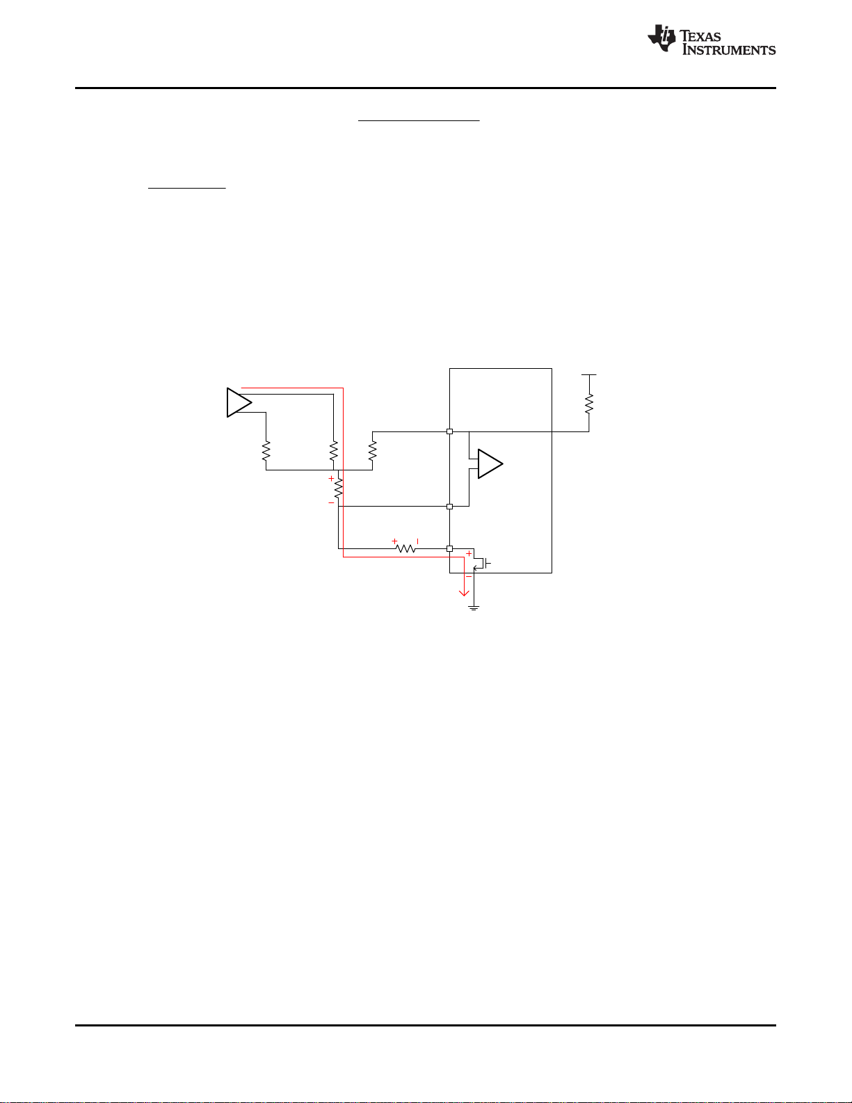
2.2 kΩ
Key R
EQ
R Audio
L Audio
MICBIAS
32 Ω speakers
Jack contact
resistance
20-100 mohm
RING2_SENSE
SLEEVE _SENSE
SLEEVE
Trace routing
resistance
KP ADC
MIC KEY
EQ
MIC KEY
R R
R R
´
=
+
( )
( )
EQ
SLEEVE/ RING2 MICBIAS MICBIAS
2.2k EQ
R
V V V
2.2k R
= + D ´
+ D +
TS3A227E
SCDS358B –NOVEMBER 2014–REVISED FEBRUARY 2015
www.ti.com
(2)
The REQcan be calculated with the following:
(3)
As a result of the above calculations, an ADC attempting to detect the voltage on SLEEVE/RING2 to determine
which key is pressed (whichever is the microphone pin) is reliant on the accuracy on the MICBIAS output and the
2.2 kΩ pull-up resistor. The key press bins are targeted assuming ideal values for these system conditions and
then the gray zone between the bins takes into account the system variations. As a result the better the accuracy
of the MICBIAS output and pull-up resistor the better the accuracy of the key press detection.
In addition to the above, the contact resistance of the audio jack itself can play a role in how accurate the key
press detection is. A general rule is less contact resistance is better. In the figure below a more complete picture
of the system and the voltage the TS3A227E will detect is shown.
The red line denotes the current path for the output of the codec to follow when it enters the speakers and
eventually sinks into the GNDFETs of the TS3A227E. This audio current adds a voltage offset at the audio jack
contact resistance, the trace routing resistance, and the GNDFET itself. Because the TS3A227E has kelvin
connections to the jack via the SLEEVE_SENSE RING2_SENSE pins the trace routing resistance and GNDFET
induced voltage offsets can be compensated.
However, the jack contact resistance is not visible by the device and cannot be compensated for. To maintain the
default bin targets the system must ensure that for a given audio jack contact resistance the max current being
output by the codec/amplifier lies below the curve in Figure 34. This ensures a max error introduced of 5 mV into
the KP detection algorithm.
42 Submit Documentation Feedback Copyright © 2014–2015, Texas Instruments Incorporated
Product Folder Links: TS3A227E

5mV 5mV
2.2
2.2
128
é ù
æ ö
ê ú
ç ÷
æ ö
= ± + + + ´ W + + + ´ W
ê ú
ç ÷
ç ÷
è ø
ê ú
ç ÷
ç ÷
ê ú
è ø
ë û
MICBIAS
Contact MAX
128
R IV´
Contact MAX
MICBIAS
R IV´
TS3A227E
www.ti.com
10.2.2.4.3 Key Press Grey Zones
SCDS358B –NOVEMBER 2014–REVISED FEBRUARY 2015
When defining custom bins and thresholds it is important to also correctly define the “gray zone” between the
bins to ensure that the system will always correctly identify the key that is being pressed. The gray zone region
accounts for the absolute error in key press detection, encompasses the error of the internal ADC along with
errors from system tolerances and variation. The equation below can be used to determine the gray zone
required between each of the bins. Note that the size of the gray zone will vary depending on the actual value of
the key press threshold.
Gray Zone = ± [(Ɛ
TERM DESCRIPTION VALUE UNIT
Ɛ
(ADC,GAIN)
Ɛ
MICBIAS
Ɛ
RBIAS
Internal ADC gain error 0.015%
Codec MICBIAS output voltage variation. Default bin values assume an output variation of 2.5%. 0.025%
MICBIAS resistor variation. Default bin values assume a 1% tolerance of the 2.2 kΩ MICBIAS
resistor.
(ADC,GAIN)
+ Ɛ
MICBIAS
+ Ɛ
RBIAS
+ Ɛ
(CONT,GAIN
) ) × R
(KP Threshold
) + (Ɛ
(ADC,OFF)
+ Ɛ
(CONT,OFF
) + K
0.01%
) × 6 Ω] (4)
BUFF
(1)
(1)
Ɛ
CONT.GAIN
Ɛ
KP Threshold
Ɛ
ADC,OFF
Ɛ
CONT,OFF
K
BUFF
R
Contact
I
MAX
V
MICBIAS
(1) These values can vary depending on the system
Gain error introduced by contact resistance of the audio jack.
KP threshold target identified by system. E.g. the KP Threshold between bins 1 and 2 for the Defined by
default key press bins is 96 Ω. system
Internal ADC offset and linearity error 1.5 LSB
Offset error introduced by contact resistance of the audio jack. LSB
Buffer constant added to total system gray zone to ensure bin values are detected correctly. It is
recommended to use a minimum of 2 for this when defining key gray zones to ensure system 2 LSB
level margins.
Max contact resistance of audio jack Ω
Maximum combined (Right and Left) audio output current into the jack. A
MICBIAS output voltage of the codec V
(1)
Defined by
(1)
system
Defined by
(1)
system
Defined by
(1)
system
Ω
Example Calculation
The default KP Threshold 1 value for the TS3A227E is 10h or 96 Ω. Using the Gray Zone equation the specified
gray zone between keys 1 and 2 can be confirmed assuming the following:
• V
• I
• R
MAX
MICBIAS
(KP Threshold)
× R
= 2.2 V
Contact
= 96 Ω
= 5 mV
• Default values for all other terms
This yields a gray zone of ± 27 Ω. The KP Threshold 1 gray zone can be used to identify the upper limit of key 1
and the lower limit of key 2:
Bin 1 upper limit = KP Threshold 1 – Gray Zone 1
Bin 2 lower limit = KP Threshold 1 + Gray Zone 1
This formula yields an upper limit of 69 Ω. Because each LSB is 6 Ω we round down to the even number of 66 Ω.
For the beginning of key 2 we set the value at (96 Ω + 27 Ω) or 126 Ω (123 Ω rounded up to the nearest LSB).
This method can be used to define the rest of the key bin thresholds.
Copyright © 2014–2015, Texas Instruments Incorporated Submit Documentation Feedback 43
Product Folder Links: TS3A227E
(5)

MICBIAS
enabled
Enable
Key Press Detection
MICBIAS Stable ?4-pole inserted ?Insertion Event
TS3A227E
SCDS358B –NOVEMBER 2014–REVISED FEBRUARY 2015
10.2.2.4.4 Behavior
www.ti.com
The TS3A227E can monitor the microphone line of a 4-pole headset to detect up to 4 key presses/releases and
report the key press events back to the host. The key press detection must be activated manually by setting the
KP Enable bit of the Device Settings 2 register. To ensure proper operation the MICBIAS voltage must be
applied to MICP before enabling key press detection.
Figure 33. Proper Key Press Enable Sequence
The TS3A227E monitors the S3 switch matrix to determine the location of the microphone. If the Manual Switch
Control bit is set to ‘1’, the S3 matrix must be configured in one of the following 2 configurations for the key press
detection to operate. Other configurations are not supported with key press detection.
S3PR S3PS S3GR S3GS MIC LOCATION
On High-Z High-Z On RING2
High-Z On On High-Z SLEEVE
If the voltage on the microphone line drops below the key press detection threshold for a duration longer than the
key press de-bounce time, the key press is considered to be valid. At this point the detected key has the
corresponding Key # Press interrupt bit set to ‘1’ and the interrupt is asserted. The corresponding Key # Release
interrupt is cleared at the same time the Key # Press interrupt is set.
Once the key is released for a duration longer than the key release de-bounce time, a Key Release interrupt is
generated to inform the host that the key has been released. The corresponding Key # released interrupt bit is
set to ‘1’ and the interrupt is asserted.
The Key Press interrupt register will clear the contents and return to the default status of 0h when Key Press
detection is disabled via an I2C write or a removal event.
Notes about key press detection:
• The MICBIAS setting adjusts the detection threshold and must be set to the value that is closest to the
MICBIAS output of the codec. If the MICBIAS voltage being used is between different MICBIAS settings of
the TS3A227E then the closest value that is greater than the MICBIAS voltage should be used.
– E.G. if the codec output is 2.2 V, the 2.3 V MICBIAS setting in the TS3A227E should be used.
• If any pending interrupt is not read by the host and a key is pressed, the TS3A227E will continue to run key
press detection until the Key Press Enable bit is set to ‘0’
The host will interpret Key Press and Release interrupts using the following pseudo-code:
If (Key # Press && Key # Release) {
}
else if (Key # Release ) {
}
else if (Key # Release) {
}
Key # was pressed one time and is not being held.
Key # is being pressed, start the key press duration timer
Key # has been released, end the key press duration timer
The key press duration timer the host starts after reading that a key is pressed can be used as follows:
If (Key # Press Duration Timer > XXX ms) {
The Key # is being held down, handle accordingly.
E.g. if Key # is the volume up key, the system will increment the volume until the Key #
}
Release interrupt is read from the TS3A227E
10.2.2.4.5 Single Key Press Timing
The diagram below depicts a key press event where the MIC is on the SLEEVE pin. If the MIC is on RING2 the
timing diagram will be same.
44 Submit Documentation Feedback Copyright © 2014–2015, Texas Instruments Incorporated
Product Folder Links: TS3A227E
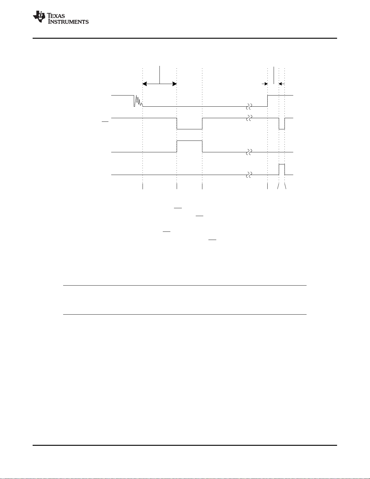
INT
Key Press
De-bounce
(A)
Key Release
De-bounce
(C)
Key 1 Press
Key 1 Release
(D) (E ) (F)(B)
www.ti.com
A. At this point the SLEEVE voltage has stopped glitching and the Key Press De-bounce timer will no longer restart.
B. Point B is the end of the key press de-bounce period. INT will be asserted with the Key Press bit set.
C. The host read and clears the interrupt register, de-asserting the INT pin.
D. Here the key is released and the key release de-bounce period begins.
E. The key release de-bounce period ends and the INT pin is asserted again with the Key Release bit set.
F. Here the host reads and clears the interrupt register, de-asserting the INT pin.
SCDS358B –NOVEMBER 2014–REVISED FEBRUARY 2015
TS3A227E
10.2.2.4.6 Multiple Key Press Timing
The diagram below depicts a multiple key press event in which the host does not immediately read the interrupt
register. The MIC is on the SLEEVE pin in this diagram. If the MIC is on RING2 the timing diagram will be the
same.
NOTE
If the KP Enable bit is set to ‘0’ during key press detection, key press detection will stop
immediately and all the key press/release bits will be cleared.
Copyright © 2014–2015, Texas Instruments Incorporated Submit Documentation Feedback 45
Product Folder Links: TS3A227E
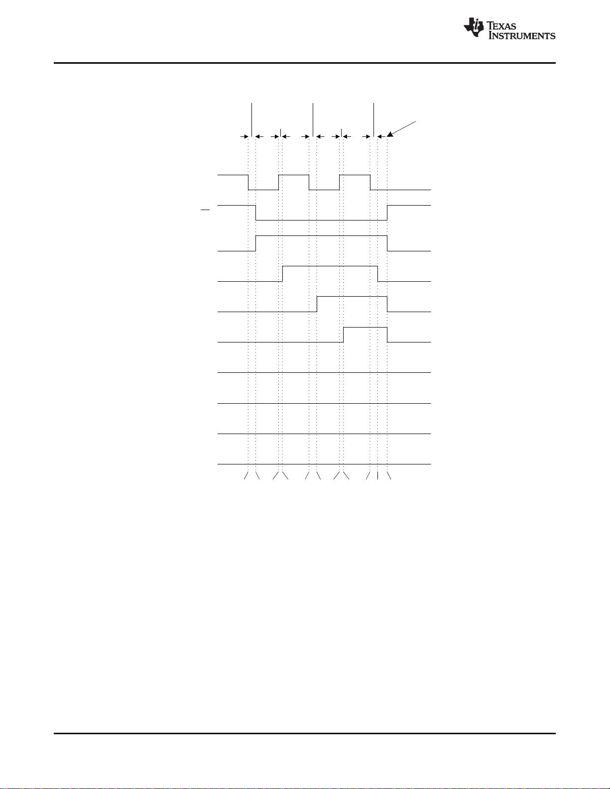
Key 1 Pressed
INT
Key 1 Press
Key 1 Release
Key 2 Press
Key 2 Release
(A) ( B) (C) (D) ( E) (F) (G) (H ) (I) (J ) ( K)
Key 2 Pressed Key 1 Pressed
Key 3 Press
Key 3 Release
Key 4 Press
Key 4 Release
Key Press
De-bounce
Key Press
De-bounce
Key Press
De-bounce
Key Release
De-bounce
Key Release
De-bounce
Host I2C Read
TS3A227E
SCDS358B –NOVEMBER 2014–REVISED FEBRUARY 2015
www.ti.com
A. The SLEEVE voltage drops below the Key Press Detection threshold and the Key Press De-bounce timer is started
B. The end of the key press de-bounce timer. Key 1 is detected, the Key 1 Press interrupt is set and the interrupt line is
asserted. The Key 1 Release interrupt is cleared.
C. The SLEEVE voltage rises to MICBIAS as the key is released. The Key Release de-bounce timer is started.
D. The Key Release de-bounce timer expires. The Key 1 Release bit is set and the interrupt is asserted.
E. The SLEEVE voltage drops below the Key Press Detection threshold and the Key Press De-bounce timer is started
F. The end of the key press de-bounce timer. Key 2 is detected, the Key 2 Press interrupt is set and the interrupt line is
asserted. The Key 2 Release interrupt is cleared.
G. The SLEEVE voltage rises to MICBIAS as the key is released. The Key Release de-bounce timer is started.
H. The Key Release de-bounce timer expires. The Key 2 Release bit is set and the interrupt is asserted.
I. The SLEEVE voltage drops below the Key Press Detection threshold and the Key Press De-bounce timer is started
J. The end of the key press de-bounce timer. Key 1 is detected, the Key 1 Press interrupt is set and the interrupt line is
asserted. The Key 1 Release interrupt is cleared.
K. The host reads the I2C interrupt register and sees the following interrupts:
mmm● Key 1 Press
mmm● Key 2 Press
mmm● Key 2 Release
Using the pseudo-code in the key press detection section this is interpreted as:
mmm● Key 2 was pressed one time and is not being held
mmm● Key 1 is currently pressed, start the key press duration timer
46 Submit Documentation Feedback Copyright © 2014–2015, Texas Instruments Incorporated
Product Folder Links: TS3A227E
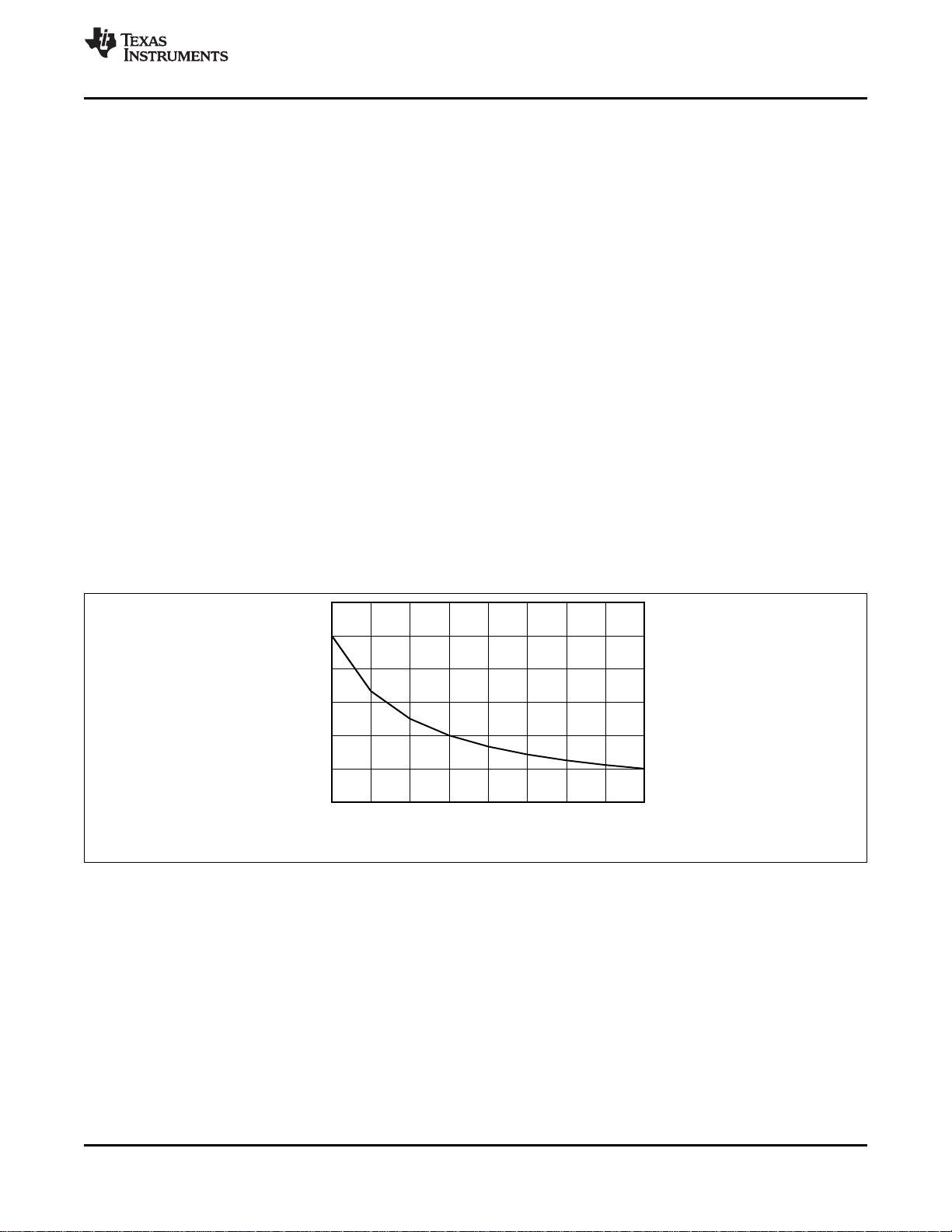
Contact Resistance (m:)
Max Current Supported (mA)
20 30 40 50 60 70 80 90 100
0
50
100
150
200
250
300
D001
TS3A227E
www.ti.com
10.2.2.4.7 Raw Data Key Press Detection
SCDS358B –NOVEMBER 2014–REVISED FEBRUARY 2015
In addition to threshold adjustment the TS3A227E features the ability to utilize the internal ADC raw output with
the Raw Data En bit of the Device Setting 2 register.
Notes on using the Raw ADC Output:
• Key Press/Release interrupts that have not been serviced will not be cleared upon setting the Raw Data En
bit to ‘1’.
• By Setting the Raw Data En bit to ‘1’ the Key Press Threshold registers will be ignored. Instead of reporting
key 1 through 4 press and releases the TS3A227E will only use Key 1 Press to indicate that a key is pressed
and the Key 1 Release interrupt to report that the key was released.
• The ADC Output register will only be cleared after the Raw Data En bit is cleared. The Raw Data En bit is
cleared if the Key Press Enable bit is set to ‘0’. Consequently the ADC Output register clears if the Raw Data
En bit is set to ‘0’, the Key Press Enable bit is set to ‘0’, or a removal event occurs. This means the ADC
Output register will not clear after it is read.
• A manual software trigger can be initiated after a key was pressed to run the ADC detection again. This will
not set the Key 1 Press interrupt.
• The ADC Output is updated after a Key is detected or if the manual ADC trigger bit is set to ‘1’. If an ADC
conversion has completed the ADC Conversion interrupt bit will be set to ‘1’ regardless if there was a
software initiated trigger or if a new key press was detected.
• If the ADC has completed a conversion the output is always non 0 meaning the lowest possible detection
threshold of the ADC is 01h. If the ADC Output register is 00h a conversion has not been completed or the
ADC Output was cleared.
The previous section on gray zones should be applied to any bins create for the raw ADC mode.
10.2.3 Application Curves
Figure 34. Max Current vs Contact Resistance
11 Power Supply Recommendations
The TS3A227E is designed to operate from an input voltage supply range between 2.5 V and 4.5 V. This input
supply is recommended to be decoupled to ground via two de-coupling capacitors of 0.1µF and 1µF placed as
close as possible to the TS3A227E. To ensure a POR trip during a power-down and power-on event the power
supply should follow the minimum and maximum VDDrise and fall times specified in the electrical specifications
section.
The TS3A227E features the ability to power the digital IO pins at a different rail than the supply. This allows
systems to run the TS3A227E at 3.3 V and still use a 1.8 V eliminating the need for a translator. Have the 1.8 V
rail while the device is powered from a higher voltage will increase the current consumption of the device due to
CMOS shoot through current. This increased supply current is documented in the electrical specifications table.
Copyright © 2014–2015, Texas Instruments Incorporated Submit Documentation Feedback 47
Product Folder Links: TS3A227E

MIC_PRESENT
INT
GND
TIP
GND
SDA
VDD
GND_SENS E
MICP
RING2_SENSE
SLEEVE_SEN SE
SLEEVE
SCL
16 15 14 13
5 6 7 8
1
2
3
4
12
11
10
9
DET
TIP
RING1
3.5 mm Jack
RING 2
GNDA
Analog
Ground
VIA to Power Ground Plane
VIA to Bottom Copper or internal layer
Board Edge
to codec
Top Layer Routing
Bottom Layer Routing
RING2
SLEEVE
DET_TRIGGER
TS3A227E
SCDS358B –NOVEMBER 2014–REVISED FEBRUARY 2015
www.ti.com
12 Layout
12.1 Layout Guidelines
• The VDD pin must have de-coupling capacitors places as closely to the device as possible. Typically
recommended capacitors are a 0.1 µF and 1 µF capacitor.
• If FM support is not needed connect GNDA to system GND along with the GND connections with the shortest
connections possible.
• RING2 and SLEEVE should be routed on the same layer as the audio jack for best performance with less
than 50 mΩ to the audio jack pins. These two pins should have priority in layout over other pins. It is
recommended to not use vias on these traces and pair the device with an audio jack that facilitates this type
of layout.
• The RING2_SENSE and SLEEVE_SENSE pins are kelvin connections to the audio jack and should be
shorted to RING2 and SLEEVE as close to the audio jack as possible. If there are 0 Ω resistors between the
SLEEVE/RING2 pins and the jack, connect the SENSE lines to the jack sleeve and ring2 contacts. If a
microphone is connected one of the SENSE lines will carry the microphone signal and the MICBIAS supply. It
is recommended that these traces not have more than 1 Ω impedance to the jack.
• Route the I2C and digital signals away from the audio signals to prevent coupling onto the audio lines.
12.2 Layout Example (QFN)
Figure 35. QFN Layout Example
48 Submit Documentation Feedback Copyright © 2014–2015, Texas Instruments Incorporated
Product Folder Links: TS3A227E

DET
RING1
3.5 mm Jack
Analog Ground
VIA to Power Ground Plane
VIA to Bottom Copper or internal layer
Board Edge
Top Layer Routing
Bottom Layer Routing
4
1
D
C
B
A
2
RING2
/MIC_
PRESENT
/DET_
TRIGGER
SDA
GND
GND
VDD
GNDA
SLEEVE
SLEEVE
TIP
3
RING2
SLEEVE
SENSE
TIP
RING2_
SENSE
SCL
WCSP PAD
MICP
GND_
SENSE
INT
www.ti.com
12.3 Layout Example (DSBGA)
TS3A227E
SCDS358B –NOVEMBER 2014–REVISED FEBRUARY 2015
Figure 36. DSBGA Layout Example
Copyright © 2014–2015, Texas Instruments Incorporated Submit Documentation Feedback 49
Product Folder Links: TS3A227E

TS3A227E
SCDS358B –NOVEMBER 2014–REVISED FEBRUARY 2015
www.ti.com
13 Device and Documentation Support
13.1 Trademarks
All trademarks are the property of their respective owners.
13.2 Electrostatic Discharge Caution
These devices have limited built-in ESD protection. The leads should be shorted together or the device placed in conductive foam
during storage or handling to prevent electrostatic damage to the MOS gates.
13.3 Glossary
SLYZ022 — TI Glossary.
This glossary lists and explains terms, acronyms, and definitions.
14 Mechanical, Packaging, and Orderable Information
The following pages include mechanical, packaging, and orderable information. This information is the most
current data available for the designated devices. This data is subject to change without notice and revision of
this document. For browser-based versions of this data sheet, refer to the left-hand navigation.
50 Submit Documentation Feedback Copyright © 2014–2015, Texas Instruments Incorporated
Product Folder Links: TS3A227E

PACKAGE OPTION ADDENDUM
www.ti.com
10-Dec-2020
PACKAGING INFORMATION
Orderable Device Status
TS3A227ERVAR ACTIVE VQFN RVA 16 3000 RoHS & Green NIPDAU Level-2-260C-1 YEAR -40 to 85 227
TS3A227EYFFR ACTIVE DSBGA YFF 16 3000 RoHS & Green SNAGCU Level-1-260C-UNLIM -40 to 85 227E
(1)
The marketing status values are defined as follows:
ACTIVE: Product device recommended for new designs.
LIFEBUY: TI has announced that the device will be discontinued, and a lifetime-buy period is in effect.
NRND: Not recommended for new designs. Device is in production to support existing customers, but TI does not recommend using this part in a new design.
PREVIEW: Device has been announced but is not in production. Samples may or may not be available.
OBSOLETE: TI has discontinued the production of the device.
Package Type Package
(1)
Drawing
Pins Package
Qty
Eco Plan
(2)
Lead finish/
Ball material
(6)
MSL Peak Temp
(3)
Op Temp (°C) Device Marking
(4/5)
(2)
RoHS: TI defines "RoHS" to mean semiconductor products that are compliant with the current EU RoHS requirements for all 10 RoHS substances, including the requirement that RoHS substance
do not exceed 0.1% by weight in homogeneous materials. Where designed to be soldered at high temperatures, "RoHS" products are suitable for use in specified lead-free processes. TI may
reference these types of products as "Pb-Free".
RoHS Exempt: TI defines "RoHS Exempt" to mean products that contain lead but are compliant with EU RoHS pursuant to a specific EU RoHS exemption.
Green: TI defines "Green" to mean the content of Chlorine (Cl) and Bromine (Br) based flame retardants meet JS709B low halogen requirements of <=1000ppm threshold. Antimony trioxide based
flame retardants must also meet the <=1000ppm threshold requirement.
(3)
MSL, Peak Temp. - The Moisture Sensitivity Level rating according to the JEDEC industry standard classifications, and peak solder temperature.
(4)
There may be additional marking, which relates to the logo, the lot trace code information, or the environmental category on the device.
(5)
Multiple Device Markings will be inside parentheses. Only one Device Marking contained in parentheses and separated by a "~" will appear on a device. If a line is indented then it is a continuation
of the previous line and the two combined represent the entire Device Marking for that device.
(6)
Lead finish/Ball material - Orderable Devices may have multiple material finish options. Finish options are separated by a vertical ruled line. Lead finish/Ball material values may wrap to two
lines if the finish value exceeds the maximum column width.
Important Information and Disclaimer:The information provided on this page represents TI's knowledge and belief as of the date that it is provided. TI bases its knowledge and belief on information
provided by third parties, and makes no representation or warranty as to the accuracy of such information. Efforts are underway to better integrate information from third parties. TI has taken and
continues to take reasonable steps to provide representative and accurate information but may not have conducted destructive testing or chemical analysis on incoming materials and chemicals.
TI and TI suppliers consider certain information to be proprietary, and thus CAS numbers and other limited information may not be available for release.
In no event shall TI's liability arising out of such information exceed the total purchase price of the TI part(s) at issue in this document sold by TI to Customer on an annual basis.
Samples
Addendum-Page 1

PACKAGE OPTION ADDENDUM
www.ti.com
10-Dec-2020
Addendum-Page 2

PACKAGE MATERIALS INFORMATION
www.ti.com 14-Sep-2018
TAPE AND REEL INFORMATION
*All dimensions are nominal
Device Package
TS3A227ERVAR VQFN RVA 16 3000 330.0 12.4 3.75 3.75 1.15 8.0 12.0 Q2
TS3A227EYFFR DSBGA YFF 16 3000 180.0 8.4 1.94 1.94 0.69 4.0 8.0 Q1
Type
Package
Drawing
Pins SPQ Reel
Diameter
(mm)
Reel
Width
W1 (mm)
A0
(mm)B0(mm)K0(mm)P1(mm)W(mm)
Pin1
Quadrant
Pack Materials-Page 1
PACKAGE MATERIALS INFORMATION
www.ti.com 14-Sep-2018
*All dimensions are nominal
Device Package Type Package Drawing Pins SPQ Length (mm) Width (mm) Height (mm)
TS3A227ERVAR VQFN RVA 16 3000 367.0 367.0 35.0
TS3A227EYFFR DSBGA YFF 16 3000 182.0 182.0 20.0
Pack Materials-Page 2

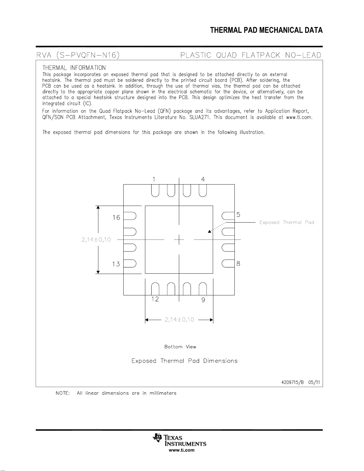

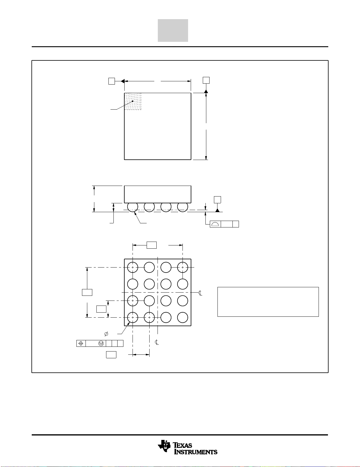
PACKAGE OUTLINE
BALL A1
CORNER
0.625 MAX
0.30
0.12
B E
BALL TYP
SCALE 8.000
DSBGA - 0.625 mm max heightYFF0016
DIE SIZE BALL GRID ARRAY
A
D
C
SEATING PLANE
0.05 C
1.2 TYP
D
C
1.2
TYP
0.4 TYP
16X
0.015 C A B
NOTES:
1. All linear dimensions are in millimeters. Any dimensions in parenthesis are for reference only. Dimensioning and tolerancing
per ASME Y14.5M.
2. This drawing is subject to change without notice.
B
A
0.3
0.2
0.4 TYP
1
2
3
SYMM
SYMM
D: Max =
E: Max =
4
1.786 mm, Min =
1.786 mm, Min =
4219386/A 05/2016
1.726 mm
1.726 mm
www.ti.com

16X ( 0.23)
(0.4) TYP
EXAMPLE BOARD LAYOUT
DSBGA - 0.625 mm max heightYFF0016
DIE SIZE BALL GRID ARRAY
(0.4) TYP
1
A
3
2
4
( 0.23)
METAL
SOLDER MASK
OPENING
B
C
D
LAND PATTERN EXAMPLE
NON-SOLDER MASK
DEFINED
(PREFERRED)
SYMM
SCALE:30X
0.05 MAX
0.05 MIN
SYMM
METAL UNDER
SOLDER MASK
( 0.23)
SOLDER MASK
OPENING
SOLDER MASK
DEFINED
SOLDER MASK DETAILS
NOT TO SCALE
4219386/A 05/2016
NOTES: (continued)
3. Final dimensions may vary due to manufacturing tolerance considerations and also routing constraints. For more information,
see Texas Instruments literature number SNVA009 (www.ti.com/lit/snva009).
www.ti.com
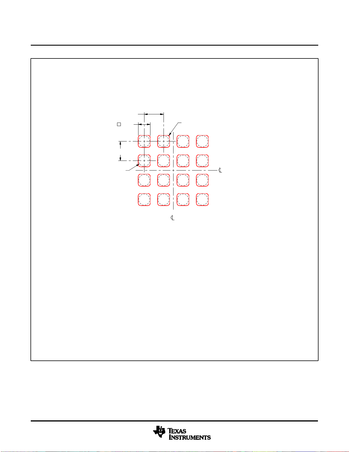
(0.4) TYP
16X ( 0.25)
EXAMPLE STENCIL DESIGN
DSBGA - 0.625 mm max heightYFF0016
DIE SIZE BALL GRID ARRAY
(R0.05) TYP
1
2
A
3
4
(0.4) TYP
METAL
TYP
B
SYMM
C
D
SYMM
SOLDER PASTE EXAMPLE
BASED ON 0.1 mm THICK STENCIL
SCALE:30X
NOTES: (continued)
4. Laser cutting apertures with trapezoidal walls and rounded corners may offer better paste release.
www.ti.com
4219386/A 05/2016

IMPORTANT NOTICE AND DISCLAIMER
TI PROVIDES TECHNICAL AND RELIABILITY DATA (INCLUDING DATASHEETS), DESIGN RESOURCES (INCLUDING REFERENCE
DESIGNS), APPLICATION OR OTHER DESIGN ADVICE, WEB TOOLS, SAFETY INFORMATION, AND OTHER RESOURCES “AS IS”
AND WITH ALL FAULTS, AND DISCLAIMS ALL WARRANTIES, EXPRESS AND IMPLIED, INCLUDING WITHOUT LIMITATION ANY
IMPLIED WARRANTIES OF MERCHANTABILITY, FITNESS FOR A PARTICULAR PURPOSE OR NON-INFRINGEMENT OF THIRD
PARTY INTELLECTUAL PROPERTY RIGHTS.
These resources are intended for skilled developers designing with TI products. You are solely responsible for (1) selecting the appropriate
TI products for your application, (2) designing, validating and testing your application, and (3) ensuring your application meets applicable
standards, and any other safety, security, or other requirements. These resources are subject to change without notice. TI grants you
permission to use these resources only for development of an application that uses the TI products described in the resource. Other
reproduction and display of these resources is prohibited. No license is granted to any other TI intellectual property right or to any third
party intellectual property right. TI disclaims responsibility for, and you will fully indemnify TI and its representatives against, any claims,
damages, costs, losses, and liabilities arising out of your use of these resources.
TI’s products are provided subject to TI’s Terms of Sale (www.ti.com/legal/termsofsale.html) or other applicable terms available either on
ti.com or provided in conjunction with such TI products. TI’s provision of these resources does not expand or otherwise alter TI’s applicable
warranties or warranty disclaimers for TI products.
Mailing Address: Texas Instruments, Post Office Box 655303, Dallas, Texas 75265
Copyright © 2020, Texas Instruments Incorporated
 Loading...