

Page 1

Evaluation Board Documentation
TRF1500 Integrated Dual-Band
RF Receiver User’s Guide
APPLICATION BRIEF: SWRA004A
Wireless Communications Business Unit
Digital Signal Processing Solutions
July 98
Page 2

IMPORTANT NOTICE
Texas Instruments (TI) reserves the right to make changes to its products or to discontinue any
semiconductor product or service without notice, and advises its customers to obtain the latest version of
relevant information to verify, before placing orders, that the information being relied on is current.
TI warrants performance of its semiconductor products and related software to the specifications applicable
at the time of sale in accordance with TI’s standard warranty. Testing and other quality control techniques
are utilized to the extent TI deems necessary to support this warranty. Specific testing of all parameters of
each device is not necessarily performed, except those mandated by government requirements.
Certain application using semiconductor products may involve potential risks of death, personal injury, or
severe property or environmental damage (“Critical Applications”).
TI SEMICONDUCTOR PRODUCTS ARE NOT DESIGNED, INTENDED, AUTHORIZED, OR WARRANTED
TO BE SUITABLE FOR USE IN LIFE-SUPPORT APPLICATIONS, DEVICES OR SYSTEMS OR OTHER
CRITICAL APPLICATIONS.
Inclusion of TI products in such applications is understood to be fully at the risk of the customer. Use of TI
products in such applications requires the written approval of an appropriate TI officer. Questions concerning
potential risk applications should be directed to TI through a local SC sales office.
In order to minimize risks associated with the customer’s applications, adequate design and operating
safeguards should be provided by the customer to minimize inherent or procedural hazards.
TI assumes no liability for applications assistance, customer product design, software performance, or
infringement of patents or services described herein. Nor does TI warrant or represent that any license,
either express or implied, is granted under any patent right, copyright, mask work right, or other intellectual
property right of TI covering or relating to any combination, machine, or process in which such
semiconductor products or services might be or are used.
Copyright © 1998, Texas Instruments Incorporated
Page 3

TRADEMARKS
TI i s a trad emark of Texas Instrum ents Inc orporated .
Other brands and names are the property of their respective owners.
Page 4

CONTACT INFORMATI ON
PIC TELEPHONE (972) 644-5580
PIC FAX (972) 480-7800
HP SUPPORT LI N E (972) 480- 7 87 2
PIC email sc-infomaster@ti.com
Page 5

Contents
Abstract.........................................................................................................................9
Product Support .........................................................................................................10
The TI Advantage Extends Beyond RF to Every Other Major Wireless System
Block.......................................................................................................................10
Related Documentation...........................................................................................11
World Wide Web.....................................................................................................11
Email.......................................................................................................................11
Introducti on.................................................................................................................12
Design Considerations...............................................................................................13
External Components..............................................................................................13
Board Design and Impedance Matching..................................................................13
TRF 1500 Dual-Band Receiver ...................................................................................14
TRF1500 Control State ...............................................................................................17
Low Band Cascaded Receiver Section: LNA, External SAW Filter, Mixer, and LO
Buffer Amplifier...........................................................................................................18
Low-Band LNA........................................................................................................19
Low-Band LNA Turn on Time..................................................................................19
Low-Band LNA Input...............................................................................................20
Low-Band LNA Output............................................................................................20
Surface Acoustic Wave (SAW) Filter.......................................................................21
Low-Band Mixer......................................................................................................22
Low-Band Mixer RF Input .......................................................................................22
Low-Band Mixer LO Input .......................................................................................23
Low-Band IF Output................................................................................................23
Low-Band LO Buffer Amplifier Output.....................................................................24
Low-Band Cascaded Test Guide ...............................................................................26
LOW-Band Cascaded: Power Conversion Gain......................................................26
Low-Band Cascaded: Power Conversion Gain Reduction.......................................27
Low-Band Cascaded: Noise Figure.........................................................................28
Low-Band Cascaded: RF Input Return Loss...........................................................30
Low-Band Cascaded: LO Input Return Loss...........................................................30
LOW BAND: LO Buffer Out pu t Power.....................................................................31
Low-Band: Power Leakage LO In to RF In..............................................................31
Low-Band Cascaded: Third Order Input Intercept Point (IIP3).................................32
Low-Band Cascaded: 1dB RF Input Compression Point.........................................33
Low-Band Cascaded: 1dB Blocking Point...............................................................34
High-Band Cascaded Receiver Section: LNA, Mixer, LO Buffer Amplifier .............35
Cascaded High-Band Receiver Section: LNA, Mixer, and LO Amplifier...................35
High-Band RF Input................................................................................................36
High-Band LO Input................................................................................................36
High-Band IF Output...............................................................................................38
High-Band LO Buffer Amplifier Output ....................................................................39
High-Band Cascaded Test Guide...............................................................................40
High-Band Cascaded: Power Conversion Gain.......................................................40
Page 6

Contents
High-Band Cascaded: Power Conversion Gain Reduction......................................41
High-Band Cascaded: Image Rejection...................................................................42
High-Band Cascaded: Noise Figure........................................................................43
High-Band Cascaded: RF Input Return Loss ..........................................................44
High-Band : LO Bu ffer Out pu t Power.......................................................................45
High-Band Cascaded: Power Leakage LO In to RF In ............................................46
High-Band Cascaded: Third Order Input Intercept Point (IIP3)................................46
High-Band Cascaded: 1dB Input Compression Point..............................................47
High-Band Cascaded: 2X2 Spur Performance........................................................48
High Band: 3X3 Spur Performance.........................................................................49
Low-Band and High-Band Transmit ..........................................................................50
Low- and High-Band Transmit Mixer.......................................................................50
Low-Band and High-Band Transmit Mixer RF Input ................................................50
Low- and High-Band Transmit Mixer IF Output .......................................................51
Low-Band Transmit Mixer Test Guide.......................................................................52
Low-Band Transmit Mixer: Power Conversion Gain................................................52
Low-Band Transmit Mixer: Noise Figure .................................................................53
Low-Band Transmit Mixer: Input Return Loss..........................................................54
Low-Band Transmit Mixer: Power Leakage LO In to TX In......................................55
Low-Band Transmit Mixer: Power Leakage TX In to LO In......................................55
Low-Band Transmit Mixer: 1dB Input Compression Point .......................................56
Low-Band Transmit Mixer: Second Order Input Intercept Point (IIP2).....................57
Low-Band Transmit Mixer: Third Order Input Intercept Point (IIP3).........................58
High-Band Transmit Mixer Test Guide......................................................................59
Low-Band LNA Stand-Alone Test Guide...................................................................60
Low-Band LNA: Gain ..............................................................................................60
Low-Band LNA: Input Return Loss..........................................................................60
Low-Band LNA: Output Return Loss.......................................................................61
Low-Band LNA: Isolation.........................................................................................61
Low-Band LNA: 1dB Input Compression Point ........................................................61
Low-Band LNA: Noise Figure..................................................................................62
Low-Band LNA: Third Order Input Intercept Point (IIP3)..........................................63
Low-Band Receiver Mixer Stand-Alone Test Guide .................................................65
Low-Band Receiver Mixer: Power Conversion Gain................................................65
Low-Band Receiver Mixer: Input Return Loss.........................................................66
Low-Band Receiver Mixer: Power Leakage LO In to RF In......................................67
Low-Band Receiver Mixer: Noise Figure.................................................................67
Low-Band Receiver Mixer: 1dB RF Input Compression Point..................................69
Low-Band Receiver Mixer: Third Order Input Intercept Point (IIP3).........................70
Appendix A: Test Bench Configuration.....................................................................72
Page 7

Figures
Figure 1. TRF1500 Dual-Band Receiver Block Diagram................................................14
Figure 2. Cascaded Block Diagram of the Low-Band Receiver Section.........................18
Figure 3. Voltage Divider at Low-Band LNA Input..........................................................19
Figure 4. Low- Ba nd LN A In pu t Co n figur ation...................................................................20
Figure 5. Low- Ba nd LN A Ou tp ut C onfi gur a ti o n.................................................................21
Figure 6. SA W Filter Inserti o n Loss..................................................................................21
Figure 7. Low-Band Mixer RF Input Configuration ............................................................22
Figure 8. Low-Band Mixer LO Input Configuration............................................................23
Figure 9. Low-Band IF Output Configuration....................................................................24
Figure 10. Low-Band Buffer Amplifier Output Configuration .............................................25
Figure 11. Block Diagram of the High-Band Receiver Section..........................................35
Figure 12. High-Band RF Input Configuration...................................................................36
Figure 13. High-Band LO Frequency Doubler Driven Configuration .................................37
Figure 14. High-Band LO Directly Driven Configuration....................................................37
Figure 15. High-Band IF Output Configuration..................................................................38
Figure 16. High-Band LO Buffer Amplifier Output Configuration.......................................39
Figure 17. Transmit Mixer Block Diagram.........................................................................50
Figure 18. Low- and High-Band Transmit Mixer RF Input Configuration...........................51
Figure 19. Low- and High-Band Transmit Mixer IF Output Configuration..........................51
Figure 20. Test Bench Setup: Power Conversion Gain, Power Conversion Gain
Reduction, 1dB RF Input Compression Point, Second Order Input Intercept
Point (IIP2), 2x2 Spur Perform ance, 3x3 Spur Performance, Ima ge rej ec tion
and LO Buffer Output Power...........................................................................72
Figure 21. Test Bench Setup: Third Order Input Intercept Point (IIP3), 1dB Blocking
Point Measurements.......................................................................................72
Figure 22. Test Bench Setup: Noise Figure .....................................................................73
Figure 23. Test Bench Setup: Power Leakage LO In to RF In .........................................73
Figure 24. Test Bench Setup: Power Leakage RF In to LO In Measurements.................74
Figure 25. Test Bench Setup: LNA Noise Figure Measurements .....................................74
Figure 26. Test Bench Setup: LNA Third Order Input Intercept Point (IIP3) Measurement75
Figure 27. Test Bench Setup: LNA 1dB Input Compression Point...................................75
Tables
Table 1. Pin Descriptions.................................................................................................15
Table 2. Control State and the Corresponding Active Circuits.........................................17
Table 3. LB LNA, LB Mixer, SAW Filter, and LB IF Amp Parameters...............................26
Table 4. HB LNA, HB mixer, HB IF amp..........................................................................40
Table 5. Low-Band Transmit Performance Parameters...................................................52
Table 6. High-Band Transmit Mixer Performance Parameters.........................................59
Table 7. Low-Band LNA Parameters...............................................................................60
Table 8. Low-Band Receiver Mixer Parameters..............................................................65
Page 8

TRF1500 Integrated Dual-Band RF
Abstract
Receiver User’s Guide
The dual-band handset market is expanding very rapidly due to
the increase in customers requiring roaming capa bility. The
customer also demands that handsets have an increase in
features while keeping the size compact. These dual-band
handset requirements put pressure on the integrated circuit
manufacturer to be innovative while keeping costs low.
To meet this demand, Texas Instruments (TI) has developed the
TRF1500 receiver. The TRF1500 is a fully-integrated dual-band
receiver in a single package. The selection of the external
components and the layout of the system board required to
complete a tr ans ceiver des ign are cri ti c al t o achi eve maxim um
perform ance.
This application report discusses the implementation and
impedance matching of each section of the TRF1500 to keep the
required board area to a minimum and minimizing external
components while maximizing performance. It also discusses
parameter measurement techniques.
TRF1500 Integrat ed Dual- B and RF Receiver User’s Guide 9
Page 9
SWRA004A
Product Suppor t
The TI Advan ta ge E xt en ds Be yon d RF to E very Other Major
Wireless System Block
Speaker
Speaker
Audio
Audio
Interface
Interface
Microphone
Microphone
SINGLE CHIP ANAL OG
BASEBAND
TMS320C54X
TMS320C54X
DSP Core
DSP Core
S/W
S/W
ASIC
TSC6000
SINGLE CHIP DIGIT AL BASE BAND
ARM7TDMIE
BACKPLANE
Microcontroller
Microcontroller
ARM7TDMIE
(C470)
(C470)
S/W
S/W
RF
RF
Interface
Interface
User Display
User Display
Keyboard
Keyboard
SIM Card
SIM Card
Receiver
Receiver
TRF1xxx
TRF1xxx
Synthesizer
Synthesizer
TRF2xxx
TRF2xxx
Modulator
Modulator
TRF3xxx
TRF3xxx
RF SE CTION
Op Amps
Op Amps
Switches
Switches
Regulators
Regulators
POW E R MGMT
Power A mp
Power A mp
TRF7xxx,
TRF7xxx,
TRF8xxx
TRF8xxx
Digital Baseband
TI’s single-chip Digital Baseband Platform, combines two high-performance core
processors – a digital signal processor tailored for digital wireless applications and a
microcontroller designed specifically for low-power embedded systems. The
customizable platform helps wireless digital telephone manufacturers lower component
counts, save board space, reduce power consumption, introduce new features, save
development costs and achieve faster time to market, at the same time giving them
flexibility and performance to support any standard worldwide.
Analog Baseband
TI analog baseband components provide a Mixed-signal bridge between the real world
of analog si g nal s an d di gi t al sig nal pr ocessors, the key en abli n g t ec hnology of the digital
wireless industry. Using a seamless architecture for wireless communications
technology, TI matches its baseband interfaces, radio frequency ICs and power
managem en t I Cs to digital signal pr ocessing engines t o cre at e complete DSP Solutio ns
for digital wireless systems.
Power Management
TI provides power management solutions with integration levels designed to meet the
needs of a ran ge o f wireless applicatio ns . From di s cr et e LD Os an d v olt a ge supervisors
to complete power supplies for the baseband section, TI power ma nagement solutions
play an important role in increasing wireless battery life, time-to-market and system
functionality.
For more information visit the Wireless Communications web site at
www.ti.com/sc/docs/wireless/home.htm.
10 TRF1500 Integrat ed Dual- B and RF Receiver User’s Guide
Page 10

SWRA004A
Related Documentation
The following list specifies product names, part numbers, and
literature numbers of corresponding TI documentation.
Dual-Band/Dual-Mode PCS Receiver
❑
SLWS041A
World Wide Web
Our World Wide Web site at www.ti.com contains the most up to
date product information, revisions, and additions. Users
registering with TI&ME can build custom information pages and
receive new product updates automatically via email.
Email
For technical issues or clarification on switching products, please
send a detailed email to sc-infomaster@ti.com. Questions receive
prompt attention and are usually answered within one business
day.
, Literature number
TRF1500 Integrat ed Dual- B and RF Receiver User’s Guide 11
Page 11

Introduc ti on
SWRA004A
The TRF1500 is a dual-band/dual-mode Personal
Communications Syste m (PCS) receiver for cellular telephones
operating dual mode (a nalog and digital) in the 800 MHz band and
single mode (digital) in the 1900 MHz band. The TRF1500
consists of a low noise amplifier (LNA) and mixer for each band.
For image rejection, the low-ba nd receiver relies on an off-chip
image rejection filter between the LNA and mixer while the highband receiver uses an image rejection mixer. The device operates
from a single 3.75 volt supply and is controlled by six digital
CMOS control lines. The digital control offers a wide range of
control states, including a sleep mode where the device typically
draws less than 5µA.
Additionally, the local o scillator (LO) inputs have buffered outputs
that can be used in either single-ended or differential mode for a
phase-locked-loop (PLL) configuration. A state is also available
that allows the low-band LO to serve as the high-band LO through
a mode-selectable frequency doubler.
A wide-ba nd mix er is als o avai l a bl e for tr ansm i t loo p ar chi t ec t ur es
which are commonly used in advanced mobile phone systems,
global systems for mobile communications and other digital
systems.
The TRF1500 is available in a 48-pin plastic thin quad flatpack
package and is characterized for operation from -40C to 85C
operatin g fr ee- ai r tem p er ature.
Please refer to the data sheet for the TRF1500 (TI literature
number SLWS041A) for detailed information on the device
specifications and refer to the users guide for test instructions (TI
literature number SWRA004A).
12 TRF1500 Integrat ed Dual- B and RF Receiver User’s Guide
Page 12

SWRA004A
Design Conside ra ti ons
The successful integration of a TRF1500 receiver device into a
design is dependent upon the performance of the external
components and the quality of the board design and layout.
Ex ternal Componen ts
Componen t tolerance and Q specifications (where applicable)
should be obs er ve d dur i n g the selecti o n o f any exte rnal
components. The TRF1500 data sheet, TI literature number
SLWS041A, includes a Bill of Mate rials (BOM) detailing
components with proven performance, that are used on the
evaluation board. The location and orientation of components
should also be taken into consideration for maximum performance
and manufacturability. For e xamp le, the lo w-ba nd imag e rejection
is dependent on an external Surface Acoustic Wave (SAW)
component. This filter is used to reject signal outside the band of
the receiver and has bee n chosen to maximize the TR F1500
performance, while maintaining minimum size and cost.
Board Design and Impedance Matching
The quality of the board layout is also critical to the TRF1500
performance. Co rrect transmission line impedances must be
maintained throughout the design to insure maximum
performance. Co rrect transmission line impedances can be
maintained by using proper line widths and board stack-up in
relation to the dielectric constant of the board material.
Utilizing the correct external component to match the device
impedance to board transmission line impedance is also very
important.
For measurement simplicity, the e valuation board utilizes RF
Balun transformers for impedance matching selected differential
inputs and outputs to single-ended inpu ts and outputs. Please
note that the Baluns are used only for evaluating the device on the
evaluation board and do not have to be included in the end user’s
application.
To minimize unwanted signal interference and coupling, digital
lines should be routed around and away from the receiver. On a
multi-layer board, running a separate plane for the digital lines is
highly recommended. Power supply lines should be filtered and
regulate d as clo se as poss ible at the device term i nal.
TRF1500 Integrat ed Dual- B and RF Receiver User’s Guide 13
Page 13
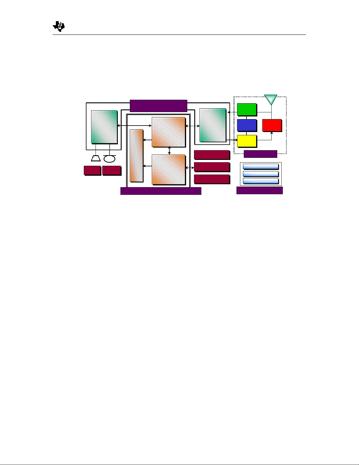
TRF 1500 Dual-Band Receiver
A block diagram of the TRF1500 dual-band receiver front end
down converter is shown in Figure 1. Pin names and descriptions
are provided in Table 1. The device operates from a single 3.75
volt supply and its operation is controlled by 6 digital CMOS
control lines the TRF1500 operates in 18 different states. The
control codes and the corresponding active circuits are given in
Table 2.
Figure 1. TRF1500 Dual-Band Receiver Block Diagram
SWRA004A
14 TRF1500 Integrat ed Dual- B and RF Receiver User’s Guide
Page 14

SWRA004A
Table 1. Pin Descriptions
Pin Number Name Description
1 Bias Adjust Bias adjust
2 TX IF + Transmit IF, noninverting output
3 TX IF - Transmit IF, inv er ting output
4 GND ground
5 MIX IN LOW BAND Low band mixer input
6 GND ground
7VCC Vcc
8 GND Ground
9 TX + Transmit, noninverting input
10 TX - Transmit, inverting input
11 GND Ground
12 IR ADJUST D Image rejection adjustment
13 HI/LO High band/low band select
14 SYN ON VCO power control
15 HIGH BAND IF + High band IF noninvert ing output
16 HIGH BAND IF - High band IF, inver ting output
17 LOW BAND IF + Low band IF noninverting output
18 LOW BAND IF - Low band IF, inverting output
19 GND ground
20 HIGH BAND LO + High band noninverting LO output
21 HIGH BAND LO - High band, inv erti ng LO out put
22 LOW BAND LO + Low band noninverting LO output
23 LOW BAND LO - Low band, inv er ting LO output
24 RX ON Low noise amplifier/mixer power control
25 VCC Vcc
26 TX ON Transmit mixer/driver power control
27 HIGH BAND LO IN -/RF GND High band LO inverting input/RF GND
28 HIGH BAND LO IN + High band LO noninverting input
29 GND ground
30 DOUDLER TANK Doubler output
31 VCC VCC
32 LOW BAND LO IN Low band LO input
33 GND ground
34 GND ground
35 X2 ON Doubler power control
36 IR ADJUST A Image rejection adjustm ent
37 IR ADJUST B Image rejection adjustm ent
TRF1500 Integrat ed Dual- B and RF Receiver User’s Guide 15
Page 15

38 STRONG SIGNAL Strong signal indication
39 GND ground
40 VCC VCC
41 GND ground
42 LNA IN HIGH BAND High band LNA input
43 LNA IN LOW BAND Low band LNA input
44 GND ground
45 LNA OUT LOW BAND Low band LNA output
46 GND ground
47 GND ground
48 IR ADJUST C Image rejection adjustment
SWRA004A
16 TRF1500 Integrat ed Dual- B and RF Receiver User’s Guide
Page 16

SWRA004A
TRF1500 Control State
The TRF1500 operates in 18 different states: The control code
and active circuits are given in Table 2.
Table 2. Control State and the Corresponding Active Circuits
Control Code
(HI/LO, SYN ON, RX ON, TX ON, STRONG SIGNAL, X2)
000000 Sleep Mode
010000 Low-Band LO Input Buffer On LB LO Buffer
011000 Low-Band Receive Normal LB LO Buffer, LB LNA, LB Mixer
011010 Low-Band Receive Strong Signal LB LO Buffer, LB Mixer
010100 Low-Band Transmit Mixer LB LO Buffer, LB TX Mixer
011100 Low-Band Receive and Transmit Mixer LB LO Buffer, LB LNA (On High), LB Mixer , LB TX
011110 Low-Band Transmit Mixer LB LO Buffer, LB LNA (On High), LB Mixer
010001 Doubler On LB LO Buffer, Frequency Doubler, HB LO Buffer
011001 Low-Band Receive Normal, Doubler On
011011 Low-Band Receive Strong Signal, DoublerOnLB LO Buffer, LB Mixer, Fr equenc y Doubler
011111 Low-Band Transmit, Doubler On LB LO Buffer, LB LNA (On High), LB Mixer, LB TX
111011 High-Band Receive Strong Signal, DoublerOnHB LO Buffer, HB Mixer, Fr equenc y Doubler
110000 High-Band LO Input B uff er On HB LO Buffer
111000 High-Band Receive Normal HB LO Buffer, HB LNA, HB Mixer
111010 High-Band Receive Strong Signal HB LO Buffer, HB Mixer
111001 High-Band Receive Frequency, Doubler On LB LO Buff er, HB LO Buffer, HB LNA, HB Mixer,
110100 High-Band Transmit Normal HB LO Buffer, HB TX Mixer
110101 High-Band Transmit Frequency, Doubler
On
Active Circuits
Mixer
LB LO Buffer, LB LNA, LB Mixer, F r equenc y
Doubler
Mixer
Frequency Doubler
HB LO Buffer, HB TX Mixer, Frequency Doubler,
LB LO Buffer
TRF1500 Integrat ed Dual- B and RF Receiver User’s Guide 17
Page 17
SWRA004A
Low Band Cascaded Receiver Section: LNA, External SAW
Filter, Mixer, and LO Buffer Ampli f ier
The TRF1500 low-band receiver section, shown in Figure 2, is an
integrated front-end down converter designed to operate in the
800 MHz frequency range. The low-band down converter consists
of an LNA, mixer, LO buffer amplifier and an off-chip image reject
filter. The digital control allows the low-band to operate in thre e
different states to compensate for the environment in which the
TRF1500 is operating. The device can be operated in the normal
state, where the LNA, mixer and buffer amplifier are on, the strong
signal state, where the LNA is off and the mixer and buffer
amplifier are on, or the transmit state, where the LNA bias current
is increased to prevent compression when the transmitter is on.
The low-band receiver has low typical current consumption of
21mA at 3.75V supply. The cascaded gain is typically 26dB while
providing good dynamic range with approximately a -10dBm third
order input intercept point (IIP3). The low-band receiver has a
typical system noise figure of approximately 2.5 dB for excellent
sensitivity.
Figure 2. Cascaded Block Diagram of the Low-Band Receiver Section
18 TRF1500 Integrat ed Dual- B and RF Receiver User’s Guide
Page 18
SWRA004A
Low-B an d LNA
In a typical down-conversion receiver, the LNA is usually placed
directly after the antenna and a band-select filter. The purpose of
the LNA is to amplify the desired signal being received while
adding as little undesired noise and distortion as possible. The
TRF1500 LNA is a common emitter amplifier, designed to operate
on a single 3.75 volt supply. The LNA has two selectable gain
states, normal state or strong signal state, which are controlled
with the digital CMOS control lines. The strong signal state, which
disables the LNA, is provided for operation in a high signal
environment such as near the base station. Operating near the
base station in the normal state could cause an increase in the
intermodulation product levels and thus cause undesired noise
and distortion in the receiver. Stand-alone LNA performance can
be ascertained by reconfiguring the evaluation board as noted on
the da tashee t.
Low-B an d LNA Turn on Tim e
The turn on time can be adjusted by changing the values of C10,
R6 and R7, as shown in Figure 3 and Figure 4. The resistors form
a voltage-divider network across the supply, Vcc. The function of
this network is to provide a bias condition near the ideal operating
region at the base of the common emitter amplifier. By providing
this bias condition, the charge time of the series capacitor, C10,
can be ad justed. Changing the value of resistors should not affect
gain, IIP3 or noise figure (NF) performance.
Figure 3. Voltage Divider at Low-Band LNA Input
TRF1500 Integrat ed Dual- B and RF Receiver User’s Guide 19
Page 19
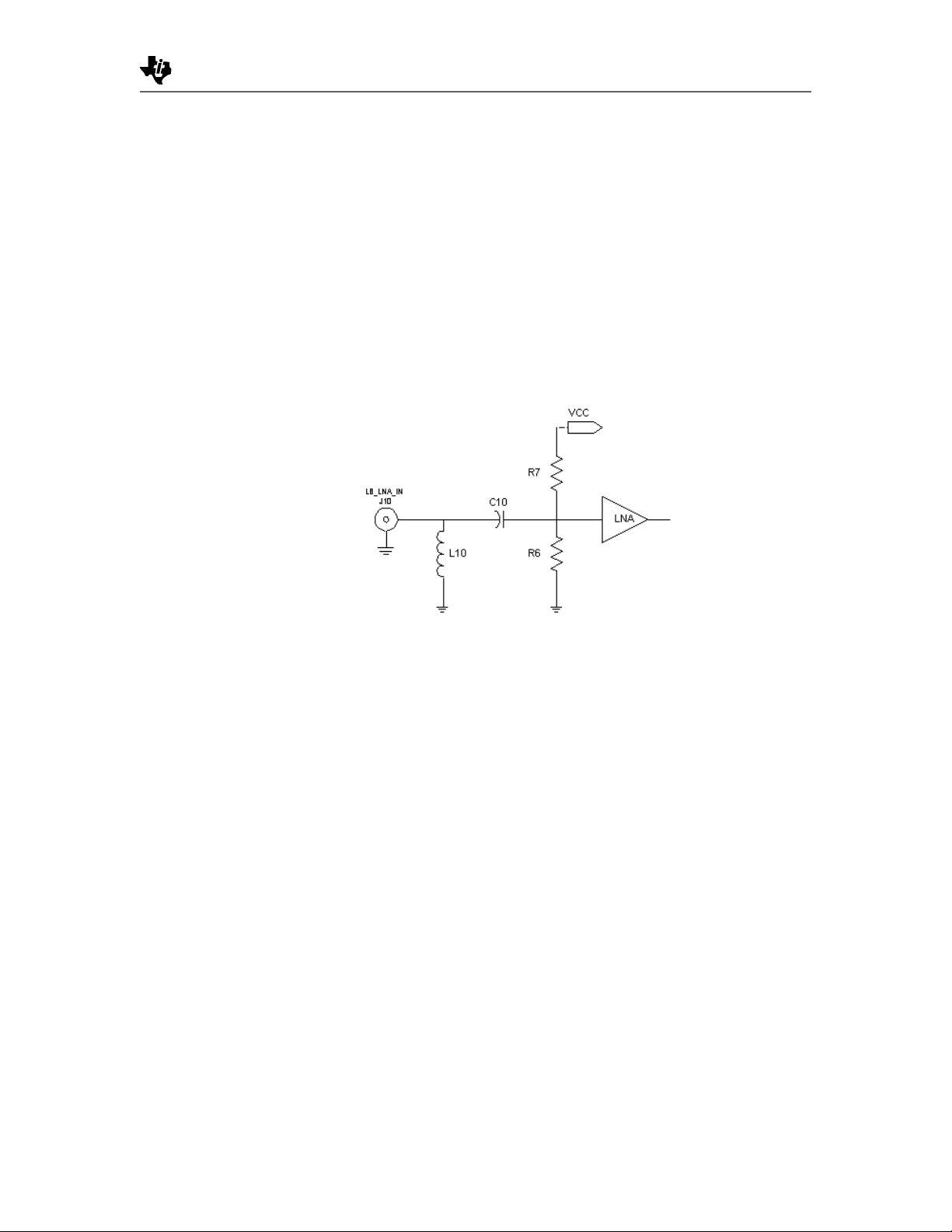
Low-B an d LNA Input
Figure 4 details the lo w-band LNA input configuration. The LNA
input impedance matching network primarily determines the
cascaded gain, noise figure, and input return loss performance of
the low-band receiver section. A simple high-pass shunt-L (L10)
impedance matching network is used for optimum noise figure
performance. The trade off for this optimization is a lower input
return loss in the pass-band, but with sufficient attenuation in the
stop-band. C10 has minimal effect on matching and is used
mainly to optimize the turn-on time.
Figure 4. Low-Band LNA Input Configuration
SWRA004A
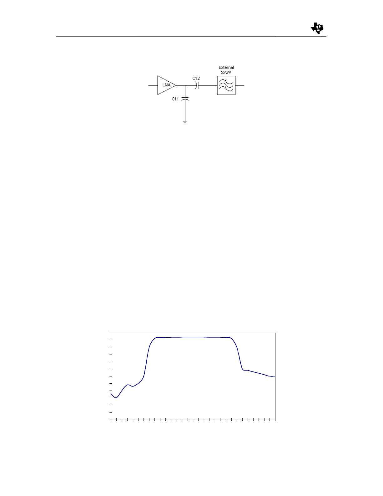
Low-B an d LNA Output
Figure 5 details the LNA output configuration. The LNA output
impedance matching network has several functions. The matching
network optimizes the third order input intercept point (IIP3)
performance while also matching the LNA output impedance to
the Surface Acoustic W a ve (SAW) filter input impedance. A
shunt-C (C11) is used to match the LNA output to the SAW filter
input. Increasing the value of the shunt capacito r will improve the
gain and noise f igu re performance but will degrade the third order
input intercept point. The end user can adjust the LNA input and
output mat chi n g network to optimize a particular parameter of
interest.
20 TRF1500 Integrat ed Dual- B and RF Receiver User’s Guide
Page 20
SWRA004A
Figure 5. Low-Band LNA Output Configuration
Surface Aco us tic Wave (SAW) Filter
The SAW filter is used primarily as an image-reject filter (IRF).
The i m age frequency (f
frequency (f
). The image frequency acts as an interferer to the system.
f
IF
) plus two times the IF frequ ency (fIF); fIM = fCH + (2 x
CH
During the down-conversion process, the image and the desired
channel are both converted to a common IF. Left unfiltered, the
image could completely mask the desired signal. The IRF rejects
this image before the RF signal is introduced to the mixer.
) is located at the desired channel
IM
By minimizing the image before it reaches the mixer, the
sensitivity of the receiver is enhanced. To further minimize
potential interferers, a band-select filter is typically used at the
front of the receiver, before the LNA. The band-select filter passes
only those frequencies that fall within the system receive band. In
many TDMA systems, the duplexor acts as the band-select filter.
The off-c hip SAW image- r eject filter used on the TR F1 500
applications board has a 3dB nominal insertion loss and a 25 MHz
bandwid th at a c en ter fr eq uency of 880 MHz as shown in Fi gur e 6.
Figure 6. SAW Filter Insertion Loss
SAW Filter Insertion Loss
0
-5
-10
-15
-20
-25
-30
-35
-40
Insertion Loss (dB)
-45
-50
-55
-60
860
Frequency (M Hz)
900
TRF1500 Integrat ed Dual- B and RF Receiver User’s Guide 21
Page 21
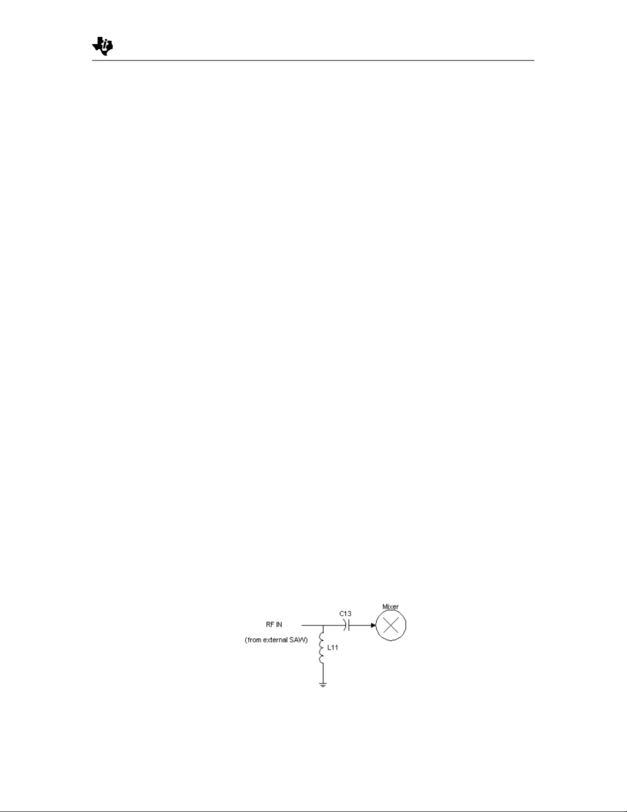
Low-Band Mixer
SWRA004A
The purpose of the mixer in a down-conversion receiver is to
translate incoming signals from one frequency to another. The
low-band mixer in the TRF1500 is a three port high-side injected
circuit. The mixer takes two known input signals, a radio frequency
(RF) signal and a local oscillator (LO) signal and mixes them
together to create a sum and difference intermediate frequency
(IF). High-side injection means the LO is higher in frequency than
the RF by the IF frequency. The output of the mixer is the IF and
contains the difference and the sum of the RF and LO signals.
The difference of the RF and LO signals is the desired IF
frequency in a down-conversion receiver. The undesired signal,
the sum of the RF and LO frequencies, can be attenuated by
using a low pass filter. The low-band mixer section of the
TRF1500 is a Gilbert cell design with open collector outputs. The
Gilbert cell structure was used for its robust isolation and
harmonic suppression characteristics.
The TRF1500 mixer typically achieves a noise figure of 7.5 dB
with an input third order intercept point of 3.5 dBm. Stand-alone
mixer performance can be ascertained by reconfiguring the
evaluati on board as noted on the dat ash eet.
Low-Band Mixe r RF Input
Figure 7 details the mixer RF input configuration. The signal from
the LNA passes through the external image-reject SAW filter and
back into the device’s low-band mixer input terminal
(MIX_IN_LOW_BAND). Minimal mixer input impedance matching
is required. A high-pass shunt-L (L11) and series-C (C13) network
are used for impedance matching the SAW filter output to the
mixer RF input. The shunt inductor presents a short at the IF
frequency. This configuration minimizes the IF leakage and
prevents unwanted interfering signals at, or near, the IF frequency
from degrading the mixer’s noise figure performance.
Figure 7. Low-Band Mixer RF Input Configuration
22 TRF1500 Integrat ed Dual- B and RF Receiver User’s Guide
Page 22
SWRA004A
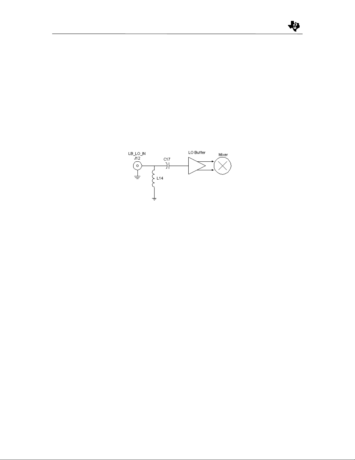
Low-Band Mixer LO Input
Figure 8 details the low-band mixer LO input configuration. The
input power range level for the LO buffer amplifier is flexible
enough (-3 dBm to -7 dBm) to drive the mixer without entering
compression. The LO signal is injected through an internal LO
buffer amplifier and into the mixer. A high pass shunt-L (L14) and
series-C (C17) network is used for impedance matching. The
inductor also shunts to ground any un desired noise that could be
injected to the mixer.
Figure 8. Low-Band Mixer LO Input Configuration
Low -Band IF Ou tput
Figure 9 details the low-band IF output configuration. The lowband mixer has a differential IF output with a 1kΩ differential
output impedance. For evaluation, a 16:1 transformer balun, with
a insertion loss of 1.8 dB, is used to transform the 1kΩ differential
output to a single-ended output which is then matched to 50Ω. In
the actual application, the IF output is usually connected to a
narrow band channel select filter with a differential input and the
transformer balun is not required.
The supply voltage (VCC) is applied to the IF pins with pull up
inductors (L12, L13). A low-pass filter network is provided prior to
the balun. The filter also acts as part of the impedance matching
network. During optimization of the output matching network, it
was found that mismatching the differential output, accomplished
with C55, gives the best IIP3 performance with minimum effect on
the gain and noi se figure performance. C5 5 als o hel ps to
decouple the digital CMOS control line from the LO signal. The IF
response is shaped by the shunt-L (L51) after the transformer
balun. L51 is also used to block unwanted noise that could be
reflect ed back to the mi xer . T he s eri es ca pac i t or (C51) ne ar t he
LB_IF_OUT port is used as a dc block for evaluation purposes
and does not have to be implemented in the end-users system.
TRF1500 Integrat ed Dual- B and RF Receiver User’s Guide 23
Page 23
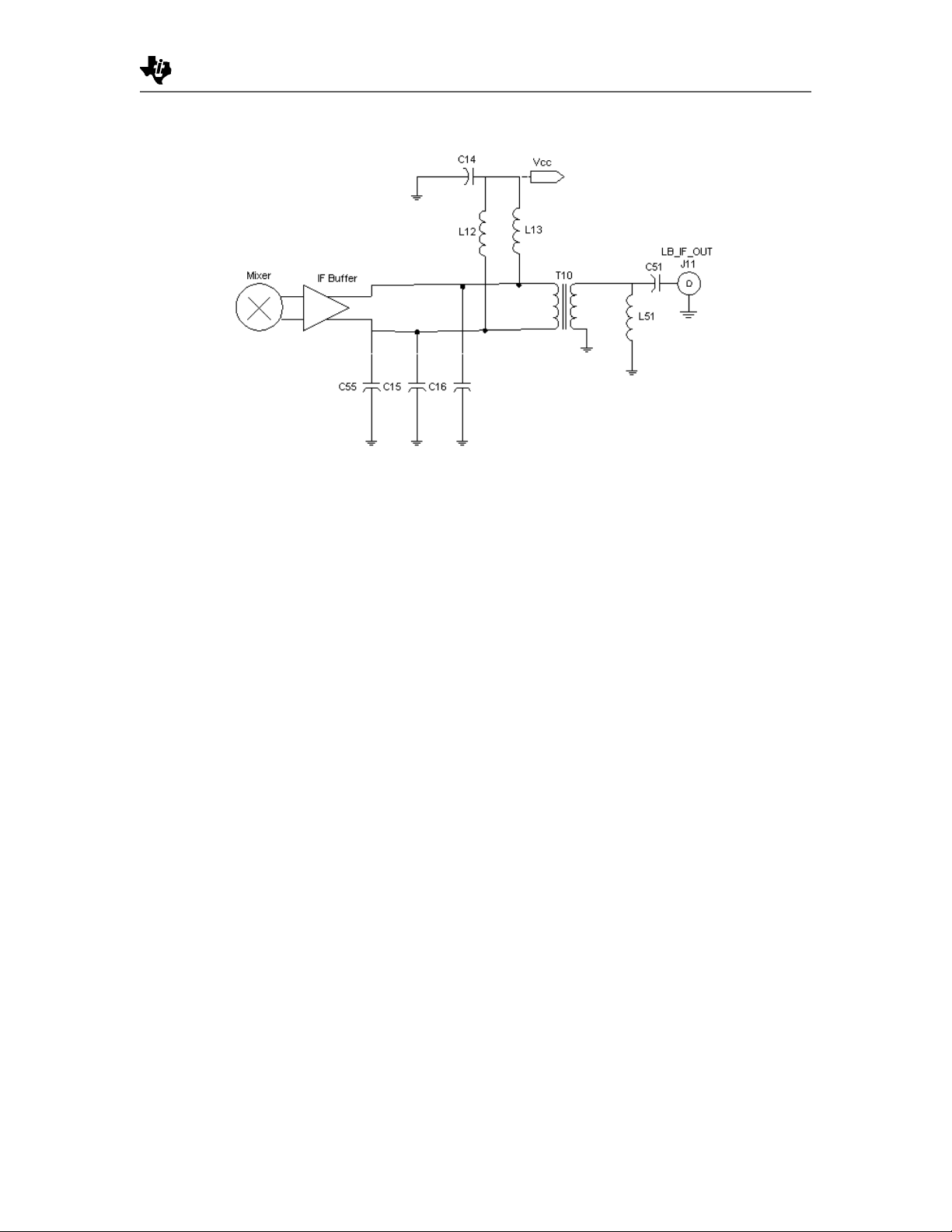
Figure 9. Low-Band IF Output Configuration
Low-B an d LO B uf fer Am pl i fie r Ou tp ut
SWRA004A
Figure 10 details the low-band LO buffer amplifier configuration.
The low-band LO buffer amplifier can be used in either singleended or differential mode for a phase lock loop (PLL)
configuration. The buffer is digitally controlled and requires a
operating drive level ranging from -3 to -7 dBm. Fo r evaluation
purposes, a 1:1 transformer balun, with an insertion loss of 2.7 dB,
is used to convert the differential output to a single-ended output.
The series capacitors at the buffer output are used for dc blocking.
The transmission line on the output of the buffer amplifier are used
to convert the 100Ω differential to 50Ω differential.
The transmission lines on the output of the buffer amplifier can be
modeled as microstrip lines. The values used for the calculations
depend on the PCB substrate, the board stackup and the required
impedance. The physical dimensions of the microstrip lines can
be calculated using standard microstrip transmission line
equations using the following values:
Frequency = 990 MHz
ER = 4.400 (FR4), Height = 12.0000 m ils , Thickness = 1.5000
mils (Copper)
Electrical Parameters:
ZO = 35.350 Ohms, E_EFF = 90.000
Physical Parameters:
Width = 37.777 mils , Length = 1613.305 mils
24 TRF1500 Integrat ed Dual- B and RF Receiver User’s Guide
Page 24

SWRA004A
Figure 10. Low-Band Buffer Amplifier Output Configuration
TRF1500 Integrat ed Dual- B and RF Receiver User’s Guide 25
Page 25

SWRA004A
Low-Band Cascaded Test Guide
This section involves measuring the cascaded performance of the
Low Band LNA, Low Band MIXER and Low Band IF Amp. An
external SAW filter is utilized to complete the RF receiver section.
All tests apply for an IF output terminated into a 1 kΩ differential
load. To match the differential IF output to the 50 Ω test
equipmen t a transformer balun is used. All unused ports are
terminated into 50 Ω.
Table 3. LB LNA, LB Mixer, SAW Filter, and LB IF Amp Parameters
PARAMETERS Min Typ Max UNIT
RF Frequency Range 869 881.5 894 MHz
LO Frequency Range 979.52 992.02 1004.52 MHz
IF Frequency 110.52 MHz
RF Input Power -30 dB m
LO Input Power -5 dBm
Power Conversi on Gain 26.0 dB
Power Conversi on Gain Reduction 19.0 dB
Noise Figure 2.5 dB
RF Input Return Loss 5.6 dB
LO Input Return Loss 16.5 dB
LO Buffer Output Power -10.3 dBm
Power Leakage LO In to RF In -53.0 dBm
Third Order Input Int er c ept Point (IIP3) -9. 7 dBm
1dB RF Input Compression Poi nt -21.0 dBm
1dB Blocking P oint -18.0 dBm
LOW-Band Cascaded: Power C onversion Gain
Control state: 011000
SEE APPENDIX A: TEST BENCH SETUPS
Test setup Figure 20
The low band power conversion gain (dB) is the measured power
(dBm) at the IF frequency minus the RF source power (dBm). It is
measured using a RF source and a spectrum analyzer.
1) Set the RF source power (RF P
(see Table 3). Connect the RF source to the EVM RF port,
J10.
26 TRF1500 Integrat ed Dual- B and RF Receiver User’s Guide
in
) and the desired frequency
Page 26

SWRA004A
2) Set the LO source power (LO Pin) and the desired frequency
(see Table 3). Connect the LO source to the EVM LO input
port, J12.
3) Set the spectrum analyzer to measure at the IF frequency (see
Table 3).
4) Connect the EVM IF output port, J11, to the spectrum
analyzer.
out
5) Measure the IF output power (IF P
) at the IF fre qu ency with
the spectrum analyzer.
6) Calculate the Cascaded Gain as:
Gain = (IF P
ou
t - RF Pin) + Transformer Loss. The
transformer loss is 1.8dB.
Example: (-5dBm - (-30dBm)) + 1.8dB = 26.8 dB.
The turn on time can be adjusted by changing the values of C10,
R6 and R7, as shown in Figure 21 and Figure 22. The resistors
form a voltage-divider network across the supply, Vcc. The
function of this network is to provide a bias condition near the
ideal operating region at the base of the common emitter amplifier.
By providing this bias condition, the charge time of the series
capacitor, C10, can be adjusted. Changing the value of resistors
should not affect gain, IIP3 or noise figure (NF) performance.
Low-Band Cascaded: Power Conversion Gain Reduction
Control state: 011010
SEE APPENDIX A: TEST BENCH SETUPS
Test setup Figure 20
The Power conversion gain reduction is the delta between the
cascaded IF Pout and the strong signal IF Pout when the strong
signal is enabled. Enabling the strong signal turns off the LNA. It is
measured using a RF source and a spectrum analyzer.
in
1) Set the RF source power (RF P
) and the desired frequency
(see Table 3). Connect the RF source to the EVM RF input
port, J10.
2) Set the LO source power (LO P
in
) and the desired frequency
(see Table 3). Connect the LO source to the EVM LO input
port, J12.
3) Set the spectrum analyzer to measure at the IF frequency (see
Table 3).
TRF1500 Integrat ed Dual- B and RF Receiver User’s Guide 27
Page 27

SWRA004A
4) Connect the EVM IF output port, J11, to the spectrum
analyzer.
out
5) Measure the output power at the IF frequency (IF P
) with the
spectrum analyzer.
6) Enable the strong signal. Measure the output power at the IF
out
frequency (SS IF P
) with the spectrum analyzer.
7) Calculate Power conversion gain reduction as:
Power Conversion Gain Reduction = (IF P
Low-Band Cascaded: Noise Figure
Control state: 011000
SEE APPENDIX A: TEST BENCH SETUPS
Test setup Figure 22
The cascaded Noise Figure (NF) is measured at the EVM Low
Band IF output port, J11. The measurement is performed using an
HP8970B Noise Figure Meter. The IF output of the mixer is
converted from differential to single ended using a transf ormer
balun. The noise figure meter requires a special setup and
calibration since the RF source and receive frequencies are
different.
Set up the nois e fi gur e met er as follows:
1) Special Function 1.4 sets the noise figure meter to measure
variabl e I F and fixed LO frequenci es.
2) The IF start, stop, and step size frequencies are set to
100MHz, 120MHz, and 5MHz respectively.
out
- SS IF P
out
).
3) Set the smoothing to 16 or above.
4) Ensure that the Excess Noise Ratio (ENR) Table on the Noise
Source head in use is entered on the NF meter.
a) On the fro nt pa nel , pre ss the EN R but to n.
b) Check the ENR value by pressing the Enter button or enter
the ENR value for each frequency.
c) After enter ing the E NR for the desired frequency, press the
Frequency button on the front panel to exit.
5) To calibrate the NF Meter:
a) Connect the Noise Source directly to the NF meter; press
the calibration twice
28 TRF1500 Integrat ed Dual- B and RF Receiver User’s Guide
Page 28

SWRA004A
b) Next, press the Noise Figure and Gain Button. The
correcte d LED jus t ab ov e the bu tton shoul d be lit.
c) Calibration is complete. Enter the desired IF frequency to
measure.
Next, the external equipment Loss is considered (RF cable,
Transmission line, filter and circulator).
6) The losses are entered in the Noise Figure Meter by using
special function 34.x.
a) Special Function 34.1 turns on the lo ss compensation
factor.
b) Special Function 34.2 is used to enter the loss before the
DUT.
c) Special Function 34.3 is used to enter the room
temperature in Kelvin (300°K).
d) Special Function 34.4 is used to enter the loss after the
DUT.
e) Special Function 34.0 is used to turn off the loss
compensation factor.
The noise fi gur e is me as ured as follows:
7) Connect the noise source directly to the EVM RF input port,
J10.
a) A circulator between the noise source and RF input port
may help minimize any mismatches between the EVM
board and t est eq ui pm e nt .
8) Connect the LO source to the EVM LO input port, J12.
a) Set the LO source at the nominal power and frequency
(See Table 3).
b) Each LO frequency being tested is entered in the Noi se
figure meter by using Special function 3.1. If the source
has excessive broad band noise, a filter at the LO port,
J12, may be necessary to eliminate the broad band noise
during testing.
9) Connect the EVM IF output port, J11, to the noise figure meter
input port.
a) A bandp ass or low pass filter m ay be ne ces sary on the IF
port to eliminate the LO signal interference and get an
accurate noise measurement.
10) Measure the Noise Figure.
TRF1500 Integrat ed Dual- B and RF Receiver User’s Guide 29
Page 29

Low-Band Cascaded: RF Input Return Loss
Control state: 011000
The input return loss of the low band receiver is measured at the
EVM low band RF input port, J10. The measurement is
performed using a network analyzer.
Set up the network analyzer as follows to measure the RF input
return loss :
1) Set the network analyzer to measure the low band RF
frequency (see Table 3).
2) Set the power range to -35 dBm th ro ugh -20 dBm, and then
set the input power to -30 dBm.
3) Perform a full one-port calibration on port 1 of the ne twork
analyzer.
4) Set the network analyzer to measure S11.
SWRA004A
5) Connect the EVM RF input, J10, to port 1 of the network
analyzer.
6) Measure the RF input retu rn loss.
Low- Band Cascaded: LO Input Return Loss
Control state: 011000
The cascaded LO input return loss of the Low Band is measured
at the EVM low band LO input port, J12. The measurement is
performed using a network analyzer.
1) Set the netwo rk analyzer to measure the low band LO
frequency (see Table 3).
2) Set the power range to -35 dBm th ro ugh -20 dBm, and then
set the input power to -30 dBm.
3) Perform a full one-port calibration on port 1 of the ne twork
analyzer.
4) Set the network analyzer to measure S11.
5) Connect the EVM LO input port, J12, to port 1 of the network
analyzer.
6) Measure the LO input return loss.
30 TRF1500 Integrat ed Dual- B and RF Receiver User’s Guide
Page 30

SWRA004A
LOW BAND: LO Buffer Output Power
Control state: 011000
SEE APPENDIX A: TEST BENCH SETUPS
Test setup Figure 20
This section involves measuring the Low Band LO Buffer Output.
All unused ports will be terminated into 50 Ω. The LO buffer output
power is measured at the EVM low band LO output port J13. A
transformer balun is used to convert the differential output to a
single ended output. The measurement is performed using a RF
source and a spectrum analyzer.
1) Set the LO source frequency and input power (see Table 3).
Connect the LO source to the EVM LO input port, J12.
2) Set the spectrum analyzer to measure at the LO frequency
(see Table 3).
3) Connect the EVM LO buffer port, J13, to the spectrum
analyzer.
4) Measure the LO buffer output power.
Low-Band: Power Leakage LO In to RF In
Control state: 011000
SEE APPENDIX A: TEST BENCH SETUPS
Test setup Figure 23
The LO leakage at the RF port is measured at the low band RF
input port J10. Power leakage is a measure of power in dBm that
couples to the RF port. The measurement is performed using a
RF source and a spectrum analyzer.
1) Set the LO source frequency and input power (see Table 3).
Connect the LO source to the EVM LO input port, J12.
2) Set the spectrum analyzer to measure at the LO frequency
(see Table 3).
3) Connect the RF Port, J10, to the spectrum analyzer.
4) Measure the LO leakage power.
TRF1500 Integrat ed Dual- B and RF Receiver User’s Guide 31
Page 31

SWRA004A
Low-Band Cascaded: Third Order Input Intercept Point (IIP3)
Control state: 011000
SEE APPENDIX A: TEST BENCH SETUPS
Test setup Figure 21:
The third order input intercept point is the level of the RF input
power at which the output power levels of the undesired
intermodulation products and the desired IF products are equal.
The measurement is performed using three RF sources and a
spectrum analyzer.
1) Set the first RF source input power (RF P
in
) and frequency (F1)
(see Table 3).
2) Set the second RF source frequency to the first RF frequency
plus 60kHz; F
.
2
3) Using a RF combiner, connect the RF sources to the EVM RF
input port, J10.
4) Set the LO source frequency and input power (see Table 3).
Connect the LO source to the EVM LO input port, J12.
5) Set the spectrum analyzer to measure at the IF frequency (F
IF
(see Table 3).
6) Connect the EVM IF output port, J11 to the spectrum analyzer.
7) Measure the Fundamental output power at the IF frequency
Fund
).
(F
8) Measure the Intermodulation products (2F2 - F1 or 2F1 - F2) at
IF
F
60 kHz
±
9) Calculate the Intermodulation Suppression as:
Fund
Intermodulation Suppression = F
- Intermodulation
product
)
10) Calculate the Input Third -Order Intercept Point as:
Input Third-Orde r Intercept = ((Intermodulation
Suppress ion/2) + (RF P
32 TRF1500 Integrat ed Dual- B and RF Receiver User’s Guide
))
in
Page 32

SWRA004A
Low-Band Cascaded: 1dB RF Input Compression Point
Control state: 011000
SEE APPENDIX A: TEST BENCH SETUPS
Test setup Figure 20
The 1 dB input compressio n point is the RF input power at which
the gain compre sses 1 dB. Gain compression is when an increase
in
in P
causes no further increase in the output power (P
measurement is performed using two RF sources and a spectrum
analyzer.
1) Set the RF source frequency (see Table 3) and the input
power (P
input port, J10.
2) Set the LO source frequency and input power (see Table 3).
Connect the LO source to the EVM LO input port, J12.
3) Set the spectrum analyzer to measure the output power at the
IF frequency.
in
) to -35 dBm. Connect the RF source to the EVM RF
out
). The
4) Connect the EVM IF output port, J11, to the spectrum
analyzer.
5) Measure the output power (P
6) Calculate Gain as:
out
in
Gain = P
- P
7) To determine the 1 dB compression point, the RF P
increased in steps of 1 dBm unti l the gain compresses by 1
dB. Repeat step 4 and 5 until th e gain compre sses by 1dB.
in
RF P
-35 -10 25
-34 -9 25
-33 -8 25
-32 -7 25
-31 -6 25
-30 -5 25
-29 -4 25
-28 -3 25
-27 -2 25
-26 -1.2 24.8
-25 -0.4 24.6
out
P
Gain
out
) at the IF freq u ency
in
is
TRF1500 Integrat ed Dual- B and RF Receiver User’s Guide 33
Page 33

-24 0.4 24.4
-23 1.2 24.2
-22 2.2 24.2
-21 3.0
-20 3.0 23.0
24.0 ←1dB Compression Point
Low-Band Cascaded: 1dB Blocking Point
Control state: 011000
SEE APPENDIX A: TEST BENCH SETUPS
Test setup Figure 21
The 1dB Blocking Point is a measurement of the power (dBm) of
the interfering signal, measured at the EVM IF output port J11.
The measurement is performed using three sources and a
spectrum analyzer.
1) Set the RF source frequency and input power (see Table 3).
SWRA004A
2) Set the RF Blocking source freq ue nc y to t he RF fre qu ency
minus 45 MHz at -30dBm input power.
3) Using a RF combiner, connect the RF sources to the EVM RF
port, J10.
4) Set the LO source frequency and input power (see Table 3).
Connect the LO source to the EVM LO input port, J12.
5) Set the spectrum analyzer to measure the output power at the
IF frequency.
6) Connect the EVM IF port, J11, to the spectrum analyzer.
7) To determine the 1dB Blocking Point, increase the RF
Blocking source input power until the output power at the IF
freque ncy is decreased by 1dB.
8) Disconnect the Blocking source.
9) Connect the Blocking source directly to the spectrum analyzer,
and change the spectrum analyzer’s frequency to the
frequency of the Blocking source.
10) Measure the power of the Blocking source.
34 TRF1500 Integrat ed Dual- B and RF Receiver User’s Guide
Page 34

SWRA004A
High-Band Cascaded Receiver Section: LNA, Mixer, LO
Buffer Ampli fi er
Cascaded High-Band Receiver Section:
The TRF1500 high-band receiver section, shown in Figure 11, is
an integrated front-end down converter designed to operate in the
1900 MHz frequency ra nge. The high-band down converter
consists of an LNA, an image-reject mixer, and LO buffer amplifier
circuitry. Figure 11 details the cascaded block diagram with the
image reject mixer detailed inside the dotted box.
The digital control allows the high-band receiver to operate in
three different states to compensate for the environment in which
the TRF1500 is operating. The high-band receiver can be
operated in the normal state, where the LNA, mixer and buffer
amplifier are on, the strong signal state, where the LNA is off and
the mixer and buffer amplifier are on, or the transmit state, where
the LNA bias current is increased to prevent compression when
the transmitter is on.
The high- ba nd rec ei v er has a ty pi cal nominal gain of 26 dB , an
IIP3 of -17.7 dBm and a noise figure of 4.66 dB when the receiver
LO doubler is used and 4.35 dB when the high-band LO is directly
driven.
LNA, Mixer, and LO Amplifier
Figure 11. Block Diagram of the High-Band Receiver Section
TRF1500 Integrat ed Dual- B and RF Receiver User’s Guide 35
Page 35

High-Band RF Input
Figure 12 details the high-band RF input configuration. The
cascaded noise figure and input return loss performance of the
high-band receiver section is determined primarily by the input
matching network. The input matching network is designed for
optimum noise figure performance, while maintaining good input
return loss. A lo w-pass shunt-C (C20) series-L (L20) network is
used for the input impedance matching. The series capacitor
(C29) on the input port is used for dc blocking purposes. The enduser can optimize the input matching network for better input
return loss but obtaining a be tter input match may degrade the
overall c ascaded noise figure per form a nce.
Figure 12. High-Band RF Input Configuration
SWRA004A
High-B an d LO I n pu t
The high-band LO signal is fed through a buffer amplifier into a
differential quadrature generator, which is realized using a
polyphase network. The signals generated by the polyphase
network are used to drive two mixers which are injected with a
common RF signal. The IF signals out of these mixers will have a
180° phase shift of the image frequency as compared to the
wanted RF frequency. As a result of this 180° phase shift, the IF
signals at the image frequency will cancel in the quadrature
combiner. The IF signal at the desired frequency will add in the
quadrature combiner.
The TRF1500 offers several methods for providing high-band LO
drive. The high-band LO terminal may be directly driven either
single-ended or differentially. Alternately, the high-band LO
terminal may be driven by using the low-band LO output and the
integrat ed fr equency doubler.
36 TRF1500 Integrat ed Dual- B and RF Receiver User’s Guide
Page 36

SWRA004A
Figure 13 details the TRF1500 configured to utilize the low-ban d
LO input and doubler as the high-band LO. The high-band LO
signal is injected into the low-band LO input. The buffered signal
is then routed through the doubler. The output of the doubler is
routed through an external capacitor (C40) and into the singleended high-band LO input.
Figure 14 details the TRF1500 configured to utilize the high -band
LO. The signal is directly injected into the high-band LO input
which dir ectl y dr iv es the high-b and down converter.
Note:
L40, and change the value of C41 to 1pF and populate
C24.
To use the high-band LO input, remove C40 and
Figure 13. High-Band LO Frequency Doubler Driven Configuration
Figure 14. High-Band LO Directly Driven Configuration
TRF1500 Integrat ed Dual- B and RF Receiver User’s Guide 37
Page 37

High-Band IF Output
Figure 15 details the high-band mixer IF output configuration. The
high-band mixer has a differential IF output with a 1kΩ differen ti al
output impedance. For evaluation purposes, a 16:1 transformer
balun, with an insertion loss of 1.8 dB, is used to transform the
1kΩ differential output to a single-ended output which is then
matched to 50Ω. In the actual application, the IF output is usually
connected to a narrow band channel select filter with a differential
input and the transformer balun is not required.
The supply voltage (VCC) is applied to the IF terminals with pullup inductors (L21, L22). A low-pass filter network is provided prior
to the balun. The filter also acts as part of the impedance
matching network. The IF response is shaped by the shunt-L
(L52) after the transformer balun. L52 is also used to block
unwanted noise that could be reflected back to the mixer. The
series capacitor (C51) near the HB_IF_OUT port is used as a dc
block for evaluation purpos es an d does not have to be
implemented in the end-users system.
SWRA004A
Figure 15. High-Band IF Output Configuration
38 TRF1500 Integrat ed Dual- B and RF Receiver User’s Guide
Page 38

SWRA004A
High-B an d LO B uf fer Am plifier Ou tpu t
Figure 16 details the high-band LO buffer amplifier configuration.
The high-band LO buffer can be used in either single-ended or
differential mode for a phase lock loop (PLL) configuration. The
buffer is digitally controlled and requires an operating drive level
ranging from -3 to -7dBm. For evaluation purposes, a 1:1
transformer balun, with an insertion loss of 2.7 dB, is used to
convert the differential output to a single-ended output. The series
capacitors at the buffer output are for dc blocking.
The transmission line on the output of the buffer amplifier are used
to convert the 100Ω differential to 50Ω differential.
The transmission lines on the output of the buffer amplifier can be
modeled as microstrip lines. The values used for the calculations
depend on the PCB substrate, the board stackup and the required
impedance. The physical dimensions of the microstip lines can be
calculated with standard transmission line equations using the
following values:
The following information are used to calculate the microstrip
transmission lines:
Frequency = 2.070 GHz
ER = 4.400 (FR4), Height = 12.0000 mils, Thickness = 1.5000 mils
(Copper)
Electrical Parameters:
ZO = 35.350, E_EFF = 90 .000
Results:
Physical Parameters:
Width = 37.777, Length = 771.149
Figure 16. High-Band LO Buffer Amplifier Output Configuration
TRF1500 Integrat ed Dual- B and RF Receiver User’s Guide 39
Page 39

SWRA004A
High-Band Cascaded Test Guide
This section involves measuring the cascaded performance of the
High Band LNA, High Ba nd Mixer and High Band IF Amp using
the Frequency Doubler. All tests apply for an IF output terminated
into a 1 kΩ differential load. A transformer balun is used to match
the IF output to the 50 Ω test equipment. All unused ports are
terminated into 50 Ω.
Table 4. HB LNA, HB mixer, HB IF amp
PARAMETERS Min Typ Max UNIT
RF Input Frequency Range 1930 1960 1990 MHz
Direct Drive LO Frequency Range 2040.52 2070.52 2100.52 MHz
Doubler Driv e LO Frequenc y Range 1020.26 1035. 26 1050.26 MHz
IF Frequency 110.52 MHz
RF Input Power -30 dBm
LO Input Power -5 dBm
Power Conversi on Gain 26.3 dB
Power Conversi on Gain Reduction 43.5 dB
Image Rejecti on 22.5 dB
Noise Figure 4.66 dB
RF Input Return Loss 14.2 dB
LO Buffer Output Power -14 dB m
Power Leakage LO In to RF In -50 dBm
Third Order Input Intercept Point(IIP3) -17.7 dBm
1dB RF Input Compression Poi nt -23.7 dBm
2X2 Spur Performance 69 dBc
3X3 Spur Performance 81 dBc
High-Ban d C asc a de d: Pow er Con ver sion Gain
Control state: 111001
SEE APPENDIX A: TEST BENCH SETUPS
Test setup Figure 20
The high band power conversion gain (dB) is the measured power
(dBm) at the IF frequency minus the RF source power (dBm). It is
measured using a RF source and a spectrum analyzer.
1) Set the RF source power (RF P
(see Table 4). Connect the RF source to the EVM RF port,
J20.
40 TRF1500 Integrat ed Dual- B and RF Receiver User’s Guide
in
) and the desired frequency
Page 40

SWRA004A
2) Set the LO source power (LO Pin) and the desired frequency
(see Table 4). Connect the LO source to the EVM LO input
port, J12.
3) Set the spectrum analyzer to measure at the IF frequency (see
Table 4).
4) Connect the EVM IF output port, J21, to the spectrum
analyzer.
out
5) Measure the IF output power (IF P
) at the IF fre qu ency with
the spectrum analyzer.
6) Calculate the Cascaded Gain as:
Gain = (IF P
out
- RF Pin) + Transformer Loss. The
transformer loss is 1.8dB.
High-B an d Casc a de d: Pow er Con ver sion Gain Re du cti on
Control state: 111011
SEE APPENDIX A: TEST BENCH SETUPS
Test setup Figure 20
The Power conversion gain reduction is the delta between the
cascaded IF Pout and the strong signal IF Pout when the strong
signal is enabled. Enabling the strong signal turns off the LNA. It is
measured using a RF source and a spectrum analyzer.
1) Set the RF source power (RF P
(see Table 4). Connect the RF source to the EVM RF input
port, J20.
2) Set the LO source power (LO P
(see Table 4). Connect the LO source to the EVM LO input
port, J12.
3) Set the spectrum analyzer to measure at the IF frequency (see
Table 4).
in
) and the desired frequency
in
) and the desired frequency
4) Connect the EVM IF output port, J21, to the spectrum
analyzer.
out
5) Measure the output power at the IF frequency (IF P
) with the
spectrum analyzer.
6) Enable the strong signal. Measure the output power at the IF
out
frequency (SS IF P
) with the spectrum analyzer.
7) Calculate Power conversion gain reduction as:
out
Power Conversion Gain Reduction = (IF P
- SS IF P
TRF1500 Integrat ed Dual- B and RF Receiver User’s Guide 41
out
).
Page 41

High-Band Cascaded: Image Rejection
Control state: 111001
SEE APPENDIX A: TEST BENCH SETUPS
Test setup Figure 20
Image Rejection is a signal that appears at twice the IF distance
from the desired RF signal, located on the opposite side of the LO
frequency from the desired RF signal. The measurement is
performed using two RF sources and a spectrum analyzer.
SWRA004A
1) Set the RF source power (RF P
frequency (F
RF
) (see Table 4). Connect the RF source to the
in
) and the desi r ed RF
EVM RF input port, J20.
in
2) Set the LO source power (LO P
frequency (F
LO
)(see Table 4). Connect the LO source to the
) and the desi r ed LO
EVM LO input port, J12.
3) Set the spectrum analyzer to measure at the IF frequency
IF
(F
)(see Table 4).
4) Connect the EVM IF output port, J21, to the spectrum
analyzer.
out
5) Measure the output power at the IF frequency (IF P
) with the
spectrum analyzer.
6) Set the RF Frequency to F
RF
7) Measure the output power at the IF frequency (IF P
+ 2 F
IF.
out
) with the
spectrum analyzer
8) Calculate the Image Rejection as
Image Rejection = ∆ between the IF output power at ( F
and the IF output power at F
RF
+ 2 F
IF
RF
)
42 TRF1500 Integrat ed Dual- B and RF Receiver User’s Guide
Page 42

SWRA004A
High-Band Cascaded: Noise Figure
Control state: 111001
SEE APPENDIX A: TEST BENCH SETUPS
Test setup Figure 22
The cascaded Noise Figure (NF) is measured at the EVM Low
Band IF output port, J21. The measurement is performed using an
HP8970B Noise Figure Meter. The IF output of the mixer is
converted from differential to single ended using a transf ormer
balun. The noise figure meter requires a special setup and
calibration since the RF source and receive frequencies are
different.
Set up the nois e fi gur e met er as follows:
1) Special Function 1.4 sets the noise figure meter to measure
variabl e I F and fixed LO frequenci es.
2) The IF start, stop, and step size frequencies are set to
100MHz, 120MHz, and 5MHz respectively.
3) Set the smoothing to 16 or above.
4) Ensure that the Excess Noise Ratio (ENR) Table on the Noise
Source head in use is entered on the NF meter.
a) On the fro nt pa nel , pre ss the EN R but to n.
b) Check the ENR value by pressing the Enter button or enter
the ENR value for each frequency.
c) After enter ing the E NR for the desired frequency, press the
Frequency button on the front panel to exit.
5) To calibrate the NF Meter:
a) Connect the Noise Source directly to the NF meter; press
the calibration button twice.
b) Next, press the Noise Figure and Gain Button. The
correcte d LED jus t ab ov e the bu tton shoul d be lit.
c) Calibration is complete. Enter the desired IF frequency to
measure.
Next, the external equipment Loss is considered (RF cable,
Transmission line, filter and circulator).
6) The losses are entered in the Noise Figure Meter by using
special function 34.x.
TRF1500 Integrat ed Dual- B and RF Receiver User’s Guide 43
Page 43

SWRA004A
a) Special Function 34.1 turns on the lo ss compensation
factor.
b) Special Function 34.2 is used to enter the loss before the
DUT.
c) Special Function 34.3 is used to enter the room
temperature in Kelvin (300°K).
d) Special Function 34.4 is used to enter the loss after the
DUT.
e) Special Function 34.0 is used to turn off the loss
compensation factor.
The noise fi gur e is me as ured as follows:
7) Connect the noise source directly to the EVM RF input port,
J20.
a) A circulator between the noise source and RF input port
may help minimize any mismatches between the EVM
board and t est eq ui pm e nt .
8) Connect the LO source to the EVM LO input port, J12.
a) Set the LO source at the nominal power and frequency
(See Table 4).
b) Each LO frequency being tested is entered in the Noi se
figure meter by using Special function 3.1. If the source
has excessive broad band noise, a filter at the LO port,
J12, may be necessary to eliminate the broad band noise
during testing.
9) Connect the EVM IF output port, J21, to the noise figure meter
input port.
a) A bandp ass or low pass filter m ay be ne ces sary on the IF
port to eliminate the LO signal interference and get an
accurate noise measurement.
10) Measure the Noise Figure.
High-Band Cascaded: RF Input Return Loss
Control state: 111001
The cascaded input return loss of the high band is measured at
the high band RF input port, J20. The measurement is performed
using a network analyzer.
Set up the network analyzer as follows to measure the RF input
return loss :
44 TRF1500 Integrat ed Dual- B and RF Receiver User’s Guide
Page 44

SWRA004A
1) Set the network analyzer to measure the low band RF
frequency (see Table 4).
2) Set the power range to -35 dBm th ro ugh -20 dBm, and then
set the input power to -30 dBm.
3) Perform a full one-port calibration on port 1 of the ne twork
analyzer.
4) Set the network analyzer to measure S11.
5) Connect the EVM RF input, J20, to port 1 of the network
analyzer.
6) Measure the RF input retu rn loss.
High-Band: LO Buffer Output Power
Control state: 111001
SEE APPENDIX A: TEST BENCH SETUPS
Test setup Figure 20
This section involves measuring the Low Band LO Buffer Output.
All unused ports will be terminated into 50 Ω. The LO buffer output
power is measured at the EVM low band LO output port J23. A
transformer balun is used to convert the differential output to a
single ended output. The measurement is performed using a RF
source and a spectrum analyzer.
1) Set the LO source frequency and input power (see Table 4).
Connect the LO source to the EVM LO input port, J12.
2) Set the spectrum analyzer to measure at the LO frequency
(see Table 4).
3) Connect the EVM LO buffer port, J23, to the spectrum
analyzer.
4) Measure the LO buffer output power.
TRF1500 Integrat ed Dual- B and RF Receiver User’s Guide 45
Page 45

High-Band Cascaded: Power Leakage LO In to RF In
Control state: 111001
SEE APPENDIX A: TEST BENCH SETUPS
Test setup Figure 23
The LO leakage at the RF port is measured at the low band RF
input port J20. Power leakage is a measure of power in dBm that
couples to the RF port. The measurement is performed using a
RF source and a spectrum analyzer.
1) Set the LO source frequency and input power (see Table 4).
Connect the LO source to the EVM LO input port, J12.
2) Set the spectrum analyzer to measure at the LO frequency
(see Table 4).
3) Connect the RF Port, J20, to the spectrum analyzer.
4) Measure the LO leakage power.
SWRA004A
High-Band Cascaded: Third Order Input Intercept Point (IIP3)
Control state: 111001
SEE APPENDIX A: TEST BENCH SETUPS
Test setup Figure 21
The third order input intercept point is the level of the RF input
power at which the output power levels of the undesired
intermodulation products and the desired IF products are equal.
The measurement is performed using three RF sources and a
spectrum analyzer.
1) Set the first RF source input power (RF P
(see Table 4).
2) Set the second RF source frequency to the first RF frequency
plus 120kHz; F
.
2
3) Using a RF combiner, connect the RF sources to the EVM RF
input port, J20.
4) Set the LO source frequency and input power (see Table 4).
Connect the LO source to the EVM LO input port, J12.
in
) and frequency (F1)
5) Set the spectrum analyzer to measure at the IF frequency (F
IF
(see Table 4).
46 TRF1500 Integrat ed Dual- B and RF Receiver User’s Guide
)
Page 46

SWRA004A
6) Connect the EVM IF output port, J21 to the spectrum analyzer.
7) Measure the Fundamental output power at the IF frequency
Fund
).
(F
8) Measure the Intermodulation products (2F
IF
120 kHz
F
±
2
- F1 or 2F1 - F2) at
9) Calculate the Intermodulation Suppression as:
Fund
Intermodulation Suppression = F
- Intermodulation
product
10) Calculate the Input Third -Order Intercept Point as:
Input Third-Orde r Intercept = ((Intermodulation
Suppress ion/2) + (RF P
))
in
High-Band Cascaded: 1dB Input Compress ion Point
Control state: 111001
SEE APPENDIX A: TEST BENCH SETUPS
Test setup Figure 20
The 1 dB input compressio n point is the RF input power at which
the gain compre sses 1 dB. Gain compression is when an increase
in
in P
causes no further increase in the output power (P
measurement is performed using two RF sources and a spectrum
analyzer.
out
). The
1) Set the RF source frequency (see Table 4) and the input
in
power (P
) to -35 dBm. Connect the RF source to the EVM RF
input port, J20.
2) Set the LO source frequency and input power (see Table 4).
Connect the LO source to the EVM LO input port, J12.
3) Set the spectrum analyzer to measure the output power at the
IF frequency.
4) Connect the EVM IF output port, J21, to the spectrum
analyzer.
out
5) Measure the output power (P
) at the IF freq u ency
6) Calculate Gain as:
out
in
Gain = P
7) To determine the 1 dB compression point, the RF P
- P
in
is
increased in steps of 1 dBm unti l the gain compresses by 1
dB. Repeat step 4 and 5 until th e gain compre sses by 1dB.
TRF1500 Integrat ed Dual- B and RF Receiver User’s Guide 47
Page 47

SWRA004A
RF P
in
out
P
Gain
-35 -10 25
-34 -9 25
-33 -8 25
-32 -7 25
-31 -6 25
-30 -5 25
-29 -4 25
-28 -3 25
-27 -2 25
-26 -1.2 24.8
-25 -0.4 24.6
-24 0.4 24.4
-23 1.2 24.2
-22 2.2 24.2
-21 3.0
24.0 ←1dB Compression Point
-20 3.0 23.0
High-Band Cascaded: 2X2 Spur Performance
Control state: 111001
SEE APPENDIX A: TEST BENCH SETUPS
Test setup Figure 20
2X2 Spur Performance is measured at IF output port J21. The
measurement is performed using two sources and a spectrum
analyzer.
1) Set the RF source frequency (F
RF)
and input power (see Table
4). Connect the RF source to the EVM RF input port, J20.
2) Set the LO source frequency and input power (see Table 4).
Connect the LO source to the EVM LO input port, J12.
3) Set the spectrum analyzer to measure the output power at the
IF frequency; F
IF
4) Connect the EVM IF output port, J21, to the spectrum
analyzer.
out
5) Measure the output power (1 P
6) Set the RF source Frequency to (F
) at the IF freq uen cy .
RF
+ ½ FIF) and Pin to -
50dBm.
out
7) Measure the output power (2 P
) at the IF freq uen cy .
48 TRF1500 Integrat ed Dual- B and RF Receiver User’s Guide
Page 48

SWRA004A
8) Calculate 2 X 2 spur performance as 2 X 2 spur performance
= 1 P
out
- 2 P
out.
High Band: 3X3 Spur Performance
Control state: 111001
SEE APPENDIX A: TEST BENCH SETUPS
Test setup Figure 20
3X3 Spur Performance is measured at IF output port J21. The
measurement is performed using two sources and a spectrum
analyzer.
1) Set the RF source frequency (F
RF)
and input power (see Table
4). Connect the RF source to the EVM RF input port, J20.
2) Set the LO source frequency and input power (see Table 4).
Connect the LO source to the EVM LO input port, J12.
3) Set the spectrum analyzer to measure the output power at the
IF frequency; F
.
IF
4) Connect the EVM IF output port, J21, to the spectrum
analyzer.
out
5) Measure the output power (1 P
6) Set the RF source Frequency to (F
) at the IF freq uen cy .
RF
+ 2/3 FIF) and the source
power to -50dBm.
out
7) Measure the output power (2 P
) at the IF freq uen cy .
8) Calculate 3 x 3 spur per for m ance as:
3 x 3 spur performance = 1 P
out
- 2 P
out.
TRF1500 Integrat ed Dual- B and RF Receiver User’s Guide 49
Page 49

Low-Band and High-Ba nd Transmit
Low- and High-Band Transmit Mixer
Figure 17 details the block diagram of the transmit mixer. The
TRF1500 provides a transmit mixer for down converting the
system transmit signal (low-band or high-band) to a common IF
for loop-back testing. The LO input for this mixer can be selected
from either the low-band LO input or the high-band LO input by
means of the digital control. The RF input of the transmit mixer
provides a broad-band 200Ω differential input impedance over a
band of 800 MHz to 2GHz and thus requires minimal external
matching.
The mixer is a double-balanced G ilbert cell design with open
collector outputs. The Gilbert cell structure was implemented for
its robust isolation and harmonic suppression characteristics.
Figure 17. Transmit Mixer Block Diagram
SWRA004A
Low-Band and High-Band Transmit Mixer RF Input
Figure 18 details the transmit mixer RF input configuration. The
transmit mixer can be either driven single-ended or differentially.
For evaluation purposes, a 4:1 transformer balun is used on the
EVM to drive the transmit mixer single-ended. The input requires
very little external matching. A shunt capacitor (C35) near the
input port (J30) and a shunt capacitor (C36) near the transformer
balun (T30) are the only input impedance matching components
required.
50 TRF1500 Integrat ed Dual- B and RF Receiver User’s Guide
Page 50

SWRA004A
Figure 18. Low- and High-Band Transmit Mixer RF Input Configuration
Low- and High-Band Transmit Mixer IF Output
Figure 19 details the transmit mixer IF output configuration. The
transmit mixer has a differential IF output with a 1kΩ differen ti al
impedance. For evaluation purposes, a 16:1 transformer balun,
with an insertion loss of 1.8 dB, is used to transform the 1k
differential output to a single-ended output which is then matched
to 50Ω.
Ω
The supply voltage (VCC) is applied to the IF pins with pull up
inductors (L30, L31). A low-pass filter network is provided prior to
the balun. This filter also acts as part of the impedance matching
network. The IF response is shaped by the shunt inductor (L50)
after the transformer balun. L50 is also used to block unwanted
noise that could be reflected back to the mixer. The series
capacitor (C50), near the TX_IF_OUT port, is used as a dc block
for evaluation purposes and does not have to be implemented in
the end-users system.
Figure 19. Low- and High-Band Transmit Mixer IF Output Configuration
TRF1500 Integrat ed Dual- B and RF Receiver User’s Guide 51
Page 51

SWRA004A
Low-Band Transmit M ixer Test Guide
This section involves measuring the Transmit Mixer perf ormance.
All tests apply for an IF output terminated into a 1 kΩ differential
load. To match the IF output to the 50 Ω test equipment a
transformer balun is used. All unused ports are terminated into 50
.
Ω
Table 5. Low-Band Transmit Performance Parameters
PARAMETERS Min Typ Max UNIT
Tx Mixer Input Frequenc y Range 824 836. 5 849 MHz
LO Input Frequency Range 941 953. 5 966 MHz
Tx Mixer IF Frequency 117 MHz
RF Input Power -30 dBm
LO Input Power -5 dBm
Power Conversi on Gain 19 dB
Noise Figure 7.8 dB
Input Return Loss 9.8 dB
Power Leakage LO In to Tx In -49 dB
Power Leakage Tx I n to LO In -70.6 dB
1dB Input Compression Point -20 dBm
Second Order Input intercept Point (IIP2) 29.5 dBm
Third Order Input Intercept Point(IIP3) -11.5 dBm
Low-Band Transmit Mixer: Power Conversion Gain
Control state: 010100
SEE APPENDIX A: TEST BENCH SETUPS
Test setup Figure 20
The low band transmit mixer power conversion gain (dB) is the
measured power (dBm) at the IF frequency minus the RF source
power (dBm). It is measured using a RF source and a spectrum
analyzer.
in
1) Set the RF source power (RF P
(see Table 5). Connect the RF source to the EVM RF port,
J30.
2) Set the LO source power (LO P
(see Table 5). Connect the LO source to the EVM LO input
port, J12.
52 TRF1500 Integrat ed Dual- B and RF Receiver User’s Guide
) and the desired frequency
) and the desired frequency
in
Page 52

SWRA004A
3) Set the spectrum analyzer to measure at the IF frequency (see
Table 5).
4) Connect the EVM IF output port, J31, to the spectrum
analyzer.
5) Measure the IF output power (IF P
the spectrum analyzer.
6) Calculate the Cascaded Gain as:
out
Gain = (IF P
- RF Pin) + Transformer Loss. The
transformer loss is 1.8dB.
Low-Band Transmit Mixer: Noise Figure
Control state: 010100
SEE APPENDIX A: TEST BENCH SETUPS
Test setup Figure 22
The cascaded Noise Figure (NF) is measured at the EVM Low
Band IF output port, J31. The measurement is performed using an
HP8970B Noise Figure Meter. The IF output of the mixer is
converted from differential to single ended using a transf ormer
balun. The noise figure meter requires a special setup and
calibration since the RF source and receive frequencies are
different.
out
) at the IF fre qu ency with
Set up the nois e fi gur e met er as follows:
1) Special Function 1.4 sets the noise figure meter to measure
variabl e I F and fixed LO frequenci es.
2) The IF start, stop, and step size frequencies are set to
114MHz, 120MHz, and 3MHz respectively.
3) Set the smoothing to 16 or above.
4) Ensure that the Excess Noise Ratio (ENR) Table on the Noise
Source head in use is entered on the NF meter.
a) On the fro nt pa nel , pre ss the EN R but to n.
b) Check the ENR value by pressing the Enter button or enter
the ENR value for each frequency.
c) After enter ing the E NR for the desired frequency, press the
Frequency button on the front panel to exit.
5) To calibrate the NF Meter:
a) Connect the Noise Source directly to the NF meter; press
the calibration button twice.
TRF1500 Integrat ed Dual- B and RF Receiver User’s Guide 53
Page 53

SWRA004A
b) Next, press the Noise Figure and Gain Button. The
correcte d LED jus t ab ov e the bu tton shoul d be lit.
c) Calibration is complete. Enter the desired IF frequency to
measure.
Next, the external equipment Loss is considered (RF cable,
Transmission line, filter and circulator).
6) The losses are entered in the Noise Figure Meter by using
special function 34.x.
a) Special Function 34.1 turns on the lo ss compensation
factor.
b) Special Function 34.2 is used to enter the loss before the
DUT.
c) Special Function 34.3 is used to enter the room
temperature in Kelvin (300°K).
d) Special Function 34.4 is used to enter the loss after the
DUT.
e) Special Function 34.0 is used to turn off the loss
compensation factor.
The noise fi gur e is me as ured as follows:
7) Connect the noise source directly to the EVM RF input port,
J30.
8) Connect the LO source to the EVM LO input port, J12.
a) Set the LO source at the nominal power and frequency
(See Table 5).
b) Each LO frequency being tested is entered in the Noi se
figure meter by using Special function 3.1.
9) Connect the EVM IF output port, J31, to the noise figure meter
input port.
10) Measure the Noise Figure.
Low-Band Transmit Mixer: Input Return Loss
Control state: 010100
The cascaded input return loss of the low band transmit mixer is
measured at the EVM low band RF input port, J30. The
measurement is performed using a network analyzer.
Set up the network analyzer as follows to measure the RF input
return loss :
54 TRF1500 Integrat ed Dual- B and RF Receiver User’s Guide
Page 54

SWRA004A
1) Set the network analyzer to measure the low band RF
frequency (see Table 5).
2) Set the power range to -35 dBm th ro ugh -20 dBm, and then
set the input power to -30 dBm.
3) Perform a full one-port calibration on port 1 of the ne twork
analyzer.
4) Set the network analyzer to measure S11.
5) Connect the EVM RF input, J30, to port 1 of the network
analyzer.
6) Measure the RF input retu rn loss.
Low-Band Transmit Mixer: Power Leakage LO In to TX In
Control state: 010100
SEE APPENDIX A: TEST BENCH SETUPS
Test setup Figure 23
The LO In leakage at the TX In port is measured at the low band
TX input port J30. Power leakage is a measure of power (in dBm)
that couples to the TX port. The measurement is performed using
a RF source and a spectrum analyzer.
1) Set the LO source frequency and input power (see Table 5).
Connect the LO source to the EVM LO input port, J12.
2) Set the spectrum analyzer to measure at the LO frequency
(see Table 5).
3) Connect the TX In Port, J30, to the spectrum analyzer.
4) Measure the LO leakage power.
Low-Band Transmit Mixer: Power Leakage TX In to LO In
Control state: 010100
SEE APPENDIX A: TEST BENCH SETUP
Test setup Figure 24
The Power leakage from TX IN to LO IN is measured at the LO in
port, J12. A leakage is a measure of power (in dBm) that couples
to the LO IN port. The measurement is performed using a RF
source and a spectrum analyzer.
TRF1500 Integrat ed Dual- B and RF Receiver User’s Guide 55
Page 55

1) Set the TX source frequency and input power (see Table 5).
Connect the TX source to the EVM TX input port, J30.
2) Set the spectrum analyzer to measure at the T X frequency
(see Table 5).
3) Connect the LO In Port, J12, to the spectrum analyzer.
4) Measure the TX leakage power.
Low-Ban d Tran sm it Mixer : 1dB Inp ut Compressi on Point
Control state: 010100
SEE APPENDIX A: TEST BENCH SETUPS
Test setup Figure 20
The 1 dB input compression point is the TX RF input power at
which the gain compresses 1 dB. Gain compressio n is when an
in
increase in P
out
). The measurement is performed using two RF sources and a
(P
spectrum analyzer.
causes no further increase in the output power
SWRA004A
1) Set the TX RF source frequency (see Table 5) and the input
power (P
in
) to -35 dBm. Connect the RF source to the EVM RF
input port, J30.
2) Set the LO source frequency and input power (see Table 5).
Connect the LO source to the EVM LO input port, J12.
3) Set the spectrum analyzer to measure the output power at the
IF frequency.
4) Connect The EVM TX IF output port, J31, to the spectrum
analyzer.
5) Measure the output power (P
6) To determine the 1 dB compression point, the TX RF P
increased in steps of 1 dBm unti l the gain compresses by 1
dB. Repeat step 4 and 5 until th e gain compre sses by 1dB.
7) Calculate Gain as:
out
in
Gain = P
in
RF P
-35 -16 19
-34 -15 19
-33 -14 19
-32 -13 19
out
P
- P
Gain
out
) at the IF freq u ency
in
is
56 TRF1500 Integrat ed Dual- B and RF Receiver User’s Guide
Page 56

SWRA004A
-31 -12 19
-30 -11.2 18. 8
-29 -10.2 18. 8
-28 -9.2 18.8
-27 -8.4. 18.6
-26 -7.6 18.4
-25 -7.8 18.2
-24 -6.0
-23 -5.5 17.5
18.0←1dB Compression Point
Low-Band Tra n smit Mixer: Second Order Input Intercept Point
(IIP2)
Control state: 010100
SEE APPENDIX A: TEST BENCH SETUPS
Test setup Figure 21
Input intercept point is the level of input RF power at which the
output power levels of the undesired intermodulation products and
IF products are equal. The second order intercept point is
measured at the IF output port, J31.
1) Set the RF source input power (RF P
in
) and frequency (see
Table 5).
2) Set the LO source input power and frequency (see Table 5).
Connect the LO source to the EVM LO input port, J12.
3) Set the spectrum analyzer to measure at the IF frequency (see
Table 5).
4) Connect the EVM IF output port, J31 to the spectrum analyzer.
5) Measure the IF output power (IF 1P
out
) at the IF frequency.
6) Increase the RF freq ue nc y by half the IF frequency.
in +
out
) at the IF Frequency.
[IF 1P
out
- IF 2P
out
]
7) Measure the IF output power (IF 2P
8) Calculate IIP2 as: IIP2 = RF P
TRF1500 Integrat ed Dual- B and RF Receiver User’s Guide 57
Page 57

SWRA004A
Low-Band Transmit Mixer: Third Order Inpu t Intercept Point
(IIP3)
Control state: 010100
SEE APPENDIX A: TEST BENCH SETUPS
Test setup Figure 21
The third order input intercept point is the level of the RF input
power at which the output power levels of the undesired
intermodulation products and the desired IF products are equal.
The measurement is performed using three RF sources and a
spectrum analyzer.
1) Set the first RF source input power (RF P
) and frequency
in
(F1) (see Table 5).
2) Set the second RF source frequency to the first RF frequency
plus 60kHz; F
.
2
3) Using a RF combiner, connect the RF sources to the EVM RF
input port, J30.
4) Set the LO source frequency and input power (see Table 5).
Connect the LO source to the EVM LO input port, J12.
5) Set the spectrum analyzer to measure at the IF frequency (F
IF
(see Table 5).
6) Connect the EVM IF output port, J31 to the spectrum analyzer.
7) Measure the Fundamental output power at the IF frequency
Fund
).
(F
8) Measure the Intermodulation products (2F
IF
60 kHz
F
±
2
- F1 or 2F1 - F2) at
9) Calculate the Intermodulation Suppression as:
Fund
Intermodulation Suppression = F
- Intermodulation
product
)
10) Calculate the Input Third -Order Intercept Point as:
Input Third-Orde r Intercept = ((Intermodulation
Suppress ion/2) + (RF P
58 TRF1500 Integrat ed Dual- B and RF Receiver User’s Guide
))
in
Page 58

SWRA004A
High-Band Transmit Mixer Test Guide
This section involves measuring the High Band Transmit Mixer
performance. All tests apply for an IF output terminated into a 1
kΩ differential load. To match the IF output to the 50 Ω test
equipmen t a transformer balun is used. All unused ports are
terminated into 50 Ω. Testing the performance of the high transmit
mixer can be performed two ways. One being the LO Doubler
driven, no EVM modification needed. Two LO is directly driven,
before measuring the high band transmit mixer performance the
EVM board must be modified as follows: Remove L40 and C41,
add C24. This enables the high band transmit to be directly driven
by an LO source.
Table 6. High-Band Transmit Mixer Performance Parameters
PARAMETERS Min Typ Max U NIT
Tx Mixer Input Frequenc y 1850 1880 1910 MHz
LO Frequency Directly Driven 1733 1763 1793 MHz
LO Frequency Doubler Driven 983.5 998.5 1013.5 MHz
Tx Mixer Output Frequency 117 MHz
LO Input Power -5.0 dBm
RF Input Power -30 dBm
Power Conversi on Gain 9.9 dB
Noise Figure 12.7 dB
RF Input Return Loss 16.6 dB
Power Leakage Tx I n to LO In -55.5 dB
Power Leakage LO In to Tx In -69.5 dB
1dB Input Compression Point -15.7 dBm
Second Order Input Intercept point (IIP2) 27 dBm
Third Order Input Intercept Point(IIP3) -6.7 dBm
To test the High Band Transmit Mixer parameters use the
procedure for the Low Band Transmit Mixer, with the following
exception: Control state mode 110100 and when testing the Third
order intercept point the RF signal separation is 120kHz.
TRF1500 Integrat ed Dual- B and RF Receiver User’s Guide 59
Page 59

Low-Band LNA Stand-Alone Test Guide
This section involves measuring the Low Band LNA by itself. All
unused ports are terminated into 50Ω. Before measuring the low
band LNA by itself the EVM board must be modified as follows:
Remove C12 and place C53. The EVM board is now modified to
use J15 as the output port of the LNA.
Table 7. Low-Band LNA Parameters
Parameters Min Typ Max Units
RF Frequency Range 869 881.5 894 MHz
RF Input Power -30 dBm
Gain 15.5 dB
RF Input Return Loss -6.5 dB
RF Output return loss -14 dB
Isolation -17.2 dB
Noise Figure 1.8 dB
Third Order Input Intercept Point(IIP3) -3 dBm
1dB Input compression P oint -13.5 dBm
SWRA004A
Low-Band LNA: Gain
Control state: 011000
The LNA gain is measured from the input port J10 through the
output port J15. The measurement is performed using a network
analyzer.
1) Set up the network analyzer to measure the low band RF
frequency range (see Table 7).
2) Set the power range to -35 dBm to -20 dBm,
a) Set the input power to -30 dBm.
3) Perform a full two-port calibration.
4) Connect the low band LNA input port J10 and output port J15
to the S11 and S22 port of the network analyzer respectively.
5) Set the network analyzer to measure S21.
6) Measure the gain
Low-Band LNA: Input Return Loss
Control state: 011000
60 TRF1500 Integrat ed Dual- B and RF Receiver User’s Guide
Page 60

SWRA004A
The LNA input return loss is measured at the input Port J10. Using
the calibration performed above, set the network analyzer to
measure S11.
Low-B an d LN A: Output Return Loss
Control state: 011000
The LNA output return loss is measured at the output port J15.
Using the calibration performed above, set the network analyzer to
measure S22.
Low-B an d LNA: Isola tion
Control state: 011000
The isolation of the Low Band LNA is a measur e of the attenuation
between the outp ut o f the LN A an d the input o f the LN A. . Use the
calibration performed above; set the network analyzer to measure
S12.
Low-Band LNA: 1dB Input Compression Point
Control state: 011000
SEE APPENDIX A: TEST BENCH SETUPS
Test setup Figure 27
The 1 dB input compressio n point is the RF input power at which
the gain compresses 1 dB and when an increase in P
further increase in the output power (P
performed using two RF sources and a spectrum analyzer.
1) Set the RF source frequency (see Table 7) and the input
in
power (P
) to -35 dBm. Connect the RF source to the EVM RF
input port, J10.
2) Set the spectrum analyzer to measure the output power at the
desired LNA frequency.
3) Connect The EVM LNA output port, J15, to the spectrum
analyzer.
4) Measure the output power (P
5) Calculate Gain as:
out
out
) at the LNA fr eq uen c y
in
caus es no
). The measurement is
out
Gain = P
TRF1500 Integrat ed Dual- B and RF Receiver User’s Guide 61
- P
in
Page 61

SWRA004A
6) To determine the 1 dB compression point, the RF P
increased in steps of 1 dBm unti l the gain compresses by 1
dB. Repeat step 4 and 5 until th e gain compre sses by 1dB.
in
RF P
-35 -20 15
-34 -19 15
-33 -18 15
-32 -17 15
-31 -16 15
-30 -15 15
-29 -14 15
-28 -13 15
-27 -12 15
-26 -11 14.8
-25 -10.4 14.6
-24 -9.4 14.6
-23 -8.8 14.2
-22 -7.8 14.2
-21 -7.0
-20 -7.0 13.0
out
P
Gain
14.0 ←1dB Compression Point
in
is
Low-Band LNA: Noise Figure
Control state: 011000
SEE APPENDIX A: TEST BENCH SETUPS
Test setup Figure 25
The LNA Noise Figure (NF) is measured at the LNA output port
J15. The measurement is performed using an HP8970B Noise
Figure Meter.
1) Set up the Noise figure meter as follows:
2) Set start; stop frequency (see Table 7) and the step size to
12.5 MHz.
3) Set the smoothing to 16 or above.
4) Insure that the Excess Noise Ratio (ENR) Table on the Noise
Source head in use is entered on the NF meter.
a) On the front panel press ENR button.
b) Check the ENR value by pressing the Enter button or enter
the ENR value for each frequency.
62 TRF1500 Integrat ed Dual- B and RF Receiver User’s Guide
Page 62

SWRA004A
c) After enter ing the E NR for the desired frequency, press the
Frequency button on the front panel to exit.
5) To calibrate the NF Meter:
a) Connect the Noise Source directly to the NF meter; press
the calibration button twice.
b) Next, press the Noise Figure and Gain Button. The
correcte d LED jus t ab ov e the bu tton shoul d be lit.
c) Calibration is complete.
Next the external equipment loss is considered (RF cable,
Transmission line).
6) The Losses are entered in the Noise Figure Meter by using
special function 34.x.
a) Special Function 34.1 turns on the Loss compensation
factor.
b) Special Function 34.2 is used to enter the loss before the
DUT.
c) Special Function 34.3 is used to enter the room
temperature in Kelvin (300°K).
d) Finally Special Function 34.4 is used to enter the loss after
the DUT.
e) Special Function 34.0 is used to turn off the loss
compensation factor.
The noise fi gur e is me as ured as follows:
7) Connecting the noise source directly to the Low Band LNA
input port, J10.
8) Connect the EVM LNA output port, J15, to the noise figure
meter input port.
9) Measure the nois e fi gure for each frequency.
Low-Band LNA: Th ird Order Input Inte rcept Point (IIP3)
Control state: 011000
SEE APPENDIX A: TEST BENCH SETUPS
Test setup Figure 26
TRF1500 Integrat ed Dual- B and RF Receiver User’s Guide 63
Page 63

SWRA004A
The third order input intercept point is the level of the RF input
power at which the output power levels of the undesired
intermodulation products and the desired products are equal. The
measurement is performed using two RF sources and a spectrum
analyzer.
1) Set the first RF source input power (RF P
) and frequency
in
(F1) (see Table 7).
2) Set the second RF source frequency to the first RF frequency
plus 60kHz; F
.
2
3) Using a RF combiner, connect the RF sources to the EVM RF
input port, J10.
4) Set the spectrum analyzer to measure at the RF frequency
(see Table 7).
(F1
)
5) Connect the EVM IF output port, J11 to the spectrum analyzer.
6) Measure the Fundamental output power at the RF frequency
Fund
).
(F
2
7) Measure the Intermodulation products (2F
IF
F
60 kHz
±
- F1 or 2F1 - F2) at
8) Calculate the Intermodulation Suppression as:
Fund
Intermodulation Suppression = F
- Intermodulation
product
9) Calculate the Inpu t Third -Order Intercept Point as:
Input Third-Orde r Intercept = ((Intermodulation
Suppress ion/2) + (RF P
64 TRF1500 Integrat ed Dual- B and RF Receiver User’s Guide
))
in
Page 64

SWRA004A
Low-Band Recei v er Mixer Sta nd- Alone Test Guide
This section involves measuring the Low Band Receiver Mixer. All
unused ports will be terminated into 50 Ω. Before measuring the
low band Mixer separately, the EVM board must be modified as
follows: Remove C12 and place C54. The EVM board is now
modified to use J15 as the input port of the Receiver Mixer.
Table 8. Low-Band Receiver Mixer Parameters
PARAMETERS Min Typ Max UNIT
Rx Mixer Input Frequency 869 881.5 894 MHz
LO frequency 979.52 992.02 1004.52 MHz
Rx Mixer Output Frequency 110.52 MHz
RF Input Power -30 dBm
LO Input Power -5 dBm
Power Conversi on Gain 12 dB
RF Input Return Loss 9 dB
Power Leakage LO In at RF In -50 dB
Noise Figure 7.5 dB
1dB Input Compression Point -6 dBm
Third Order Input Intercept Point(IIP3) 3.5 dBm
Low-Band Receiver Mixer: Power Conversion Gain
Control state: 011000
SEE APPENDIX A: TEST BENCH SETUPS
Test setup Figure 20
The receiver mixer conversion gain (dB) is the measured power
(dBm) at the IF frequency minus the RF source power (dBm). It is
measured using a RF source and a spectrum analyzer.
in
1) Set the RF source power (RF P
(see Table 8). Connect the RF source to the EVM RF port,
J15.
2) Set the LO source power (LO P
(see Table 8). Connect the LO source to the EVM LO input
port, J12.
3) Set the spectrum analyzer to measure at the IF frequency (see
Table 8).
4) Connect the EVM IF output port, J11, to the spectrum
analyzer.
) and the desired frequency
in
) and the desired frequency
TRF1500 Integrat ed Dual- B and RF Receiver User’s Guide 65
Page 65

SWRA004A
5) Measure the IF output power (IF P
the spectrum analyzer.
6) Calculate the Cascaded Gain as:
out
Gain = (IF P
- RF Pin) + Transformer Loss. The
transformer loss is 1.8dB.
Low-Band Receiver Mixer: Input Return Loss
Control state: 011000
The input return loss of the low band receiver mixer is measured
at the low band RF input port J15. The measurement is
performed using a network analyzer. The network analyzer is set
up to measure the low band receiver frequency range (see Table
8). The network analyzer power range is set to 35 dBm to -20
dBm; the input power is set to -30 dBm. Perform a full one-port or
two-port calibration. Set the network analyzer to measure S11. To
measure the receiver mixer input return loss, connect the RF input
port J15 to S11 port of the network analyzer.
The input return loss of the low band mixer is measured at the low
band mixer input port, J15. The measurement is performed using
a network analyzer.
out
) at the IF fre qu ency with
Set up the network analyzer as follows to measure the RF input
return loss :
1) Set the network analyzer to measure the low band RF
frequency (see Table 8).
2) Set the power range to -35 dBm th ro ugh -20 dBm, and then
set the input power to -30 dBm.
3) Perform a full one-port calibration on port 1 of the ne twork
analyzer.
4) Set the network analyzer to measure S11.
5) Connect the EVM RF input, J15, to port 1 of the network
analyzer.
6) Measure the RF input retu rn loss.
66 TRF1500 Integrat ed Dual- B and RF Receiver User’s Guide
Page 66

SWRA004A
Low-Band Receiver Mixer: Power Leakage LO In to RF In
Control state: 011000
SEE APPENDIX A: TEST BENCH SETUPS
Test setup Figure 23
The LO leakage at the RF port is measured at the low band mixer
RF input port, J15. Powe r leakage is a measure of power in dBm
that couples to the RF port. The measurement is performed using
a RF source and a spectrum analyzer.
1) Set the LO source frequency and input power (see Table 8).
Connect the LO source to the EVM LO input port, J12.
2) Set the spectrum analyzer to measure at the LO frequency
(see Table 8).
3) Connect the RF Port, J15, to the spectrum analyzer.
4) Measure the LO leakage power.
Low-Band Receiver Mixer: Noise Figure
Control state: 011000
SEE APPENDIX A: TEST BENCH SETUPS
Test setup Figure 22:
The low band mixer Noise Figure (NF) is measured at the EVM
Low Band IF output port, J11. The measurement is performed
using an HP8970B Noise Figure Meter. The IF output of the mixer
is converted from differential to single ended using a transformer
balun. The noise figure meter requires a special setup and
calibration since the RF source and receive frequencies are
different.
Set up the nois e fi gur e met er as follows:
1) Special Function 1.4 sets the noise figure meter to measure
variabl e I F and fixed LO frequenci es.
2) The IF start, stop, and step size frequencies are set to
100MHz, 120MHz, and 5MHz respectively.
3) Set the smoothing to 16 or above.
4) Ensure that the Excess Noise Ratio (ENR) Table on the Noise
Source head in use is entered on the NF meter.
TRF1500 Integrat ed Dual- B and RF Receiver User’s Guide 67
Page 67

SWRA004A
a) On the fro nt pa nel , pre ss the EN R but to n.
b) Check the ENR value by pressing the Enter button or enter
the ENR value for each frequency.
c) After enter ing the E NR for the desired frequency, press the
Frequency button on the front panel to exit.
5) To calibrate the NF Meter:
a) Connect the Noise Source directly to the NF meter; press
the calibration button twice.
b) Next, press the Noise Figure and Gain Button. The
correcte d LED jus t ab ov e the bu tton shoul d be lit.
c) Calibration is complete. Enter the desired IF frequency to
measure.
Next, the external equipment Loss is considered (RF cable,
Transmission line, filter and circulator).
6) The losses are entered in the Noise Figure Meter by using
special function 34.x.
a) Special Function 34.1 turns on the lo ss compensation
factor.
b) Special Function 34.2 is used to enter the loss before the
DUT.
c) Special Function 34.3 is used to enter the room
temperature in Kelvin (300°K).
d) Special Function 34.4 is used to enter the loss after the
DUT.
e) Special Function 34.0 is used to turn off the loss
compensation factor.
The noise fi gur e is me as ured as follows:
7) Connect the noise source directly to the EVM RF input port,
J15.
a) A circulator between the noise source and RF input port
may help minimize any mismatches between the EVM
board and t est eq ui pm e nt .
8) Connect the LO source to the EVM LO input port, J12.
a) Set the LO source at the nominal power and frequency
(See Table 8).
b) Each LO frequency being tested is entered in the Noi se
figure meter by using Special function 3.1. If the source
has excessive broad band noise, a filter at the LO port,
68 TRF1500 Integrat ed Dual- B and RF Receiver User’s Guide
Page 68

SWRA004A
J12, may be necessary to eliminate the broad band noise
during testing.
9) Connect the EVM IF output port, J11, to the noise figure meter
input port.
a) A bandp ass or low pass filter m ay be ne ces sary on the IF
port to eliminate the LO signal interference and get an
accurate noise measurement.
10) Measure the Noise Figure.
Low-Band Receiver Mixer: 1dB RF Input Compression Point
Control state: 011000
SEE APPENDIX A: TEST BENCH SETUPS
Test setup Figure 20
The 1 dB input compression point is the TX RF input power at
which the gain compresses 1 dB. Gain compressio n is when an
in
increase in P
out
). The measurement is performed using two RF sources and a
(P
spectrum analyzer.
causes no further increase in the output power
1) Set the Mixer RF source frequency (see Table 8) and the input
power (P
in
) to -35 dBm. Connect the RF source to the EVM RF
input port, J15.
2) Set the LO source frequency and input power (see Table 8).
Connect the LO source to the EVM LO input port, J12.
3) Set the spectrum analyzer to measure the output power at the
IF frequency.
4) Connect The EVM Mixer IF output port, J11, to the spectrum
analyzer.
5) Measure the output power (P
6) Calculate Gain as:
out
Gain = P
- P
in
7) To determine the 1 dB compression point, the mixer RF P
increased in steps of 1 dBm unti l the gain compresses by 1
dB. Repeat step 4 and 5 until th e gain compre sses by 1dB.
in
RF P
-25 -15 10
-24 -14 10
out
P
Gain
out
) at the IF freq u ency
in
is
TRF1500 Integrat ed Dual- B and RF Receiver User’s Guide 69
Page 69

SWRA004A
-23 -13 10
-22 -12. 2 9. 8
-21 -11. 4 9. 6
-20 -10. 4 9. 6
-19 -9.6 9.4
-18 -8.7 9.3
-17 -7.8 9.2
-16 -6.8 9.2
-15 -6.0
-14 -5.5 8.5
9.0 ←1dB Compression Point
Low-Band Receiver Mixer: Third Order Input Intercept Point
(IIP3)
Control state: 011000
SEE APPENDIX A: TEST BENCH SETUPS
Test setup Figure 21
The third order input intercept point is the level of the RF input
power at which the output power levels of the undesired
intermodulation products and the desired IF products are equal.
The measurement is performed using three RF sources and a
spectrum analyzer.
1) Set the first RF source input power (RF P
) and frequency
in
(F1) (see Table 8).
2) Set the second RF source frequency to the first RF frequency
plus 60kHz; F
.
2
3) Using a RF combiner, connect the RF sources to the EVM RF
input port, J15.
4) Set the LO source frequency and input power (see Table 8).
Connect the LO source to the EVM LO input port, J12.
5) Set the spectrum analyzer to measure at the IF frequency (F
IF
(see Table 8).
6) Connect the EVM IF output port, J11 to the spectrum analyzer.
7) Measure the Fundamental output power at the IF frequency
Fund
(F
).
)
2
8) Measure the Intermodulation products (2F
±
IF
F
60 kHz
- F1 or 2F1 - F2) at
9) Calculate the Intermodulation Suppression as:
70 TRF1500 Integrat ed Dual- B and RF Receiver User’s Guide
Page 70

SWRA004A
Intermodulation Suppression = F
Fund
- Intermodulation
product
10) Calculate the Input Third -Order Intercept Point as:
Input Third-Orde r Intercept = ((Intermodulation
Suppress ion/2) + (RF P
))
in
TRF1500 Integrat ed Dual- B and RF Receiver User’s Guide 71
Page 71

SWRA004A
Appendix A: Te s t Bench Conf iguration
Figure 20. Test Bench Setup: Power Conversion Gain, Power Conversion Gain
Reduction, 1dB RF Input Compression Point, Second Order Input
Intercept Point (IIP2), 2x2 Spur Performance, 3x3 Spur Performance,
Image rejection and LO Buffer Output Power
RF SIGNAL
SOURCE
DC POWER
SUPPLY
RF IN
DUT
DC POWER
METER
IF OUT
LO IN
SPECTRUM
ANALYZER
LO SIGNAL
SOURCE
Figure 21. Test Bench Setup: Third Order Input Intercept Point (IIP3), 1dB
Blocking Point Measurements
RF SIGNAL
SOURCE
DC POWER
SUPPLY
DC POWER
METER
RF IN
RF SIGNAL
SOURCE
DUT
72 TRF1500 Integrat ed Dual- B and RF Receiver User’s Guide
IF OUT
LO IN
SPECTRUM
ANALYZER
LO SIGNAL
SOURCE
Page 72

SWRA004A
Figure 22. Test Bench Setup: Noise Figure
NOISE FIGURE
METER
NOISE
SOURCE
DC POWER
SUPPLY
RF IN
DC POWER
METER
IF OUT
LO IN
DUT
Figure 23. Test Bench Setup: Power Leakage LO In to RF In
DC POWER
SUPPLY
DC POWER
METER
LO SIGNAL
SOURCE
SPECTRUM
ANALYZER
RF IN
DUT
IF OUT
LO IN
Ω
50
LO SIGNAL
SOURCE
TRF1500 Integrat ed Dual- B and RF Receiver User’s Guide 73
Page 73

SWRA004A
Figure 24. Test Bench Setup: Power Leakage RF In to LO In Measurements
RF SIGNAL
SOURCE
DC POWER
SUPPLY
RF IN
DUT
DC POWER
METER
IF OUT
LO IN
50
Ω
Figure 25. Test Bench Setup: LNA Noise Figure Measurements
DC POWER
SUPPLY
DC POWER
METER
SPECTRUM
ANALYZER
NOISE FIGURE
METER
NOISE
SOURCE
RF IN
RF OUT
DUT
74 TRF1500 Integrat ed Dual- B and RF Receiver User’s Guide
Page 74

SWRA004A
Figure 26. Test Bench Setup: LNA Third Order Input Intercept Point (IIP3)
Measurement
RF SIGNAL
SOURCE
RF SIGNAL
SOURCE
DC POWER
SUPPLY
RF IN
DUT
DC POWER
METER
RF OUT
Figure 27. Test Bench Setup: LNA 1dB Input Compression Point
DC POWER
SUPLLY
DC POWER
METER
SPECTRUM
ANALYZER
RF SIGNAL
SOURCE
RF IN
DUT
RF OUT
SPECTRUM
ANALYZER
TRF1500 Integrat ed Dual- B and RF Receiver User’s Guide 75
 Loading...