

TPS9104
CELLULAR SUBSCRIBER TERMINAL
POWER SUPPLY/AUDIO SYSTEM
SLVS133A – AUGUST 1996 – REVISED APRIL 1998
1
POST OFFICE BOX 655303 • DALLAS, TEXAS 75265
D
Complete Power-Supply/Audio System For
Cellular Handsets
D
Three Low-Dropout Regulators (LDOs) with
100-mV Dropout
D
Speaker and Ringer Power Amplifiers Drive
32-Ω Dynamic Speakers or Piezo Devices
D
Low-Noise Microphone Amplifier
D
Depop Protection For All Amplifiers
D
Less Than 1 µA Supply Current in
Shutdown, Typical
D
250-ms Microprocessor Reset Output
D
10-mA Charge-Pump Driver Configurable
For Inverted or Doubled Output
D
Separate Enables for LDOs, Amplifiers, and
Charge Pump
D
1.185-V Reference Capable of Driving 2 mA
D
48-Pin TQFP Package
description
The TPS9104 incorporates a complete power
supply and audio power system for a cellular
subscriber terminal that uses battery packs with three or four NiMH/NiCd cells or a single lithium-ion cell. The
device includes three low-dropout linear regulators rated for 3.3 V or 3 V at 100 mA each, a charge-pump driver,
two power amplifiers for a speaker and a ringer, a low-noise microphone amplifier, and logic that includes a
250-ms reset, on/off control, and processor interface. Regulators A and B and the charge-pump driver are
disabled until regulator L (logic regulator) reaches the rated voltage and RESET
is logic high. Regulators A and
B, the charge-pump driver, and the amplifiers have separate enables allowing circuitry to be powered up or down
as necessary to conserve battery power.
Each of the amplifiers has a depop circuit to prevent objectionable noise when the IC is powered up or when
the amplifiers are enabled. Both the speaker amplifier and the ringer amplifier are designed to supply
2 V peak-to-peak into 32 Ω or into a 90-nF piezoelectric speaker. The microphone amplifier is a low-noise
high-gain (A
V
=100) circuit capable of supplying 3 V peak-to-peak into a 10-kΩ load.
The TPS9104 operates over a free-air temperature range of –40°C to 85°C and is supplied in a 48-pin TQFP
package.
AVAILABLE OPTIONS
PACKAGED DEVICE
T
A
THIN QFP
(PT)
CHIP FORM
(Y)
–40°C to 85°C TPS9104IPT TPS9104Y
The PT package is available taped and reeled. Add R suffix to the device
type when ordering (e.g. TPS9104IPTR).
Please be aware that an important notice concerning availability, standard warranty, and use in critical applications of
Texas Instruments semiconductor products and disclaimers thereto appears at the end of this data sheet.
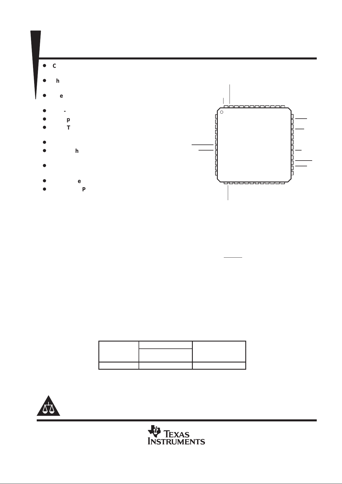
14 15
GND
EN_B
PB
OFF
ON
V
CC
NC
EN
PA
MIC_EN
EN_A
GND
36
35
34
33
32
31
30
29
28
27
26
25
16
1
2
3
4
5
6
7
8
9
10
11
12
GND
V
CC
PL
RNGR_OUT+
RNGR_OUT–
RNGR_IN
RNGR_EN
RESET
NC
AREF
VCP
GND_CP
17 18 19 20
NC
SPKR_OUT+
VB
47 46 45 44 4348 42
ON
SPKR_ENCLVL
NC
REF
VA
CA
GND
NC
MIC_OUT
MIC_IN–
NC
MIC_IN+
40 39 3841
21 22 23 24
37
13
CB
SPKR_IN
SPKR_OUT–
EN_CP
CP
ON_REM
CC
V
PT PACKAGE
(TOP VIEW)
NC – No internal connection
PRODUCTION DATA information is current as of publication date.
Products conform to specifications per the terms of Texas Instruments
standard warranty. Production processing does not necessarily include
testing of all parameters.
Copyright 1998, Texas Instruments Incorporated
TPS9104
CELLULAR SUBSCRIBER TERMINAL
POWER SUPPLY/AUDIO SYSTEM
SLVS133A – AUGUST 1996 – REVISED APRIL 1998
2
POST OFFICE BOX 655303 • DALLAS, TEXAS 75265
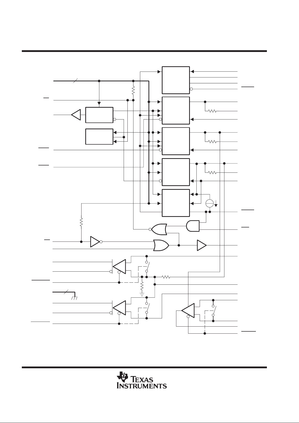
functional block diagram
VA
Charge
Pump
Driver
1 Ω
LDO
Regulator
B
1 Ω
LDO
Regulator
A
1 Ω
LDO
Regulator
L
Reset
Generator
Voltage
Reference
UVLO
†
and
OTP
‡
_
+
_
+
_
+
4
3
VCP
CP
GND_CP
EN_CP
VB
CB
PB
CA
PA
CL
PL
VL
RESET
OFF
ON
SPKR_IN
AREF
RNGR_IN
MIC_IN+
MIC_IN–
MIC_OUT
MIC_EN
V
CC
EN
REF
EN_A
ON
ON_REM
SPKR_OUT+
SPKR_OUT–
SPKR_EN
GND
RNGR_OUT+
RNGR_OUT–
RNGR_EN
EN_B
†
UVLO - Undervoltage lockout
‡
OTP - Overtemperature protection
TPS9104
CELLULAR SUBSCRIBER TERMINAL
POWER SUPPLY/AUDIO SYSTEM
SLVS133A – AUGUST 1996 – REVISED APRIL 1998
3
POST OFFICE BOX 655303 • DALLAS, TEXAS 75265
TPS9104Y chip information
These chips, when properly assembled, display characteristics similar to the TPS9104. Thermal compression
or ultrasonic bonding may be used on the doped aluminum bonding pads. The chips may be mounted with
conductive epoxy or a gold-silicon preform.
CHIP THICKNESS: 15 TYPICAL
BONDING PADS: 3.3 × 3.3 MINIMUM
TJ max = 150°C
TOLERANCES ARE ±10%.
ALL DIMENSIONS ARE IN MILS.
BONDING PAD ASSIGNMENTS
138
138
24
23
22
21
19
18
16
15
14
13
123456784710 11 12
36 35 34 33 32 31 29 28 27 26 25
37
38
39
40
42
43
45
46
48
TPS9104
CELLULAR SUBSCRIBER TERMINAL
POWER SUPPLY/AUDIO SYSTEM
SLVS133A – AUGUST 1996 – REVISED APRIL 1998
4
POST OFFICE BOX 655303 • DALLAS, TEXAS 75265
Terminal Functions
TERMINAL
NAME NO.
I/O
DESCRIPTION
GND 1, 15,
25, 36
Ground. GND terminals should be externally connected to ground to ensure proper functionality.
V
CC
2, 31,
40
Supply voltage input. VCC terminals are not connected internally and must be externally connected to ensure
proper functionality.
PL 3 I Program L. PL provides voltage programming input for regulator L.
RNGR_OUT+ 4 O Ringer amplifier noninverting output
RNGR_OUT– 5 O Ringer amplifier inverting output
RNGR_IN 6 I Ringer amplifier input
RNGR_EN 7 I Ringer amplifier enable input; logic low enables the amplifier
RESET 8 O Microprocessor reset output
NC 9, 17,
20, 30
41, 44
No connection
AREF 10 Analog reference. A 0.1-µF capacitor must be connected from AREF to ground. No other connections are
allowed.
VCP 11 Charge pump driver supply voltage
GND_CP 12 Charge pump driver ground
CP 13 O Charge pump driver output
EN_CP 14 I Charge pump driver enable input. Logic low on EN_CP turns on the charge pump.
ON_REM 16 I Remote on; logic high enables the part.
MIC_OUT 18 O Microphone amplifier output
MIC_IN– 19 I Microphone amplifier inverting input
MIC_IN+ 21 I Microphone amplifier noninverting input
REF 22 O 1.185-V reference output. Decouple with 0.01-µF to 0.1-µF capacitor to ground.
VA 23 O Regulator A output voltage
CA 24 Regulator A filter capacitor connection
EN_A 26 I Regulator A enable input; logic low turns on the regulator.
MIC_EN 27 I Microphone amplifier enable input; logic low turns on the microphone amplifier.
PA 28 I Program A. PA provides programming input for Regulator A.
EN 29 I/O Enable signal input/output; logic low enables the part.
ON 32 O On-signal output
OFF 33 I Off signal
PB 34 I Program B. PB provides programming input for Regulator B.
EN_B 35 I Regulator B enable input; logic low turns on the regulator.
CB 37 Regulator B filter capacitor connection
VB 38 O Regulator B output voltage
SPKR_OUT+ 39 O Speaker amplifier noninverting output
SPKR_OUT– 42 O Speaker amplifier inverting output
SPKR_IN 43 I Speaker amplifier input
VL 45 O Regulator L output voltage
CL 46 Regulator L filter capacitor connection
SPKR_EN 47 I Speaker amplifier enable input; logic low enables the amplifier.
ON 48 I On signal; logic low enables the part.

TPS9104
CELLULAR SUBSCRIBER TERMINAL
POWER SUPPLY/AUDIO SYSTEM
SLVS133A – AUGUST 1996 – REVISED APRIL 1998
5
POST OFFICE BOX 655303 • DALLAS, TEXAS 75265
detailed description
voltage reference
The regulators and reset generator utilize an internal 1.185-V band-gap voltage reference. The reference is also
buffered and brought out on REF for external use; REF can source a maximum of 2 mA. A 0.01-µF to 0.1-µF
capacitor must be connected between REF and ground.
LDO regulators
The TPS 9104 includes three low-dropout regulators, implemented with 1-Ω PMOS series-pass transistors, with
quiescent supply currents of 100 µA. Each of the regulators can supply up to 100 mA of continuous output
current. The 1-Ω PMOS series-pass transistor achieves the dropout voltage of just 100 mV at the maximum
rated output current. Each regulator output voltage can be independently programmed to either 3.3 V or 3 V
using its programming control input PL, P A or PB (Px). A logic low on Px sets the output voltage of the regulator
to 3.3 V; a logic high sets it to 3 V.
Each LDO contains a current limit circuit. When the current demand on the regulator exceeds the current limit,
the output voltage drops in proportion to the excess current. When the excess load current is removed, the
output voltage returns to regulation. Exceeding the current limit on VL can disable the TPS9104. If enough
current demand is placed on VL, the output voltage drops below the reset threshold voltage causing RESET
to go low, effectively unlatching the enable.
VL is intended to be the primary supply voltage for the microprocessor and other system logic functions. V A and
VB can be used to power low-noise analog circuits and/or implement system power management. The enable
terminals EN_A
and EN_B are utilized to power down circuitry when it is not required. EN_A and EN_B are
TTL-compatible inputs with 10-µA active current-source pullups. A logic low enables the respective regulator
while a logic high pulls the regulator output voltage to ground and reduces the regulator quiescent current to
leakage levels. Both EN_A
and EN_B are not active until RESET is logic high.
Stability of the LDOs is ensured by the addition of compensation terminals CL, CA, and CB, which connect to
the output of the regulator through an internal 1-Ω resistor. This compensation scheme allows for capacitors
with equivalent series resistance (ESR) of up to 15 Ω, eliminating the need for expensive, low-ESR capacitors.
reset generator
RESET
is a microprocessor reset signal that goes to logic low at power-up, or whenever VL drops below 2.93 V
(2.6 V for 3-V applications), and remains in that state for 250 ms after VL exceeds the RESET
threshold (see
Figure 5). The open-drain output has a 30-µA pullup that eliminates the need for an external pullup resistor and
still allows it to be connected with other open-drain or open-collector signals. RESET
is valid for supply voltages
as low as 1.5 V.
ON
, OFF, ON, ON_REM and EN functions
The ON
input is intended to be the main enable for the TPS9104 and should be connected to ground through
a push-button switch. Once the switch is pressed, internal logic pulls EN
low. The EN terminal is designed to
sink 3.2 mA and can be used as a pulldown to enable other functions on the TPS9104 or other system circuitry .
When EN
is pulled low, the TPS9104 checks to make sure the supply voltage is above the UVLO threshold
voltage and the die temperature is below 160°C. If both of these conditions are met, the reference circuitry,
regulator L, reset generator, and other support circuitry are enabled. When RESET
goes high, the system can
respond with a logic high on OFF
, which latches the TPS9104 on, and the ON push button can then be released.
The TPS9104 is disabled in a similar manner. If the ON
push button is pressed while the TPS9104 is enabled,
the ON signal responds with a logic high. Once this logic high is detected, the system can respond with a logic
low on OFF
, disabling the TPS9104 and reducing supply currents to 1 µA (see Figure 1).
TPS9104
CELLULAR SUBSCRIBER TERMINAL
POWER SUPPLY/AUDIO SYSTEM
SLVS133A – AUGUST 1996 – REVISED APRIL 1998
6
POST OFFICE BOX 655303 • DALLAS, TEXAS 75265
The ON_REM signal can be used in the same manner as ON in enabling or disabling the TPS9104. The signal
is provided as a system interface to increase the flexibility of the system. EN
can also be used as an input
wired-OR open collector/drain to enable the TPS9104; however, it does not produce a logic signal ON and
therefore cannot be used in the disable sequence described above. It is not recommended that EN
be used as
the primary enable signal for the TPS9104.
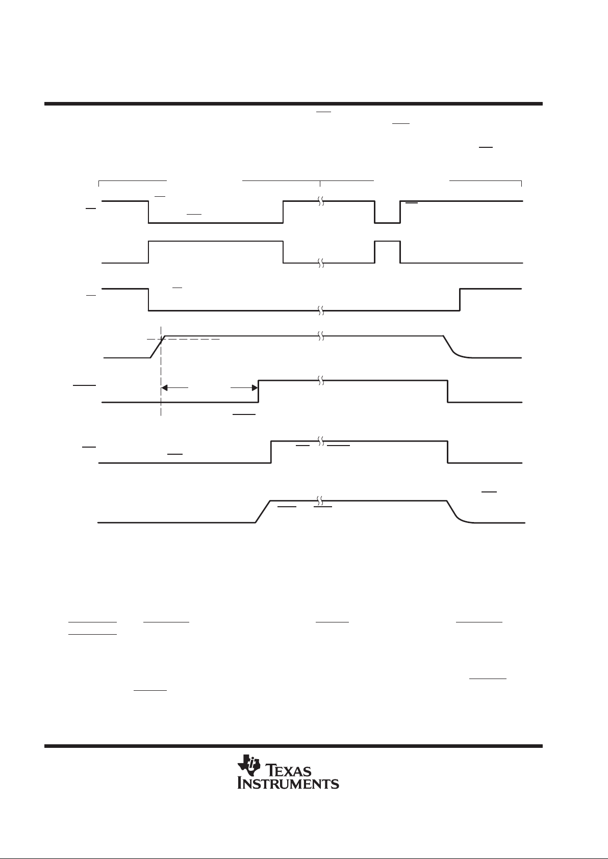
Enable Sequence Disable Sequence
ON
Must Be Held Low Until
System Responds With A High
Signal At OFF .
ON Is Pressed To Turn Off
The System (Phone).
Once EN
Goes Low, The Status Of The
UVLO And The OTP Are Checked.
If The UVLO And OTP Are Valid, VL
And Other Functions Are Enabled.
250 ms
250 ms After VL Rises Above The Reset
Threshold Voltage, RESET Goes High.
The System Can Now
Respond With A High Signal
At OFF.
Once OFF And RESET Are High,
The Enable Input Is Latched On.
System Detects The High
Signal At ON And
Responds With a Low
Signal At OFF .
ON
ONENON
VL
RESET
OFF
VA
VB
EN_A And EN_B Are both Active And
Low.
Figure 1. Recommended Enable and Disable Sequence
speaker/ringer power amplifiers
The TPS9104 includes two differential-output power amplifiers capable of driving dynamic or piezoelectric
speakers. Both amplifiers have enable inputs to reduce supply current to leakage levels when the amplifiers
are not in use. Depopping circuitry prevents objectionable noise when the enable inputs are cycled on or off.
Each amplifier requires only two gain-setting resistors and a capacitor for dc blocking (see Figure 46).
RNGR_EN
and SPKR_EN inputs are disabled when RESET is asserted. Both the SPKR_EN and the
RNGR_EN
have internal 10-µA pullups.
microphone amplifier
This is a high-gain amplifier capable of driving a 10-kΩ load at 3 V peak-to-peak output. MIC_EN
input is
disabled when RESET
is asserted. The microphone amplifier has an enable input that reduces supply current
to leakage levels when disabled. Added depopping circuitry prevents objectionable noise when the enable input
TPS9104
CELLULAR SUBSCRIBER TERMINAL
POWER SUPPLY/AUDIO SYSTEM
SLVS133A – AUGUST 1996 – REVISED APRIL 1998
7
POST OFFICE BOX 655303 • DALLAS, TEXAS 75265
is cycled on or off. The microphone amplifier needs only two resistors to set the gain, and one capacitor for dc
blocking (see Figure 47). Regulator A is the analog supply for the microphone amplifier, and EN_A
must be
asserted for correct operation.
undervoltage lockout
Undervoltage lockout (UVLO) prevents operation of the functions in the TPS9104 until the supply voltage
exceeds the threshold voltage, eliminating abnormal power-up conditions internally and externally, and
providing an orderly turn-on.
overtemperature shutdown
If the die temperature exceeds 160°C, the thermal protection circuit shuts off the TPS9104. When the die
temperature drops below 150°C, the device can be restarted with the ON
input.
charge pump driver
An unregulated inverting or doubler charge pump is implemented (see Figure 44) by connecting a network of
two capacitors and two diodes to CP. In the inverting configuration, the charge pump can power an LCD or
provide gate bias for a GaAs power amplifier. A 5-V supply for flash-memory programming or powering the
subscriber identity module (SIM) European applications can be achieved using the doubler configuration and
an external LDO. A logic-low input to the charge-pump enable, EN_CP
, turns on the oscillator and driver; a logic
high turns them off. EN_CP
input is disabled when RESET is asserted. The EN_CP has a 10-µA internal pullup.
DISSIPATION RATING TABLE 1 – Free-Air Temperature
PACKAGE
TA ≤ 25°C
POWER RATING
DERATING FACTOR
ABOVE TA = 25°C
TA = 70°C
POWER RATING
TA = 85°C
POWER RATING
PT 1350 mW 10.8 mW/°C 864 mW 702 mW
DISSIPATION RATING TABLE 2 – Case T emperature
PACKAGE
TC ≤ 25°C
POWER RATING
DERATING FACTOR
ABOVE TC = 25°C
TC = 70°C
POWER RATING
TC= 85°C
POWER RATING
PT 6579 mW 52.6 mW/°C 4212 mW 3423 mW
TPS9104
CELLULAR SUBSCRIBER TERMINAL
POWER SUPPLY/AUDIO SYSTEM
SLVS133A – AUGUST 1996 – REVISED APRIL 1998
8
POST OFFICE BOX 655303 • DALLAS, TEXAS 75265
400
200
1200
0
25 50 75 100
800
600
1000
MAXIMUM CONTINUOUS POWER DISSIPATION
vs
FREE-AIR TEMPERATURE
1400
125 150
TA – Free-Air Temperature – °C
R
θJA
= 93°C/W
– Maximum Continuous Power Dissipation – mW
P
D
2000
1000
6000
0
25 50 75 100
– Maximum Continuous Power Dissipation – mW
4000
3000
5000
MAXIMUM CONTINUOUS POWER DISSIPATION
vs
CASE TEMPERATURE
7000
125 150
TA – Case Temperature – ° C
R
θJC
= 19°C/W
P
D
Figure 2 Figure 3
absolute maximum ratings over operating free-air temperature range (unless otherwise noted)
†‡
Supply voltage range, V
CC
, VCP –0.3 V to 12 V. . . . . . . . . . . . . . . . . . . . . . . . . . . . . . . . . . . . . . . . . . . . . . . . . . . .
Input voltage range at OFF
, MIC_EN, SPKR_EN, RNGR_EN, SPKR_IN,
RNGR_IN, MIC_IN+, MIC_IN– –0.3 V to 7 V. . . . . . . . . . . . . . . . . . . . . . . . . . . . . . . . . . . . . . . . . . . . . . . . . .
Input voltage range at PL, PA, PB, EN
, EN_A, EN_B,
ON
, ON_REM, EN_CP –0.3 V to V
CC
. . . . . . . . . . . . . . . . . . . . . . . . . . . . . . . . . . . . . . . . . . . . . . . . . . . . . . .
Continuous total power dissipation See dissipation rating table. . . . . . . . . . . . . . . . . . . . . . . . . . . . . . . . . . . . . . .
Peak output current Internally limited. . . . . . . . . . . . . . . . . . . . . . . . . . . . . . . . . . . . . . . . . . . . . . . . . . . . . . . . . . . . . .
Output current range at SPKR_OUT+, SPKR_OUT–,
RNGR_OUT+, RNGR_OUT– –100 mA to 100 mA. . . . . . . . . . . . . . . . . . . . . . . . . . . . . . . . . . . . . . . . . . . . .
Power dissipation See dissipation rating table. . . . . . . . . . . . . . . . . . . . . . . . . . . . . . . . . . . . . . . . . . . . . . . . . . . . . .
Operating free-air temperature range, T
A
–40°C to 85°C. . . . . . . . . . . . . . . . . . . . . . . . . . . . . . . . . . . . . . . . . . . .
Storage temperature range, T
stg
–65°C to 150°C. . . . . . . . . . . . . . . . . . . . . . . . . . . . . . . . . . . . . . . . . . . . . . . . . . .
Lead Temperature 1,6 mm (1/16 inch) from case for 10 seconds 260°C. . . . . . . . . . . . . . . . . . . . . . . . . . . . . . .
†
Stresses beyond those listed under “absolute maximum ratings” may cause permanent damage to the device. These are stress ratings only, and
functional operation of the device at these or any other conditions beyond those indicated under “recommended operating conditions” is not
implied. Exposure to absolute-maximum-rated conditions for extended periods may affect device reliability.
‡
All voltages are with respect to GND.
TPS9104
CELLULAR SUBSCRIBER TERMINAL
POWER SUPPLY/AUDIO SYSTEM
SLVS133A – AUGUST 1996 – REVISED APRIL 1998
9
POST OFFICE BOX 655303 • DALLAS, TEXAS 75265
recommended operating conditions
MIN NOM MAX UNIT
Supply voltage, VCC, VCP 3 10 V
Input voltage, OFF, MIC_EN, SPKR_EN, RNGR_EN 0 5 V
Input voltage at PL, PA, PB, EN, EN_A, EN_B, ON, ON_REM, EN_CP 0 V
CC
V
Reference output current 0 2 mA
Continuous regulator output current 0 100 mA
Operating free-air temperature –40 85 °C
electrical characteristics over recommended operating free-air temperature range,
V
CC
= VCP = 4 V, Px = 0 V, I
O(Vx)
= 35 mA, OFF = VL, ON open, ON_REM = 0 V, Cx = 10 µF
(unless otherwise noted)
voltage reference (REF)
PARAMETER TEST CONDITIONS
†
MIN TYP MAX UNIT
p
TA = 25°C, IO = 0 1.185 V
Output voltage
4 V ≤ VCC ≤ 10 V, 0 ≤ IO≤ 2 mA 1.161 1.209 V
LDO regulators
PARAMETER TEST CONDITIONS
†
MIN TYP MAX UNIT
TA = 25°C 3.25 3.3 3.35 V
0 ≤ I
O(Vx)
≤ 100 mA, 3.5 V ≤ VCC ≤ 10 V 3.2 3.4 V
Output voltage at VA, VB, VL (Vx)
Px = VCC,
TA = 25°C 2.95 3 3.05 V
Px = V
CC,
3.2 V ≤ VCC ≤ 10 V
0 ≤ I
O(Vx)
≤ 100 mA,
2.9 3.10 V
Dropout voltage I
O(Vx)
= 100 mA, VCC = 3.2 V 100 200 mV
Load regulation I
O(Vx)
= 0 mA to 100 mA 30 mV
Line regulation I
O(Vx)
= 100 mA, VCC = 3.5 V to 10 V 10 mV
Ripple rejection f = 120 Hz 60 dB
Quiescent current (each regulator) 100 µA
charge pump driver
PARAMETER TEST CONDITIONS MIN TYP MAX UNIT
Frequency 50 100 150 kHz
Duty cycle 50%
Output resistance 15 30 Ω
†
Pulse-testing techniques are used to maintain virtual junction temperature as close as possible to ambient temperature; thermal effect must be
taken into account separately.
TPS9104
CELLULAR SUBSCRIBER TERMINAL
POWER SUPPLY/AUDIO SYSTEM
SLVS133A – AUGUST 1996 – REVISED APRIL 1998
10
POST OFFICE BOX 655303 • DALLAS, TEXAS 75265
electrical characteristics over recommended operating free-air temperature range,
V
CC
= VCP = 4 V, Px = 0 V, I
O(Vx)
= 35 mA, OFF = VL, ON open, ON_REM = 0 V, Cx = 10 µF
(unless otherwise noted) (continued)
speaker amplifier/ringer amplifier
PARAMETER TEST CONDITIONS
†
MIN TYP MAX UNIT
Output voltage swing Single-ended, RL = 32 Ω 1.6 2 V
Output offset voltage Av = 1 V/V 15 30 mV
Total harmonic distortion (THD)
V
I(PP)
= 1 V,
Av = 1 V/V,
f = 1 kHz,
RL = 32 Ω
0.5% 1%
Gain bandwidth product (GBW) Av = 10 V/V 4 20 kHz
Input noise 100 Hz ≤ BW ≤ 100 kHz 200 µVrms
Quiescent current (each amplifier) 2 mA
PL = V
CC
1.221
Reference voltage, AREF
PL = 0 V 1.345
V
microphone amplifier
PARAMETER TEST CONDITIONS
†
MIN TYP MAX UNIT
Common mode input voltage range 1 VA –1 V
Input bias current Both inputs = VA/2 –1 1 µA
Output voltage swing 10 kΩ load, VA = 3.3 V 2.7 3 V
Output offset voltage Av = 1 V/V 6 mV
Total harmonic distortion (THD)
f = 1 kHz, AV = 100 V/V ,
Output voltage swing = 1 V , V
O(PP)
0.5% 1%
Power-supply rejection ratio (PSRR) Av = 100 V/V 100 dB
Common-mode rejection ratio (CMRR) Av = 100 V/V 80 dB
Gain bandwidth product (GBW) Av = 100 V/V 4 kHz
Input noise 100 Hz ≤ BW ≤ 100 kHz 10 µVrms
Quiescent current 180 µA
RESET
PARAMETER TEST CONDITIONS
†
MIN TYP MAX UNIT
Input threshold voltage VL voltage decreasing 2.871 2.93 2.989 V
Input threshold voltage VL voltage decreasing, PL = V
CC
2.548 2.6 2.652 V
Timeout delay at RESET See Figure 5 125 250 375 ms
Low-level output voltage IO = 1 mA, VCC = 1.5 V 0.4 V
High-level output current VO = 2.4 V –40 –20 µA
Low-level output current VO = 0.4 V 3.2 mA
Hysteresis 40 mV
logic inputs at EN_A, EN_B, SPKR_EN, RNGR_EN, MIC_EN, EN_CP
PARAMETER TEST CONDITIONS MIN TYP MAX UNIT
High-level input voltage 2 V
Low-level input voltage 0.8 V
Input current –20 –10 1 µA
†
Pulse-testing techniques are used to maintain virtual junction temperature as close as possible to ambient temperature; thermal effect must be
taken into account separately.

TPS9104
CELLULAR SUBSCRIBER TERMINAL
POWER SUPPLY/AUDIO SYSTEM
SLVS133A – AUGUST 1996 – REVISED APRIL 1998
11
POST OFFICE BOX 655303 • DALLAS, TEXAS 75265
electrical characteristics over recommended operating free-air temperature range,
V
CC
= VCP = 4 V, Px = 0 V, I
O(Vx)
= 35 mA, OFF = VL, ON open, ON_REM = 0 V, Cx = 10 µF
(unless otherwise noted) (continued)
logic inputs at PL, PA, PB, OFF, ON_REM
PARAMETER TEST CONDITIONS MIN TYP MAX UNIT
High-level input voltage 2 V
Low-level input voltage 0.8 V
Input current –1 1 µA
logic inputs at ON
†
PARAMETER TEST CONDITIONS MIN TYP MAX UNIT
High-level input voltage 2 V
Low-level input voltage 0.8 V
Input current –20 1 µA
logic inputs at EN
†
PARAMETER TEST CONDITIONS MIN TYP MAX UNIT
High-level input voltage 2.4 V
Low-level input voltage 0.8 V
Source current VO = 2.4 V OFF = 0 –50 –30 1 µA
Sink current VO = 0.4 V 3.2 mA
logic outputs at ON
PARAMETER TEST CONDITIONS MIN TYP MAX UNIT
High-level output voltage 1-mA source current 2.4 V
Low-level output voltage 1-mA sink current 0.4 V
overtemperature shutdown
PARAMETER TEST CONDITIONS MIN TYP MAX UNIT
T emperature threshold 160 °C
Temperature hysteresis 10 °C
undervoltage lockout (UVLO)
PARAMETER TEST CONDITIONS MIN TYP MAX UNIT
Threshold VCC increasing 1.80 2.52 V
Hysteresis 50 mV
supply current
PARAMETER TEST CONDITIONS MIN TYP MAX UNIT
Shutdown OFF = 0 V 0.5 10 µA
Operating
EN_CP = VCP,
RNGR_EN
= VL,
SPKR_EN = VL,
MIC_EN
= VL
0.7 1 mA
†
High and low level voltages are dependent on VCC. See graphs.

TPS9104
CELLULAR SUBSCRIBER TERMINAL
POWER SUPPLY/AUDIO SYSTEM
SLVS133A – AUGUST 1996 – REVISED APRIL 1998
12
POST OFFICE BOX 655303 • DALLAS, TEXAS 75265
TPS9104Y electrical characteristics, T
J
= 25°C, V
CC
= VCP = 4 V, Px = 0 V, I
O(Vx)
= 35 mA,
OFF
= VL, ON open, ON_REM = 0 V, Cx
=
10 µF (unless otherwise noted)
voltage reference (REF)
PARAMETER
TEST CONDITIONS
†
MIN TYP MAX UNIT
Output voltage IO = 0 1.185 V
LDO Regulators
PARAMETER TEST CONDITIONS
†
MIN TYP MAX UNIT
Output voltage at VA, VB, VL (Vx) Px = V
CC
2.95 3 3.05 V
Dropout voltage I
O(Vx)
= 100 mA, VCC = 3.2 V 100 mV
Load regulation I
O(Vx)
= 0 mA to 100 mA 30 mV
Line regulation I
O(Vx)
= 100 mA, VCC = 3.5 V to 10 V 10 mV
Ripple rejection f = 120 Hz 60 dB
Quiescent current (each regulator) 100 µA
charge pump driver
PARAMETER TEST CONDITIONS MIN TYP MAX UNIT
Frequency 100 kHz
Duty cycle 50%
Output resistance 15 Ω
speaker amplifier/ringer amplifier
PARAMETER TEST CONDITIONS
†
MIN TYP MAX UNIT
Output voltage swing Single-ended, RL = 32 Ω 2 V
Output offset voltage Av = 1 V/V 15 mV
Total harmonic distortion (THD)
V
I(PP)
= 1 V,
Av = 1 V/V,
f = 1 kHz,
RL = 32 Ω
0.5%
Gain bandwidth product (GBW) Av = 10 V/V 20 kHz
Input noise 100 Hz ≤ BW ≤ 100 kHz 200 µVrms
Quiescent current (each amplifier) 2 mA
PL = V
CC
1.221
Reference, AREF
PL = 0 V 1.345
V
microphone amplifier
PARAMETER TEST CONDITIONS
†
MIN TYP MAX UNIT
Common mode input range 1 VA –1 V
Output voltage swing 10 kΩ load, VA = 3.3 V 2.7 3 V
Output offset voltage Av = 1 V/V 6 mV
RESET
PARAMETER TEST CONDITIONS
†
MIN TYP MAX UNIT
Threshold voltage VL voltage decreasing 2.93 V
Threshold voltage VL voltage decreasing, PL = V
CC
2.6 V
Delay See Figure 5 250 ms
Hysteresis 40 mV
†
Pulse-testing techniques are used to maintain virtual junction temperature as close as possible to ambient temperature; thermal effect must be
taken into account separately.

TPS9104
CELLULAR SUBSCRIBER TERMINAL
POWER SUPPLY/AUDIO SYSTEM
SLVS133A – AUGUST 1996 – REVISED APRIL 1998
13
POST OFFICE BOX 655303 • DALLAS, TEXAS 75265
PARAMETER MEASUREMENT INFORMATION
_
+
Charge Pump
Driver
Regulator
B
Regulator
A
Reset
Generator
_
+
_
+
RESET
OFF
ON
Voltage
Reference
REF
REF
ON
ON_REM
VL
V
I(test)
EN
LOAD
Regulator
L
LOAD
10 µF
10 µF
10 µF
VL
V
CC
40 2 31 11
13
12
38
37
34
23
24
28
45
46
3
8
33
32
42
39
47
4
5
7
18
27
22
14
35
26
29
48
16
43
10
6
21
19
36 1 25 15
0.1 µF
0.1 µF
0.1 µF
+
+
+
LOAD
Figure 4. Test Circuit

TPS9104
CELLULAR SUBSCRIBER TERMINAL
POWER SUPPLY/AUDIO SYSTEM
SLVS133A – AUGUST 1996 – REVISED APRIL 1998
14
POST OFFICE BOX 655303 • DALLAS, TEXAS 75265
PARAMETER MEASUREMENT INFORMATION
t
t
RESET
Timeout Delay
RESET
V
IT+
VL
Figure 5. RESET Timing Diagram
04 812
Enable Input Voltage – V
3
4
t – Time – ms
5
16 20
2
1
0
4
3
2
1
0
– Output Voltage – V
V
O
Enable
V
O
VCC = 4 V
Px = 0 V
TA = 25°C
IO = 0 mA
Cx = 10 µF
Figure 6. LDO Regulator Output Voltage Rise Time and Fall Time

TPS9104
CELLULAR SUBSCRIBER TERMINAL
POWER SUPPLY/AUDIO SYSTEM
SLVS133A – AUGUST 1996 – REVISED APRIL 1998
15
POST OFFICE BOX 655303 • DALLAS, TEXAS 75265
PARAMETER MEASUREMENT INFORMATION
0 0.5 1
– LDO Regulator
25
75
t – Time – ms
125
1.5 2
100
50
0
3.5
3.4
3.3
3.2
3.1
I
O
– Output Voltage – V
V
O
VCC = 4 V
Px = 0 V
TA = 25°C
Cx = 10 µF
Output Current – mA
Figure 7. LDO Regulator Load Transient, 1 mA to 100 mA Pulsed Load
0 0.3 0.5
– Supply Voltage – V
3.6
4
t – Time – ms
4.4
0.8 1
4.2
3.8
3.4
3.3
3.2
3.1
V
CC
Px = 0 V
TA = 25°C
IO = 10 mA
Cx = 10 µF
– Output Voltage – V
V
O
Figure 8. LDO Regulator Line Transient

TPS9104
CELLULAR SUBSCRIBER TERMINAL
POWER SUPPLY/AUDIO SYSTEM
SLVS133A – AUGUST 1996 – REVISED APRIL 1998
16
POST OFFICE BOX 655303 • DALLAS, TEXAS 75265
PARAMETER MEASUREMENT INFORMATION
0102030
– Input Voltage, MIC_EN – V
1
3
5
40 50
4
2
3.5
3
2.5
2
1.5
1
0.5
– Output Voltage, MIC_OUT – V
V
I
V
O
t – Time – µs
VCC = 4 V
TA = 25°C
Px = 0 V
Figure 9. Microphone Enable Output Response
0
0102030
– Input Voltage, SPKR_EN – V
1
4
5
40 50
3
2
2.5
2
1.5
1
0.5
– Output Voltage, SPKR_OUT+ – V
V
I
V
O
t – Time – µs
VCC = 4 V
TA = 25°C
Px = 0 V
Figure 10. Speaker Enable Output Response

TPS9104
CELLULAR SUBSCRIBER TERMINAL
POWER SUPPLY/AUDIO SYSTEM
SLVS133A – AUGUST 1996 – REVISED APRIL 1998
17
POST OFFICE BOX 655303 • DALLAS, TEXAS 75265
PARAMETER MEASUREMENT INFORMATION
0102030
– Input Voltage, RNGR_EN –
V
1
3
5
40 50
4
2
0
3
2.5
2
1.5
1
0.5
V
I
– Output Voltage, RNGR_OUT+ – V
V
O
t – Time – µs
VCC = 4 V
TA = 25°C
Px = 0 V
Figure 11. Ringer Enable Output Response
2
1
0
0102030
3
4
40 50
– Output Voltage, MIC_OUT – V
t – Time – µs
V
O
Figure 12. Microphone Slew Rate, Rising Figure 13. Microphone Slew Rate, Falling
1
0
0 102030
– Output Voltage, MIC_OUT – V
2
3
40 50
t – Time – µs
V
O
4
VCC = 4 V
TA = 25°C
Px = 0 V
VCC = 4 V
TA = 25°C
Px = 0 V

TPS9104
CELLULAR SUBSCRIBER TERMINAL
POWER SUPPLY/AUDIO SYSTEM
SLVS133A – AUGUST 1996 – REVISED APRIL 1998
18
POST OFFICE BOX 655303 • DALLAS, TEXAS 75265
TYPICAL CHARACTERISTICS
Table of Graphs
FIGURE
I
CC
Quiescent current vs Supply voltage 14
p
vs Output current 15
Dropout voltage
vs Junction temperature 16
∆V
O
Change in output voltage vs Junction temperature 17
V
O
Output voltage, VL vs Supply voltage 18
∆V
O
Change in output voltage vs Supply voltage 19
∆V
O
Change in output voltage vs Output current 20
I
CC
Shutdown current vs Supply voltage 21
Threshold, ON vs Supply voltage 22
Threshold, EN vs Supply voltage 23
Threshold, ON_REM vs Supply voltage 24
Ripple rejection vs Frequency 25
Output spectral noise density vs Frequency 26
Change in frequency, CP vs Junction temperature 27
r
O
Output resistance into CP vs Supply voltage 28
r
O
Output resistance out of CP vs Supply voltage 29
V
OM
Maximum peak output voltage vs Load resistance 30
vs Frequency 31
THD
Total harmonic distortion
vs Load resistance 32
k
SVR
Power supply rejection ratio vs Frequency 33
V
n
Output noise voltage vs Frequency 34
V
O
Output voltage vs Junction temperature 35
V
OM
Maximum peak output voltage vs Load 36
vs Frequency 37
THD
Total harmonic distortion
vs Load resistance 38
k
SVR
Power supply rejection ratio vs Frequency 39
Closed-loop gain and phase shift vs Frequency 40
V
n
Output noise voltage vs Frequency 41
Φ
m
Phase margin vs Load capacitance 42

TPS9104
CELLULAR SUBSCRIBER TERMINAL
POWER SUPPLY/AUDIO SYSTEM
SLVS133A – AUGUST 1996 – REVISED APRIL 1998
19
POST OFFICE BOX 655303 • DALLAS, TEXAS 75265
TYPICAL CHARACTERISTICS
Figure 14
–40°C
85°C
25°C
0.7
0.6
0.5
345 6
– Quiesent Current – mA
0.8
0.9
QUIESENT CURRENT
vs
SUPPLY VOLTAGE
1
79108
I
CC
VCC – Supply Voltage – V
Px = 0
IO = 0
Figure 15
Dropout Voltage – mV
IO – Output Current – mA
DROPOUT VOLTAGE
vs
OUTPUT CURRENT
80
60
20
0
0102030405060
100
140
160
70 80 90 100
40
120
Px = V
CC
Px = 0
TA = 25°C
LDO REGULATORS
Figure 16
100
80
70
60
Dropout Voltage – mV
120
130
DROPOUT VOLTAGE
vs
JUNCTION TEMPERATURE
140
110
90
–50 –25 0 25 50 75 100 125
TJ – Temperature – ° C
IO = 100 mA
Px = 0
LDO REGULATORS
Figure 17
0
–4
–6
–10
–50 –25 0 25 50
– Change in Output Voltage – mV
4
6
10
75 100 125
8
2
–2
–8
CHANGE IN OUTPUT VOLTAGE
vs
JUNCTION TEMPERATURE
LDO REGULATORS
VCC = 4 V
Px = 0
IO = 0 mA
IO = 100 mA
∆V
O
TJ – Temperature – ° C

TPS9104
CELLULAR SUBSCRIBER TERMINAL
POWER SUPPLY/AUDIO SYSTEM
SLVS133A – AUGUST 1996 – REVISED APRIL 1998
20
POST OFFICE BOX 655303 • DALLAS, TEXAS 75265
TYPICAL CHARACTERISTICS
Figure 18
1
0.5
3
0
2 2.2 2.4 2.6 2.8 3 3.2
– Output Voltage, VL – V
2
1.5
2.5
OUTPUT VOLTAGE
vs
SUPPLY VOLTAGE
3.5
3.4 3.6 3.8 4
Px = 0
TA = 25°C
EN
= 0
V
O
VCC – Supply Voltage – V
REGULATOR L
Figure 19
0
–1
–3
–4
345 6 7
1
3
CHANGE IN OUTPUT VOLTAGE
vs
SUPPLY VOLTAGE
4
8910
2
–2
VCC – Supply Voltage – V
Px = 0 or
Px = V
CC
TA = 25°C
IO = 35 mA
LDO REGULATORS
– Change in Output Voltage – mV
∆V
O
Figure 20
CHANGE IN OUTPUT VOLTAGE
vs
OUTPUT CURRENT
0
–5
–15
–20
0102030405060
5
15
20
70 80 90 100
10
–10
IO – Output Current – mA
VCC = 4 V
Px = 0 or Px = V
CC
TA = 25°C
LDO REGULATORS
– Change in Output Voltage – mV
∆V
O
Figure 21
2
1.5
0.5
0
23 4 5 6 7
– Shutdown Current –
2.5
3.5
SHUTDOWN CURRENT
vs
SUPPLY VOLTAGE
4
8910
3
1
OFF = 0
TA = 40°C
TA = 25°C
TA = 85°C
AµI
CC
VCC – Supply Voltage – V

TPS9104
CELLULAR SUBSCRIBER TERMINAL
POWER SUPPLY/AUDIO SYSTEM
SLVS133A – AUGUST 1996 – REVISED APRIL 1998
21
POST OFFICE BOX 655303 • DALLAS, TEXAS 75265
TYPICAL CHARACTERISTICS
Figure 22
1.2
1
0.8
246
– Input Threshold Voltage, ON – V
1.4
1.6
INPUT THRESHOLD VOLTAGE, ON
vs
SUPPLY VOLTAGE
1.8
810
V
CC
– Supply Voltage – V
–40°C
25°C
85°C
OFF = 0 V
EN
= Open
ON_REM = 0 V
V
IT
Figure 23
VCC – Supply Voltage – V
2.4
1.9
4.4
1.4
2345 67
3.4
2.9
3.9
INPUT THRESHOLD VOLTAGE, EN
vs
SUPPLY VOLTAGE
4.9
8910
OFF = 0 V
ON
= Open
ON_REM = 0 V
– Input Threshold Voltage, EN – VV
IT
Figure 24
2.5
2
1.5
1
234
3
3.5
INPUT THRESHOLD VOLTAGE, ON_REM
vs
SUPPLY VOLTAGE
4
56 8
97
VCC – Supply Voltage – V
EN = Open
ON
= Open
OFF
= 0 V
10
– Input Threshold Voltage, ON_REM – VV
IT
Figure 25
60
40
20
80
0.01 0.1 1 10 100 1000
Ripple Rejection – dB
f – Frequency – kHz
RIPPLE REJECTION
vs
FREQUENCY
LDO REGULATORS
VCC = 4 V
TA = 25°C
Cx = 10 µF
IO = 35 mA

TPS9104
CELLULAR SUBSCRIBER TERMINAL
POWER SUPPLY/AUDIO SYSTEM
SLVS133A – AUGUST 1996 – REVISED APRIL 1998
22
POST OFFICE BOX 655303 • DALLAS, TEXAS 75265
TYPICAL CHARACTERISTICS
Figure 26
10
1
100
1 10 100 1000 10000
Output Spectral Noise Density –
f – Frequency – Hz
OUTPUT SPECTRAL NOISE DENSITY
vs
FREQUENCY
REGULATOR L
Hz
V / µ
VCC = 4 V
Px = 0 V
TA = 25°C
IO = 35 mA
Figure 27
–1
–2
3
–3
–50 –25 0 25 50
– Change in Frequency, CP – kHz
1
0
2
CHANGE IN FREQUENCY, CP
vs
JUNCTION TEMPERATURE
4
75 100 125
TJ – Temperature – ° C
∆f
VCP = 4 V
Figure 28
34 5 6 7
– Output Resistance, CP –
OUTPUT RESISTANCE, CP
vs
SUPPLY VOLTAGE
8910
V
CC(VCP)
– Supply Voltage – V
r
o
Ω
85°C
25°C
–40°C
Current Into CP
30
25
20
15
10
5
0
Figure 29
15
10
5
0
34 5 6 7
20
25
OUTPUT RESISTANCE, CP
vs
SUPPLY VOLTAGE
30
8910
– Output Resistance, CP –
V
CC(VCP)
– Supply Voltage – V
r
o
Ω
25°C
85°C
–40°C
Current Out of CP

TPS9104
CELLULAR SUBSCRIBER TERMINAL
POWER SUPPLY/AUDIO SYSTEM
SLVS133A – AUGUST 1996 – REVISED APRIL 1998
23
POST OFFICE BOX 655303 • DALLAS, TEXAS 75265
TYPICAL CHARACTERISTICS
Figure 30
2
1.6
1.2
1
10 100
– Maximum Peak Output Voltage – V
2.2
2.6
MAXIMUM PEAK OUTPUT VOLTAGE
vs
LOAD RESISTANCE
3
1000
2.8
2.4
1.8
1.4
Px = 0 V
VCC = 4 V
TA = 25°C
f = 1 kHz
Av = 1 V/V
SPEAKER AND RINGER AMPLIFIERS
V
OM
RL – Load Resistance – Ω
Figure 31
1
0
0.1 1
THD – Total Harmonic Distortion – %
2
f – Frequency – kHz
TOTAL HARMONIC DISTORTION
vs
FREQUENCY
3
10
SPEAKER AND RINGER AMPLIFIERS
Px = 0 V
VCC = 4 V
TA = 25°C
V
O(PP)
= 1 V
RL = 32 Ω
Av = 1 V/V
Figure 32
0.3
0.2
0.1
0
0 500 1000 1500
THD – Total Harmonic Distortion – %
0.4
0.5
TOTAL HARMONIC DISTORTION
vs
LOAD RESISTANCE
0.6
2000 2500 3000
SPEAKER AND RINGER AMPLIFIERS
RL – Load Resistance – Ω
Px = 0 V
VCC = 4 V
TA = 25°C
f = 1 kHz
V
O(PP)
= 1 V
Av = 1 V/V
Figure 33
40
20
0
0.01 0.1 1 10
– Power Supply Rejection Ratio – dB
60
80
f – Frequency – kHz
POWER SUPPLY REJECTION RATIO
vs
FREQUENCY
100
100 1000
SPEAKER AND RINGER AMPLIFIERS
k
SVR
Px = 0 V
VCC = 4 V
TA = 25°C
TPS9104
CELLULAR SUBSCRIBER TERMINAL
POWER SUPPLY/AUDIO SYSTEM
SLVS133A – AUGUST 1996 – REVISED APRIL 1998
24
POST OFFICE BOX 655303 • DALLAS, TEXAS 75265
TYPICAL CHARACTERISTICS
Figure 34
100
50
0
0.1 1
– Output Noise Voltage – nV
150
f – Frequency – kHz
OUTPUT NOISE VOLTAGE
vs
FREQUENCY
200
10
SPEAKER AND RINGER AMPLIFIERS
V
n
Px = 0 V
VCC = 4 V
TA = 25°C
Figure 35
1.9
1.8
1.7
1.6
– Output Voltage – V
2
2.1
OUTPUT VOLTAGE
vs
JUNCTION TEMPERATURE
2.2
SPEAKER AND RINGER AMPLIFIERS
–55 –25 0 25 50 75 100 125
TJ – Temperature – ° C
V
O
Px = 0 V
VCC = 4 V
Figure 36
3
2
1.5
1
3.5
2.5
100 1 k 10 k 100 k
– Maximum Peak Output Voltage – V
MAXIMUM PEAK OUTPUT VOLTAGE
vs
LOAD RESISTANCE
MICROPHONE AMPLIFIER
RL – Load Resistance – Ω
V
OM
VCC = 4 V
Px = 0 V
TA = 25°C
f = 1 kHz
Av = 100 V/V
Figure 37
0.18
0.16
0.14
0.12
0.1 1
THD – Total Harmonic Distortion – %
0.2
0.22
f – Frequency – kHz
TOTAL HARMONIC DISTORTION
vs
FREQUENCY
0.24
10
MICROPHONE AMPLIFIER
VCC = 4 V
Px = 0 V
TA = 25°C

TPS9104
CELLULAR SUBSCRIBER TERMINAL
POWER SUPPLY/AUDIO SYSTEM
SLVS133A – AUGUST 1996 – REVISED APRIL 1998
25
POST OFFICE BOX 655303 • DALLAS, TEXAS 75265
TYPICAL CHARACTERISTICS
Figure 38
0.2
0.15
0.1
0102030
THD – Total Harmonic Distortion – %
0.25
0.3
TOTAL HARMONIC DISTORTION
vs
LOAD RESISTANCE
0.35
40 50 60
RL – Load Resistance – kΩ
MICROPHONE AMPLIFIER
VCC = 4 V
Px = 0 V
TA = 25°C
Figure 39
60
40
20
0.01 0.1 1 10
– Power Supply Rejection Ratio – dB
80
f– Frequency – kHz
POWER SUPPLY REJECTION RATIO
vs
FREQUENCY
100
100 1000
MICROPHONE AMPLIFIER
k
SVR
VCC = 4 V
Px = 0 V
TA = 25°C
Figure 40
Figure 41
Gain
Phase
10
0
–10
110
Closed-Loop Gain – dB
20
30
f – Frequency – kHz
CLOSED-LOOP GAIN AND PHASE SHIFT
vs
FREQUENCY
40
100 1000
MICROPHONE AMPLIFIER
225°
180°
135°
90°
45°
0°
Phase Shift
VCC = 4 V
Px = 0 V
Av = 100
RL = 10 kΩ
TA = 25°C
40
20
0
1 10 100
– Output Noise Voltage – nV
60
80
f – Frequency – Hz
OUTPUT NOISE VOLTAGE
vs
FREQUENCY
100
1000 10000
MICROPHONE AMPLIFIER
V
n
VCC = 4 V
Px = 0 V
TA = 25°C

TPS9104
CELLULAR SUBSCRIBER TERMINAL
POWER SUPPLY/AUDIO SYSTEM
SLVS133A – AUGUST 1996 – REVISED APRIL 1998
26
POST OFFICE BOX 655303 • DALLAS, TEXAS 75265
TYPICAL CHARACTERISTICS
0 0.2 0.4 0.6
– Phase Margin
PHASE MARGIN
vs
LOAD CAPACITANCE
0.8 1
80°
60°
40°
20°
0°
MICROPHONE AMPLIFIER
m
φ
CL – Load Capacitance – µF
Figure 42
VCC = 4 V
Px = 0 V
TA = 25°C

TPS9104
CELLULAR SUBSCRIBER TERMINAL
POWER SUPPLY/AUDIO SYSTEM
SLVS133A – AUGUST 1996 – REVISED APRIL 1998
27
POST OFFICE BOX 655303 • DALLAS, TEXAS 75265
THERMAL INFORMATION
Using thermal resistance, junction-to-ambient (R
θJA
), maximum power dissipation can be calculated with the
equation:
P
D(max)
+
T
J(max)
*
T
A
R
q
JA
Where T
J(max)
is the maximum allowable junction temperature or 125°C.
This limit should then be applied to the internal power dissipation of the TPS9104. The equation for calculating
total internal power dissipation of the TPS9104 is:
P
D(max)
+
ȍ
x
ǒ
VI*
V
X
Ǔ
IX)
VI
I
Q
Many system-dependent issues such as thermal coupling, airflow, added heat sinks and convection surfaces,
and the presence of other heat-generating components affect the power dissipation limits of a given component.
Three basic approaches for enhancing thermal performance are:
• Improving the power dissipation capability of the PWB design
• Improving the thermal coupling of the component to the PWB
• Introducing airflow in the system

TPS9104
CELLULAR SUBSCRIBER TERMINAL
POWER SUPPLY/AUDIO SYSTEM
SLVS133A – AUGUST 1996 – REVISED APRIL 1998
28
POST OFFICE BOX 655303 • DALLAS, TEXAS 75265
APPLICATION INFORMATION
_
+
Charge Pump
Regulator
B
Regulator
A
Regulator
L
RF
Section
Analog
Section
Processor
and
Logic
Section
Reset
Generator
_
+
_
+
BATTERY
RESET
OFF
ON
Voltage
Reference
REF
REF
EN
ON
ON_REM
VL
SPKR_IN
RNGR_IN
REF
MIC
GND
Audio
Speaker
Ringer
Speaker
RNGR_EN
MIC_EN
SPKR_EN
3.3 V
3.3 V
3.3 V
0.1 µF
4.7 µF
1 µF
7–13 µF
7–13 µF
7–13 µF
0.1 µF
0.1 µF
Figure 43. Typical Application

TPS9104
CELLULAR SUBSCRIBER TERMINAL
POWER SUPPLY/AUDIO SYSTEM
SLVS133A – AUGUST 1996 – REVISED APRIL 1998
29
POST OFFICE BOX 655303 • DALLAS, TEXAS 75265
APPLICATION INFORMATION
LDOs (VL, VA, VB) output capacitors
A 10-µF capacitor must be tied to Cx (CL, CA, or CB). The Cx terminal is connected internally to the output of
the LDO through a 1-Ω resistor. The stability of LDOs is dependent on the ESR of the output filter capacitor . Most
LDOs are designed to be stable over a narrow range of ESR with lower limits and upper limits, thus limiting the
type of capacitor that can be used. With the use of the internal 1-Ω resistor, the lower ESR limit of the capacitor
is eliminated, permitting the upper limit to be raised. Therefore, almost any tantalum or ceramic capacitor can
be used, provided the ESR does not exceed 15 Ω over temperature.
charge pump design
C1
+
C2
VCP
CP
GND_CP
V
O
a. Voltage Inverter
C1
C2
VCP
CP
GND_CP
V
O
b. Voltage Doubler
V
CC
V
CC
+
Figure 44. Charge Pump Configurations
The charge-pump terminal can drive either a voltage inverter or a voltage doubler. In either case only two
capacitors and two signal diodes are needed. The output voltage is unregulated and a regulator may be added
if needed.
The charge transfer of C1 is:
Dq+C1 (VCC*
V
O
)
This occurs f times a second and the charge transfer per unit time (current) is:
I+f C1
(VCC*
V
O
)
Rewriting this equation in the form of I = V/R
I
+
VCC*
V
O
1
f C1
where is an equivalent resistor.
1
f C1

TPS9104
CELLULAR SUBSCRIBER TERMINAL
POWER SUPPLY/AUDIO SYSTEM
SLVS133A – AUGUST 1996 – REVISED APRIL 1998
30
POST OFFICE BOX 655303 • DALLAS, TEXAS 75265
APPLICATION INFORMATION
charge pump design (continued)
An equivalent circuit can now be drawn taking the diodes into account.
R
internalRequiv
+
C2
–(VCC –V
diode
)
a. Voltage Inverter
R
internalRequiv
+
C2
2VCC –V
diode
b. Voltage Doubler
Figure 45. Equivalent Circuit
The output voltage for the doubler is then:
VO+2
VCC*2
V
diode
*
IO
R
total
and the output voltage for the inverter is:
VO+*(VCC*2
V
diode
)
)
IO
R
total
To determine the size of C1 use
C
+
I
f D
V
where f = 100,000 and ∆V = ripple voltage.
For an output current of 10 mA calculate
C1
+
0.01 A
100 kHz 0.1 V
ripple
+1m
F
Because of losses caused by diode switching and ESR, the calculated capacitance should be multiplied by 1.5
to 2. A 2-µF capacitance should drive a 10-mA voltage doubler or inverter.
amplifier design
_
+
–1
SPKR_IN
or RNGR_IN
SPKR_OUT–
or RNGR_OUT–
TPS9104
SPKR_OUT+
or RNGR_OUT+
Speaker
AREF
C2
0.1 µF
Audio In
C1 R1 R2
Figure 46. Speaker and Ringer Amplifiers

TPS9104
CELLULAR SUBSCRIBER TERMINAL
POWER SUPPLY/AUDIO SYSTEM
SLVS133A – AUGUST 1996 – REVISED APRIL 1998
31
POST OFFICE BOX 655303 • DALLAS, TEXAS 75265
APPLICATION INFORMATION
amplifier design (continued)
The speaker and ringer amplifiers are capable of driving either dynamic or piezoelectric speakers. The gain is
set with two external resistors connected as shown. There is an inverting stage and a noninverting stage, both
of which can drive a speaker differentially. When the speaker is connected in the differential mode, the gain is
doubled. The gain equation is
G
+
R2
R1
2
Typically R2 is in the range of 10 kΩ to 100 kΩ and the gain can be as high as 10. The noninverting amplifier
input is connected to the internal reference and should be bypassed with a 0.1-µF capacitor . The audio input
signal must be capacitor-coupled (refer to C1 in Figure 47). R1 and C1 determine the low-frequency pole (f
p
)
location. The frequency response of the input RC is:
fp+
1
2 p R1 C1
For a 0.22-µF capacitor and a 1-kΩ resistor, the 3-dB point is
fp+
1
2 p 1K 0.22mF
+
750 Hz
Both V
CC
and VL supply power to the speaker and ringer amplifiers. The output of VL is used to power the
high-gain input stage, and V
CC
is used to power the low-gain high-current output stage. When driving a highly
capacitive load, series resistance should be added to minimize signal distortion.
_
+
TPS9104
Microphone
C1 R1 R2
MIC_IN–
MIC_IN+
MIC_OUT
Figure 47. Microphone Amplifier
This is a high-gain amplifier capable of driving a 10 kΩ load at 3 V . The gain is set using two external resistors,
R1 and R2. A low noise reference must be connected to MIC_IN+. The gain equation is:
G
+
R2
R1
. Typically
R2 can be in the range of 10 kΩ to 100 kΩ and the gain can be up to 100. The microphone must be either
capacitor-coupled (C1) or tied to the reference. The closed-loop –3 dB point for this amplifier is a minimum of
4 kHz. The location of the low-frequency pole can be calculated using
fp+
1
2 p R1 C1
.

TPS9104
CELLULAR SUBSCRIBER TERMINAL
POWER SUPPLY/AUDIO SYSTEM
SLVS133A – AUGUST 1996 – REVISED APRIL 1998
32
POST OFFICE BOX 655303 • DALLAS, TEXAS 75265
MECHANICAL DATA
PT (S-PQFP-G48) PLASTIC QUAD FLATPACK
4040052/C 11/96
0,13 NOM
0,17
0,27
25
24
SQ
12
13
36
37
6,80
7,20
1
48
5,50 TYP
0,25
0,45
0,75
0,05 MIN
SQ
9,20
8,80
1,35
1,45
1,60 MAX
Gage Plane
Seating Plane
0,10
0°–7°
0,50
M
0,08
NOTES: A. All linear dimensions are in millimeters.
B. This drawing is subject to change without notice.
C. Falls within JEDEC MS-026
D. This may also be a thermally enhanced plastic package with leads conected to the die pads.

IMPORTANT NOTICE
T exas Instruments (TI) reserves the right to make changes to its products or to discontinue any semiconductor
product or service without notice, and advises its customers to obtain the latest version of relevant information
to verify, before placing orders, that the information being relied on is current and complete.
TI warrants performance of its semiconductor products and related software to the specifications applicable at
the time of sale in accordance with TI’s standard warranty. Testing and other quality control techniques are
utilized to the extent TI deems necessary to support this warranty. Specific testing of all parameters of each
device is not necessarily performed, except those mandated by government requirements.
Certain applications using semiconductor products may involve potential risks of death, personal injury, or
severe property or environmental damage (“Critical Applications”).
TI SEMICONDUCTOR PRODUCTS ARE NOT DESIGNED, INTENDED, AUTHORIZED, OR WARRANTED
TO BE SUITABLE FOR USE IN LIFE-SUPPORT APPLICATIONS, DEVICES OR SYSTEMS OR OTHER
CRITICAL APPLICATIONS.
Inclusion of TI products in such applications is understood to be fully at the risk of the customer. Use of TI
products in such applications requires the written approval of an appropriate TI officer. Questions concerning
potential risk applications should be directed to TI through a local SC sales office.
In order to minimize risks associated with the customer’s applications, adequate design and operating
safeguards should be provided by the customer to minimize inherent or procedural hazards.
TI assumes no liability for applications assistance, customer product design, software performance, or
infringement of patents or services described herein. Nor does TI warrant or represent that any license, either
express or implied, is granted under any patent right, copyright, mask work right, or other intellectual property
right of TI covering or relating to any combination, machine, or process in which such semiconductor products
or services might be or are used.
Copyright 1998, Texas Instruments Incorporated
 Loading...