

TPS9103
POWER SUPPLY FOR GaAs POWER AMPLIFIERS
SLVS131A – OCTOBER 1995 – REVISED JULY 1996
1
POST OFFICE BOX 655303 • DALLAS, TEXAS 75265
D
Charge Pump Provides Negative Gate Bias
for Depletion-Mode GaAs Power Amplifiers
D
Buffered Clock Output to Drive Additional
External Charge Pump
D
135-mΩ High-Side Switch Controls Supply
Voltage to the GaAs Power Amplifier
D
Power-Good Circuitry Prevents High-Side
Switch Turn-on Until Negative Gate Bias is
Present
D
Charge Pump Can Be Driven From the
Internal Oscillator or An External Clock
D
10-µA Maximum Standby Current
D
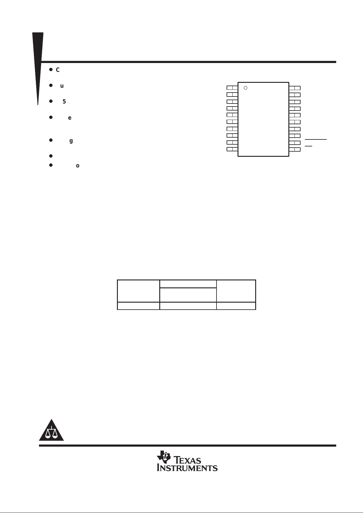
Low-Profile (1.2-mm Max Height), 20-Pin
TSSOP Package
description
The TPS9103 is a highly integrated power supply for depletion-mode GaAs power amplifiers (PA) in cellular
handsets and other wireless communications equipment. Functional integration and low-profile packaging
combine to minimize circuit-board area and component height requirements. The device includes: a p-channel
MOSFET configured as a high-side switch to control the application of power to the P A; a driver for the high-side
switch with a logic-compatible input; a charge pump to provide negative gate-bias voltage; and logic to prevent
turn-on of the high-side switch until gate bias is present. The high-side switch has a typical on-state resistance
of 135 mΩ.
The TPS9103 is available in a 20-pin thin shrink small-outline package (TSSOP) or in chip form. Contact factory
for die sales. The device operates over a junction temperature range of –25°C to 125°C.
AVAILABLE OPTIONS
PACKAGED DEVICE
T
A
TSS0P
(PW)
CHIP FORM
(Y)
–25°C to 85°C TPS9103PWLE TPS9103Y
The PW package is only available left-end taped and reeled
(indicated by the LE suffix on the device type).
Please be aware that an important notice concerning availability, standard warranty, and use in critical applications of
Texas Instruments semiconductor products and disclaimers thereto appears at the end of this data sheet.
1
2
3
4
5
6
7
8
9
10
20
19
18
17
16
15
14
13
12
11
GATE_BIAS
V
CC
C1–
C1+
BATT_IN
BATT_IN
BATT_IN
PGP
PG
GND
V
DD
CLK
BCLK
GND
BATT_OUT
BATT_OUT
BATT_OUT
SW_EN
OSC_EN
EN
PW PACKAGE
(TOP VIEW)
PRODUCTION DATA information is current as of publication date.
Products conform to specifications per the terms of Texas Instruments
standard warranty. Production processing does not necessarily include
testing of all parameters.
Copyright 1996, Texas Instruments Incorporated
TPS9103
POWER SUPPLY FOR GaAs POWER AMPLIFIERS
SLVS131A – OCTOBER 1995 – REVISED JULY 1996
2
POST OFFICE BOX 655303 • DALLAS, TEXAS 75265
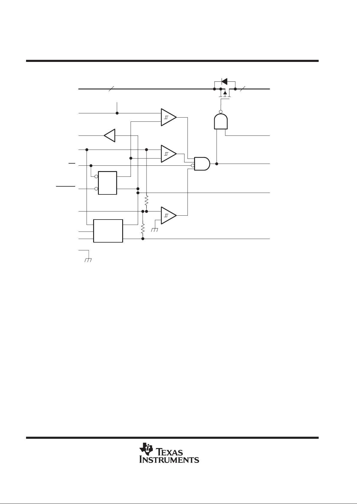
functional block diagram
12
33
REF
+
OSC
Inverting
Charge
Pump
0.6R
5, 6, 7
2
18
20
11
8
10, 17
4
3
14, 15, 16
13
9
19
1
BATT_OUT
SW_EN
PG
CLK
GATE_BIAS
BATT_IN
V
CC
BCLK
V
DD
EN
OSC_EN
PGP
C1+
C1–
GND
V
ref
UVLO
UVDLO
V
CC
PG
Comparator
R
TPS9103
POWER SUPPLY FOR GaAs POWER AMPLIFIERS
SLVS131A – OCTOBER 1995 – REVISED JULY 1996
3
POST OFFICE BOX 655303 • DALLAS, TEXAS 75265
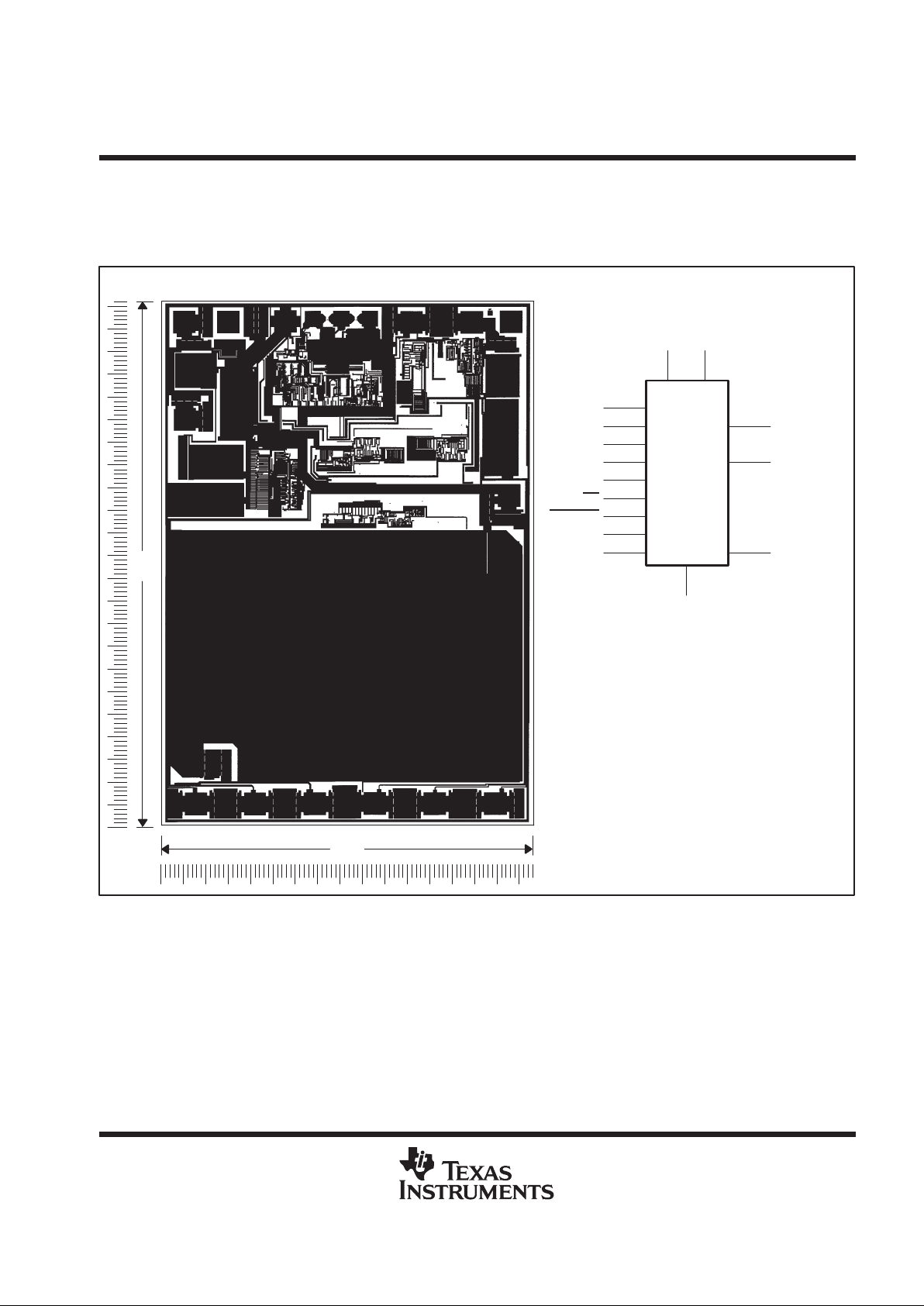
TPS9103Y chip information
This chip, when properly assembled, displays characteristics similar to the TPS9103. Thermal compression or
ultrasonic bonding may be used on the doped-aluminum bonding pads. The chips may be mounted with
conductive epoxy or a gold-silicon preform. Contact factory for die sales.
BONDING PAD ASSIGNMENTS
CHIP THICKNESS: 15 TYPICAL
BONDING PADS: 4 × 4 MINIMUM
TJ max = 150°C
TOLERANCES ARE ±10%.
ALL DIMENSIONS ARE IN MILS.
83
116
(6)(7)
TPS9103Y
C1+
C1–
BATT_IN
PGP
EN
OSC_EN
SW_EN
CLK
GATE_BIAS
BATT_OUT
BCLK
PG
VCCV
DD
202
GND
10, 17
1
14, 15, 16
18
4
3
5, 6, 7
8
9
11
12
13
19
(2)(3)
(1 )
(20)
(19)
(18)
(4)
(5)
(6)
(7)
(17)
(16)
(15)
(14)
(8) (9) (10) (11) (12) (13)
TPS9103
POWER SUPPLY FOR GaAs POWER AMPLIFIERS
SLVS131A – OCTOBER 1995 – REVISED JULY 1996
4
POST OFFICE BOX 655303 • DALLAS, TEXAS 75265
Terminal Functions
TERMINAL
NAME NO.
DESCRIPTION
GATE_BIAS 1 Negative gate-bias output voltage
V
CC
2 Logic supply voltage
C1– 3 External capacitor connection (inverting charge pump)
C1+ 4 External capacitor connection (inverting charge pump)
BATT_IN 5 High-side switch input voltage
BATT_IN 6 High-side switch input voltage
BATT_IN 7 High-side switch input voltage
PGP 8 Program input for power-good threshold
PG 9 Power-good output
GND 10 Ground
EN 11 Chip-enable input
OSC_EN 12 Oscillator-enable input
SW_EN 13 High-side switch enable input
BATT_OUT 14 High-side switch output voltage
BATT_OUT 15 High-side switch output voltage
BATT_OUT 16 High-side switch output voltage
GND 17 Ground
BCLK 18 Buffered clock output
CLK 19 Clock (bidirectional)
V
DD
20 Charge-pump supply voltage

TPS9103
POWER SUPPLY FOR GaAs POWER AMPLIFIERS
SLVS131A – OCTOBER 1995 – REVISED JULY 1996
5
POST OFFICE BOX 655303 • DALLAS, TEXAS 75265
detailed description
high-side switch and driver (BATT_IN, BATT_OUT, SW_EN)
The high-side switch is a p-channel MOSFET with a maximum on-state resistance of 180 mΩ
(V
I(BATT_IN)
= 6 V and VCC = 3.3 V). The driver pulls the gate of the high-side switch to GA TE_BIAS instead of
ground to reduce the MOSFET on-state resistance. Gate breakdown considerations limit the voltage between
BA TT_IN and GATE_BIAS to 15 V. Extremely fast switching times are not required in this application, and the
high-side switch/driver is designed to provide 2 µs maximum switching times with minimum power consumption.
The GaAs depletion-mode MOSFETs in the PA are protected from damage at power-up by internal logic that
inhibits the driver until negative gate bias is available. The control input SW_EN is compatible with 3-V and 5-V
CMOS logic; a logic-high input turns the high-side switch on.
oscillator (OSC_EN
, CLK)
The internal oscillator drives the charge pump at 50 kHz with a nominal duty cycle of 50% when both the EN
and OSC_EN inputs are logic lows. CLK outputs the internal oscillator signal (no buffer). A logic-high input to
OSC_EN
disables the internal oscillator and allows the charge pump to operate from an external clock
connected to CLK. When an external clock with negative overshoot is applied, a Schottky diode must be added
to limit the amplitude of the overshoot.
charge pump (GATE_BIAS, C1+, C1–)
The inverting charge pump generates the negative gate-bias voltage output at GATE_BIAS.
chip enable (EN
)
A logic high on EN
shuts down the internal functions of the TPS9103 and turns the bias system off, reducing
the supply current to less than 10 µA. A low input on EN
causes normal operation to resume.
power good (PG, PGP)
PG output is logic high when GATE_BIAS is in regulation. PG output is logic low when GATE_BIAS is not in
regulation. The high-side switch is disabled and PG is forced to logic low whenever the magnitude of
GATE_BIAS is less than 0.6 × V
DD
. A modified threshold for the power-good function can be achieved by
programming PGP with an external resistor.
undervoltage lockout for V
CC
and V
DD
(UVLO and UVDLO)
Undervoltage lockout prevents operation at supply voltages too low for proper operation. When UVLO or
UVDLO is active, all power-switch drives are forced to the off state and bias is removed from unneeded
functions. Hysteresis is provided to minimize cycling on and off because of source impedance loading when the
supply voltage is close to the threshold.
buffered clock output (BCLK)
The buffered clock output is a driver for an external charge pump. When the optional external charge pump is
not needed, BCLK should be left unconnected. For more details, see the application section.
supply input for inverting charge pump (V
DD
)
V
DD
is the supply voltage for the inverting charge pump. In normal operation, V
DD
is connected to VCC. If the
negative gate-bias needs to be larger than V
CC
(i.e., more negative), then a higher voltage supply needs to be
connected to V
DD
. This can be supplied from an external charge pump driven from BCLK.
TPS9103
POWER SUPPLY FOR GaAs POWER AMPLIFIERS
SLVS131A – OCTOBER 1995 – REVISED JULY 1996
6
POST OFFICE BOX 655303 • DALLAS, TEXAS 75265
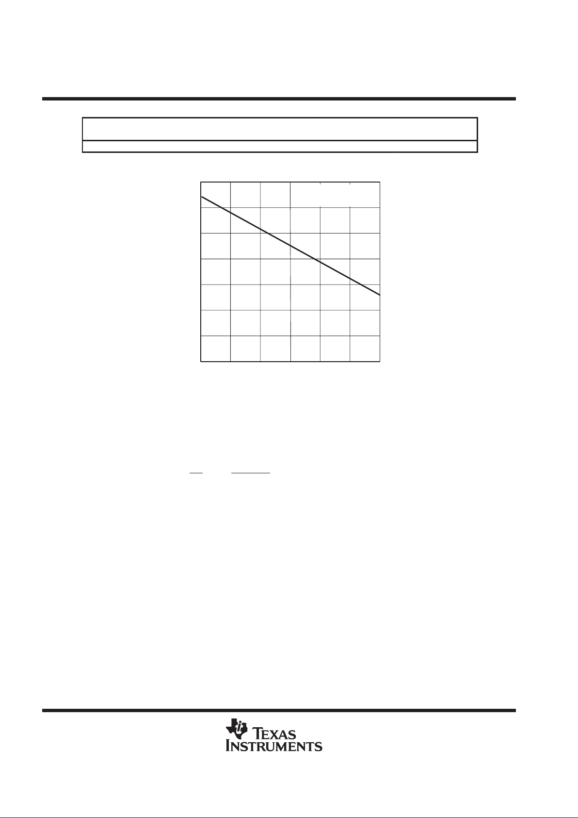
DISSIPATION RATING TABLE
PACKAGE
TA ≤ 25°C
POWER RATING
DERATING FACTOR
ABOVE TA = 25°C
TA = 70°C
POWER RATING
TA = 85°C
POWER RATING
PW 645 mW 6.5 mW/°C 353 mW 255 mW
Maximum values are calculated using a derating factor based on R
θJA
= 154°C/W for the package. These devices are
mounted on an FR4 board with no special thermal considerations.
400
300
100
0
25 35 45 55
– Maximum Continuous Dissipation – mW
500
600
700
65 75 85
200
PW Package
R
θJA
= 154°C/W
P
D
TA – Free-Air Temperature – °C
Figure 1. Dissipation vs Free-Air Temperature
absolute maximum ratings over operating free-air temperature range (unless otherwise noted)
†
High-side switch input voltage range, BATT_IN (see Note 1) –0.3 V to 15 V. . . . . . . . . . . . . . . . . . . . . . . . . . . .
Supply voltage range, V
CC
, VDD –0.3 V to 7 V. . . . . . . . . . . . . . . . . . . . . . . . . . . . . . . . . . . . . . . . . . . . . . . . . . . . .
Differential voltage, |BATT_IN|–|GATE_BIAS| 15 V. . . . . . . . . . . . . . . . . . . . . . . . . . . . . . . . . . . . . . . . . . . . . . . . .
Input voltage range, SW_EN, EN
, CLK, OSC_EN, PG –0.3 V to V
CC
+ 0.3 V. . . . . . . . . . . . . . . . . . . . . . . . . .
GA TE_BIAS –5.5 V. . . . . . . . . . . . . . . . . . . . . . . . . . . . . . . . . . . . . . . . . . . . . . . . . . . . . . . . . . . . . . . . . . . . . . . . . . . .
Output current, PG 5 mA. . . . . . . . . . . . . . . . . . . . . . . . . . . . . . . . . . . . . . . . . . . . . . . . . . . . . . . . . . . . . . . . . . . . . . . .
Output current, BCLK 50 mA. . . . . . . . . . . . . . . . . . . . . . . . . . . . . . . . . . . . . . . . . . . . . . . . . . . . . . . . . . . . . . . . . . . . .
Output current, GATE_BIAS 10 mA. . . . . . . . . . . . . . . . . . . . . . . . . . . . . . . . . . . . . . . . . . . . . . . . . . . . . . . . . . . . . . .
Output current, BATT_OUT 2 A. . . . . . . . . . . . . . . . . . . . . . . . . . . . . . . . . . . . . . . . . . . . . . . . . . . . . . . . . . . . . . . . .
Peak output current, BATT_OUT 4 A. . . . . . . . . . . . . . . . . . . . . . . . . . . . . . . . . . . . . . . . . . . . . . . . . . . . . . . . . . . . .
Maximum external clock frequency, CLK 100 kHz. . . . . . . . . . . . . . . . . . . . . . . . . . . . . . . . . . . . . . . . . . . . . . . . . .
Continuous total power dissipation See Dissipation Rating Table. . . . . . . . . . . . . . . . . . . . . . . . . . . . . . . . . . . . .
Junction temperature range, T
J
–25°C to 150°C. . . . . . . . . . . . . . . . . . . . . . . . . . . . . . . . . . . . . . . . . . . . . . . . . . .
Storage temperature range, T
stg
–65°C to 150°C. . . . . . . . . . . . . . . . . . . . . . . . . . . . . . . . . . . . . . . . . . . . . . . . . .
†
Stresses beyond those listed under “absolute maximum ratings” may cause permanent damage to the device. These are stress ratings only, and
functional operation of the device at these or any other conditions beyond those indicated under “recommended operating conditions” is not
implied. Exposure to absolute-maximum-rated conditions for extended periods may affect device reliability.
NOTES: 1. All voltages are with respect to device GND.
2. Differential voltage calculated: |VImax| + |GATE_BIAS|
TPS9103
POWER SUPPLY FOR GaAs POWER AMPLIFIERS
SLVS131A – OCTOBER 1995 – REVISED JULY 1996
7
POST OFFICE BOX 655303 • DALLAS, TEXAS 75265
recommended operating conditions
MIN NOM MAX UNIT
Input voltage, BATT_IN 3 9 V
Supply voltage, V
CC, VDD
2.7 5.5 V
Output voltage, GATE_BIAS, V
O
–2 –5 V
Continuous output current, GATE_BIAS 0 10 mA
Continuous output current, BATT_OUT 0 2 A
Charge-pump capacitor value at C1+/C1– 0.33 µF
External clock frequency, CLK 25 75 kHz
High-level input voltage, V
IH
2 V
Low-level input voltage, V
IL
SW_EN, EN, OSC_EN, CLK
0.8 V
Input current, I
I
–1 1 µA
Operating junction temperature, T
J
–25 125 °C
electrical characteristics over recommended operating junction temperature range,
BATT_IN = 6 V, V
CC
= V
DD
= 3.3 V, I
O(BATT_OUT)
= 0.5 A, I
O(GATE_BIAS)
= 2 mA,
EN
= OSC_EN = 0 V, SW_EN = VCC, C1 = 0.33 µF (unless otherwise noted)
charge pump
PARAMETER TEST CONDITIONS MIN TYP MAX UNIT
Output voltage –3 –3.10 –3.3 V
Output resistance 95 Ω
high-side switch
PARAMETER TEST CONDITIONS MIN TYP MAX UNIT
TA = 25°C 135 180
TA = –25°C to 85°C 210
D
ran-to-source on-state resistance
TA = 25°C,
V
I(BATT_IN)
= 3 V
160 220
m
Ω
TA = –25°C to 85°C, BATT_IN = 3 V 260
TA = 25°C,
V
I(BATT_IN)
= 9 V,
SW_EN = 0 V 1
Leakage current
TA = 85°C,
V
I(BATT_IN)
= 9 V,
SW_EN = 0 V 10
µ
A
Delay to high-level output SW_EN from 0 to V
CC
0.2 2 µs
Delay to low-level output SW_EN from VCC to 0 0.9 2 µs
oscillator
PARAMETER TEST CONDITIONS MIN TYP MAX UNIT
Frequency VCC = 2.7 V to 5.5 V 35 50 60 kHz
Duty cycle VCC = 2.7 V to 5.5 V 40% 50% 60%
buffered clock output (BCLK)
PARAMETER TEST CONDITIONS MIN TYP MAX UNIT
Output resistance 10 Ω
High-level output voltage I(BCLK) = 30 mA VCC –0.3 V
Low-level output voltage I(BCLK) = 30 mA 0.3 V

TPS9103
POWER SUPPLY FOR GaAs POWER AMPLIFIERS
SLVS131A – OCTOBER 1995 – REVISED JULY 1996
8
POST OFFICE BOX 655303 • DALLAS, TEXAS 75265
power good (PG)
PARAMETER TEST CONDITIONS MIN TYP MAX UNIT
Threshold voltage VDD = 2.7 V to 5.5 V 0.60 × V
DD
V
On-state voltage I
O(PG)
= 500 µA, VCC = 2.7 V to 5.5 V 0.3 V
Off-state voltage I
O(PG)
= –500 µA, VCC = 2.7 V to 5.5 V VCC –0.3 V
Hysteresis 130 mV
power good (PGP)
PARAMETER TEST CONDITIONS MIN TYP MAX UNIT
Input impedance 85 kΩ
undervoltage lockout (UVLO + UVDLO)
PARAMETER TEST CONDITIONS MIN TYP MAX UNIT
Start threshold voltage VCC increasing 2.4 2.7 V
Hysteresis 130 mV
supply current (ICC and IDD)
PARAMETER TEST CONDITIONS MIN TYP MAX UNIT
Standby mode EN = V
CC
1 10 µA
Undervoltage lockout VCC = VDD < 2.3 V 35 50 µA
Operating mode No load 300 500 µA

TPS9103
POWER SUPPLY FOR GaAs POWER AMPLIFIERS
SLVS131A – OCTOBER 1995 – REVISED JULY 1996
9
POST OFFICE BOX 655303 • DALLAS, TEXAS 75265
PARAMETER MEASUREMENT INFORMATION
BATT_IN
BATT_IN
BATT_IN
V
CC
V
DD
C1+
C1–
SW_EN
EN
OSC_EN
GND GND
BATT_OUT
BATT_OUT
BATT_OUT
GATE_BIAS
PG
PGP
CLK
BCLK
C1
0.1 µF
C4
0.1 µF
+
C3
4.7 µF
C2
0.33 µF
10 kΩ
10 kΩ
10 kΩ
V
CC
C5
0.1 µF
C6
4.7 µF
+
I
O(BATT_OUT)
I
O(GATE_BIAS)
I
O(BCLK)
TSP9103
V
I(BATT_IN)
V
CC
5
6
7
2
20
4
3
13
11
12
17 10
14
15
16
1
9
8
19
18
Figure 2. Test Circuit
V
CC
GATE BIAS
4
3
2
1
0
– 1
– 2
– 3
0 5 10 15 20 25 30 35 40 45 50
t – Time – ms
Input and Output Voltage – V
Figure 3. GATE_BIAS Output Voltage Rise Time

TPS9103
POWER SUPPLY FOR GaAs POWER AMPLIFIERS
SLVS131A – OCTOBER 1995 – REVISED JULY 1996
10
POST OFFICE BOX 655303 • DALLAS, TEXAS 75265
PARAMETER MEASUREMENT INFORMATION
IO – GATE_BIAS = 5 mA
VDD = VCC = 5 V
20 mV/div
0 5 10 15 20 25 30 35 40
t – Time – µs
Figure 4. Ripple on GATE_BIAS

TPS9103
POWER SUPPLY FOR GaAs POWER AMPLIFIERS
SLVS131A – OCTOBER 1995 – REVISED JULY 1996
11
POST OFFICE BOX 655303 • DALLAS, TEXAS 75265
TYPICAL CHARACTERISTICS
T ABLE OF GRAPHS
FIGURE
vs Gate-source voltage, dc 5
r
DS(on)
Static drain-source on-state resistance
vs Temperature 6
vs Supply voltage 7
F
osc
Oscillator frequenc
y
vs Temperature
8
p
vs Output current 9
VOOutput voltage
vs CLK frequency 10
V
IT
Threshold voltage vs Temperature 11
pp
vs Supply voltage 12
Supply current (I
CC
+
IDD)
vs Temperature 13
Figure 5
130
110
100
– 12 – 1 1 – 10 – 9
– Static Drain-Source On-State Resistance – m
160
180
STATIC DRAIN-SOURCE ON-STATE RESISTANCE
vs
GATE-SOURCE VOLTAGE,
dc (V
O(GATE_BIAS)
–V
I(BATT_IN)
)
190
– 8 – 7 – 6
170
150
140
120
r
DS(on)
Ω
VGS – Gate-Source Voltage,
dc (V
O
(
GATE_BIAS
)
–V
I(BATT_IN
)
)
Figure 6
120
100
80
60
– 50 – 25 0 25 50
140
160
HIGH-SIDE SWITCH
STATIC DRAIN-SOURCE ON-STATE RESISTANCE
vs
TEMPERATURE
180
75 100 125
T – Temperature – ° C
– Static Drain-Source On-State Resistance – m
r
DS(on)
Ω

TPS9103
POWER SUPPLY FOR GaAs POWER AMPLIFIERS
SLVS131A – OCTOBER 1995 – REVISED JULY 1996
12
POST OFFICE BOX 655303 • DALLAS, TEXAS 75265
TYPICAL CHARACTERISTICS
Figure 7
Figure 9
47
46
2.5 3 3.5 4
48
OSCILLATOR FREQUENCY
vs
SUPPLY VOLTAGE
49
4.5 5 5.5
VCC – Supply Voltage – V
– Oscillator Frequency – kHz
f
osc
IO – Output Current – mA
– 3
– 4
– 5
– 6
0123456
– Output Voltage – V
– 2
– 1
GATE BIAS
OUTPUT VOLTAGE
vs
OUTPUT CURRENT
0
78910
V
O
VCC = 2.7 V
VCC = 3.3 V
VCC = 5 V
Figure 8
T – Temperature – ° C
48
47.5
47
– 50 – 25 0 25 50
48.5
49
OSCILLATOR FREQUENCY
vs
TEMPERATURE
49.5
75 100 125
3.3 V
2.7 V
5 V
– Oscillator Frequency – kHz
f
osc
Figure 10
– 3.15
– 3.2
– 3.25
– 3.3
25 30 35 40 45 50 55
– Output Voltage – V
– 3.1
– 3.05
f – CLK Frequency – kHz
GATE BIAS
OUTPUT VOLTAGE
vs
CLK FREQUENCY
– 3
60 65 70 75
V
O

TPS9103
POWER SUPPLY FOR GaAs POWER AMPLIFIERS
SLVS131A – OCTOBER 1995 – REVISED JULY 1996
13
POST OFFICE BOX 655303 • DALLAS, TEXAS 75265
TYPICAL CHARACTERISTICS
Figure 11
5.5 V
350
300
250
200
– 50 – 25 0 25 50
400
450
SUPPLY CURRENT (ICC + IDD)
vs
TEMPERATURE
500
75 100 125
T – Temperature – ° C
3.3 V
Supply Current (I
CC
+ I
DD
) –
Aµ
Figure 13
2.59
2.57
2.55
– 50 – 25 0 25 50
– Threshold Voltage – V
2.61
2.63
UNDERVOLTAGE LOCKOUT (VCC, VDD)
THRESHOLD VOLTAGE
vs
TEMPERATURE
2.65
75 100 125
V
IT
T – Temperature – ° C
Figure 12
300
250
200
2.7 3.2 3.7 4.2 4.7 5.2 5.7
350
400
SUPPLY CURRENT (ICC + IDD)
vs
SUPPLY VOLTAGE
450
Supply Voltage – V
Supply Current (I
CC
+ I
DD
) –
Aµ

TPS9103
POWER SUPPLY FOR GaAs POWER AMPLIFIERS
SLVS131A – OCTOBER 1995 – REVISED JULY 1996
14
POST OFFICE BOX 655303 • DALLAS, TEXAS 75265
THERMAL INFORMATION
Implementation of integrated circuits in low-profile and fine-pitch packages requires special attention to power
dissipation. Many system-dependent issues such as thermal coupling, airflow, added heat sinks and convection
surfaces, and the presence of other heat-generating components affect the power-dissipation limits of a given
component.
Three basic approaches for enhancing thermal performance are listed below:
D
Improving the power-dissipation capability of the PWB design
D
Improving the thermal coupling of the component to the PWB
D
Introducing airflow in to the system
Using the given R
θJA
for this IC, the maximum power dissipation can be calculated with the equation:
PDmax
+
TJmax*T
A
R
q
JA
For the TPS9103, the power dissipation is in the PMOSFET . To calculate the power, use:
I2
R
where I is the
current through the device and R is the internal resistance as shown in the electrical characteristics table.
For a V
I
of 6 V, the resistance at 85°C is 0.210 Ω. At a current of 2 A, the peak power dissipation is:
PD+
22
0.210+0.84 W
Assuming a duty cycle of 1/8 or 0.125, the average power is:
0.84 W 0.125+0.105 W
The change in temperature is:
∆T = 0.105 W × 154°C/W = 16.2°C
and the junction temperature is:
T
J
= 85°C + 16.2°C =101.2°C

TPS9103
POWER SUPPLY FOR GaAs POWER AMPLIFIERS
SLVS131A – OCTOBER 1995 – REVISED JULY 1996
15
POST OFFICE BOX 655303 • DALLAS, TEXAS 75265
APPLICATION INFORMATION
introduction
Traditionally the RF power amplifier (P A) is powered directly from the battery, with a switching arrangement for
powering down when not in use. GaAs FET PAs require a negative bias voltage that must be present before
the supply is connected, or there is risk of destroying the FET. Logic must be provided to ensure the presence
of the negative bias voltage.
A secondary charge pump is necessary for systems in which the supply voltage is insufficiently high – the
negative bias produced from the charge pump is inadequate. In mobile telephony a second charge pump
(regulated or unregulated) may also be needed, e.g. for varicap diodes/VCOs and some preamplifiers. The
need for larger dynamic range or control-voltage range can become critical in certain applications.
the TPS9103 approach
The TPS9103 integrates a P-channel MOSFET high-side switch together with a selectable oscillator and charge
pump for the GaAs FET power-amplifier gate bias, which is monitored.
Complete precautions are taken to ensure that the P A supply is not enabled unless the gate bias is present while
V
CC
and VDD are also good. This protects the PA from inadvertent damage–without a major system size/cost
increase.
The bias regulation monitor is flexible, accommodating both fixed and programmable approaches. The fixed
resistors, provided internally , set the trip voltage to –0.6 x V
DD
. If V
DD
is 5 V , then the trip voltage is –3 V . Should
another value be preferred, it can be set by applying voltage divider to PGP. See the section “dimensioning the
external voltage divider” for more details.
The charge pump clock is also flexible. The on-chip oscillator runs at a nominal 50 kHz, or alternatively an
external oscillator can be connected to CLK. When an external clock is used, OSC_EN
should be taken high
to disable the oscillator. When OSC_EN
is low and the on-chip oscillator is used, CLK provides an unbuffered
clock output.
The circuit provides for a secondary charge pump driver. The buffered BCLK output can be used (with four
external components) to provide a higher supply , both for those system functions that require it and for those
GaAs PAs that need a more negative bias than is made possible by inverting the existing supply. This is
facilitated by use of single-cell Li-ion batteries.
Figure 14 shows the TPS9103 in a typical application.

TPS9103
POWER SUPPLY FOR GaAs POWER AMPLIFIERS
SLVS131A – OCTOBER 1995 – REVISED JULY 1996
16
POST OFFICE BOX 655303 • DALLAS, TEXAS 75265
APPLICATION INFORMATION
BATT_IN
BATT_IN
BATT_IN
SW_EN
C1+
C1–
V
DD
EN
OSC_EN
GND GND
BATT_OUT
BATT_OUT
BATT_OUT
GATE_BIAS
PG
PGP
CLK
BCLK
C1
0.1 µF
C4
0.1 µF
+
C3
4.7 µF
C2
0.33 µF
C5
0.1 µF
C6
4.7 µF
+
PA Drain
TSP9103
Battery
4 V to 8 V
V
CC
3.3 V
5
6
7
13
4
3
20
11
12
17 10
14
15
16
1
9
8
19
18
2
V
CC
XMIT
PA Gate–3 V
Figure 14. Typical Application

TPS9103
POWER SUPPLY FOR GaAs POWER AMPLIFIERS
SLVS131A – OCTOBER 1995 – REVISED JULY 1996
17
POST OFFICE BOX 655303 • DALLAS, TEXAS 75265
APPLICATION INFORMATION
capacitors of the internal inverting charge pump (see Figure 15)
This charge pump inverts the voltage at V
DD
and provides a negative output voltage at GATE_BIAS.
Charge
Pump
GATE_BIAS
C6
C +
C –
C2
TPS9103
+
Figure 15. Internal Inverting Charge Pump
The output capacitor C6 limits the voltage ripple at GATE_BIAS:
V
Ripple
+
I
O(GATE_BIAS)
C6 f
With a capacitor C6 of 4.7 µF and an output current of 10 mA, the voltage ripple at GATE_BIAS is 42 mV.
The capacitor C2 can be calculated using an equivalent resistance method:
R
equivalent
+
1
C2 f
Using 0.33 µF for C2, the equivalent resistance is:
R
equivalent
+
1
0.33mF 50 kHz
+
60.6
W
Add the internal resistance of the switches (35 Ω) to get a total resistance seen by the current:
R
TOTAL
+60)35+95W
With a total resistance of 95 Ω and 10 mA flowing through it, a voltage drop of 0.95 V occurs. With 5 V on V
DD
,
the output is –4.05 V with a 42 mV ripple.
The capacitors should have a low equivalent series resistance (ESR) to maintain low ripple and low noise.
Careful layout is required. In most instances it is advisable to add a small decoupling capacitor C5 close to the
GA TE_BIAS. An additional 0.1-µF capacitor at other locations may be necessary if the power amplifier is located
away from the TPS9103.

TPS9103
POWER SUPPLY FOR GaAs POWER AMPLIFIERS
SLVS131A – OCTOBER 1995 – REVISED JULY 1996
18
POST OFFICE BOX 655303 • DALLAS, TEXAS 75265
APPLICATION INFORMATION
dimensioning of the external charge pump
For systems in which the bias voltage requirement is not met by inverting the power rail, the BCLK output can
be used (with four passive components) to generate a higher V
DD.
The higher voltage is then inverted as before
to produce the bias voltage. This voltage is also available for other parts of the main circuitry (see Figure 16).
With the TPS9103, an external charge pump could be used to increase the voltage at V
DD
, thereby deriving a
higher negative voltage at GATE_BIAS than would otherwise be available.
1
+
C8
V
DD
D1
D2
V
CC
V
BCLK
C7
Figure 16. External Charge Pump
When BCLK is low, node 1 charges up to V
CC
– V
diode
. When BCLK goes high, node 1 is 2 VCC – V
diode
. The
capacitor C8 charges up to 2 V
CC
– 2 V
diode
. This voltage can then be connected to VDD.
The magnitude of V
ripple
of V
DD
is determined by the value of C8. Capacitor value must be large enough that
the discharge during one period is not as great as the maximum voltage variation allowable. The discharge of
C8 depends on the load current.
C8
+
I
O(GATE_BIAS)
V
ripple f
With a supply voltage of V
CC
= 3.3 V, a maximum voltage variation (V
ripple
) of 2% = 66 mV and a load of
I
CC
= 10 mA, the value of C8 is 3 µF. A 4.7 µF meets this requirement.
The capacitance of C7 can be calculated using an equivalent resistance method:
R
equivalent
+
1
C7 f
Using 0.22 µF for C7, the equivalent resistance is:
R
equivalent
+
1
0.22mF 50 kHz
+90W
Add the equivalent resistance to the internal resistance of the switch (10 Ω):
R
TOTAL
= 90 + 10 = 100 Ω
With a total resistance of 100 Ω and with 10 mA flowing through it, a voltage drop of 1 V occurs. Thus with 3.3
V on V
CC
the output is 4.2 V with a 42-mV ripple.
Care must be taken that the maximum voltages are not exceeded when using BCLK as a charge pump (see
Figure 17).

TPS9103
POWER SUPPLY FOR GaAs POWER AMPLIFIERS
SLVS131A – OCTOBER 1995 – REVISED JULY 1996
19
POST OFFICE BOX 655303 • DALLAS, TEXAS 75265
APPLICATION INFORMATION
BATT_IN
BATT_IN
BATT_IN
SW_EN
C1+
C1–
EN
OSC_EN
GND GND
BATT_OUT
BATT_OUT
BATT_OUT
GATE_BIAS
V
DD
PGP
CLK
BCLK
C1
0.1 µF
C4
0.1 µF
+
C3
4.7 µF
C2
0.33 µF
C5
0.1 µF
C6
4.7 µF
+
PA Drain
TSP9103
Battery
4 V to 8 V
V
CC
3.3 V
5
6
7
13
4
3
11
12
17 10
14
15
16
1
8
19
20
18
2
V
CC
XMIT
PA Gate–3 V
C7
0.22 µF
PG
9
+
C8
4.7 µF
Figure 17. TPS9103 Configured With External Charge Pump

TPS9103
POWER SUPPLY FOR GaAs POWER AMPLIFIERS
SLVS131A – OCTOBER 1995 – REVISED JULY 1996
20
POST OFFICE BOX 655303 • DALLAS, TEXAS 75265
dimensioning the external voltage divider
Drain voltage should only be applied to the power amplifier when the complete negative voltage from the
GATE_BIAS output is provided to the gate of the GaAs power amplifier. For that reason there is an internal
voltage divider R/0.6R and a PG comparator in the TPS9103 (see Figure 15). When the voltage at the inverting
input of the comparator reaches zero, the output goes high and the high-side MOSFET switches on, provided
a SW_EN high signal is applied. For example, when the supply voltage at V
DD
is 5 V, the high-side switch is
switched on when the voltage at GATE_BIAS reaches –3 V.
This trip point can be changed to another value by using an external voltage divider connected between V
DD
,
GATE_BIAS, and PGP. The resistor values should be low enough to minimize the error that is present when
the internal resistor values (typ R = 100 kΩ ± 30%) are taken into consideration. Therefore, the external resistor
values, R1 and R2, are chosen within the 10-kΩ range.
R
0.6 R
PG Comparator
TPS9103
V
DD
PGP
GATE_BIAS
R1
R2
Figure 18. External Voltage Divider for Setting the Trip Point
R1 = 10 kΩ. The value of R2 can then be calculated using:
R2
+
*
0.6 R R1 V
trip
0.6 VDD [R1)R])
V
trip
R1
where V
DD
= supply voltage, and V
trip
= chosen value to trip PG comparator.
The values of the internal resistor can vary about 30%, and can move the trip point. In a worst-case condition,
with a resistor variation of 30%, the shifting of the trip point can be calculated to:
D
V
trip_point
+
VDD
ǒ
R1)1.3 R
R1
0.6 R2
R2)0.78 R
*
R1)R
R1
0.6 R2
R2)0.6 R
Ǔ

TPS9103
POWER SUPPLY FOR GaAs POWER AMPLIFIERS
SLVS131A – OCTOBER 1995 – REVISED JULY 1996
21
POST OFFICE BOX 655303 • DALLAS, TEXAS 75265
MECHANICAL DATA
PW (R-PDSO-G**) PLASTIC SMALL-OUTLINE PACKAGE
4040064/D 10/95
14 PIN SHOWN
Seating Plane
0,10 MIN
1,20 MAX
1
A
7
14
0,19
4,50
4,30
8
6,10
6,70
0,32
0,75
0,50
0,25
Gage Plane
0,15 NOM
0,65
M
0,13
0°–8°
0,10
PINS **
A MIN
A MAX
DIM
2,90
3,10
8
4,90
5,10
14
6,60
6,404,90
5,10
16
7,70
20
7,90
24
9,60
9,80
28
NOTES: A. All linear dimensions are in millimeters.
B. This drawing is subject to change without notice.
C. Body dimensions do not include mold flash or protrusion not to exceed 0,15.
D. Falls within JEDEC MO-153

IMPORTANT NOTICE
T exas Instruments and its subsidiaries (TI) reserve the right to make changes to their products or to discontinue
any product or service without notice, and advise customers to obtain the latest version of relevant information
to verify, before placing orders, that information being relied on is current and complete. All products are sold
subject to the terms and conditions of sale supplied at the time of order acknowledgement, including those
pertaining to warranty, patent infringement, and limitation of liability.
TI warrants performance of its semiconductor products to the specifications applicable at the time of sale in
accordance with TI’s standard warranty. Testing and other quality control techniques are utilized to the extent
TI deems necessary to support this warranty. Specific testing of all parameters of each device is not necessarily
performed, except those mandated by government requirements.
CERT AIN APPLICATIONS USING SEMICONDUCTOR PRODUCTS MAY INVOLVE POTENTIAL RISKS OF
DEATH, PERSONAL INJURY, OR SEVERE PROPERTY OR ENVIRONMENTAL DAMAGE (“CRITICAL
APPLICATIONS”). TI SEMICONDUCTOR PRODUCTS ARE NOT DESIGNED, AUTHORIZED, OR
WARRANTED TO BE SUITABLE FOR USE IN LIFE-SUPPORT DEVICES OR SYSTEMS OR OTHER
CRITICAL APPLICATIONS. INCLUSION OF TI PRODUCTS IN SUCH APPLICA TIONS IS UNDERST OOD TO
BE FULLY AT THE CUSTOMER’S RISK.
In order to minimize risks associated with the customer’s applications, adequate design and operating
safeguards must be provided by the customer to minimize inherent or procedural hazards.
TI assumes no liability for applications assistance or customer product design. TI does not warrant or represent
that any license, either express or implied, is granted under any patent right, copyright, mask work right, or other
intellectual property right of TI covering or relating to any combination, machine, or process in which such
semiconductor products or services might be or are used. TI’s publication of information regarding any third
party’s products or services does not constitute TI’s approval, warranty or endorsement thereof.
Copyright 1998, Texas Instruments Incorporated
 Loading...