

Datasheet TPS79401, TPS79418, TPS79425, TPS79428, TPS79430 Datasheet (TEXAS INSTRUMENTS)
...Page 1
www.ti.com
OUT
NC − No internal connection
1
2
3
4
5
DCQ PACKAGE
NR
OUT
GND
IN
EN
2
1
3
4
7
8
6
5
NC
FB
NR
IN
NC
EN
GND
SOT223-6
(TOP VIEW)
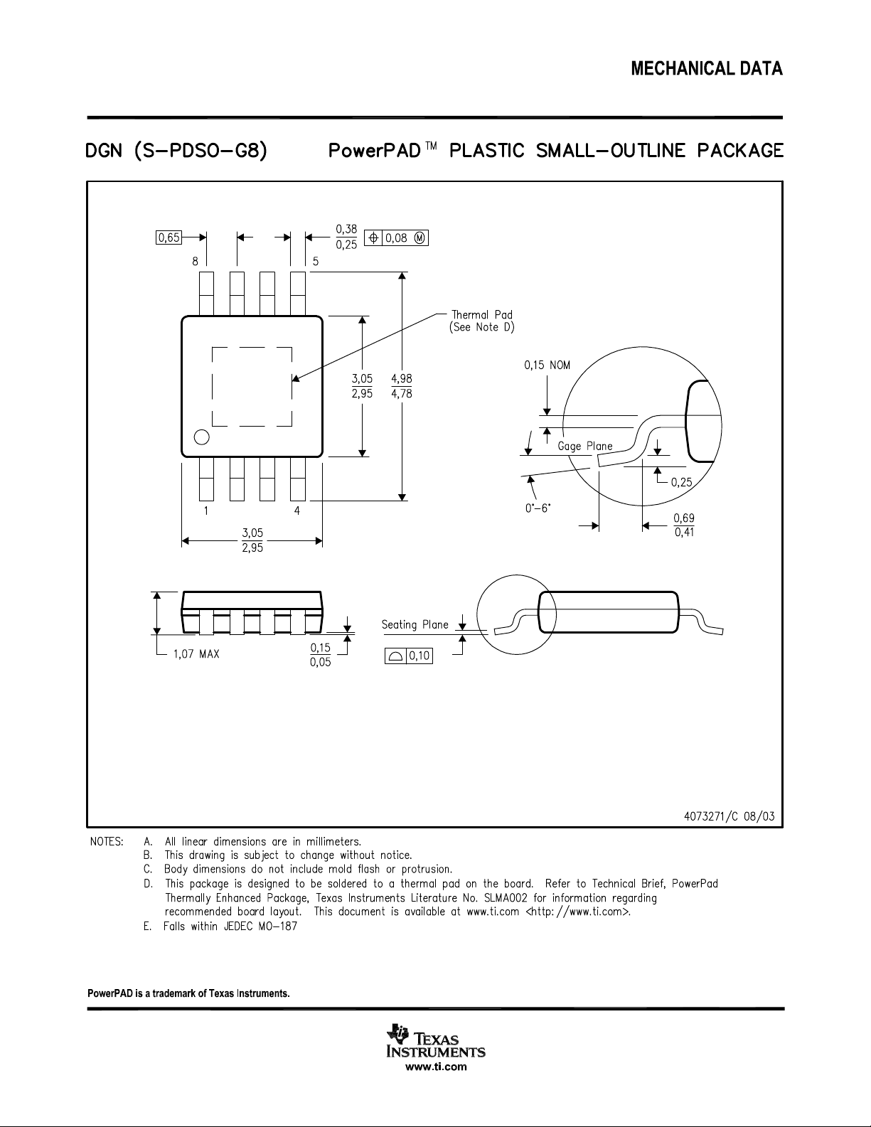
DGN PACKAGE
MSOP PowerPAD
(TOP VIEW)
I
OUT
= 10 mA
I
OUT
= 250 mA
VIN = 4.3 V,
V
OUT
= 3.3 V,
CIN = 1 µF,
C
OUT
= 10 µF,
CNR = 0.01 µF
40
20
10
10 100 1 k 10 k
Ripple Rejection (dB)
60
70
Frequency (Hz)
TPS79433
RIPPLE REJECTION
vs
FREQUENCY
90
100 k 1 M 10 M
0
30
50
80
0
0.05
0.10
0.15
0.20
0.25
0.30
0.35
I
OUT
= 250 mA
I
OUT
= 1 mA
C
OUT
= 2.2 µF,
CNR = 0.1 µF,
VIN = 3.8 V
TPS79428
OUTPUT SPECTRAL NOISE DENSITY
vs
FREQUENCY
Frequency (Hz)
100 1000 10000 100000
6
GND
Output Spectral Noise Density (µV/√Hz)
查询TPS79401供应商
ULTRALOW-NOISE, HIGH PSRR, FAST RF 250-mA LOW-DROPOUT LINEAR
FEATURES DESCRIPTION
• 250-mA Low-Dropout Regulator With Enable
• Available in 1.8 V, 2.5 V, 2.8 V, 3 V, 3.3 V, and
Adjustable (1.2 V to 5.5 V)
• High PSRR (60 dB at 10 kHz)
• Ultralow Noise (32 µVrms, TPS79428)
• Fast Start-Up Time (50 µs)
• Stable With a 2.2-µF Ceramic Capacitor
• Excellent Load/Line Transient Response
• Very Low Dropout Voltage (155 mV at Full
Load)
• Available in MSOP-8 and SOT223-6 Packages
APPLICATIONS
• RF: VCOs, Receivers, ADCs
• Audio
• Bluetooth™, Wireless LAN
• Cellular and Cordless Telephones
• Handheld Organizers, PDAs
TPS79401, TPS79418
TPS79425, TPS79428
TPS79430, TPS79433
SLVS349D – NOVEMBER 2001 – REVISED OCTOBER 2004
REGULATORS
The TPS794xx family of low-dropout (LDO) linear
voltage regulators features high power-supply rejection ratio (PSRR), ultralow-noise, fast start-up, and
excellent line and load transient responses in small
outline, MSOP-8 PowerPAD™ and SOT223-6 packages. Each device in the family is stable with a small
2.2-µF ceramic capacitor on the output. The family
uses an advanced, proprietary BiCMOS fabrication
process to yield extremely low dropout voltages (e.g.,
155 mV at 250 mA). Each device achieves fast
start-up times (approximately 50 µs with a 0.001-µF
bypass capacitor) while consuming low quiescent
current (170 µA typical). Moreover, when the device
is placed in standby mode, the supply current is
reduced to less than 1 µA. The TPS79428 exhibits
approximately 32 µV
2.8 V output with a 0.1-µF bypass capacitor. Applications with analog components that are
noise-sensitive, such as portable RF electronics,
benefit from the high PSRR and low noise features as
well as the fast response time.
of output voltage noise at
RMS
Bluetooth is a trademark of Bluetooth SIG, Inc.
PowerPAD is a trademark of Texas Instruments.
All other trademarks are the property of their respective owners.
PRODUCTION DATA information is current as of publication date.
Products conform to specifications per the terms of the Texas
Instruments standard warranty. Production processing does not
necessarily include testing of all parameters.
Please be aware that an important notice concerning availability, standard warranty, and use in critical applications of Texas
Instruments semiconductor products and disclaimers thereto appears at the end of this data sheet.
Copyright © 2001–2004, Texas Instruments Incorporated
Page 2
www.ti.com
TPS79401, TPS79418
TPS79425, TPS79428
TPS79430, TPS79433
SLVS349D – NOVEMBER 2001 – REVISED OCTOBER 2004
This integrated circuit can be damaged by ESD. Texas Instruments recommends that all integrated
circuits be handled with appropriate precautions. Failure to observe proper handling and installation
procedures can cause damage.
ESD damage can range from subtle performance degradation to complete device failure. Precision
integrated circuits may be more susceptible to damage because very small parametric changes could
cause the device not to meet its published specifications.
PRODUCT VOLTAGE PACKAGE T
MSOP-8 AXL
TPS79401 Adjustable
SOT223-6 PS79401
MSOP-8 AXM
TPS79418 1.8 V
SOT223-6 PS79418
MSOP-8 AYB
TPS79423 2.5 V
SOT223-6 PS79425
MSOP-8 AYC
TPS79428 2.8 V
SOT223-6 PS79428
MSOP-8 AYD
TPS79430 3 V
SOT223-6 PS79430
MSOP-8 AYE
TPS79433 3.3 V
SOT223-6 PS79433
ORDERING INFORMATION
J
-40 ° C to 125 ° C
SYMBOL PART NUMBER
TRANSPORT MEDIA,
QUANTITY
TPS79401DGNR Tape and Reel, 2500
TPS79401DGNT Tape and Reel, 250
TPS79401DCQR Tape and Reel, 2500
TPS79401DCQ Tube, 78
TPS79418DGNR Tape and Reel, 2500
TPS79418DGNT Tape and Reel, 250
TPS79418DCQR Tape and Reel, 2500
TPS79418DCQ Tube, 78
TPS79425DGNR Tape and Reel, 2500
TPS79425DGNT Tape and Reel, 250
TPS79425DCQR Tape and Reel, 2500
TPS79425DCQ Tube, 78
TPS79428DGNR Tape and Reel, 2500
TPS79428DGNT Tape and Reel, 250
TPS79428DCQR Tape and Reel, 2500
TPS79428DCQ Tube, 78
TPS79430DGNR Tape and Reel, 2500
TPS79430DGNT Tape and Reel, 250
TPS79430DCQR Tape and Reel, 2500
TPS79430DCQ Tube, 78
TPS79433DGNR Tape and Reel, 2500
TPS79433DGNT Tape and Reel, 250
TPS79433DCQR Tape and Reel, 2500
TPS79433DCQ Tube, 78
2
Page 3
www.ti.com
θJA
SOT223
SOT223
4in2 Top Side Only
0.5in2 Top Side Only
53°C/W
110°C/W
1
2
CONDITIONS PACKAGE PCB AREA
Condition 1
Condition 2
3
2
1
0
0 25 50 75
4
5
6
100 125 150
T
A
(°C)
P
D
(W)
TPS79401, TPS79418
TPS79425, TPS79428
TPS79430, TPS79433
SLVS349D – NOVEMBER 2001 – REVISED OCTOBER 2004
ABSOLUTE MAXIMUM RATINGS
over operating temperature range unless otherwise noted
VINrange -0.3 V to 6 V
V
range -0.3 V to VIN+ 0.3 V
EN
V
range -0.3 V to 6 V
OUT
Peak output current Internally limited
ESD rating, HBM 2 kV
ESD rating, CDM 500 V
Continuous total power dissipation See Dissipation Ratings Table
Junction temperature range, T
Storage temperature range, T
J
stg
(1) Stresses beyond those listed under absolute maximum ratings may cause permanent damage to the device. These are stress ratings
only, and functional operation of the device at these or any other conditions beyond those indicated under recommended operating
conditions is not implied. Exposure to absolute-maximum-rated conditions for extended periods may affect device reliability.
PACKAGE DISSIPATION RATINGS
PACKAGE R
DGN 150 8.21 49.97 2.50 W 1.60 W 1.30 W
AIR FLOW TA≤ 25 ° C TA= 70 ° C TA= 85 ° C
(CFM) POWER RATING POWER RATING POWER RATING
θ JC
0 8.47 55.09 2.27 W 1.45 W 1.18 W
250 8.20 48.10 2.60 W 1.66 W 1.35 W
(1)
( ° C/W) R
VALUE
-40 ° C to 150 ° C
-65 ° C to 150 ° C
( ° C/W)
θ JA
Figure 1. SOT223 Power Dissipation
3
Page 4
www.ti.com
TPS79401, TPS79418
TPS79425, TPS79428
TPS79430, TPS79433
SLVS349D – NOVEMBER 2001 – REVISED OCTOBER 2004
ELECTRICAL CHARACTERISTICS
Over recommended operating temperature range (T
C
= 10µF, C
OUT
V
Input voltage
IN
I
Continuous output current 0 250 mA
OUT
V
Internal reference TPS79401 TJ= 25 ° C 1.220 1.225 1.230 V
FB
V
Output voltage range TPS79401 V
OUT
Accuracy
Output voltage line regulation
( ∆ V
OUT
Load regulation ( ∆ V
Dropout voltage
VIN= V
Output current limit V
Ground pin current 0 µA < I
Shutdown current
FB pin current V
Power-supply ripple
rejection
Output noise voltage (TPS79428) µV
Time, start-up (TPS79428) RL- 14 Ω , C
High-level enable input voltage 2.7 V < VIN< 5.5 V 1.7 V
Low-level enable input voltage 2.7 V < VIN< 5.5 V 0 0.7 V
EN pin current V
UVLO threshold V
UVLO hysteresis 100 mV
= 0.01 µF, unless otherwise noted. Typical values are at 25 ° C.
NR
PARAMETER TEST CONDITIONS MIN TYP MAX UNIT
(1)
(1)
%/ ∆ VIN)
OUT(nom)
(1)
(2)
- 0.1 V
%/ ∆ I
OUT
) 0 µA < I
OUT
TPS79428 I
TPS79430 I
TPS79433 I
(3)
V
OUT
V
OUT
OUT
OUT
OUT
OUT
V
EN
FB
f = 100 Hz I
TPS79428 f = 10 kHz I
f = 100 kHz I
BW = 100 Hz to 100
kHz, I
EN
CC
= -40 ° C to 125 ° C), V
J
EN
= VIN, V
= V
IN
OUT(nom)
+ 1 V
2.7 5.5 V
FB
+ 1 V ≤ VIN≤ 5.5 V 0 mA ≤ I
≤ 250 mA -3.0 +3.0 %
OUT
+ 1 V < VIN≤ 5.5 V 0.05 0.12 %/V
< 250 mA 10 mV
OUT
= 250 mA 155 210
= 250 mA 155 210 mV
= 250 mA 145 200
= 0 V 925 mA
< 250 mA 170 220 µA
OUT
= 0 V 2.7 V < VIN< 5.5 V 0.07 1 µA
= 1.8 V 1 µA
= 250 mA 65
OUT
= 250 mA 60 dB
OUT
= 250 mA 40
OUT
C
= 0.001 µF 55
NR
C
= 0.0047 µF 36
= 250 mA
OUT
= 1 µF C
OUT
NR
C
= 0.01 µF 33
NR
C
= 0.1 µF 32
NR
C
= 0.001 µF 50
NR
= 0.0047 µF 70 µs
NR
C
= 0.01 µF 100
NR
= 0 1 1 µA
rising 2.25 2.65 V
(1)
, I
= 1mA,
OUT
5.5 - V
V
DO
RMS
V
IN
(1) Minimum VINis 2.7 V or V
(2) Dropout is not measured for the TPS79418 and TPS79425 since minimum VIN= 2.7 V.
(3) For adjustable versions, this applies only after VINis applied; then V
+ VDO, whichever is greater.
OUT
transitions high to low.
EN
4
Page 5
www.ti.com
_
+
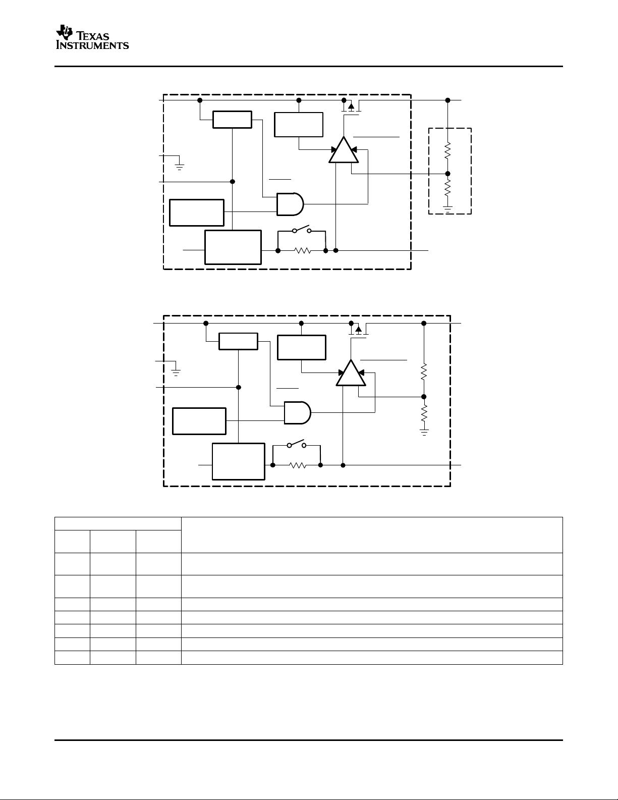
Thermal
Shutdown
Bandgap
Reference
1.225 V
V
IN
Current
Sense
R2
IN
GND
EN
OUT
SHUTDOWN
V
ref
UVLO
ILIM
External to
the Device
FB
R1
UVLO
250 kΩ
NR
(1)
(1) Not Available on DCQ (SOT223) options.
Quickstart
_
+
Thermal
Shutdown
V
IN
Current
Sense
R1
R2
IN
GND
EN
OUT
SHUTDOWN
V
ref
UVLO
ILIM
Bandgap
Reference
1.225 V
UVLO
250 kΩ
NR
Quickstart
R2 = 40k
FUNCTIONAL BLOCK DIAGRAM—ADJUSTABLE VERSION
FUNCTIONAL BLOCK DIAGRAM—FIXED VERSION
TPS79401, TPS79418
TPS79425, TPS79428
TPS79430, TPS79433
SLVS349D – NOVEMBER 2001 – REVISED OCTOBER 2004
TERMINAL
NAME
NR 4 5 Connecting an external capacitor to this pin bypasses noise generated by the internal bandgap. This
EN 6 1 The EN terminal is an input which enables or shuts down the device. When EN goes to a logic high, the
FB 3 5 This terminal is the feedback input voltage for the adjustable device.
GND 5, PAD 3 Regulator ground.
IN 8 2 Unregulated input to the device.
NC 2, 7 No internal connection.
OUT 1 4 Output of the regulator.
DGN DCQ
(MSOP) (SOT223)
Terminal Functions
DESCRIPTION
improves power-supply rejection and reduces output noise.
device will be enabled. When the device goes to a logic low, the device is in shutdown mode.
5
Page 6

www.ti.com
150
155
160
165
170
175
180
185
190
I
OUT
= 1 mA
VIN = 3.8 V,
C
OUT
= 10 µF
T
J
(°C)
I
OUT
= 250 mA
−40−25 −10 5 20 35 50 65 80 95 110 125
I
GND
(µA)
3.250
3.255
3.260
3.265
3.270
3.275
3.280
3.285
3.290
0 50 100 200 250
(V)V
OUT
I
OUT
(mA)
2.765
2.770
2.775
2.780
2.785
2.790
2.800
−40−25−10 5 20 35 50 65 80 95 110 125
T
J
(°C)
(V)V
OUT
2.795
I
OUT
= 1 mA
I
OUT
= 200 mA
VIN = 3.8 V
C
OUT
= 10 µF
0
0.05
0.10
0.15
0.20
0.25
0.30
0.35
I
OUT
= 250 mA
I
OUT
= 1 mA
C
OUT
= 10 µF,
CNR = 0.1 µF,
VIN = 3.8 V
Frequency (Hz)
100 1000 10000 100000
Output Spectral Noise Density (µV/√Hz)
0
0.05
0.10
0.15
0.20
0.25
0.30
0.35
I
OUT
= 250 mA
I
OUT
= 1 mA
C
OUT
= 2.2 µF,
CNR = 0.1 µF,
VIN = 3.8 V
Frequency (Hz)
100 1000 10000 100000
Output Spectral Noise Density (µV/√Hz)
0
0.2
0.4
0.6
0.8
1.2
1.4
1.6
100 1000 10000 100000
C
OUT
= 10 µF,
I
OUT
= 250 mA
VIN = 3.8 V
Frequency (Hz)
CNR = 0.1 µF
CNR = 0.01 µF
CNR = 0.0047 µF
CNR = 0.001 µF
1.0
1.8
Output Spectral Noise Density (µV/√Hz)
0
10
20
30
40
50
60
0.001 0.0047 0.1
C
NR
(µF)
0.01
I
OUT
= 250 mA,
C
OUT
= 10 µF
RMS Output Noise (µV
RMS
)
0
50
100
150
200
250
T
J
(°C)
−40−25 −10 5 20 35 50 65 80 95 110 125
I
OUT
= 1 mA
I
OUT
= 250 mA
VIN = 3.8 V,
C
OUT
= 10 µF
V
DO
(mV)
0.100
0.020
10 100 1 k 10 k
1
10
100 k 1 M 10 M
I
OUT
= 1 mA
I
OUT
= 250 mA
VIN = 4.3 V,
C
OUT
= 10 µF,
Frequency (Hz)
Z
O
, Output Impedance (Ω)
TPS79401, TPS79418
TPS79425, TPS79428
TPS79430, TPS79433
SLVS349D – NOVEMBER 2001 – REVISED OCTOBER 2004
TYPICAL CHARACTERISTICS
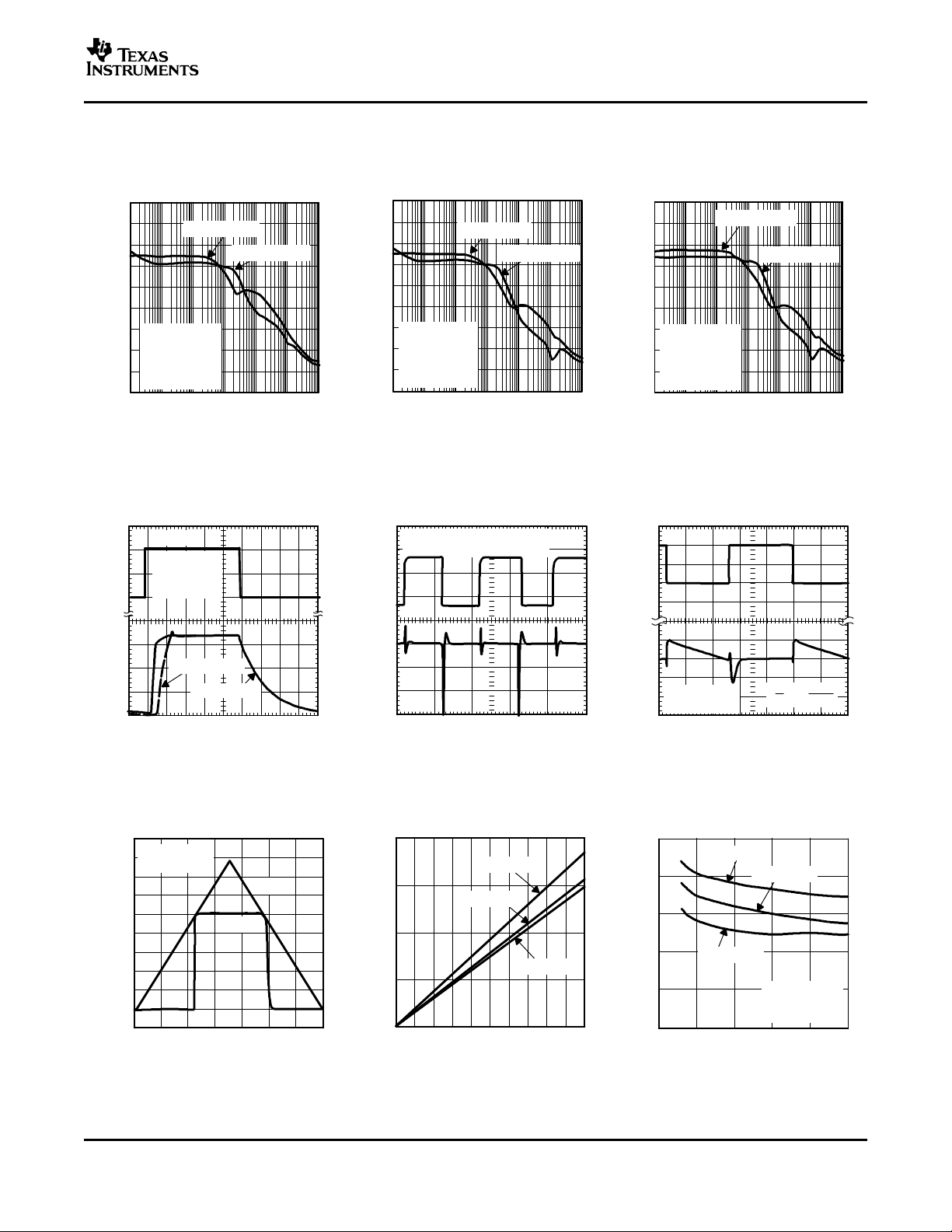
TPS79433 OUTPUT VOLTAGE TPS79428 OUTPUT VOLTAGE TPS79428 GROUND CURRENT
vs vs vs
OUTPUT CURRENT JUNCTION TEMPERATURE JUNCTION TEMPERATURE
Figure 2. Figure 3. Figure 4.
TPS79428 OUTPUT SPECTRAL TPS79428 OUTPUT SPECTRAL TPS79428 OUTPUT SPECTRAL
NOISE DENSITY NOISE DENSITY NOISE DENSITY
vs vs vs
FREQUENCY FREQUENCY FREQUENCY
TPS79428 ROOT MEAN SQUARED
6
Figure 5. Figure 6. Figure 7.
OUTPUT NOISE TPS79433 OUTPUT IMPEDANCE TPS79428 DROPOUT VOLTAGE
vs vs vs
C
NR
FREQUENCY JUNCTION TEMPERATURE
Figure 8. Figure 9. Figure 10.
Page 7
www.ti.com
I
OUT
= 10 mA
I
OUT
= 250 mA
VIN = 4.3 V,
V
OUT
= 3.3 V,
CIN = 1 µF,
C
OUT
= 2.2 µF,
CNR = 0.01 µF
40
20
10
10 100 1 k 10 k
60
70
Frequency (Hz)
90
100 k 1 M 10 M
0
30
50
80
Ripple Rejection (dB)
I
OUT
= 10 mA
I
OUT
= 250 mA
VIN = 4.3 V,
V
OUT
= 3.3 V,
CIN = 1 µF,
C
OUT
= 10 µF,
CNR = 0.01 µF
40
20
10
10 100 1 k 10 k
Ripple Rejection (dB)
60
70
Frequency (Hz)
90
100 k 1 M 10 M
0
30
50
80
I
OUT
= 10 mA
I
OUT
= 250 mA
VIN = 4.3 V,
V
OUT
= 3.3 V,
CIN = 1 µF,
C
OUT
= 2.2 µF,
CNR = 0.1 µF
40
20
10
10 100 1 k 10 k
60
70
Frequency (Hz)
90
100 k 1 M 10 M
0
30
50
80
Ripple Rejection (dB)
0
250
−50
0
50
0 30 60 90 120 150 180 210
Time (µs)
VIN = 4.3 V,
C
OUT
= 10 µF
di
dt
0.02A
s
I
OUT
(mA)∆V
OUT
(mV)
V_Enable
3
Time (µs)
0 24016080 320 400 560480 640 720 800
1
2
0
0
2
4
CNR = 0.0047 µF
VIN = 4.3 V,
V
OUT
= 3.3 V,
I
OUT
= 250 mA,
C
OUT
= 2.2 µF
CNR = 0.001 µF
V
OUT
, V
EN
(V)
Time (µs)
−30
−20
−10
0
10
4.5
5.0
5.5
6.0
0 100 200 300 400 500
I
OUT
= 250 mA,C
OUT
= 10 µF,
CNR = 0.1 µF, dv/dt = 1 V/µs
V
IN
(V)∆V
OUT
(mV)
0
50
100
150
200
0 250
TA = 125°C
TA = 25°C
TA = −40°C
I
OUT
(mA)
25 50 75 100 125 150 175 200 225
V
DO
(mV)
0
50
100
150
200
250
2.5 3.5
4.0
TA = 125°C
TA = 25°C
V
IN
(V)
C
OUT
= 10 µF,
C
NR
= 0.01 µF,
I
OUT
= 250 mA
3.0 4.5
5.0
TA = −40°C
V
DO
(mV)
−0.5
0
0.5
1.0
1.5
2.0
2.5
3.0
3.5
4.0
4.5
0 1.4 2.8 4.2 5.6 7.0 8.4 9.8
V
OUT
V
IN
Power-Up (500 mV/div)
t (ms)
V
OUT
= 2.5 V,
RL = 10 Ω
TYPICAL CHARACTERISTICS (continued)
TPS79401, TPS79418
TPS79425, TPS79428
TPS79430, TPS79433
SLVS349D – NOVEMBER 2001 – REVISED OCTOBER 2004
TPS79433 RIPPLE REJECTION TPS79433 RIPPLE REJECTION TPS79433 RIPPLE REJECTION
vs vs vs
FREQUENCY FREQUENCY FREQUENCY
Figure 11. Figure 12. Figure 13.
TPS79433 OUTPUT VOLTAGE,
ENABLE VOLTAGE
vs TPS79433 TPS79433
TIME (START-UP) LINE TRANSIENT RESPONSE LOAD TRANSIENT RESPONSE
POWER-UP/POWER-DOWN OUTPUT CURRENT INPUT VOLTAGE
Figure 14. Figure 15. Figure 16.
TPS79433 DROPOUT VOLTAGE TPS79401 DROPOUT VOLTAGE
TPS79425 vs vs
Figure 17. Figure 18. Figure 19.
7
Page 8
www.ti.com
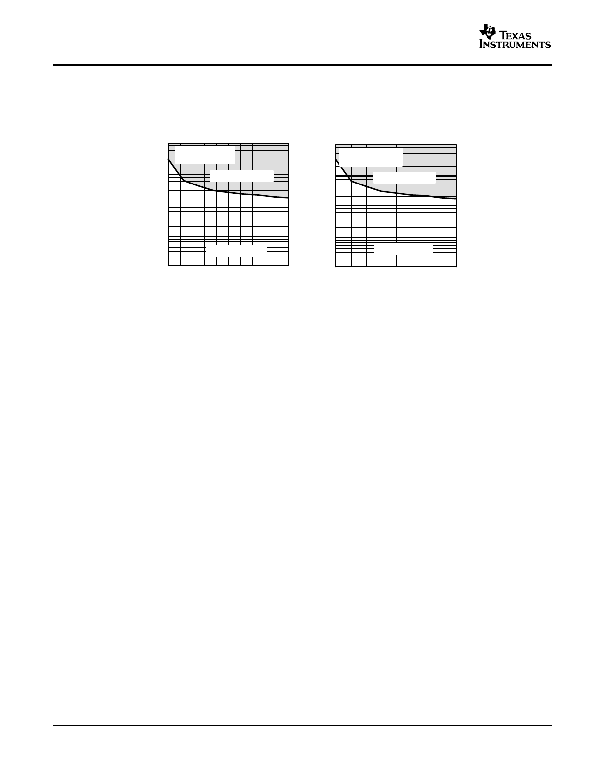
0.01
0.1
1
10
100
I
OUT
(mA)
0 25025 50 75 100 125 150 175 200 225
C
OUT
= 2.2 µF
TA = −40 to 85°C
Region of Instability
Region of Stability
ESR, Equivalent Series Resistance (Ω)
0.01
0.1
1
10
100
1 10 20 40 60 80 120 200 250
I
OUT
(mA)
C
OUT
= 10 µF
TA = −40 to 85°C
Region of Instability
Region of Stability
ESR, Equivalent Series Resistance (Ω)
TPS79401, TPS79418
TPS79425, TPS79428
TPS79430, TPS79433
SLVS349D – NOVEMBER 2001 – REVISED OCTOBER 2004
TYPICAL CHARACTERISTICS (continued)
TPS79428 TYPICAL REGIONS OF TPS79428 TYPICAL REGIONS OF
STABILITY EQUIVALENT SERIES STABILITY EQUIVALENT SERIES
RESISTANCE (ESR) RESISTANCE (ESR)
OUTPUT CURRENT OUTPUT CURRENT
vs vs
Figure 20. Figure 21.
8
Page 9

www.ti.com
TPS794xx
GNDEN NR
IN OUT
V
IN
V
OUT
0.1µF
0.01µF
2.2µF
TPS79401, TPS79418
TPS79425, TPS79428
TPS79430, TPS79433
SLVS349D – NOVEMBER 2001 – REVISED OCTOBER 2004
APPLICATION INFORMATION
The TPS794xx family of low-dropout (LDO) regulators has been optimized for use in noise-sensitive equipment.
The device features extremely low dropout voltages, high PSRR, ultralow output noise, low quiescent current,
and enable input to reduce supply currents to less than 1 µA when the regulator is turned off.
A typical application circuit is shown in Figure 22 .
Figure 22. Typical Application Circuit
External Capacitor Requirements
A 0.1-µF or larger ceramic input bypass capacitor, connected between IN and GND and located close to the
TPS794xx, is required for stability. It improves transient response, noise rejection, and ripple rejection. A
higher-value input capacitor may be necessary if large, fast-rise-time load transients are anticipated or the device
is located several inches from the power source.
Like most low dropout regulators, the TPS794xx requires an output capacitor connected between OUT and GND
to stabilize the internal control loop. The minimum recommended capacitance is 2.2 µF. Any 2.2 µF or larger
ceramic capacitor is suitable.
The internal voltage reference is a key source of noise in an LDO regulator. The TPS794xx has an NR pin which
is connected to the voltage reference through a 250-k Ω internal resistor. The 250-k Ω internal resistor, in
conjunction with an external bypass capacitor connected to the NR pin, creates a low-pass filter to reduce the
voltage reference noise and, therefore, the noise at the regulator output. In order for the regulator to operate
properly, the current flow out of the NR pin must be at a minimum, because any leakage current creates an IR
drop across the internal resistor thus creating an output error. Therefore, the NR capacitor must have minimal
leakage current. The bypass capacitor should be no more than 0.1 µF to ensure that it is fully charged during the
quickstart time provided by the internal switch shown in the functional block diagram.
For example, the TPS79428 exhibits only 32 µV
and a 2.2-µF ceramic output capacitor. Note that the output starts up slower as the bypass capacitance
increases due to the RC time constant at the NR pin that is created by the internal 250-k Ω resistor and external
capacitor.
of output voltage noise using a 0.1-µF ceramic NR capacitor
RMS
9
Page 10
www.ti.com
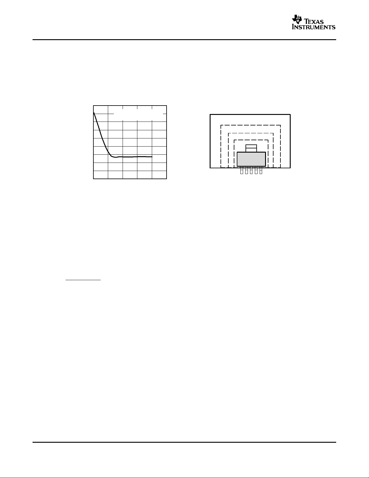
PCB Copper Area − in
100
80
40
0 1 2 3
Thermal Resistance −
120
140
THERMAL RESISTANCE
vs
PCB COPPER AREA
180
4 5
160
60
0
20
JA
θ
C/W
°( )
Surface-Mount Package
1 oz. Copper
CIRCUIT BOARD COPPER AREA
SOT223 Surface-Mount Package
P
D(max)
TJmax T
A
R
θJA
P
D
VIN V
OUT
I
OUT
TPS79401, TPS79418
TPS79425, TPS79428
TPS79430, TPS79433
SLVS349D – NOVEMBER 2001 – REVISED OCTOBER 2004
Board Layout Recommendation to Improve PSRR and Noise Performance
To improve ac measurements like PSRR, output noise, and transient response, it is recommended that the board
be designed with separate ground planes for V
pin of the device. In addition, the ground connection for the bypass capacitor should connect directly to the
ground pin of the device.
and V
IN
, with each ground plane connected only at the ground
OUT
Figure 23. Thermal Resistance vs PCB Area for the SOT223-6.
Power and Dissipation and Junction Temperature
Specified regulator operation is assured to a junction temperature of 125 ° C; the maximum junction temperature
should be restricted to 125 ° C under normal operating conditions. This restriction limits the power dissipation the
regulator can handle in any given application. To ensure the junction temperature is within acceptable limits,
calculate the maximum allowable dissipation, P
equal to P
.
D(max)
The maximum-power-dissipation limit is determined using the following equation:
where:
• TJmax is the maximum allowable junction temperature.
• R θ
is the thermal resistence juntion-to-ambient for the package. See the power dissipation table and
JA
Figure 1
• TAis the ambient temperature.
The regulator dissipation is calculated using:
Power dissipation resulting from quiescent current is negligible. Excessive power dissipation triggers the thermal
protection circuit.
Regulator Mounting
The tab of the SOT223-6 package is electrically connected to ground. For best thermal performance, the tab of
the surface-mount version should be soldered directly to a circuit-board copper area. Increasing the copper area
improves heat dissipation. Solder pad footprint recommendations for the devices are presented in an application
bulletin Solder Pad Recommendations for Surface-Mount Devices, literature number AB-132, available from the
TI web site (www.ti.com).
10
, and the actual dissipation, PD, which must be less than or
D(max)
(1)
(2)
Page 11

www.ti.com
V
OUT
V
REF
1
R1
R2
R1
V
OUT
V
REF
1 R2
C1
(3 x 10⁻⁷) x (R1 R2)
(R1 x R2)
22 pF
15 pF
15 pF
OUTPUT VOLTAGE
PROGRAMMING GUIDE
OUTPUT
VOLTAGE
R1 R2
2.5 V
3.3 V
3.6 V
C1
31.6 kΩ
49.9 kΩ
59 kΩ
30.1 kΩ
30.1 kΩ
30.1 kΩ
†
Not Available on the DCQ package.
TPS794xx
GNDNR FB
IN OUT
EN
V
IN
V
OUT
R1
C1
R2
1µF
2.2µF
0.01µF
TPS79401, TPS79418
TPS79425, TPS79428
TPS79430, TPS79433
SLVS349D – NOVEMBER 2001 – REVISED OCTOBER 2004
Programming the TPS79401 Adjustable LDO Regulator
The output voltage of the TPS79401 adjustable regulator is programmed using an external resistor divider as
shown in Figure 24 . The output voltage is calculated using:
where:
• V
Resistors R1 and R2 should be chosen for approximately 40-µA divider current. Lower value resistors can be
used for improved noise performance, but the device wastes more power. Higher values should be avoided as
leakage current at FB increases the output voltage error. The recommended design procedure is to choose
R2 = 30.1 k Ω to set the divider current at 40 µA, C1 = 15 pF for stability, and then calculate R1 using:
In order to improve the stability of the adjustable version, it is suggested that a small compensation capacitor be
placed between OUT and FB. For voltages < 1.8 V, the value of this capacitor should be 100 pF. For voltages
> 1.8 V, the approximate value of this capacitor can be calculated as:
= 1.2246 V typ (the internal reference voltage).
REF
(3)
(4)
(5)
The suggested value of this capacitor for several resistor ratios is shown in the table below. If this capacitor is
not used (such as in a unity-gain configuration) or if an output voltage < 1.8 V is chosen, then the minimum
recommended output capacitor is 4.7 µF instead of 2.2 µF.
Figure 24. TPS79401 Adjustable LDO Regulator Programming
Regulator Protection
The TPS794xx PMOS-pass transistor has a built-in back diode that conducts reverse current when the input
voltage drops below the output voltage (e.g., during power-down). Current is conducted from the output to the
input and is not internally limited. If extended reverse voltage operation is anticipated, external limiting might be
appropriate.
The TPS794xx features internal current limiting and thermal protection. During normal operation, the TPS794xx
limits output current to approximately 925 mA. When current limiting engages, the output voltage scales back
linearly until the overcurrent condition ends. While current limiting is designed to prevent gross device failure,
care should be taken not to exceed the power dissipation ratings of the package or the absolute maximum
voltage rating of the device. If the temperature of the device exceeds approximately 165 ° C, thermal-protection
circuitry shuts it down. Once the device has cooled down to below approximately 140 ° C, regulator operation
resumes.
11
Page 12

Page 13
Page 14

Page 15

IMPORTANT NOTICE
Texas Instruments Incorporated and its subsidiaries (TI) reserve the right to make corrections, modifications,
enhancements, improvements, and other changes to its products and services at any time and to discontinue
any product or service without notice. Customers should obtain the latest relevant information before placing
orders and should verify that such information is current and complete. All products are sold subject to TI’s terms
and conditions of sale supplied at the time of order acknowledgment.
TI warrants performance of its hardware products to the specifications applicable at the time of sale in
accordance with TI’s standard warranty. Testing and other quality control techniques are used to the extent TI
deems necessary to support this warranty . Except where mandated by government requirements, testing of all
parameters of each product is not necessarily performed.
TI assumes no liability for applications assistance or customer product design. Customers are responsible for
their products and applications using TI components. To minimize the risks associated with customer products
and applications, customers should provide adequate design and operating safeguards.
TI does not warrant or represent that any license, either express or implied, is granted under any TI patent right,
copyright, mask work right, or other TI intellectual property right relating to any combination, machine, or process
in which TI products or services are used. Information published by TI regarding third-party products or services
does not constitute a license from TI to use such products or services or a warranty or endorsement thereof.
Use of such information may require a license from a third party under the patents or other intellectual property
of the third party, or a license from TI under the patents or other intellectual property of TI.
Reproduction of information in TI data books or data sheets is permissible only if reproduction is without
alteration and is accompanied by all associated warranties, conditions, limitations, and notices. Reproduction
of this information with alteration is an unfair and deceptive business practice. TI is not responsible or liable for
such altered documentation.
Resale of TI products or services with statements different from or beyond the parameters stated by TI for that
product or service voids all express and any implied warranties for the associated TI product or service and
is an unfair and deceptive business practice. TI is not responsible or liable for any such statements.
Following are URLs where you can obtain information on other Texas Instruments products and application
solutions:
Products Applications
Amplifiers amplifier.ti.com Audio www.ti.com/audio
Data Converters dataconverter.ti.com Automotive www.ti.com/automotive
DSP dsp.ti.com Broadband www.ti.com/broadband
Interface interface.ti.com Digital Control www.ti.com/digitalcontrol
Logic logic.ti.com Military www.ti.com/military
Power Mgmt power.ti.com Optical Networking www.ti.com/opticalnetwork
Microcontrollers microcontroller.ti.com Security www.ti.com/security
Telephony www.ti.com/telephony
Video & Imaging www.ti.com/video
Wireless www.ti.com/wireless
Mailing Address: Texas Instruments
Post Office Box 655303 Dallas, Texas 75265
Copyright 2004, Texas Instruments Incorporated
 Loading...