

Page 1
SLVS382A – JUNE 2001 – REVISED JULY 2001
150-mA LOW-NOISE LDO WITH IN-RUSH
CURRENT CONTROL FOR USB APPLICATION
TPS78825, TPS78833
FEATURES
150-mA Low-Dropout Regulator
D
D Available in 2.5 V, 3.3 V
D Programmable Slew Rate Control
D Output Noise Typically 56 µV
RMS
D Only 17 µA Quiescent Current at 150 mA
D 1 µA Quiescent Current in Standby Mode
D Dropout Voltage Typically 150 mV at 150 mA
(TPS78833)
D Over Current Limitation
D –40°C to 125°C Operating Junction
Temperature Range
D 5-Pin SOT-23 (DBV) Package
DBV PACKAGE
(TOP VIEW)
GND
EN
1
IN
2
3
OUT
5
4
SR
DESCRIPTION
The TPS78825 and TPS78833 are very small (SOT-23)
package, low-noise LDOs that regulate the output
voltage to 2.5 V and 3.3 V with input voltage ranging
from 2.7 V to an absolute maximum of 13.5 V. These
devices output 150 mA with a peak current of 350 mA
(typ). The TPS788xx family uses the SR pin to program
the output voltage slew rate to control the in-rush
current. This is specifically used in the USB application
where large load capacitance is present at start-up. The
TPS788xx devices use only 17 µA of quiescent current
and exhibit only 56 µV
a 10 µF output capacitor.
The usual PNP pass transistor has been replaced by a
PMOS pass element. Because the PMOS pass element
behaves as a low-value resistor, the dropout voltage is
very low, typically 150 mV at 150 mA of load current, and
is directly proportional to the load current.
The TPS788xx also features a logic-enabled sleep
mode to shut down the regulator, reducing quiescent
current to 1 µA typical at T
of output voltage noise using
RMS
= 25°C.
J
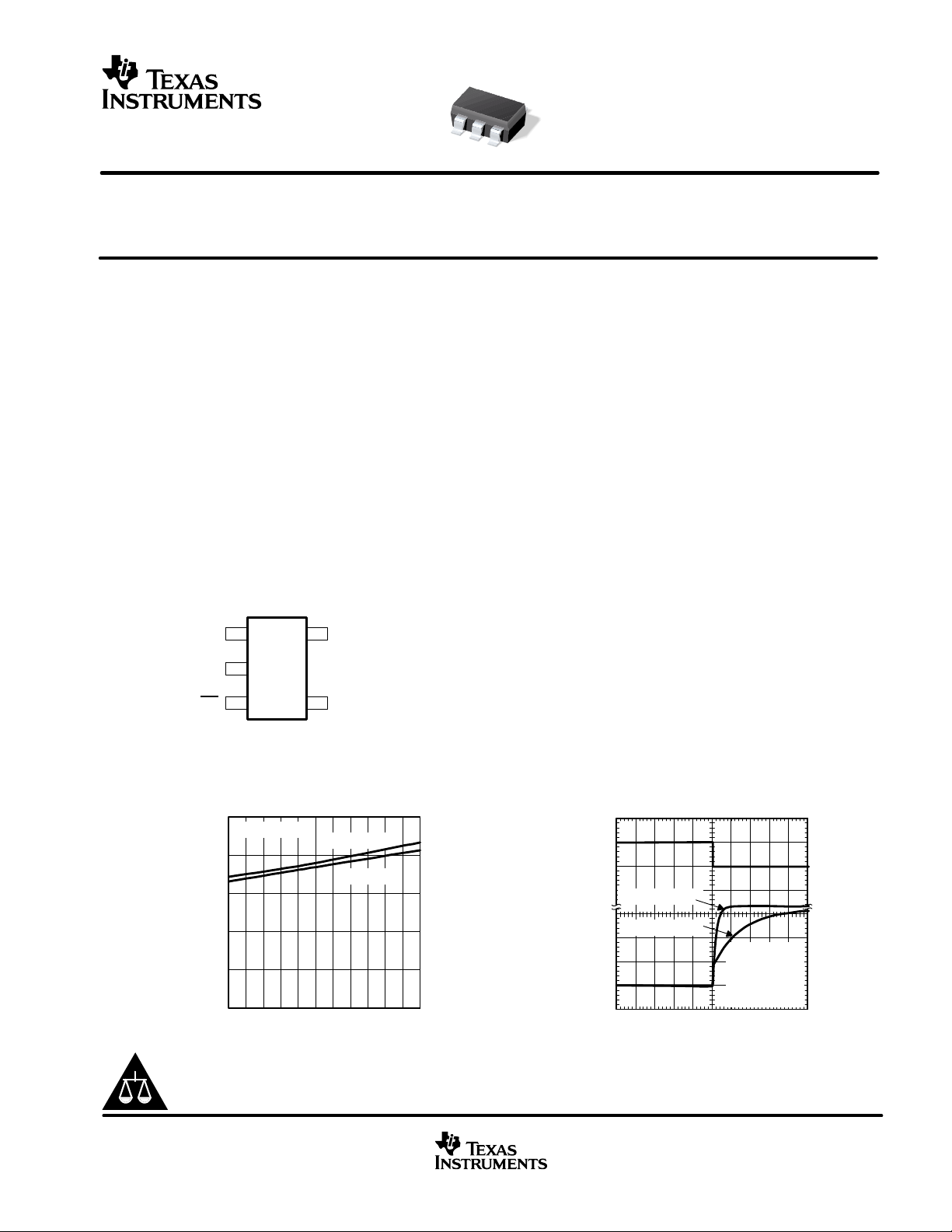
QUIESCENT CURRENT
FREE-AIR TEMPERATURE
25
VCC = 4.3 V
20
Aµ
15
10
Quiescent Current –
5
0
–40–25–10 5 20 35 50 65 80 95 110125
TA – Free-Air Temperature – °C
Please be aware that an important notice concerning availability, standard warranty, and use in critical applications of
Texas Instruments semiconductor products and disclaimers thereto appears at the end of this data sheet.
PRODUCTION DATA information is current as of publication date.
Products conform to specifications per the terms of Texas Instruments
standard warranty. Production processing does not necessarily include
testing of all parameters.
vs
IO = 150 mA
IO = 1 mA
www.ti.com
OUTPUT VOLTAGE, ENABLE VOLTAGE
5
0
Enable Voltage – V
C
= 0.01 µF
(SR)
3
C
(SR)
2
1
0
– Output Voltage – V
O
0302010 40 50 7060 80 90 100
V
Copyright 2001, Texas Instruments Incorporated
vs
TIME (START-UP)
= 0.1 µF
VI = 4.3 V
VO = 3.3 V
IO = 150 mA
Co = 10 µF
TJ = 25°C
t – Time – ms
1
Page 2
TPS78825, TPS78833
SOT 23
SLVS382A – JUNE 2001 – REVISED JULY 2001
T
J
–40°C to 125°C
†
The DBVT indicates tape and reel of 250 parts.
‡
The DBVR indicates tape and reel of 3000 parts.
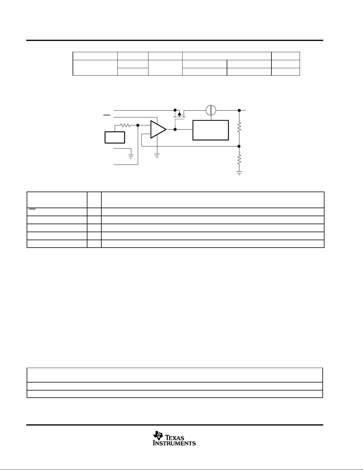
functional block diagram
AVAILABLE OPTIONS
VOLTAGE PACKAGE PART NUMBER SYMBOL
2.5 V
3.3 V
SOT-23
(DBV)
TPS78825DBVT†TPS78825DBVR
TPS78833DBVT TPS78833DBVR PGTI
‡
PGZI
OUT
EN
GND
SR
IN
150 k
V
ref
Current Limit
/ Thermal
Protection
Terminal Functions
TERMINAL
NAME NO.
EN 3 I Active low enable
GND 2 Regulator ground
IN 1 I The IN terminal is the input to the device.
OUT 5 O The OUT terminal is the regulated output of the device.
SR 4 I The SR terminal is used to control the in-rush current.
I/O
DESCRIPTION
absolute maximum ratings over operating free-air temperature range (unless otherwise noted)
Input voltage range –0.3 V to 13.5 V. . . . . . . . . . . . . . . . . . . . . . . . . . . . . . . . . . . . . . . . . . . . . . . . . . . . . . . .
Voltage range at EN –0.3 V to V
Voltage on OUT 7 V. . . . . . . . . . . . . . . . . . . . . . . . . . . . . . . . . . . . . . . . . . . . . . . . . . . . . . . . . . . . . . . . . . . . . . . . . . . . . . . . . .
Peak output current Internally limited. . . . . . . . . . . . . . . . . . . . . . . . . . . . . . . . . . . . . . . . . . . . . . . . . . . . . . . . . . . . . . . . . . . .
ESD rating, HBM 2 kV. . . . . . . . . . . . . . . . . . . . . . . . . . . . . . . . . . . . . . . . . . . . . . . . . . . . . . . . . . . . . . . . . . . . . . . . . . . . . . . .
Continuous total power dissipation See Dissipation Rating Table. . . . . . . . . . . . . . . . . . . . . . . . . . . . . . . . . . . . . . . . . .
Operating virtual junction temperature range, T
Operating ambient temperature range, T
Storage temperature range, T
§
Stresses beyond those listed under “absolute maximum ratings” may cause permanent damage to the device. These are stress ratings only, and
functional operation of the device at these or any other conditions beyond those indicated under “recommended operating conditions” is not
implied. Exposure to absolute-maximum-rated conditions for extended periods may affect device reliability.
NOTE 1: All voltage values are with respect to network ground terminal.
BOARD
Low K
High K
¶
The JEDEC Low K (1s) board design used to derive this data was a 3 inch x 3 inch, two layer board with 2 ounce copper traces on top of the board.
#
The JEDEC High K (2s2p) board design used to derive this data was a 3 inch x 3 inch, multilayer board with 1 ounce internal power and ground
planes and 2 ounce copper traces on top and bottom of the board.
PACKAGE R
¶
DBV 65.8°C/W 259°C/W 3.9 mW/°C 386 mW 212 mW 154 mW
#
DBV 65.8°C/W 180°C/W 5.6 mW/°C 555 mW 305 mW 222 mW
θJC
stg
R
θJA
J
A
DISSIPATION RATING TABLE
DERATING FACTOR
ABOVE TA = 25°C
TA ≤ 25°C
POWER RATING
TA = 70°C
POWER RATING
–40°C to 150°C. . . . . . . . . . . . . . . . . . . . . . . . . . . . . . . . . . . . . . . . . . .
–65°C to 150°C. . . . . . . . . . . . . . . . . . . . . . . . . . . . . . . . . . . . . . . . . . . . . . . . . . . . . . . .
POWER RATING
–40°C to 85°C. . . . . . . . . . . . . . . . . . . . . . . . . . . . . . . . . . . . . . . . . . . . . . . . .
TA = 85°C
+ 0.3 V. . . . . . . . . . . . . . . . . . . . . . . . . . . . . . . . . . . . . . . . . . . . . . . . . . . . . . . . . . . . . . . .
I
§
2
www.ti.com
Page 3
Out ut voltage line regulation (∆VO/VO)
,
R
L
Time, start u (TPS78833)
C
o
µF,
ms
SLVS382A – JUNE 2001 – REVISED JULY 2001
TPS78825, TPS78833
electrical characteristics over recommended operating free-air temperature range EN = 0
TJ = –40 to 125 °C, VI = V
PARAMETER TEST CONDITIONS MIN TYP MAX UNIT
VIInput voltage (see Note 2) 2.7 10 V
I
Continuous output current (see Note 3) 0 150 mA
O
TJOperating junction temperature –40 125 °C
p
Output voltage
Quiescent current (GND current)
Load regulation 10 µA< IO < 200 mA, TJ = 25°C 12 mV
Output voltage line regulation (∆V
(see Note 5)
Output noise voltage (TPS78833)
Time, start-up (TPS78833)
Output current limit
O(typ)
/V
)
+ 1 V , I
TPS78825
TPS78833
= 1 mA, Co = 4.7 µF, C
O
TJ = 25°C 2.5
10 µA< IO < 150 mA, 3.5 V < VI < 10 V 2.425 2.575
TJ = 25°C 3.3
10 µA< IO < 150 mA, 3.8 V < VI < 10 V 3.201 3.399
10 µA< IO < 450 mA, TJ = 25°C 17
10 µA< IO < 150 mA 28
VO + 1 V < VI ≤ 10 V, TJ = 25°C 0.04
VO + 1 V < VI ≤ 10 V 0.1
BW = 200 Hz to 100 kHz,
IO = 150 mA,
TJ = 25°C,
Co = 10 µF,
C
= 0.47 µF
(SR)
R
= 22 Ω
= 22 Ω,
Co = 10 µF,
= 10
TJ = 25°C
VO = 0 V (see Note 4)
C
C
C
= 0.01 µF (unless otherwise noted)
(SR)
56 µV
= 0.01 µF 10
(byp)
= 0.1 µF 50
(byp)
= 0.47 µF 300
(byp)
350 750 mA
,
V
µA
%/V
RMS
ms
Standby current EN = 0 V, 2.7 V < VI < 10 V 1 2 µA
High level enable input voltage 2.7 V < VI < 10 V 1.7 V
Low level enable input voltage 2.7 V < VI < 10 V 0.9 V
Input current (EN) EN = 0 –1 1 µA
f = 1 kHz,
Power supply ripple rejection TPS78833
Dropout voltage (see Note 6) TPS78833
NOTES: 2. To calculate the minimum input voltage for your maximum output current, use the following formula:
VI(min) = VO(max) + VDO (max load)
3. Continuous output current and operating junction temperature are limited by internal protection circuitry , but it is not recommended
that the device operate under conditions beyond those specified in this table for extended periods of time.
4. The minimum IN operating voltage is 2.7 V or V
output current is 200 mA.
5. If VO≤ 2.5 V then V
Line regulation (mV) +ǒ%ńV
If VO > 2.5 V then V
6. IN voltage equals VO(typ) – 100 mV
= 2.7 V, V
Imin
= VO + 1 V, V
Imin
Ǔ
TJ = 25°C,
Co = 10 µF
IO = 150 mA, TJ = 25°C 150
IO = 150 mA 300
+ 1 V , whichever is greater . The maximum IN voltage is 5.5 V . The maximum
O(typ)
= 5.5 V:
Imax
ǒ
V
V
Imax
O
100
= 5.5 V.
Imax
* 2.7 V
Ǔ
1000
C
= 0.01 µF,
(SL)
IO = 150 mA,
70 dB
mV
www.ti.com
3
Page 4

TPS78825, TPS78833
E
E
SLVS382A – JUNE 2001 – REVISED JULY 2001
TYPICAL CHARACTERISTICS
OUTPUT VOLTAGE
vs
LOAD CURRENT
3.315
VCC = 4.3 V
TJ = 25°C
3.31
3.305
3.3
3.295
– Output Voltage – V
O
V
3.29
3.285
0 15 30 45 60 75 90 105 120 135 150
IL – Load Current – mA
Figure 1
OUTPUT SPECTRAL NOISE DENSITY
vs
FREQUENCY
400
Hz
nV/
Output Spectral Noise Density –
300
200
100
0
100
VI = 4.3 V
Co = 4.7 µF
C
= 0.47 µF
(SR)
1 k 10 k 100 k
f – Frequency – Hz
IO = 150 mA
IO = 1 mA
Figure 4
DROPOUT VOLTAGE
vs
FREE-AIR TEMPERATURE
200
VCC = 3.2 V
IO = 150 mA
150
100
– Dropout Voltage – V
50
DO
V
0
–40–25–10 5 20 35 50 65 80 95 110125
TA – Free-Air Temperature – °C
IO = 1 mA
Figure 7
OUTPUT VOLTAGE
vs
FREE-AIR TEMPERATURE
3.2
VCC = 4.3 V
3.315
3.31
3.305
3.3
3.295
3.29
– Output Voltage – V
3.285
O
V
3.28
3.275
3.27
–40 –25 –10 5 20 35 50 65 80 95 110 125
IO = 150 mA
TA – Free-Air Temperature – °C
IO = 1 mA
Figure 2
ROOT MEAN SQUARED OUTPUT NOIS
vs
SLEW RATE CAPACITANCE
100
(RMS)
Vµ
80
60
40
20
0.001 0.01 0.1 1
C
RMS – Root Mean Squared Output Noise –
(sr)
VI = 4.3 V
VO = 3.3 V
IO = 150 mA
Co = 10 µF
BW = 200Hz to 100 kHz
– Slew Rate Capacitance – µF
Figure 5
RIPPLE REJECTION
vs
VI = 4.3 V
VO = 3.3 V
Co = 10 µF
C
= 0.47 µF
(SR)
IO = 150 mA
FREQUENCY
IO = 1 mA
f – Frequency – Hz
Ripple Rejection – dB
120
110
100
90
80
70
60
50
40
30
20
10
Figure 8
QUIESCENT CURRENT
vs
FREE-AIR TEMPERATURE
25
VCC = 4.3 V
20
Aµ
15
10
Quiescent Current –
5
0
–40–25–10 5 20 35 50 65 80 95 110125
TA – Free-Air Temperature – °C
IO = 150 mA
IO = 1 mA
Figure 3
OUTPUT IMPEDANCE
vs
FREQUENCY
2
VI = 4.3 V
1.8
Ω
– Output Impedance –Z
Co = 4.7 µF
1.6
1.4
1.2
1
0.8
0.6
0.4
0.2
IO = 1 mA
IO = 150 mA
0
100 1 M10 1 k
f – Frequency – Hz
10 k
100 k
o
Figure 6
OUTPUT VOLTAGE, ENABLE VOLTAG
vs
TIME (START-UP)
5
0
Enable Voltage – V
3
2
1
0
– Output Voltage – V
O
V
1 M100 k10 k1 k100
0 300200100 400 500 700600 800 900 1000
VI = 4.3 V
VO = 3.3 V
IO = 150 mA
C
= 0.47 µF
(SR)
Co = 10 µF
TJ = 25°C
t – Time – ms
Figure 9
4
www.ti.com
Page 5

TPS78825, TPS78833
SLVS382A – JUNE 2001 – REVISED JULY 2001
TYPICAL CHARACTERISTICS
OUTPUT VOLTAGE, ENABLE VOLTAGE
vs
TIME (START-UP)
5
0
Enable Voltage – V
C
= 0.01 µF
(SR)
3
C
= 0.1 µF
(SR)
2
1
0
– Output Voltage – V
O
0302010 40 50 7060 80 90 100
V
t – Time – ms
VI = 4.3 V
VO = 3.3 V
IO = 150 mA
Co = 10 µF
TJ = 25°C
Figure 10
TYPICAL REGIONS OF STABILITY
EQUIVALENT SERIES RESISTANCE (ESR)
vs
100
10
OUTPUT CURRENT
VI = 4.3 V
VO = 3.3 V
Co = 4.7 µF
Region of Instability
LINE TRANSIENT RESPONSE
VO = 3.3 V
Co = 10 µF
20
– Input Voltage – V
0
I
–20
5.3
4.3
– Output Voltage – mV V
0604020 80 100 140120 160 180 200
O
V
t – Time – µs
dv
dt
Figure 11
LOAD TRANSIENT RESPONSE
0.2 V
=
µs
200
100
0
– Output Current – mA
O
I
50
0
–50
– Change In
O
–100
V
∆
0604020 80 100 140120 160 180
Output Voltage – mV
t – Time – µs
Figure 12
TYPICAL REGIONS OF STABILITY
EQUIVALENT SERIES RESISTANCE (ESR)
vs
100
10
OUTPUT CURRENT
VI = 4.3 V
VO = 3.3 V
Co = 10 µF
Region of Instability
0.075 A
dI
=
dt
VI = 4.3 V
VO = 3.3 V
Co = 10 µF
µs
200
1
Region of Stability
ESR – Equivalent Series Resistance – Ω
0.1
0 60 90 120 150
IO – Output Current – mA
Figure 13
1
Region of Stability
ESR – Equivalent Series Resistance – Ω
0.1
0 60 90 120 150
IO – Output Current – mA
Figure 14
www.ti.com
5
Page 6

TPS78825, TPS78833
SLVS382A – JUNE 2001 – REVISED JULY 2001
APPLICATION INFORMATION
The TPS788xx family of low-dropout (LDO) regulators has been optimized for use in battery-operated
equipment. It features extremely low dropout voltages, low output noise, low quiescent current (17 µA typically),
and enable inputs to reduce supply currents to 1 µA when the regulator is turned off. A typical application circuit
is shown in Figure 15.
1
V
I
1 µF
IN
3
EN
GND
2
SR
OUT
4
5
V
O
+
4.7 µF
ESR = 0.2 Ω
0.01 µF
Figure 15. Typical Application Circuit
external capacitor requirements
Although not required, a 0.047-µF or larger ceramic input bypass capacitor , connected between IN and GND
and located close to the TPS788xx, is recommended to improve transient response and noise rejection. A
higher-value electrolytic input capacitor may be necessary if large, fast-rise-time load transients are anticipated
and the device is located several inches from the power source.
Like all low dropout regulators, the TPS788xx requires an output capacitor connected between OUT and GND
to stabilize the internal control loop. The minimum recommended capacitance is 4.7 µF. The ESR (equivalent
series resistance) of the capacitor should be between 0.2 Ω and 10 Ω. to ensure stability . Capacitor values larger
than 4.7 µF are acceptable, and allow the use of smaller ESR values. Capacitances less than 4.7 µF are not
recommended because they require careful selection of ESR to ensure stability. Solid tantalum electrolytic,
aluminum electrolytic, and multilayer ceramic capacitors are all suitable, provided they meet the requirements
described above. Most of the commercially available 4.7 µF surface-mount solid tantalum capacitors, including
devices from Sprague, Kemet, and Nichico, meet the ESR requirements stated above. Multilayer ceramic
capacitors may have very small equivalent series resistances and may thus require the addition of a low value
series resistor to ensure stability.
CAPACITOR SELECTION
PART NO. MFR. VALUE MAX ESR
T494B475K016AS Kemet 4.7 µF 1.5 Ω 1.9 × 3.5 × 2.8
195D106x0016x2T Sprague 10 µF 1.5 Ω 1.3 × 7.0 × 2.7
695D106x003562T Sprague 10 µF 1.3 Ω 2.5 × 7.6 × 2.5
TPSC475K035R0600 AVX 4.7 µF 0.6 Ω 2.6 × 6.0 × 3.2
†
Size is in mm. The ESR maximum resistance is in Ohms at 100 kHz and TA = 25°C. Contact the
manufacturer for the minimum ESR values.
†
SIZE (H × L × W)
†
6
www.ti.com
Page 7

SLVS382A – JUNE 2001 – REVISED JULY 2001
TPS78825, TPS78833
APPLICATION INFORMATION
external capacitor requirements (continued)
The external bypass capacitor, used in conjunction with an internal resistor to form a low-pass filter, should be
a low ESR ceramic capacitor. For example, the TPS78833 exhibits only 56 µV
a 0.01 µF ceramic bypass capacitor and a 10-µF ceramic output capacitor. Note that the output will start up
slower as the bypass capacitance increases due to the RC time constant at the bypass pin that is created by
the internal 150-kΩ resistor and external capacitor.
of output voltage noise using
RMS
power dissipation and junction temperature
Specified regulator operation is assured to a junction temperature of 125°C; the maximum junction temperature
should be restricted to 125°C under normal operating conditions. This restriction limits the power dissipation
the regulator can handle in any given application. T o ensure the junction temperature is within acceptable limits,
calculate the maximum allowable dissipation, P
or equal to P
The maximum-power-dissipation limit is determined using the following equation:
D(max)
.
, and the actual dissipation, PD, which must be less than
D(max)
P
D(max)
Where:
T
max is the maximum allowable junction temperature.
J
is the thermal resistance junction-to-ambient for the package, see the dissipation rating table.
R
θJA
is the ambient temperature.
T
A
The regulator dissipation is calculated using:
P
+
D
Power dissipation resulting from quiescent current is negligible. Excessive power dissipation will trigger the
thermal protection circuit.
+
ǒ
VI* V
TJmax * T
R
Ǔ
O
θJA
I
A
O
regulator protection
The TPS788xx PMOS-pass transistor has a built-in back diode that conducts reverse current when the input
voltage drops below the output voltage (e.g., during power down). Current is conducted from the output to the
input and is not internally limited. If extended reverse voltage operation is anticipated, external limiting might
be appropriate.
The TPS788xx features internal current limiting and thermal protection. During normal operation, the TPS78833
limits output current to approximately 350 mA. When current limiting engages, the output voltage scales back
linearly until the overcurrent condition ends. While current limiting is designed to prevent gross device failure,
care should be taken not to exceed the power dissipation ratings of the package. If the temperature of the device
exceeds approximately 165°C, thermal-protection circuitry shuts it down. Once the device has cooled down to
below approximately 140°C, regulator operation resumes.
www.ti.com
7
Page 8

IMPORTANT NOTICE
Texas Instruments Incorporated and its subsidiaries (TI) reserve the right to make corrections, modifications, enhancements, improvements,
and other changes to its products and services at any time and to discontinue any product or service without notice. Customers should
obtain the latest relevant information before placing orders and should verify that such information is current and complete. All products are
sold subject to TI’s terms and conditions of sale supplied at the time of order acknowledgment.
TI warrants performance of its hardware products to the specifications applicable at the time of sale in accordance with TI’s standard
warranty. Testing and other quality control techniques are used to the extent TI deems necessary to support this warranty. Except where
mandated by government requirements, testing of all parameters of each product is not necessarily performed.
TI assumes no liability for applications assistance or customer product design. Customers are responsible for their products and
applications using TI components. To minimize the risks associated with customer products and applications, customers should provide
adequate design and operating safeguards.
TI does not warrant or represent that any license, either express or implied, is granted under any TI patent right, copyright, mask work right,
or other TI intellectual property right relating to any combination, machine, or process in which TI products or services are used. Information
published by TI regarding third-party products or services does not constitute a license from TI to use such products or services or a
warranty or endorsement thereof. Use of such information may require a license from a third party under the patents or other intellectual
property of the third party, or a license from TI under the patents or other intellectual property of TI.
Reproduction of TI information in TI data books or data sheets is permissible only if reproduction is without alteration and is accompanied
by all associated warranties, conditions, limitations, and notices. Reproduction of this information with alteration is an unfair and deceptive
business practice. TI is not responsible or liable for such altered documentation. Information of third parties may be subject to additional
restrictions.
Resale of TI products or services with statements different from or beyond the parameters stated by TI for that product or service voids all
express and any implied warranties for the associated TI product or service and is an unfair and deceptive business practice. TI is not
responsible or liable for any such statements.
TI products are not authorized for use in safety-critical applications (such as life support) where a failure of the TI product would reasonably
be expected to cause severe personal injury or death, unless officers of the parties have executed an agreement specifically governing
such use. Buyers represent that they have all necessary expertise in the safety and regulatory ramifications of their applications, and
acknowledge and agree that they are solely responsible for all legal, regulatory and safety-related requirements concerning their products
and any use of TI products in such safety-critical applications, notwithstanding any applications-related information or support that may be
provided by TI. Further, Buyers must fully indemnify TI and its representatives against any damages arising out of the use of TI products in
such safety-critical applications.
TI products are neither designed nor intended for use in military/aerospace applications or environments unless the TI products are
specifically designated by TI as military-grade or "enhanced plastic." Only products designated by TI as military-grade meet military
specifications. Buyers acknowledge and agree that any such use of TI products which TI has not designated as military-grade is solely at
the Buyer's risk, and that they are solely responsible for compliance with all legal and regulatory requirements in connection with such use.
TI products are neither designed nor intended for use in automotive applications or environments unless the specific TI products are
designated by TI as compliant with ISO/TS 16949 requirements. Buyers acknowledge and agree that, if they use any non-designated
products in automotive applications, TI will not be responsible for any failure to meet such requirements.
Following are URLs where you can obtain information on other Texas Instruments products and application solutions:
Products Applications
Amplifiers amplifier.ti.com Audio www.ti.com/audio
Data Converters dataconverter.ti.com Automotive www.ti.com/automotive
DLP® Products www.dlp.com Communications and www.ti.com/communications
DSP dsp.ti.com Computers and www.ti.com/computers
Clocks and Timers www.ti.com/clocks Consumer Electronics www.ti.com/consumer-apps
Interface interface.ti.com Energy www.ti.com/energy
Logic logic.ti.com Industrial www.ti.com/industrial
Power Mgmt power.ti.com Medical www.ti.com/medical
Microcontrollers microcontroller.ti.com Security www.ti.com/security
RFID www.ti-rfid.com Space, Avionics & www.ti.com/space-avionics-defense
RF/IF and ZigBee® Solutions www.ti.com/lprf Video and Imaging www.ti.com/video
Mailing Address: Texas Instruments, Post Office Box 655303, Dallas, Texas 75265
Copyright © 2010, Texas Instruments Incorporated
Telecom
Peripherals
Defense
Wireless www.ti.com/wireless-apps
Page 9

 Loading...