

Page 1
查询TPS75501KTT供应商
TPS75515, TPS75518, TPS75525, TPS75533 WITH POWER GOOD AND
TPS75501 FAST-TRANSIENT RESPONSE 5-A LOW-DROPOUT
VOLTAGE REGULATORS
SLVS293D – NOVEMBER 2000 – REVISED MAY 2002
D 5-A Low-Dropout Voltage Regulator
D Available in 1.5-V, 1.8-V, 2.5-V, and 3.3-V
Fixed-Output and Adjustable Versions
D Open Drain Power-Good (PG) Status
Output (Fixed Options Only)
D Dropout Voltage Typically 250 mV at 5 A
(TPS75533)
D Low 125 µA Typical Quiescent Current
D Fast Transient Response
D 3% Tolerance Over Specified Conditions for
Fixed-Output Versions
D Available in 5-Pin TO–220 and TO–263
Surface-Mount Packages
D Thermal Shutdown Protection
EN
IN
GND
OUTPUT
FB/PG
GND
OUTPUT
FB/PG
TO–220 (KC) PACKAGE
(TOP VIEW)
1
2
3
4
5
TO–263 (KTT) PACKAGE
(TOP VIEW)
EN
IN
1
2
3
4
5
Tab is GND
description
The TPS755xx family of 5-A low dropout (LDO) regulators contains four fixed voltage option regulators with
integrated power-good (PG
5 A of output current with a dropout of 250 mV (TPS75533). Therefore, the device is capable of performing a
3.3-V to 2.5-V conversion. Quiescent current is 125 µA at full load and drops down to less than 1 µA when the
device is disabled. The TPS755xx is designed to have fast transient response for large load current changes.
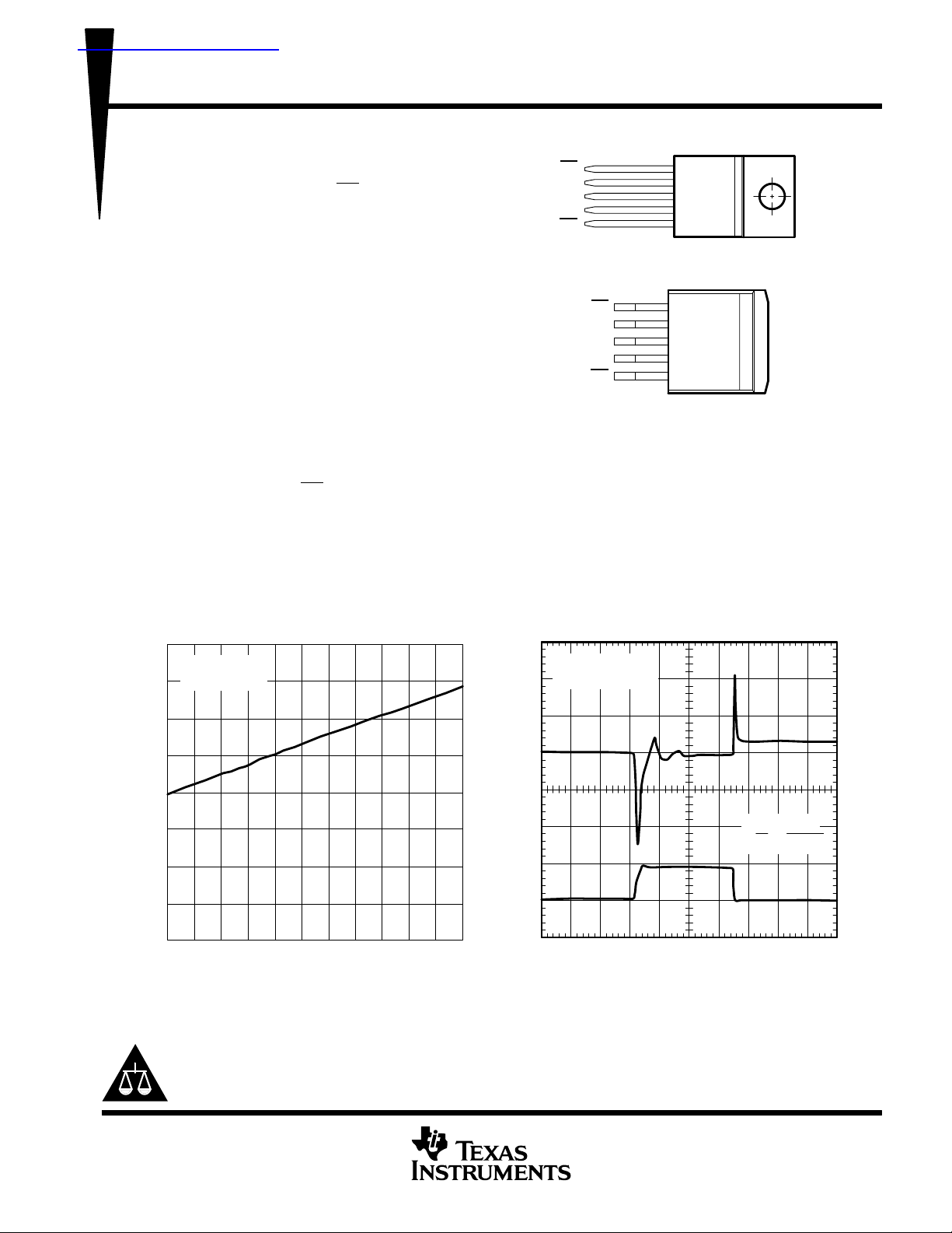
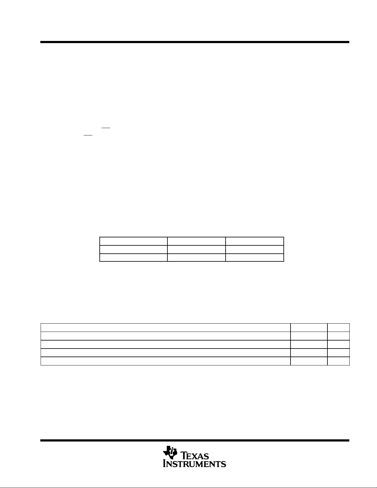
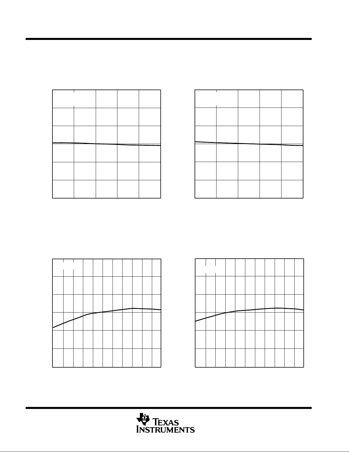
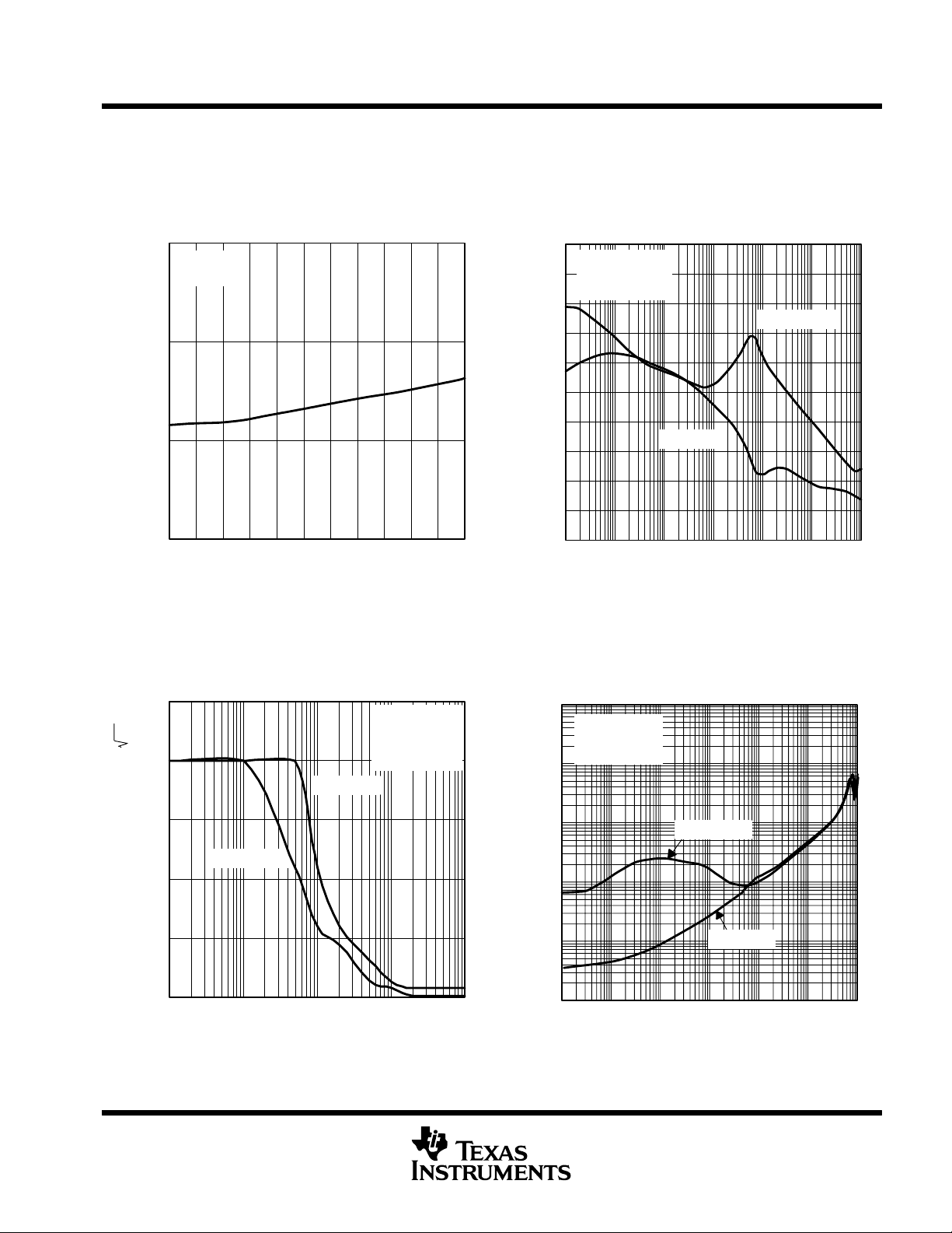
DROPOUT VOLTAGE
JUNCTION TEMPERATURE
400
IO = 5 A
VO = 3.3 V
350
) and an adjustable voltage option regulator. These devices are capable of supplying
TPS75533
vs
150
100
LOAD TRANSIENT RESPONSE
VO = 1.5 V
Co = 100 µF
TPS75515
Tab is GND
300
250
200
150
– Dropout Voltage – mV
DO
V
100
50
0
–40 –25 –10 5 20 35 50 65 80 95 110 125
TJ – Junction Temperature – °C
Please be aware that an important notice concerning availability, standard warranty, and use in critical applications of
Texas Instruments semiconductor products and disclaimers thereto appears at the end of this data sheet.
PRODUCTION DATA information is current as of publication date.
Products conform to specifications per the terms of Texas Instruments
standard warranty. Production processing does not necessarily include
testing of all parameters.
50
0
–50
–100
– Change in Output Voltage – mV
O
V
∆
–150
0604020 80 100 140120 160 180 200
t – Time – µs
Copyright 2001, Texas Instruments Incorporated
di
dt
+
1.25 A
µs
5
0
O
I – Output Current – A
POST OFFICE BOX 655303 • DALLAS, TEXAS 75265
1
Page 2
TPS75515, TPS75518, TPS75525, TPS75533 WITH POWER GOOD AND
TPS75501 FAST-TRANSIENT RESPONSE 5-A LOW-DROPOUT
VOLTAGE REGULATORS
SLVS293D – NOVEMBER 2000 – REVISED MAY 2002
description (continued)
Because the PMOS device behaves as a low-value resistor, the dropout voltage is very low (typically 250 mV
at an output current of 5 A for the TPS75533) and is directly proportional to the output current. Additionally , since
the PMOS pass element is a voltage-driven device, the quiescent current is very low and independent of output
loading (typically 125 µA over the full range of output current). These two key specifications yield a significant
improvement in operating life for battery-powered systems.
The device is enabled when EN
applying a TTL high signal to EN
1 µA at T
= 25°C. The power-good terminal (PG) is an active low, open drain output, which can be used to
J
is connected to a low-level voltage. This LDO family also features a sleep mode;
(enable) shuts down the regulator, reducing the quiescent current to less than
implement a power-on reset or a low-battery indicator.
The TPS755xx is offered in 1.5-V, 1.8-V, 2.5-V , and 3.3-V fixed-voltage versions and in an adjustable version
(programmable over the range of 1.22 V to 5 V). Output voltage tolerance is specified as a maximum of 3% over
line, load, and temperature ranges. The TPS755xx family is available in a 5-pin TO–220 (KC) and TO–263 (KTT)
packages.
AVAILABLE OPTIONS
T
J
–40°C to 125°C
NOTE: The TPS75501 is programmable using an external resistor divider (see application
information). The KTT package is available taped and reeled. Add an R suffix to the
device type (e.g., TPS75501KTTR) to indicate tape and reel.
OUTPUT VOLTAGE
(TYP)
3.3 V TPS75533KC TPS75533KTT
2.5 V TPS75525KC TPS75525KTT
1.8 V TPS75518KC TPS75518KTT
1.5 V TPS75515KC TPS75515KTT
Adjustable 1.22 V to 5 V TPS75501KC TPS75501KTT
2
V
I
IN
TO–220 (KC) TO–263(KTT)
PG
5
PG
4
OUT
1 µF
†
See application information section for capacitor selection details.
1
EN
GND
3
+
C
47 µF
V
O
†
o
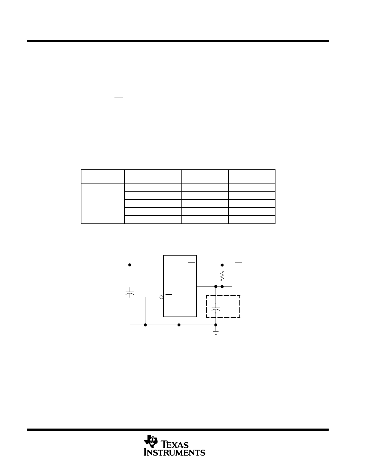
Figure 1. Typical Application Configuration (For Fixed Output Options)
2
POST OFFICE BOX 655303 • DALLAS, TEXAS 75265
Page 3
TPS75515, TPS75518, TPS75525, TPS75533 WITH POWER GOOD AND
TPS75501 FAST-TRANSIENT RESPONSE 5-A LOW-DROPOUT
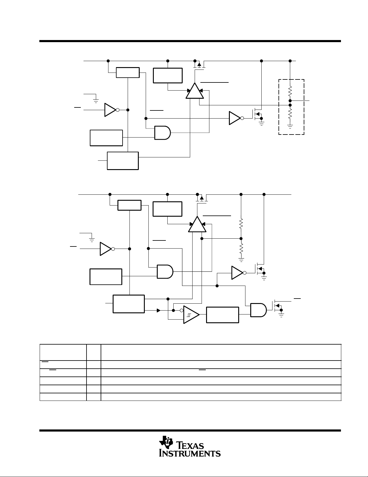
functional block diagram—adjustable version
SLVS293D – NOVEMBER 2000 – REVISED MAY 2002
VOLTAGE REGULATORS
V
IN
V
ref
Current
UVLO
= 1.22 V
GND
EN
Thermal
Shutdown
V
IN
UVLO
Bandgap
Reference
functional block diagram—fixed version
V
IN
UVLO
GND
EN
Current
UVLO
Sense
Sense
ILIM
ILIM
SHUTDOWN
_
+
_
+
SHUTDOWN
R1
R2
R1
R2
External to
the Device
V
OUT
V
OUT
FB
Thermal
Shutdown
V
= 1.22 V
V
IN
Bandgap
Reference
ref
Falling
Edge Delay
Terminal Functions (TPS755xx)
TERMINAL
NAME NO.
EN 1 I Enable input
FB/PG 5 I Feedback input voltage for adjustable device/PG output for fixed options
GND 3 Regulator ground
IN 2 I Input voltage
OUTPUT 4 O Regulated output voltage
I/O
DESCRIPTION
PG
POST OFFICE BOX 655303 • DALLAS, TEXAS 75265
3
Page 4
TPS75515, TPS75518, TPS75525, TPS75533 WITH POWER GOOD AND
TPS75501 FAST-TRANSIENT RESPONSE 5-A LOW-DROPOUT
VOLTAGE REGULATORS
SLVS293D – NOVEMBER 2000 – REVISED MAY 2002
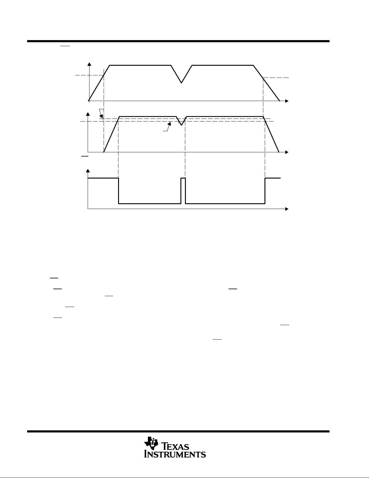
TPS755xx PG timing diagram
V
IN1
V
UVLO
V
UVLO
t
V
OUT
Threshold
Voltage
PG
Output
NOTE A: VIT –Trip voltage is typically 9% lower than the output voltage (91%VO). V
V
(see Note A)
IT+
V
(see Note A)
IT–
IT–
to V
is the hysteresis voltage.
IT+
t
t
detailed description
The TPS755xx family includes four fixed-output voltage regulators (1.5 V, 1.8 V, 2.5 V, and 3.3 V), and an
adjustable regulator, the TPS75501 (adjustable from 1.22 V to 5 V). The bandgap voltage is typically 1.22 V.
pin functions
enable (EN)
The EN
shutdown mode. When EN
power-good (PG
The PG
of V
impedance state. It will go to a high-impedance state when V
condition) of the regulated voltage. The open drain output of the PG
terminal is an input which enables or shuts down the device. If EN is a logic high, the device will be in
goes to logic low, the device will be enabled.
)
terminal for the fixed voltage option devices is an open drain, active low output that indicates the status
(output of the LDO). When V
O
reaches approximately 91% of the regulated voltage, PG will go to a low
O
falls below approximately 89% (i.e. over load
O
terminal requires a pullup resistor.
feedback (FB)
FB is an input terminal used for the adjustable-output option and must be connected to the output terminal either
directly, in order to generate the minimum output voltage of 1.22 V, or through an external feedback resistor
divider for other output voltages. The FB connection should be as short as possible. It is essential to route it in
such a way to minimize/avoid noise pickup. Adding RC networks between FB terminal and V
to filter noise is
O
not recommended because it may cause the regulator to oscillate.
4
POST OFFICE BOX 655303 • DALLAS, TEXAS 75265
Page 5
TPS75515, TPS75518, TPS75525, TPS75533 WITH POWER GOOD AND
detailed description (continued)
input voltage (IN)
TPS75501 FAST-TRANSIENT RESPONSE 5-A LOW-DROPOUT
VOLTAGE REGULATORS
SLVS293D – NOVEMBER 2000 – REVISED MAY 2002
The V
terminal is an input to the regulator.
IN
output voltage (OUTPUT)
The V
OUTPUT
terminal is an output to the regulator.
absolute maximum ratings over operating junction temperature range (unless otherwise noted)
‡
Input voltage range
Voltage range at EN
Maximum PG
voltage (fixed options only) 6 V. . . . . . . . . . . . . . . . . . . . . . . . . . . . . . . . . . . . . . . . . . . . . . . . . . . . . .
Peak output current Internally limited. . . . . . . . . . . . . . . . . . . . . . . . . . . . . . . . . . . . . . . . . . . . . . . . . . . . . . . . . . . . . .
Continuous total power dissipation See Dissipation Rating Tables. . . . . . . . . . . . . . . . . . . . . . . . . . . . . . . . . . . .
Output voltage, V
Operating junction temperature range, T
Storage temperature range, T
ESD rating, HBM 2 kV. . . . . . . . . . . . . . . . . . . . . . . . . . . . . . . . . . . . . . . . . . . . . . . . . . . . . . . . . . . . . . . . . . . . . . . . . .
ESD rating, CDM 500 V. . . . . . . . . . . . . . . . . . . . . . . . . . . . . . . . . . . . . . . . . . . . . . . . . . . . . . . . . . . . . . . . . . . . . . . . .
†
Stresses beyond those listed under “absolute maximum ratings” may cause permanent damage to the device. These are stress ratings only, and
functional operation of the device at these or any other conditions beyond those indicated under “recommended operating conditions” is not
implied. Exposure to absolute-maximum-rated conditions for extended periods may affect device reliability.
‡
All voltage values are with respect to network terminal ground.
, VI –0.3 V to 6 V. . . . . . . . . . . . . . . . . . . . . . . . . . . . . . . . . . . . . . . . . . . . . . . . . . . . . . . . . . . . .
–0.3 V to 6 V. . . . . . . . . . . . . . . . . . . . . . . . . . . . . . . . . . . . . . . . . . . . . . . . . . . . . . . . . . . . . . . .
(OUTPUT, FB) 5.5 V. . . . . . . . . . . . . . . . . . . . . . . . . . . . . . . . . . . . . . . . . . . . . . . . . . . . . . . . . .
O
–65°C to 150°C. . . . . . . . . . . . . . . . . . . . . . . . . . . . . . . . . . . . . . . . . . . . . . . . . . .
stg
PACKAGE
TO–220 2 58.7
TO–263 2 38.7
§
For both packages, the R
with 1 ounce internal copper plane and ground plane. There was no air flow across the
packages.
¶
R
was computed assuming a vertical, free standing TO-220 package with pins
θJA
soldered to the board. There is no heatsink attached to the package.
#
R
was computed assuming a horizontally mounted TO-263 package with pins
θJA
soldered to the board. There is no copper pad underneath the package.
–40°C to 150°C. . . . . . . . . . . . . . . . . . . . . . . . . . . . . . . . . . . . . . . . . . .
J
DISSIPATION RATING TABLE
R
(°C/W) R
θJC
values were computed using JEDEC high K board (2S2P)
θJA
θJA
(°C/W)
¶
#
§
Ĕ
recommended operating conditions
Input voltage, V
Output voltage range, V
Output current, I
Operating virtual junction temperature, T
||
To calculate the minimum input voltage for your maximum output current, use the following equation: V
||
I
O
O
J
POST OFFICE BOX 655303 • DALLAS, TEXAS 75265
I(min)
MIN MAX UNIT
2.8 5.5 V
1.22 5 V
0 5 A
–40 125
= V
O(max)
+ V
DO(max load)
°C
.
5
Page 6
TPS75515, TPS75518, TPS75525, TPS75533 WITH POWER GOOD AND
Adj
V
TPS75501 FAST-TRANSIENT RESPONSE 5-A LOW-DROPOUT
VOLTAGE REGULATORS
SLVS293D – NOVEMBER 2000 – REVISED MAY 2002
electrical characteristics over recommended operating junction temperature range (TJ = –40°C to
125°C), V
Output voltage (see Note 2)
Quiescent current (GND current) (see Notes 2 and 3)
Output voltage line regulation (∆VO/VO) (see Note 3)
Load regulation (see Note 2) 0.35 %/V
Output noise voltage TPS75515 BW = 300 Hz to 50 kHz, TJ = 25°C, VI = 2.8 V 35 µVrms
Output current limit VO = 0 V 5.5 10 14 A
Thermal shutdown junction temperature 150 °C
Standby current
FB input current TPS75501 FB = 1.5 V –1 1 µA
Power supply ripple rejection TPS75515
Minimum input voltage for valid PG I
PG trip threshold voltage Fixed options only VO decreasing 89 93 %V
PG hysteresis voltage Fixed options only Measured at V
PG output low voltage Fixed options only VI = 2.8 V, I
PG leakage current Fixed options only V
NOTES: 1. The adjustable option operates with a 2% tolerance over TJ = 0 to 125 °C.
= V
I
O(typ)
2. IO = 1 mA to 5 A
3. If V
≤ 2.5 V then V
O
+ 1 V, IO = 1 mA, EN = 0 V, CO = 100 µF (unless otherwise noted)
PARAMETER TEST CONDITIONS MIN TYP MAX UNIT
1.22 V ≤ VO ≤ 5.5 V, TJ = 25°C V
ustable voltage
1.5 V Output
1.8 V Output
2.5 V Output
3.3 V Output
= 2.8 V, V
Imin
Imax
1.22 V ≤ VO ≤ 5.5 V 0.97 V
1.22 V ≤ VO ≤ 5.5 V, TJ = 0 to 125°C
(see Note 1)
TJ = 25°C, 2.8 V < VI < 5.5 V 1.5
2.8 V ≤ VI ≤ 5.5 V 1.455 1.545
TJ = 25°C, 2.8 V < VI < 5.5 V 1.8
2.8 V ≤ VI ≤ 5.5 V 1.746 1.854
TJ = 25°C, 3.5 V < VI < 5.5 V 2.5
3.5 V ≤ VI ≤ 5.5 V 2.425 2.575
TJ = 25°C, 4.3 V < VI < 5.5 V 3.3
4.3 V ≤ VI ≤ 5.5 V 3.201 3.399
TJ = 25°C 125
VO + 1 V ≤ VI ≤ 5.5 V, TJ = 25°C 0.04
VO + 1 V ≤ VI < 5.5 V 0.1
EN = VI,T
EN = V
I
f = 100 Hz, TJ = 25°C,
VI = 2.8 V, IO = 5 A
= 300 µA, V
O(PG)
= 5 V 1 µA
(PG)
= 5.5 V:
Line regulation (mV) +ǒ%ńV
0.98 V
= 25°C 0.1 µA
J
≤ 0.8 V 0 V
(PG)
O
= 1 mA 0.15 0.4 V
O(PG)
ǒ
V
V
* 2.8 V
Imax
O
Ǔ
100
Ǔ
1000
O
O
O
60 dB
0.5 %V
1.03 V
1.02 V
O
O
200
10 µA
µA
%/V
V
V
V
O
O
If VO > 2.5 V then V
6
= VO + 1 V, V
Imin
Imax
= 5.5 V:
Line regulation (mV) +ǒ%ńV
POST OFFICE BOX 655303 • DALLAS, TEXAS 75265
ǒ
V
V
Imax
O
Ǔ
ǒ
*
VO) 1V
100
Ǔ
Ǔ
1000
Page 7
TPS75515, TPS75518, TPS75525, TPS75533 WITH POWER GOOD AND
V
O
TPS75501 FAST-TRANSIENT RESPONSE 5-A LOW-DROPOUT
VOLTAGE REGULATORS
SLVS293D – NOVEMBER 2000 – REVISED MAY 2002
electrical characteristics over recommended operating junction temperature range (TJ = –40°C to
125°C), V
Input current (EN)
High level EN input voltage 2 V
Low level EN input voltage 0.7 V
V
O
V
I
NOTE 4: IN voltage equals VO(typ) – 100 mV; TPS75515, TPS75518, and TPS75525 dropout voltage limited by input voltage range limitations
= V
I
O(typ)
Dropout voltage, (3.3 V output) (see Note 4)
Discharge transistor current VO = 1.5 V, TJ = 25°C 10 25 mA
UVLO TJ = 25°C, VI rising 2.2 2.75 V
UVLO hysteresis TJ = 25°C, VI falling 100 mV
(i.e., TPS75533 input voltage is set to 3.2 V for the purpose of this test).
+ 1 V, IO = 1 mA, EN = 0 V, CO = 100 µF (unless otherwise noted) (continued)
PARAMETER TEST CONDITIONS
EN = V
I
EN = 0 V –1 0 1 µA
IO = 5 A, VI = 3.2 V, TJ = 25°C 250
IO = 5 A, VI = 3.2 V 500
MIN TYP MAX UNIT
–1 1 µA
TYPICAL CHARACTERISTICS
mV
Table of Graphs
FIGURE
V
O
z
o
V
DO
V
I
V
O
Output voltage
Ground current vs Junction temperature 6
Power supply ripple rejection vs Frequency 7
Output spectral noise density vs Frequency 8
Output impedance vs Frequency 9
Dropout voltage
Minimum required input voltage vs Output voltage 12
Line transient response 13, 15
Load transient response 14, 16
Output voltage and enable voltage vs Time (start-up) 17
Equivalent series resistance vs Output current 19, 20
vs Output current 2, 3
vs Junction temperature
vs Input voltage 10
vs Junction temperature
4, 5
11
POST OFFICE BOX 655303 • DALLAS, TEXAS 75265
7
Page 8
TPS75515, TPS75518, TPS75525, TPS75533 WITH POWER GOOD AND
TPS75501 FAST-TRANSIENT RESPONSE 5-A LOW-DROPOUT
VOLTAGE REGULATORS
SLVS293D – NOVEMBER 2000 – REVISED MAY 2002
TYPICAL CHARACTERISTICS
– Output Voltage – V
O
V
3.345
3.330
3.315
3.3
3.285
3.270
3.255
VI = 4.3 V
TJ = 25°C
0
TPS75533
OUTPUT VOLTAGE
TPS75515
OUTPUT VOLTAGE
vs
OUTPUT CURRENT
1.545
1.530
1.515
1.485
– Output Voltage – V
O
V
1.470
15
24
IO – Output Current – A
3
1.455
VI = 2.8 V
TJ = 25°C
1.5
0
Figure 2
OUTPUT CURRENT
152
IO – Output Current – A
Figure 3
vs
34
TPS75533
OUTPUT VOLTAGE
vs
JUNCTION TEMPERATURE
3.345
VI = 4.3 V
3.33
3.315
3.3
3.285
– Output Voltage – V
O
V
3.270
3.255
–40 –25 10 35 50 65 11095
5 125
20 80
TJ – Junction Temperature – °C
Figure 4
TPS75515
OUTPUT VOLTAGE
vs
JUNCTION TEMPERATURE
1.545
VI = 2.8 V
1.530
1.515
1.5
1.485
– Output Voltage – V
O
V
1.470
1.455
–40 20 11035 95–25 –10 5 50 65 80 125
TJ – Junction Temperature – °C
Figure 5
8
POST OFFICE BOX 655303 • DALLAS, TEXAS 75265
Page 9
TPS75515, TPS75518, TPS75525, TPS75533 WITH POWER GOOD AND
TPS75501 FAST-TRANSIENT RESPONSE 5-A LOW-DROPOUT
VOLTAGE REGULATORS
SLVS293D – NOVEMBER 2000 – REVISED MAY 2002
TYPICAL CHARACTERISTICS
TPS755xx
GROUND CURRENT
vs
JUNCTION TEMPERATURE
150
VI = 5 V
IO = 5 A
125
100
Ground Current – Aµ
75
–40 –25 –10 5 20 35 50 65 80 95 110 125
TJ – Junction Temperature – °C
Figure 6
PSRR – Power Supply Ripple Rejection – dB
TPS75733
POWER SUPPLY RIPPLE REJECTION
vs
FREQUENCY
90
VI = 4.3 V
80
Co = 100 µF
TJ = 25°C
70
60
50
40
30
20
10
0
IO = 5 A
1k10010
f – Frequency – Hz
100k10k
Figure 7
IO = 1 mA
1M
10M
TPS75533
OUTPUT SPECTRAL NOISE DENSITY
vs
FREQUENCY
2.5
V/ HzOutput Spectral Noise Density – µ
2
IO = 5 A
1.5
IO = 1 mA
1
0.5
0
1010 100 1k 10k 100k
f – Frequency – Hz
VI = 4.3 V
VO = 3.3 V
Co = 100 µF
TJ = 25°C
Figure 8
TPS75533
OUTPUT IMPEDANCE
vs
FREQUENCY
100
VI = 4.3 V
Co = 100 µF
TJ = 25°C
10
Ω
1
0.1
– Output Impedance –z
o
0.01
0.001
10 100 100k 1M
IO = 1 mA
10k1k 10M
f – Frequency – Hz
Figure 9
IO = 5 A
POST OFFICE BOX 655303 • DALLAS, TEXAS 75265
9
Page 10

TPS75515, TPS75518, TPS75525, TPS75533 WITH POWER GOOD AND
TPS75501 FAST-TRANSIENT RESPONSE 5-A LOW-DROPOUT
VOLTAGE REGULATORS
SLVS293D – NOVEMBER 2000 – REVISED MAY 2002
TYPICAL CHARACTERISTICS
TPS75501
DROPOUT VOLTAGE
vs
INPUT VOLTAGE
450
IO = 5 A
TJ = 125°C
TJ = 25°C
TJ = –40°C
50
0
2.5 3 3.5 4 4.5 5
VI – Input Voltage – V
– Dropout Voltage – mV
DO
V
400
350
300
250
200
150
100
Figure 10
TPS75533
DROPOUT VOLTAGE
vs
JUNCTION TEMPERATURE
400
IO = 5 A
VO = 3.3 V
350
300
250
200
150
– Dropout Voltage – mV
DO
V
100
50
0
–40 –25 –10 5 20 35 50 65 80 95 110 125
TJ – Junction Temperature – °C
Figure 11
MINIMUM REQUIRED INPUT VOLTAGE
vs
OUTPUT VOLTAGE
4
IO = 5 A
TJ = 125°C
TJ = 25°C
TJ = –40°C
3
2.8
– Minimum Required Input Voltage – V
I
V
2
1.5 2.5 3.523
1.75 2.25 2.75 3.25
VO – Output Voltage – V
Figure 12
TPS75515
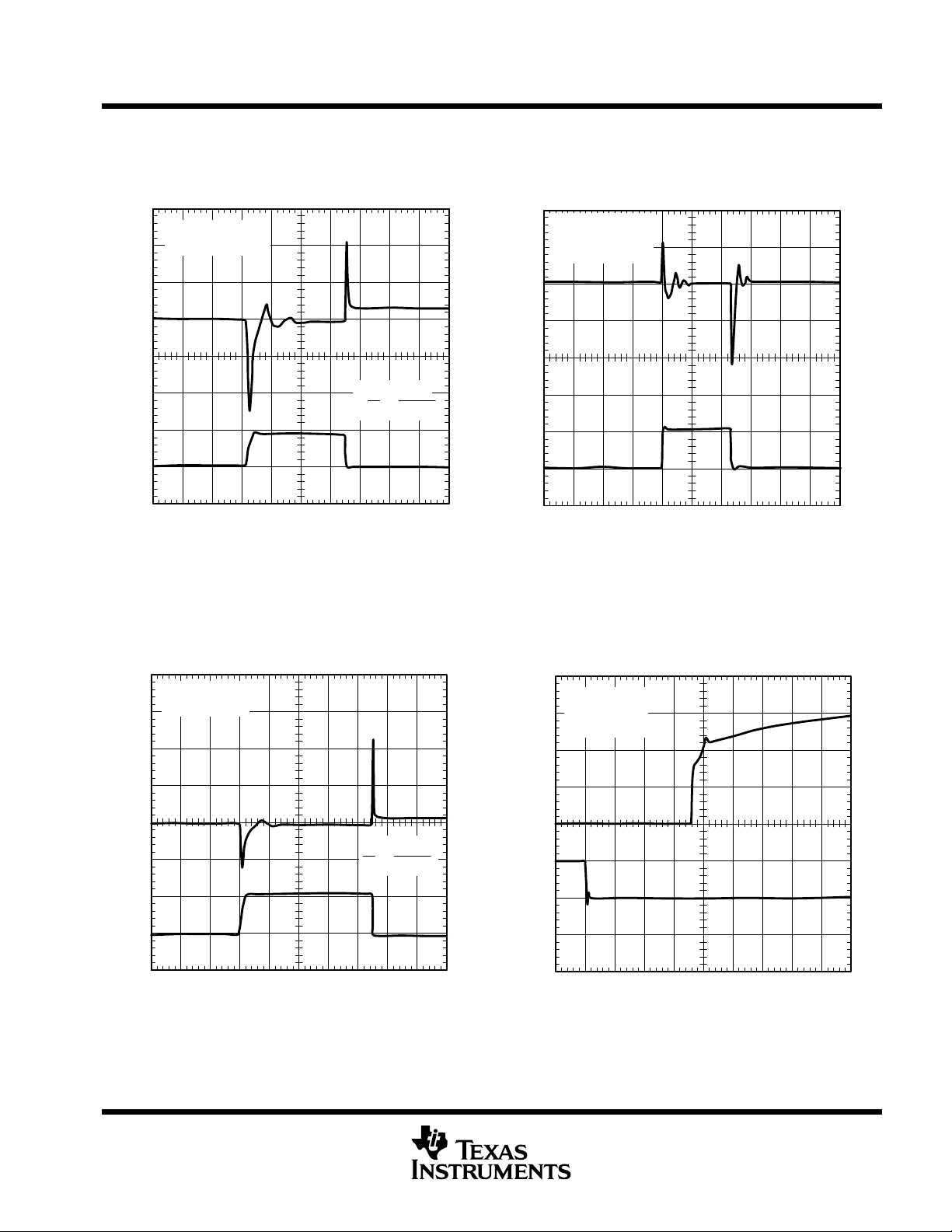
LINE TRANSIENT RESPONSE
VO = 1.5 V
IO = 5 A
50
Co = 100 µF
0
– Change in
O
–50
V
∆
Output Voltage – mV
–100
3.8
2.8
– Input Voltage – V
I
V
0 15010050 200 250 350300 400 450 500
t – Time – µs
Figure 13
10
POST OFFICE BOX 655303 • DALLAS, TEXAS 75265
Page 11
TPS75515, TPS75518, TPS75525, TPS75533 WITH POWER GOOD AND
I
TPS75501 FAST-TRANSIENT RESPONSE 5-A LOW-DROPOUT
VOLTAGE REGULATORS
SLVS293D – NOVEMBER 2000 – REVISED MAY 2002
TYPICAL CHARACTERISTICS
TPS75515
LOAD TRANSIENT RESPONSE
150
VO = 1.5 V
Co = 100 µF
50
0
di
dt
0604020 80 100 140120 160 180 200
t – Time – µs
–100
– Change in Output Voltage – mV
O
V
∆
–150
100
–50
Figure 14
TPS75533
LOAD TRANSIENT RESPONSE
+
1.25 A
µs
TPS75533
LINE TRANSIENT RESPONSE
100
VO = 3.3 V
IO = 5 A
50
Co = 100 µF
0
–50
–100
– Change in Output Voltage – mV
O
V
5
0
∆
O
I – Output Current – A
0 15010050 200 250 350300 400 450 500
t – Time – µs
5.3
4.3
– Input Voltage – V
V
Figure 15
TPS75533
OUTPUT VOLTAGE AND ENABLE VOLTAGE
vs
TIME (START-UP)
VO =3 .3 V
Co = 100 µF
200
100
0
di
–100
– Change in Output Voltage – mV
O
V
∆
0604020 80 100 140120 160 180 200
t – Time – µs
dt
Figure 16
+
1.25 A
µs
VI = 4.3 V
3.3
IO = 10 mA
TJ = 25°C
– Output Voltage – V
O
V
0
4.3
5
0
O
I – Output Current – A
0
Enable Voltage – V
0
0.2 10.4 0.6 0.8
t – Time (Start-Up) – ms
Figure 17
POST OFFICE BOX 655303 • DALLAS, TEXAS 75265
11
Page 12

TPS75515, TPS75518, TPS75525, TPS75533 WITH POWER GOOD AND
TPS75501 FAST-TRANSIENT RESPONSE 5-A LOW-DROPOUT
VOLTAGE REGULATORS
SLVS293D – NOVEMBER 2000 – REVISED MAY 2002
TYPICAL CHARACTERISTICS
+
C
ESR
To Load
o
R
L
V
I
IN
EN
OUT
GND
Figure 18. Test Circuit for Typical Regions of Stability (Figures 19 and 20) (Fixed Output Options)
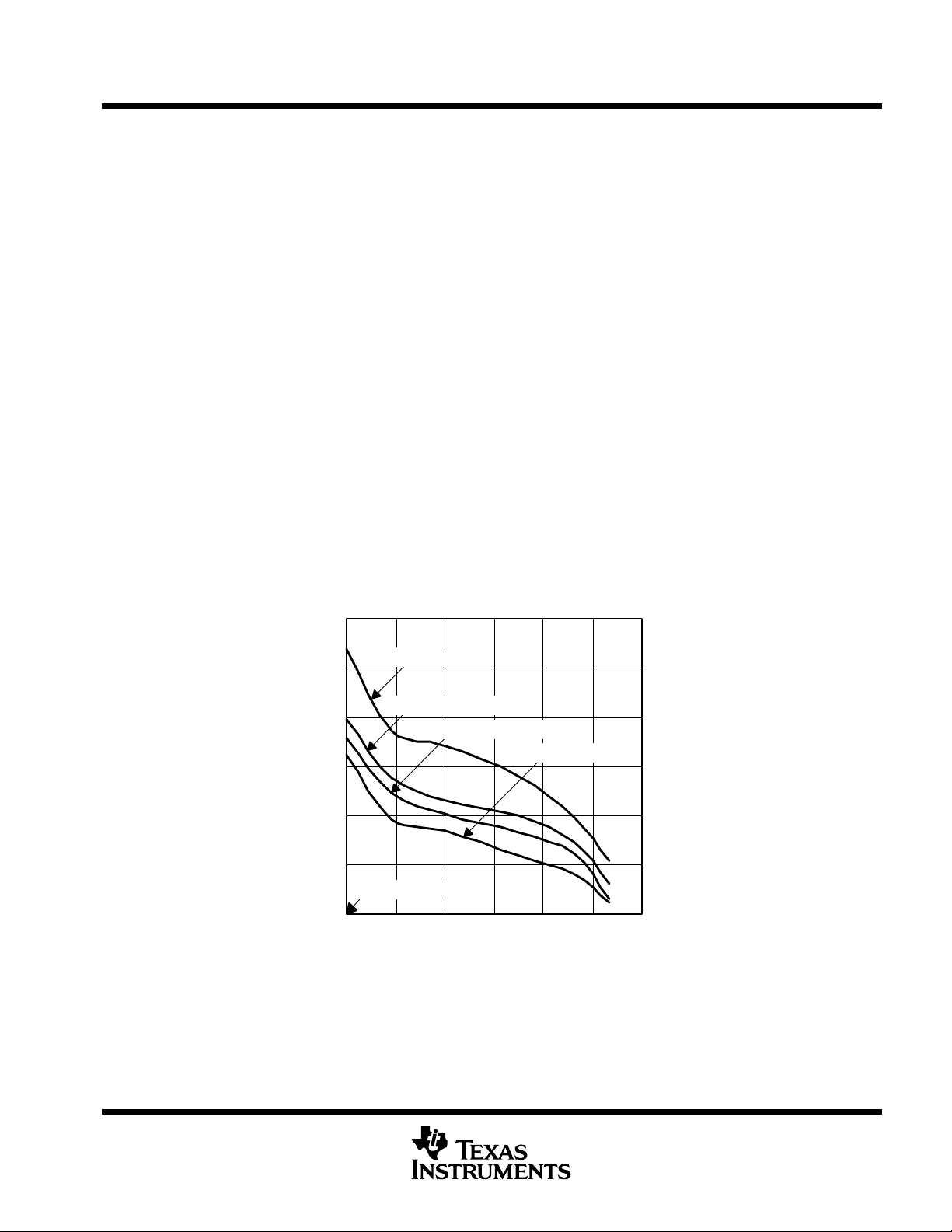
TYPICAL REGION OF STABILITY
EQUIVALENT SERIES RESISTANCE
vs
OUTPUT CURRENT
10
Co = 680 µF
TJ = 25°C
1
Region of Stability
†
10
1
TYPICAL REGION OF STABILITY
EQUIVALENT SERIES RESISTANCE
vs
OUTPUT CURRENT
Co = 47 µF
TJ = 25°C
Region of Stability
†
0.2
0.1
ESR – Equivalent Series Resistance –Ω
0.015
0.01
05
Region of Instability
1234
IO – Output Current – A
ESR – Equivalent Series Resistance –Ω
0.01
05
Figure 19
†
Equivalent series resistance (ESR) refers to the total series resistance, including the ESR of the capacitor, any series resistance added externally ,
and PWB trace resistance to Co.
Region of Instability
1234
IO – Output Current – A
Figure 20
12
POST OFFICE BOX 655303 • DALLAS, TEXAS 75265
Page 13

TPS75515, TPS75518, TPS75525, TPS75533 WITH POWER GOOD AND
TPS75501 FAST-TRANSIENT RESPONSE 5-A LOW-DROPOUT
VOLTAGE REGULATORS
SLVS293D – NOVEMBER 2000 – REVISED MAY 2002
THERMAL INFORMATION
The amount of heat that an LDO linear regulator generates is directly proportional to the amount of power it
dissipates during operation. All integrated circuits have a maximum allowable junction temperature (T
above which normal operation is not assured. A system designer must design the operating environment so
that the operating junction temperature (T
) does not exceed the maximum junction temperature (TJmax). The
J
two main environmental variables that a designer can use to improve thermal performance are air flow and
external heatsinks. The purpose of this information is to aid the designer in determining the proper operating
environment for a linear regulator that is operating at a specific power level.
max)
J
In general, the maximum expected power (P
PDmax +
ǒ
V
I(avg)
* V
O(avg)
Ǔ
I
O(avg)
) consumed by a linear regulator is computed as:
D(max)
) V
I(avg)
xI
(Q)
(1)
Where:
V
is the average input voltage.
I(avg)
V
I
O(avg)
I
(Q)
is the average output voltage.
O(avg)
is the average output current.
is the quiescent current.
For most TI LDO regulators, the quiescent current is insignificant compared to the average output current;
x I
therefore, the term V
I(avg)
the ambient temperature (T
can be neglected. The operating junction temperature is computed by adding
(Q)
) and the increase in temperature due to the regulator’s power dissipation. The
A
temperature rise is computed by multiplying the maximum expected power dissipation by the sum of the thermal
resistances between the junction and the case (R
(R
). Thermal resistances are measures of how effectively an object dissipates heat. T ypically , the larger the
θSA
), the case to heatsink (R
θJC
), and the heatsink to ambient
θCS
device, the more surface area available for power dissipation and the lower the object’s thermal resistance.
Figure 21 illustrates these thermal resistances for (a) a TO–220 package attached to a heatsink, and (b) a
TO–263 package mounted on a JEDEC High-K board.
C
B
T
A
J
R
R
R
θJC
θCS
θSA
A
T
B
C
C
TO–263 Package
T
A
(b)
B
C
A
TO–220 Package
(a)
Figure 21. Thermal Resistances
POST OFFICE BOX 655303 • DALLAS, TEXAS 75265
13
Page 14

TPS75515, TPS75518, TPS75525, TPS75533 WITH POWER GOOD AND
TPS75501 FAST-TRANSIENT RESPONSE 5-A LOW-DROPOUT
VOLTAGE REGULATORS
SLVS293D – NOVEMBER 2000 – REVISED MAY 2002
THERMAL INFORMATION
Equation 2 summarizes the computation:
TJ+ TA) P
The R
θJC
is specific to each regulator as determined by its package, lead frame, and die size provided in the
max xǒR
D
regulator’s datasheet. The R
) R
θJC
is a function of the type and size of heatsink. For example, black body radiator
θSA
θCS
) R
θSA
Ǔ
type heatsinks, like the one attached to the TO–220 package in Figure 21(a), can have R
from 5°C/W for very large heatsinks to 50°C/W for very small heatsinks. The R
is a function of how the
θCS
values ranging
θCS
(2)
package is attached to the heatsink. For example, if a thermal compound is used to attach a heatsink to a
TO–220 package, R
of 1°C/W is reasonable.
θCS
Even if no external black body radiator type heatsink is attached to the package, the board on which the regulator
is mounted will provide some heatsinking through the pin solder connections. Some packages, like the TO–263
and TI’s TSSOP PowerPAD packages, use a copper plane underneath the package or the circuit board’s
ground plane for additional heatsinking to improve their thermal performance. Computer aided thermal
modeling can be used to compute very accurate approximations of an integrated circuit’s thermal performance
in different operating environments (e.g., different types of circuit boards, different types and sizes of heatsinks,
and different air flows, etc.). Using these models, the three thermal resistances can be combined into one
thermal resistance between junction and ambient (R
). This R
θJA
is valid only for the specific operating
θJA
environment used in the computer model.
Equation 2 simplifies into equation 3:
TJ+ TA) P
max x R
D
θJA
(3)
Rearranging equation 3 gives equation 4:
TJ–T
R
θJA
+
A
PDmax
(4)
Using equation 3 and the computer model generated curves shown in Figures 22 and 25, a designer can quickly
compute the required heatsink thermal resistance/board area for a given ambient temperature, power
dissipation, and operating environment.
PowerPAD is a trademark of Texas Instruments.
14
POST OFFICE BOX 655303 • DALLAS, TEXAS 75265
Page 15
TPS75515, TPS75518, TPS75525, TPS75533 WITH POWER GOOD AND
TPS75501 FAST-TRANSIENT RESPONSE 5-A LOW-DROPOUT
VOLTAGE REGULATORS
SLVS293D – NOVEMBER 2000 – REVISED MAY 2002
THERMAL INFORMATION
TO–220 power dissipation
The TO–220 package provides an effective means of managing power dissipation in through-hole applications.
The TO–220 package dimensions are provided in the Mechanical Data section at the end of the data sheet. A
heatsink can be used with the TO–220 package to effectively lower the junction-to-ambient thermal resistance.
To illustrate, the TPS75525 in a TO–220 package was chosen. For this example, the average input voltage is
3.3 V , the output voltage is 2.5 V, the average output current is 3 A, the ambient temperature 55°C, the air flow
is 150 LFM, and the operating environment is the same as documented below. Neglecting the quiescent current,
the maximum average power is:
P
max +(3.3 – 2.5)Vx3A + 2.4 W
D
(5)
Substituting TJmax for TJ into equation 4 gives equation 6:
R
max + (125 – 55)°Cń2.4 W + 29°CńW
θJA
From Figure 22, R
vs Heatsink Thermal Resistance, a heatsink with R
θJA
= 22°C/W is required to dissipate
θSA
(6)
2.4 W. The model operating environment used in the computer model to construct Figure 22 consisted of a
standard JEDEC High-K board (2S2P) with a 1 oz. internal copper plane and ground plane. Since the package
pins were soldered to the board, 450 mm
2
of the board was modeled as a heatsink. Figure 23 shows the side
view of the operating environment used in the computer model.
THERMAL RESISTANCE
vs
HEATSINK THERMAL RESISTANCE
65
Natural Convection
55
°
45
35
Air Flow = 150 LFM
Air Flow = 250 LFM
Air Flow = 500 LFM
– Thermal Resistance –
θJA
R C/W
25
15
No Heatsink
5
R
– Heatsink Thermal Resistance – °C/W
θSA
Figure 22
POST OFFICE BOX 655303 • DALLAS, TEXAS 75265
0510152025
15
Page 16

TPS75515, TPS75518, TPS75525, TPS75533 WITH POWER GOOD AND
TPS75501 FAST-TRANSIENT RESPONSE 5-A LOW-DROPOUT
VOLTAGE REGULATORS
SLVS293D – NOVEMBER 2000 – REVISED MAY 2002
THERMAL INFORMATION
TO–220 power dissipation (continued)
0.21 mm
1 oz. Copper
Ground Plane
0.21 mm
1 oz. Copper
Power Plane
Figure 23
From the data in Figure 22 and rearranging equation 4, the maximum power dissipation for a different heatsink
R
and a specific ambient temperature can be computed (see Figure 24).
θSA
POWER DISSIPATION
vs
HEATSINK THERMAL RESISTANCE
10
TA = 55°C
Air Flow = 500 LFM
16
– Power Dissipation Limit – W
P
Air Flow = 250 LFM
Air Flow = 150 LFM
D
No Heatsink
1
R
– Heatsink Thermal Resistance – °C/W
θSA
Natural Convection
01020
Figure 24
POST OFFICE BOX 655303 • DALLAS, TEXAS 75265
Page 17

TPS75515, TPS75518, TPS75525, TPS75533 WITH POWER GOOD AND
TPS75501 FAST-TRANSIENT RESPONSE 5-A LOW-DROPOUT
VOLTAGE REGULATORS
SLVS293D – NOVEMBER 2000 – REVISED MAY 2002
THERMAL INFORMATION
TO–263 power dissipation
The TO–263 package provides an effective means of managing power dissipation in surface mount
applications. The TO–263 package dimensions are provided in the Mechanical Data section at the end of the
data sheet. The addition of a copper plane directly underneath the TO–263 package enhances the thermal
performance of the package.
To illustrate, the TPS75525 in a TO–263 package was chosen. For this example, the average input voltage is
3.3 V , the output voltage is 2.5 V, the average output current is 3 A, the ambient temperature 55°C, the air flow
is 150 LFM, and the operating environment is the same as documented below. Neglecting the quiescent current,
the maximum average power is:
P
max +(3.3 – 2.5)Vx3A + 2.4 W
D
(7)
Substituting TJmax for TJ into equation 4 gives equation 8:
R
max + (125 – 55)°Cń2.4 W + 29°CńW
θJA
From Figure 25, R
vs Copper Heatsink Area, the ground plane needs to be 2 cm2 for the part to dissipate
θJA
(8)
2.4 W. The model operating environment used in the computer model to construct Figure 25 consisted of a
standard JEDEC High-K board (2S2P) with a 1 oz. internal copper plane and ground plane. The package is
soldered to a 2 oz. copper pad. The pad is tied through thermal vias to the 1 oz. ground plane. Figure 26 shows
the side view of the operating environment used in the computer model.
THERMAL RESISTANCE
vs
COPPER HEATSINK AREA
40
No Air Flow
35
°
150 LFM
30
250 LFM
25
– Thermal Resistance –
θJA
20
R C/W
15
0 0.01 0.1 1 10 100
Copper Heatsink Area – cm
Figure 25
POST OFFICE BOX 655303 • DALLAS, TEXAS 75265
2
17
Page 18

TPS75515, TPS75518, TPS75525, TPS75533 WITH POWER GOOD AND
TPS75501 FAST-TRANSIENT RESPONSE 5-A LOW-DROPOUT
VOLTAGE REGULATORS
SLVS293D – NOVEMBER 2000 – REVISED MAY 2002
THERMAL INFORMATION
TO–263 power dissipation (continued)
2 oz. Copper Solder Pad
with 25 Thermal Vias
1 oz. Copper
Power Plane
1 oz. Copper
Ground Plane
Thermal Vias, 0.3 mm
Diameter, 1.5 mm Pitch
Figure 26
From the data in Figure 25 and rearranging equation 4, the maximum power dissipation for a different ground
plane area and a specific ambient temperature can be computed (see Figure 27).
MAXIMUM POWER DISSIPATION
vs
COPPER HEATSINK AREA
5
TA = 55°C
4
3
2
– Maximum Power Dissipation – W
D
P
1
0 0.01 0.1 1 10 100
Copper Heatsink Area – cm
250 LFM
150 LFM
No Air Flow
2
18
Figure 27
POST OFFICE BOX 655303 • DALLAS, TEXAS 75265
Page 19

TPS75515, TPS75518, TPS75525, TPS75533 WITH POWER GOOD AND
)
TPS75501 FAST-TRANSIENT RESPONSE 5-A LOW-DROPOUT
VOLTAGE REGULATORS
SLVS293D – NOVEMBER 2000 – REVISED MAY 2002
APPLICATION INFORMATION
programming the TPS75501 adjustable LDO regulator
The output voltage of the TPS75501 adjustable regulator is programmed using an external resistor divider as
shown in Figure 28. The output voltage is calculated using:
R1
VO+ V
ref
ǒ
1 )
Where:
V
= 1.224 V typ (the internal reference voltage)
ref
Resistors R1 and R2 should be chosen for approximately 40-µA divider current. Lower value resistors can be
used but offer no inherent advantage and waste more power. Higher values should be avoided as leakage
currents at FB increase the output voltage error. The recommended design procedure is to choose
R2 = 30.1 kΩ to set the divider current at 40 µA and then calculate R1 using:
V
ǒ
V
ref
O
* 1Ǔ R2
≥ 2 V
R1 +
V
I
1 µF
≤ 0.7 V
R2
TPS75501
IN
EN
GND
Ǔ
OUT
FB
R2
R1
OUTPUT VOLTAGE
PROGRAMMING GUIDE
OUTPUT
V
O
C
o
VOLTAGE
2.5 V
3.3 V
3.6 V
R1 R2
31.6
51
58.3
30.1
30.1
30.1
(9
(10)
UNIT
kΩ
kΩ
kΩ
Figure 28. TPS75501 Adjustable LDO Regulator Programming
regulator protection
The TPS755xx PMOS-pass transistor has a built-in back diode that conducts reverse currents when the input
voltage drops below the output voltage (e.g., during power down). Current is conducted from the output to the
input and is not internally limited. When extended reverse voltage is anticipated, external limiting may be
appropriate.
The TPS755xx also features internal current limiting and thermal protection. During normal operation, the
TPS755xx limits output current to approximately 10 A. When current limiting engages, the output voltage scales
back linearly until the overcurrent condition ends. While current limiting is designed to prevent gross device
failure, care should be taken not to exceed the power dissipation ratings of the package. If the temperature of
the device exceeds 150°C(typ), thermal-protection circuitry shuts it down. Once the device has cooled below
130°C(typ), regulator operation resumes.
POST OFFICE BOX 655303 • DALLAS, TEXAS 75265
19
Page 20

TPS75515, TPS75518, TPS75525, TPS75533 WITH POWER GOOD AND
TPS75501 FAST-TRANSIENT RESPONSE 5-A LOW-DROPOUT
VOLTAGE REGULATORS
SLVS293D – NOVEMBER 2000 – REVISED MAY 2002
APPLICATION INFORMATION
input capacitor
For a typical application, a ceramic input bypass capacitor (0.22 µF–1 µF) is recommended to ensure device
stability . This capacitor should be as close as possible to the input pin. Due to the impedance of the input supply,
large transient currents will cause the input voltage to droop. If this droop causes the input voltage to drop below
the UVLO threshold, the device will turn off. Therefore, it is recommended that a larger capacitor be placed in
parallel with the ceramic bypass capacitor at the regulator’s input. The size of this capacitor depends on the
output current, response time of the main power supply , and the main power supply’s distance to the regulator .
At a minimum, the capacitor should be sized to ensure that the input voltage does not drop below the minimum
UVLO threshold voltage during normal operating conditions.
output capacitor
As with most LDO regulators, the TPS755xx requires an output capacitor connected between OUT and GND
to stabilize the internal control loop. The minimum recommended capacitance value is 47 µF with an ESR
(equivalent series resistance) of at least 200 mΩ. As shown in Figure 29, most capacitor and ESR combinations
with a product of 47e–6 x 0.2 = 9.4e–6 or larger will be stable, provided the capacitor value is at least 47 µF.
Solid tantalum electrolytic and aluminum electrolytic capacitors are all suitable, provided they meet the
requirements described in this section. Larger capacitors provide a wider range of stability and better load
transient response.
This information along with the ESR graphs, Figures 19, 20, and 29, is included to assist in selection of suitable
capacitance for the user’s application. When necessary to achieve low height requirements along with high
output current and/or high load capacitance, several higher ESR capacitors can be used in parallel to meet
these guidelines.
OUTPUT CAPACITANCE
vs
EQUIVALENT SERIES RESISTANCE
1000
Region of Stability
ESR min x Co = Constant
100
47
Output Capacitance – Fµ
Region of Instability
Y = ESRmin x C
10
0.01
ESR – Equivalent Series Resistance – Ω
o
0.1
0.2
Figure 29
20
POST OFFICE BOX 655303 • DALLAS, TEXAS 75265
Page 21

TPS75515, TPS75518, TPS75525, TPS75533 WITH POWER GOOD AND
TPS75501 FAST-TRANSIENT RESPONSE 5-A LOW-DROPOUT
VOLTAGE REGULATORS
SLVS293D – NOVEMBER 2000 – REVISED MAY 2002
MECHANICAL DATA
KC (R-PSFM-T5) PLASTIC FLANGE-MOUNT
0.156 (3,96)
0.146 (3,71)
0.125 (3,18)
(see Note C)
DIA
1
0.420 (10,67)
0.380 (9,65)
5
0.113 (2,87)
0.103 (2,62)
0.147 (3,73)
0.137 (3,48)
0.185 (4,70)
0.175 (4,46)
0.340 (8,64)
0.330 (8,38)
0.055 (1,40)
0.045 (1,14)
1.010 (25,64)
0.990 (25,14)
0.040 (1,02)
0.030 (0,76)
0.010 (0,25)
NOTES: A. All linear dimensions are in inches (millimeters).
B. This drawing is subject to change without notice.
C. Lead dimensions are not controlled within this area.
D. All lead dimensions apply before solder dip.
E. The center lead is in electrical contact with the mounting tab.
M
POST OFFICE BOX 655303 • DALLAS, TEXAS 75265
0.067 (1,70)
0.268 (6,81)
0.122 (3,10)
0.102 (2,59)
0.025 (0,64)
0.012 (0,30)
4040208/D 01/00
21
Page 22

TPS75515, TPS75518, TPS75525, TPS75533 WITH POWER GOOD AND
TPS75501 FAST-TRANSIENT RESPONSE 5-A LOW-DROPOUT
VOLTAGE REGULATORS
SLVS293D – NOVEMBER 2000 – REVISED MAY 2002
MECHANICAL DATA
KTT (R-PSFM-G5) PLASTIC FLANGE-MOUNT
0.610 (15,49)
0.590 (14,99)
0.067 (1,70)
0.268 (6,81)
1
0.405 (10,29)
0.395 (10,03)
5
0.035 (0,89)
0.029 (0,74)
0.058 (1,47)
0.052 (1,32)
0.340 (8,64)
0.330 (8,38)
0.010 (0,25)
0.185 (4,70)
0.175 (4,45)
0.050 (1,27) NOM
0.107 (2,72)
0.103 (2,62)
0.010 (0,25)
0.001 (0,03)
Seating Plane
0.004 (0,10)
M
NOTES: A. All linear dimensions are in inches (millimeters).
B. This drawing is subject to change without notice.
C. Dimensions do not include mold protrusions, not to exceed 0.006 (0,15).
0.021 (0,53)
0.015 (0,38)
0.110 (2,79)
0.090 (2,29)
0°–ā5°
4200577/A 09/99
22
POST OFFICE BOX 655303 • DALLAS, TEXAS 75265
Page 23

PACKAGE OPTION ADDENDUM
www.ti.com
PACKAGING INFORMATION
Orderable Device Status
TPS75501KC ACTIVE TO-220 KC 5 50 Green(RoHS &
TPS75501KTT OBSOLETE DDPAK/
TPS75501KTTR ACTIVE DDPAK/
TPS75501KTTRG3 ACTIVE DDPAK/
TPS75501KTTT ACTIVE DDPAK/
TPS75515KC ACTIVE TO-220 KC 5 50 Green(RoHS &
TPS75515KTT OBSOLETE DDPAK/
TPS75515KTTR ACTIVE DDPAK/
TPS75515KTTT ACTIVE DDPAK/
TPS75518KC ACTIVE TO-220 KC 5 50 Green(RoHS &
TPS75518KCG3 ACTIVE TO-220 KC 5 50 Green (RoHS &
TPS75518KTT OBSOLETE DDPAK/
TPS75518KTTR ACTIVE DDPAK/
TPS75518KTTT ACTIVE DDPAK/
TPS75525KC ACTIVE TO-220 KC 5 50 Green(RoHS &
TPS75525KTT OBSOLETE DDPAK/
TPS75525KTTR ACTIVE DDPAK/
TPS75525KTTT ACTIVE DDPAK/
TPS75533KC ACTIVE TO-220 KC 5 50 Green(RoHS &
TPS75533KCG3 ACTIVE TO-220 KC 5 50 Green (RoHS &
TPS75533KTT OBSOLETE DDPAK/
TPS75533KTTR ACTIVE DDPAK/
TPS75533KTTRG3 ACTIVE DDPAK/
TPS75533KTTT ACTIVE DDPAK/
(1)
The marketing status values are defined as follows:
(1)
Package
Type
TO-263
TO-263
TO-263
TO-263
TO-263
TO-263
TO-263
TO-263
TO-263
TO-263
TO-263
TO-263
TO-263
TO-263
TO-263
TO-263
TO-263
Package
Drawing
KTT 5 TBD Call TI Call TI
KTT 5 500 Green (RoHS &
KTT 5 500 Green (RoHS &
KTT 5 50 Green (RoHS &
KTT 5 TBD Call TI Call TI
KTT 5 500 Green (RoHS &
KTT 5 50 TBD CU SN Level-2-220C-1 YEAR
KTT 5 TBD Call TI Call TI
KTT 5 500 Green (RoHS &
KTT 5 50 Green (RoHS &
KTT 5 TBD Call TI Call TI
KTT 5 500 Green (RoHS &
KTT 5 50 Green (RoHS &
KTT 5 TBD Call TI Call TI
KTT 5 500 Green (RoHS &
KTT 5 500 Green (RoHS &
KTT 5 50 Green (RoHS &
Pins Package
Qty
Eco Plan
no Sb/Br)
no Sb/Br)
no Sb/Br)
no Sb/Br)
no Sb/Br)
no Sb/Br)
no Sb/Br)
no Sb/Br)
no Sb/Br)
no Sb/Br)
no Sb/Br)
no Sb/Br)
no Sb/Br)
no Sb/Br)
no Sb/Br)
no Sb/Br)
no Sb/Br)
no Sb/Br)
(2)
Lead/Ball Finish MSL Peak Temp
CU SN Level-NC-NC-NC
CU SN Level-2-260C-1 YEAR
CU SN Level-2-260C-1 YEAR
CU SN Level-2-260C-1 YEAR
CU SN Level-NC-NC-NC
CU SN Level-2-260C-1 YEAR
CU SN Level-NC-NC-NC
CU SN Level-NC-NC-NC
CU SN Level-2-260C-1 YEAR
CU SN Level-2-260C-1 YEAR
CU SN Level-NC-NC-NC
CU SN Level-2-260C-1 YEAR
CU SN Level-2-260C-1 YEAR
CU SN Level-NC-NC-NC
CU SN Level-NC-NC-NC
CU SN Level-2-260C-1 YEAR
CU SN Level-2-260C-1 YEAR
CU SN Level-2-260C-1 YEAR
8-Aug-2005
(3)
Addendum-Page 1
Page 24

PACKAGE OPTION ADDENDUM
www.ti.com
ACTIVE: Product device recommended for new designs.
LIFEBUY: TI has announced that the device will be discontinued, and a lifetime-buy period is in effect.
NRND: Not recommended for new designs. Device is in production to support existing customers, but TI does not recommend using this part in
a new design.
PREVIEW: Device has been announced but is not in production. Samples may or may not be available.
OBSOLETE: TI has discontinued the production of the device.
(2)
Eco Plan - The planned eco-friendly classification: Pb-Free (RoHS) or Green (RoHS & no Sb/Br) - please check
http://www.ti.com/productcontent for the latest availability information and additional product content details.
TBD: The Pb-Free/Green conversion plan has not been defined.
Pb-Free (RoHS): TI's terms "Lead-Free" or "Pb-Free" mean semiconductor products that are compatible with the current RoHS requirements
for all 6 substances, including the requirement that lead not exceed 0.1% by weight in homogeneous materials. Where designed to be soldered
at high temperatures, TI Pb-Free products are suitable for use in specified lead-free processes.
Green (RoHS & no Sb/Br): TI defines "Green" to mean Pb-Free (RoHS compatible), and free of Bromine (Br) and Antimony (Sb) based flame
retardants (Br or Sb do not exceed 0.1% by weight in homogeneous material)
(3)
MSL, Peak Temp. -- The Moisture Sensitivity Level rating according to the JEDEC industry standard classifications, and peak solder
temperature.
Important Information and Disclaimer:The information provided on this page represents TI's knowledge and belief as of the date that it is
provided. TI bases its knowledge and belief on information provided by third parties, and makes no representation or warranty as to the
accuracy of such information. Efforts are underway to better integrate information from third parties. TI has taken and continues to take
reasonable steps to provide representative and accurate information but may not have conducted destructive testing or chemical analysis on
incoming materials and chemicals. TI and TI suppliers consider certain information to be proprietary, and thus CAS numbers and other limited
information may not be available for release.
In no event shall TI's liability arising out of such information exceed the total purchase price of the TI part(s) at issue in this document sold by TI
to Customer on an annual basis.
8-Aug-2005
Addendum-Page 2
Page 25

Page 26

MECHANICAL DATA
MSOT008B – JANUARY 1995 – REVISED SEPTEMBER 2000
KC (R-PSFM-T5) PLASTIC FLANGE-MOUNT
0.156 (3,96)
0.146 (3,71)
0.125 (3,18)
(see Note C)
DIA
0.420 (10,67)
0.380 (9,65)
0.113 (2,87)
0.103 (2,62)
0.147 (3,73)
0.137 (3,48)
0.185 (4,70)
0.175 (4,46)
0.340 (8,64)
0.330 (8,38)
0.055 (1,40)
0.045 (1,14)
1.037 (26,34)
0.997 (25,32)
1
0.040 (1,02)
0.030 (0,76)
0.010 (0,25)
NOTES: A. All linear dimensions are in inches (millimeters).
B. This drawing is subject to change without notice.
C. Lead dimensions are not controlled within this area.
D. All lead dimensions apply before solder dip.
E. The center lead is in electrical contact with the mounting tab.
M
5
0.067 (1,70)
0.268 (6,81)
0.122 (3,10)
0.102 (2,59)
0.025 (0,64)
0.012 (0,30)
4040208/E 09/00
POST OFFICE BOX 655303 • DALLAS, TEXAS 75265
1
Page 27

IMPORTANT NOTICE
Texas Instruments Incorporated and its subsidiaries (TI) reserve the right to make corrections, modifications,
enhancements, improvements, and other changes to its products and services at any time and to discontinue
any product or service without notice. Customers should obtain the latest relevant information before placing
orders and should verify that such information is current and complete. All products are sold subject to TI’s terms
and conditions of sale supplied at the time of order acknowledgment.
TI warrants performance of its hardware products to the specifications applicable at the time of sale in
accordance with TI’s standard warranty. Testing and other quality control techniques are used to the extent TI
deems necessary to support this warranty . Except where mandated by government requirements, testing of all
parameters of each product is not necessarily performed.
TI assumes no liability for applications assistance or customer product design. Customers are responsible for
their products and applications using TI components. To minimize the risks associated with customer products
and applications, customers should provide adequate design and operating safeguards.
TI does not warrant or represent that any license, either express or implied, is granted under any TI patent right,
copyright, mask work right, or other TI intellectual property right relating to any combination, machine, or process
in which TI products or services are used. Information published by TI regarding third-party products or services
does not constitute a license from TI to use such products or services or a warranty or endorsement thereof.
Use of such information may require a license from a third party under the patents or other intellectual property
of the third party, or a license from TI under the patents or other intellectual property of TI.
Reproduction of information in TI data books or data sheets is permissible only if reproduction is without
alteration and is accompanied by all associated warranties, conditions, limitations, and notices. Reproduction
of this information with alteration is an unfair and deceptive business practice. TI is not responsible or liable for
such altered documentation.
Resale of TI products or services with statements different from or beyond the parameters stated by TI for that
product or service voids all express and any implied warranties for the associated TI product or service and
is an unfair and deceptive business practice. TI is not responsible or liable for any such statements.
Following are URLs where you can obtain information on other Texas Instruments products and application
solutions:
Products Applications
Amplifiers amplifier.ti.com Audio www.ti.com/audio
Data Converters dataconverter.ti.com Automotive www.ti.com/automotive
DSP dsp.ti.com Broadband www.ti.com/broadband
Interface interface.ti.com Digital Control www.ti.com/digitalcontrol
Logic logic.ti.com Military www.ti.com/military
Power Mgmt power.ti.com Optical Networking www.ti.com/opticalnetwork
Microcontrollers microcontroller.ti.com Security www.ti.com/security
Telephony www.ti.com/telephony
Video & Imaging www.ti.com/video
Wireless www.ti.com/wireless
Mailing Address: Texas Instruments
Post Office Box 655303 Dallas, Texas 75265
Copyright 2005, Texas Instruments Incorporated
 Loading...