

Texas Instruments TPS75133QPWP, TPS75125QPWPR, TPS75125QPWP, TPS75118QPWP, TPS75118QPWPR Datasheet
...
K
K
TPS75101Q, TPS75115Q, TPS75118Q, TPS75125Q, TPS75133Q WITH POWER GOOD
TPS75301Q, TPS75315Q, TPS75318Q, TPS75325Q, TPS75333Q WITH RESET
FAST-TRANSIENT-RESPONSE 1.5-A LOW-DROPOUT VOLTAGE REGULATORS
SLVS241 – MARCH 2000
D
1.5-A Low-Dropout Voltage Regulator
D
Available in 1.5-V, 1.8-V, 2.5-V, 3.3-V, Fixed
Output and Adjustable Versions
D
Open Drain Power-Good (PG) Status
Output (TPS751xxQ)
D
Open Drain Power-On Reset With 100-ms
Delay (TPS753xxQ)
D
Dropout Voltage Typically 160 mV at 1.5 A
(TPS75133Q)
D
Ultra Low 75 µA Typical Quiescent Current
D
Fast Transient Response
D
2% Tolerance Over Specified Conditions
For Fixed-Output Versions
D
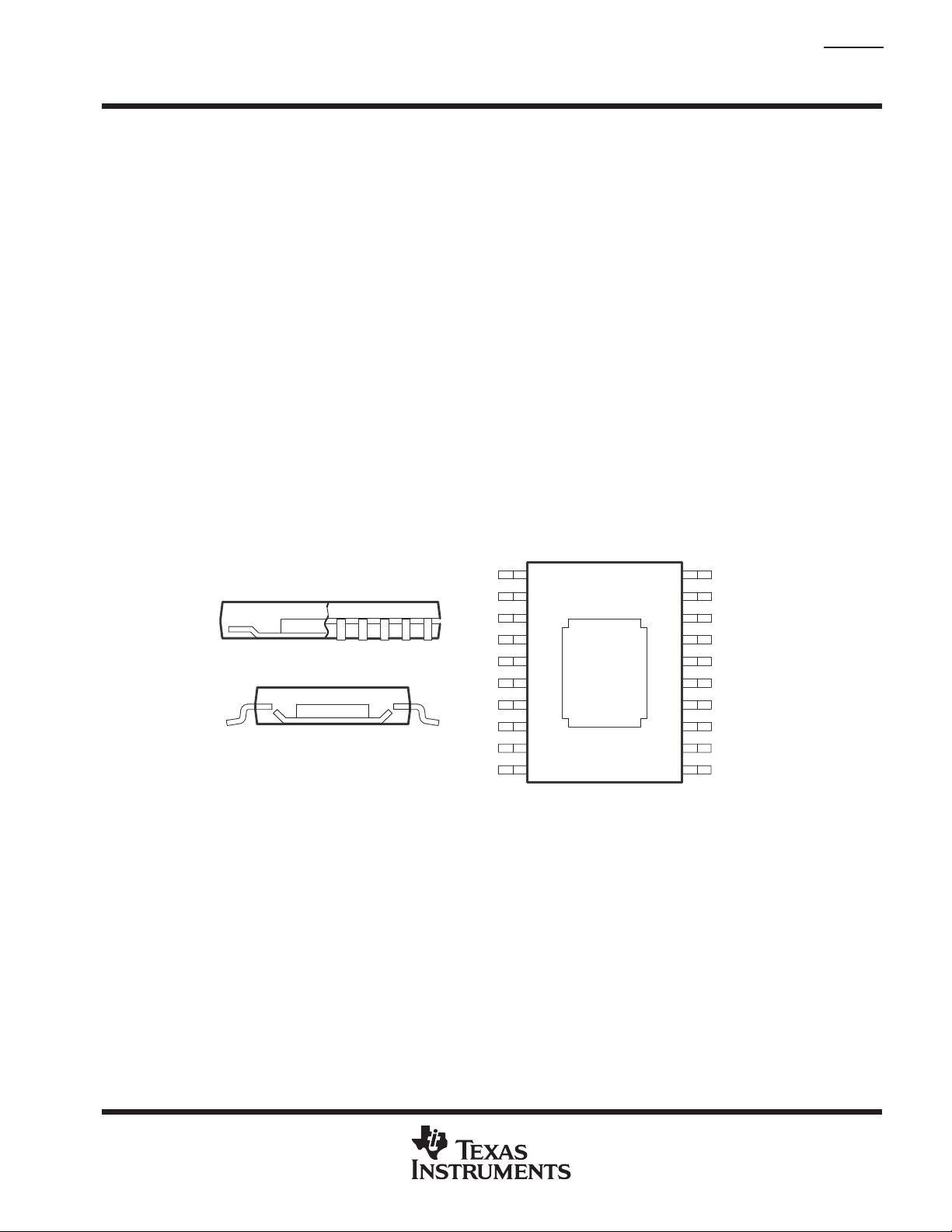
20-Pin TSSOP (PWP) PowerP AD Package
D
Thermal Shutdown Protection
GND/HEATSINK
NC
IN
IN
EN
PG or RESET
†
FB/SENSE
OUTPUT
OUTPUT
GND/HEATSINK
NC – No internal connection
†
PG is on the TPS751xx and RESET
PWP PACKAGE
(TOP VIEW)
1
2
3
4
5
6
7
8
9
10
is on the TPS753xx
20
19
18
17
16
15
14
13
12
11
GND/HEATSIN
NC
NC
GND
NC
NC
NC
NC
NC
GND/HEATSIN
description
The TPS753xxQ and TPS751xxQ are low dropout regulators with integrated power-on reset and power-good
(PG) functions respectively. These devices are capable of supplying 1.5 A of output current with a dropout of
160 mV (TPS75133Q, TPS75333Q). Quiescent current is 75 µA at full load and drops down to 1 µA when the
device is disabled. TPS751xxQ and TPS753xxQ are designed to have fast transient response for larger load
current changes.
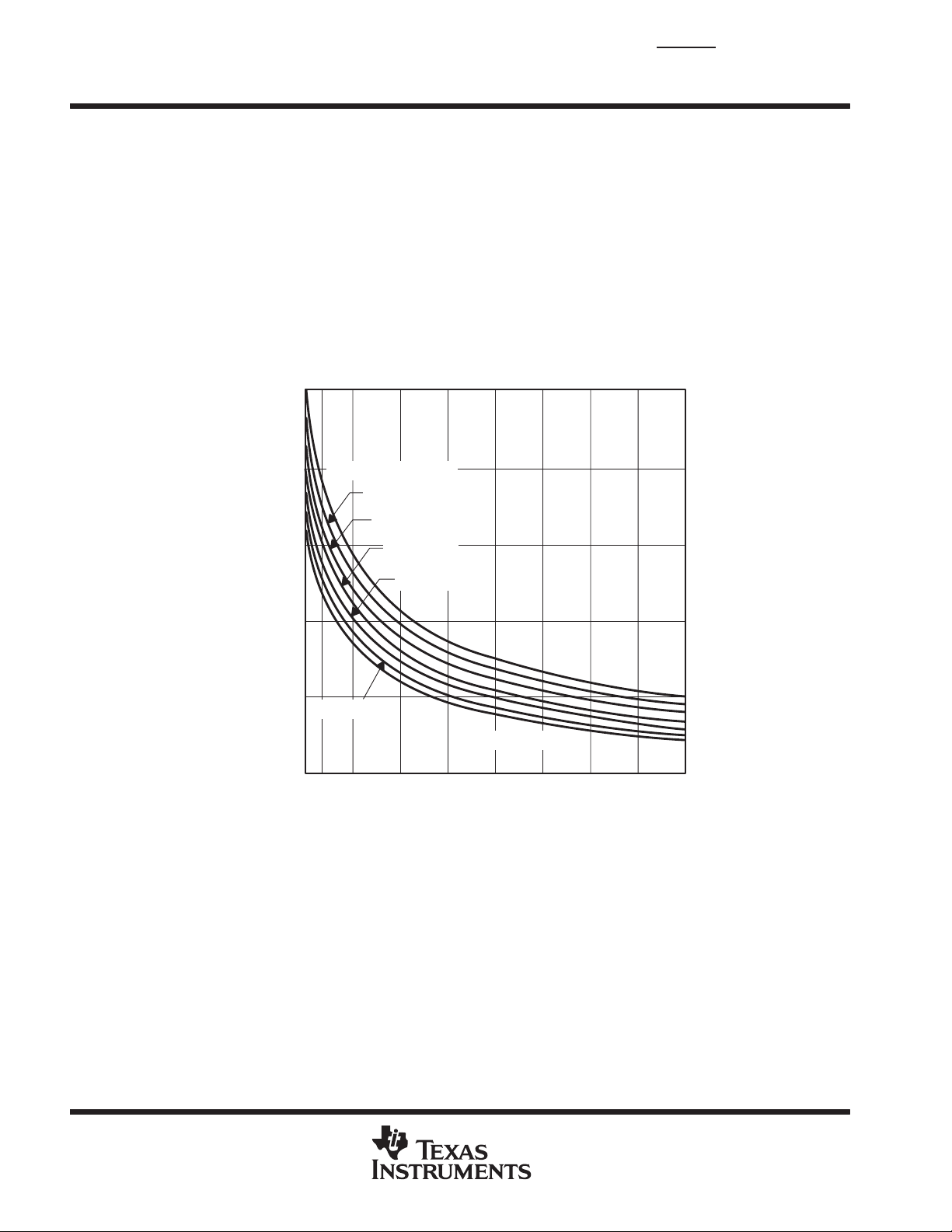
TPS75x33Q
DROPOUT VOLTAGE
TPS75x15Q
IL=1.5 A
CL=100 µF (T antalum)
VO=1.5 V
300
250
200
150
vs
JUNCTION TEMPERATURE
IO = 1.5 A
50
– Change in∆
O
–50
V
Output Voltage – mV
–100
LOAD TRANSIENT RESPONSE
0
100
– Dropout Voltage – mV
DO
V
50
0
–40 10 11060
Please be aware that an important notice concerning availability, standard warranty, and use in critical applications of
Texas Instruments semiconductor products and disclaimers thereto appears at the end of this data sheet.
PowerPAD is a trademark of Texas Instruments.
PRODUCTION DATA information is current as of publication date.
Products conform to specifications per the terms of Texas Instruments
standard warranty. Production processing does not necessarily include
testing of all parameters.
IO = 0.5 A
TJ – Junction Temperature – °C
–150
1.5
O
0
160
I – Output Current – A
032145768910
POST OFFICE BOX 655303 • DALLAS, TEXAS 75265
t – Time – ms
Copyright 2000, Texas Instruments Incorporated
1
TPS75101Q, TPS75115Q, TPS75118Q, TPS75125Q, TPS75133Q WITH POWER GOOD
T
TPS75301Q, TPS75315Q, TPS75318Q, TPS75325Q, TPS75333Q WITH RESET
FAST-TRANSIENT-RESPONSE 1.5-A LOW-DROPOUT VOLTAGE REGULATORS
SLVS241 – MARCH 2000
description (continued)
Because the PMOS device behaves as a low-value resistor, the dropout voltage is very low (typically 160 mV
at an output current of 1.5 A for the TPS75x33Q) and is directly proportional to the output current. Additionally ,
since the PMOS pass element is a voltage-driven device, the quiescent current is very low and independent
of output loading (typically 75 µA over the full range of output current, 1 mA to 1.5 A). These two key
specifications yield a significant improvement in operating life for battery-powered systems.
The device is enabled when EN
is connected to a low level voltage. This LDO family also features a sleep mode;
applying a TTL high signal to EN (enable) shuts down the regulator , reducing the quiescent current to less than
1 µA at TJ = 25°C.
For the TPS751xxQ, the power-good terminal (PG) is an active high, open drain output, which can be used to
implement a power-on reset or a low-battery indicator.
The RESET (SVS, POR, or power on reset) output of the TPS753xxQ initiates a reset in microcomputer and
microprocessor systems in the event of an undervoltage condition. An internal comparator in the TPS753xxQ
monitors the output voltage of the regulator to detect an undervoltage condition on the regulated output voltage.
When the output reaches 95% of its regulated voltage, RESET goes to a high-impedance state after a 100-ms
delay . RESET
goes to a logic-low state when the regulated output voltage is pulled below 95% (i.e., over load
condition) of its regulated voltage.
The TPS751xxQ or TPS753xxQ is offered in 1.5-V, 1.8-V, 2.5-V and 3.3-V fixed-voltage versions and in an
adjustable version (programmable over the range of 1.5 V to 5 V). Output voltage tolerance is specified as a
maximum of 2% over line, load, and temperature ranges. The TPS751xxQ and TPS753xxQ families are
available in 20-pin TSSOP (PWP) packages.
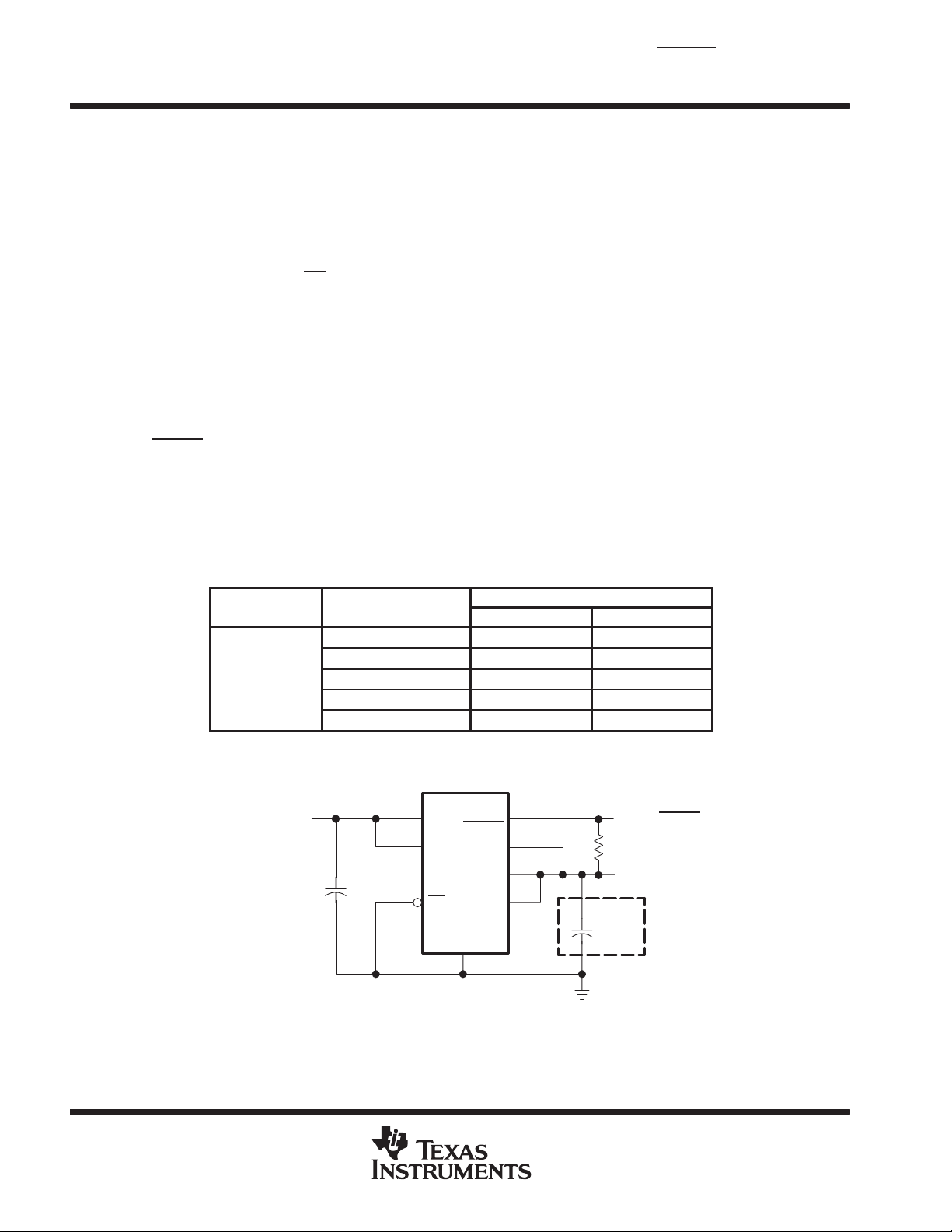
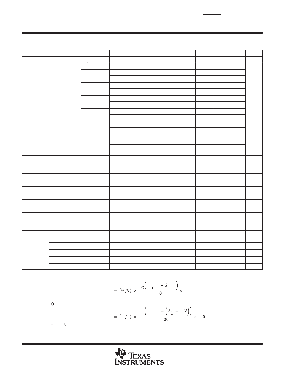
AVAILABLE OPTIONS
J
–40°C to 125°C
NOTE: The TPS75x01 is programmable using an external resistor divider (see application
information). The PWP package is available taped and reeled. Add an R suffix to the
device type (e.g., TPS75201QPWPR) to indicate tape and reel.
OUTPUT VOLTAGE
(TYP)
3.3 V TPS75133QPWP TPS75333QPWP
2.5 V TPS75125QPWP TPS75325QPWP
1.8 V TPS75118QPWP TPS75318QPWP
1.5 V TPS75115QPWP TPS75315QPWP
Adjustable 1.5 V to 5 V TPS75101QPWP TPS75301QPWP
TSSOP (PWP)
PG RESET
V
I
0.22 µF
†
See application information section for capacitor selection details.
3
IN
IN
EN
RESET
SENSE
GND
17
4
5
PG or
OUT
OUT
6
7
8
9
PG or RESET
V
O
†
C
O
+
47 µF
Output
Figure 1. Typical Application Configuration (For Fixed Output Options)
2
POST OFFICE BOX 655303 • DALLAS, TEXAS 75265
TPS75101Q, TPS75115Q, TPS75118Q, TPS75125Q, TPS75133Q WITH POWER GOOD
TPS75301Q, TPS75315Q, TPS75318Q, TPS75325Q, TPS75333Q WITH RESET
FAST-TRANSIENT-RESPONSE 1.5-A LOW-DROPOUT VOLTAGE REGULATORS
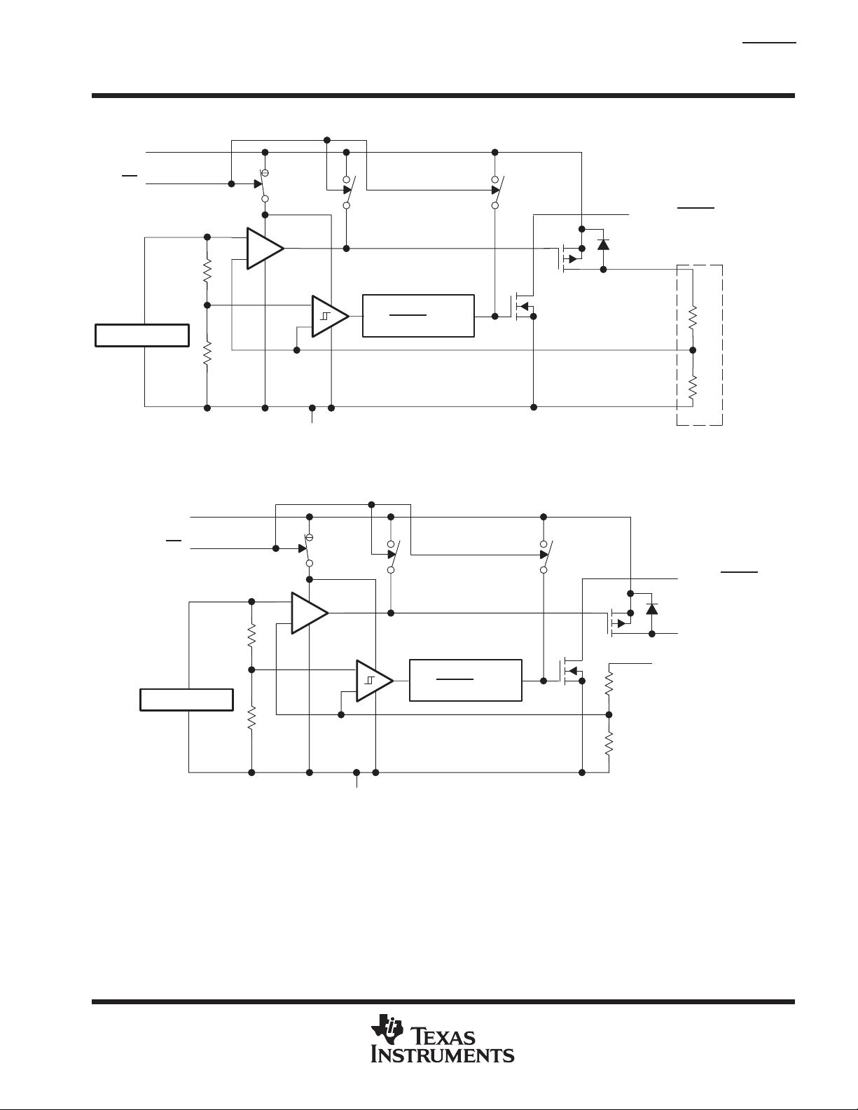
functional block diagram—adjustable version
IN
EN
_
SLVS241 – MARCH 2000
PG or RESET
+
V
= 1.1834 V
ref
+
_
GND
100 ms Delay
(for RESET
Option)
functional block diagram—fixed-voltage version
IN
EN
_
+
V
= 1.1834 V
ref
+
_
100 ms Delay
(for RESET
Option)
OUT
R1
FB
R2
External to the device
PG or RESET
OUT
SENSE
R1
GND
POST OFFICE BOX 655303 • DALLAS, TEXAS 75265
R2
3

TPS75101Q, TPS75115Q, TPS75118Q, TPS75125Q, TPS75133Q WITH POWER GOOD
I/O
DESCRIPTION
I/O
DESCRIPTION
TPS75301Q, TPS75315Q, TPS75318Q, TPS75325Q, TPS75333Q WITH RESET
FAST-TRANSIENT-RESPONSE 1.5-A LOW-DROPOUT VOLTAGE REGULATORS
SLVS241 – MARCH 2000
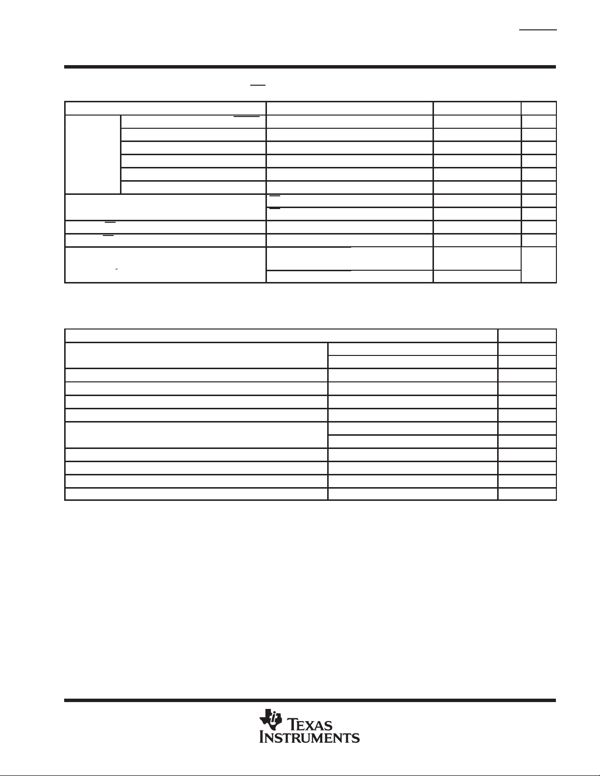
Terminal Functions (TPS751xxQ)
TERMINAL
NAME NO.
EN 5 I Enable Input
FB/SENSE 7 I Feedback input voltage for adjustable device (sense input for fixed options)
GND 17 Regulator Ground
GND/HEATSINK 1, 10, 11, 20 Ground/heatsink
IN 3, 4 I Input voltage
NC 2, 12, 13, 14,
15, 16, 18, 19
OUTPUT 8, 9 O Regulated output voltage
PG 6 O Power good output
TERMINAL
NAME NO.
EN 5 I Enable Input
FB/SENSE 7 I Feedback input voltage for adjustable device (sense input for fixed options)
GND 17 Regulator Ground
GND/HEATSINK 1, 10, 11, 20 Ground/heatsink
IN 3, 4 I Input voltage
NC 2, 12, 13, 14,
15, 16, 18, 19
OUTPUT 8, 9 O Regulated output voltage
RESET 6 O Reset output
No connection
Terminal Functions (TPS753xxQ)
No connection
4
POST OFFICE BOX 655303 • DALLAS, TEXAS 75265
TPS75101Q, TPS75115Q, TPS75118Q, TPS75125Q, TPS75133Q WITH POWER GOOD
TPS75301Q, TPS75315Q, TPS75318Q, TPS75325Q, TPS75333Q WITH RESET
FAST-TRANSIENT-RESPONSE 1.5-A LOW-DROPOUT VOLTAGE REGULATORS
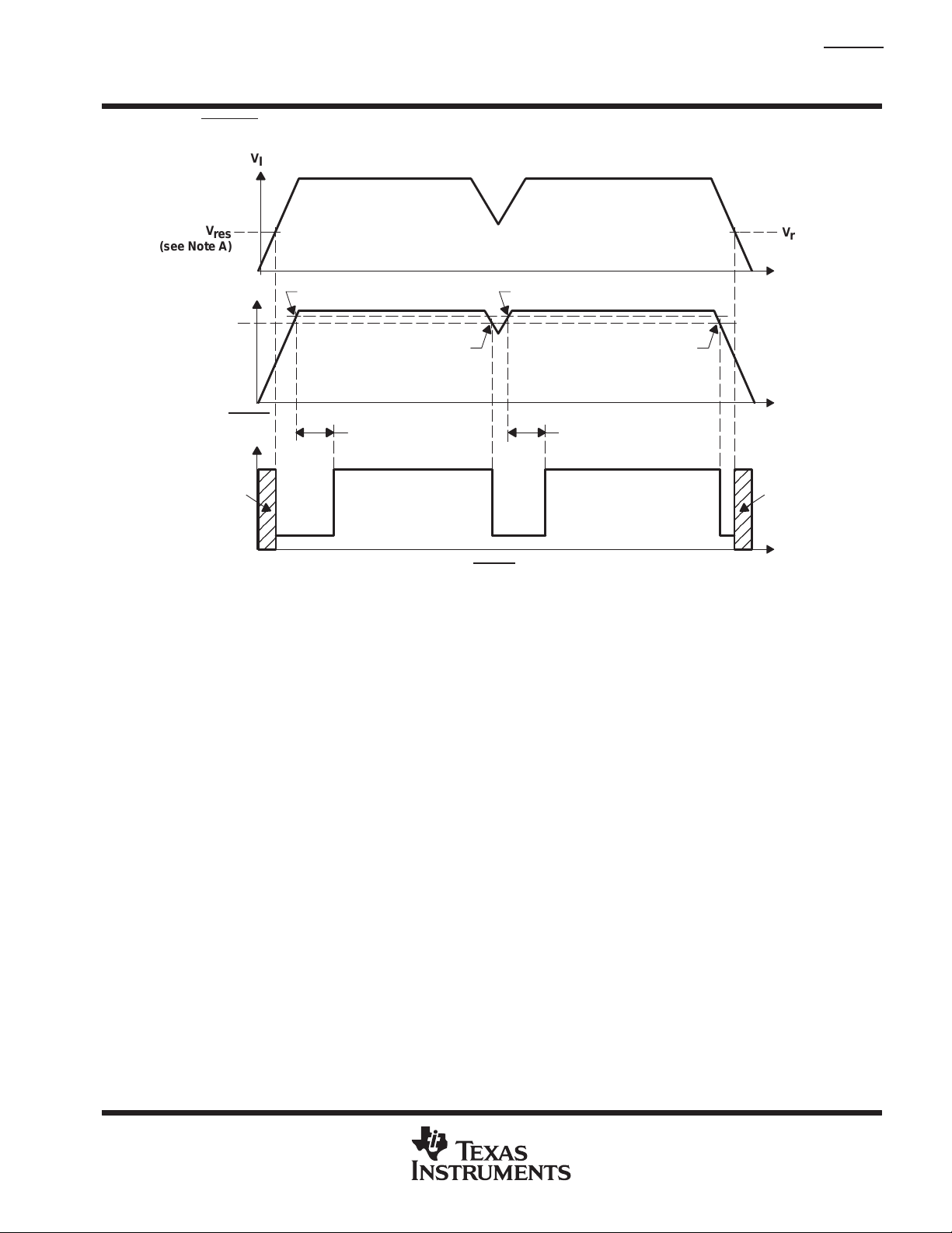
TPS753xxQ RESET timing diagram
V
I
SLVS241 – MARCH 2000
V
(see Note A)
NOTES: A. V
res
Threshold
Voltage
Output
Undefined
B. VIT –Trip voltage is typically 5% lower than the output voltage (95%VO) V
V
O
RESET
Output
is the minimum input voltage for a valid RESET. The symbol V
res
standards for semiconductor symbology.
V
(see Note B)
IT+
V
IT–
100 ms
Delay
(see Note B)
V
IT+
Less than 5% of the
output voltage
(see Note B)
100 ms
Delay
res
V
res
t
V
IT–
IT–
to V
is the hysteresis voltage.
IT+
t
Output
Undefined
t
(see Note B)
is not currently listed within EIA or JEDEC
POST OFFICE BOX 655303 • DALLAS, TEXAS 75265
5

TPS75101Q, TPS75115Q, TPS75118Q, TPS75125Q, TPS75133Q WITH POWER GOOD
TPS75301Q, TPS75315Q, TPS75318Q, TPS75325Q, TPS75333Q WITH RESET
FAST-TRANSIENT-RESPONSE 1.5-A LOW-DROPOUT VOLTAGE REGULATORS
SLVS241 – MARCH 2000
TPS751xxQ PG timing diagram
V
I
V
(see Note A)
NOTES: A. VPG is the minimum input voltage for a valid PG. The symbol VPG is not currently listed within EIA or JEDEC standards for
B. VIT –Trip voltage is typically 17% lower than the output voltage (83%VO) V
PG
V
O
Threshold
Voltage
PG
Output
Output
Undefined
semiconductor symbology .
V
(see Note B)
IT+
V
(see Note B)
IT–
V
(see Note B)
IT+
V
(see Note B)
IT–
to V
IT–
is the hysteresis voltage.
IT+
V
PG
t
t
Output
Undefined
t
6
POST OFFICE BOX 655303 • DALLAS, TEXAS 75265
PWP
§
PWP
¶
TPS75101Q, TPS75115Q, TPS75118Q, TPS75125Q, TPS75133Q WITH POWER GOOD
TPS75301Q, TPS75315Q, TPS75318Q, TPS75325Q, TPS75333Q WITH RESET
FAST-TRANSIENT-RESPONSE 1.5-A LOW-DROPOUT VOLTAGE REGULATORS
SLVS241 – MARCH 2000
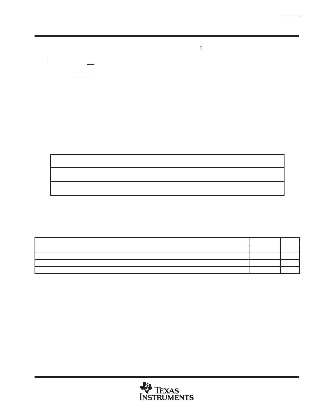
absolute maximum ratings over operating junction temperature range
(unless otherwise noted)
Input voltage range‡, VI –0.3 V to 5.5 V. . . . . . . . . . . . . . . . . . . . . . . . . . . . . . . . . . . . . . . . . . . . . . . . . . . . . . . . . . . .
Voltage range at EN –0.3 V to 16.5 V. . . . . . . . . . . . . . . . . . . . . . . . . . . . . . . . . . . . . . . . . . . . . . . . . . . . . . . . . . . . . .
Maximum PG voltage (TPS751xxQ) 16.5 V. . . . . . . . . . . . . . . . . . . . . . . . . . . . . . . . . . . . . . . . . . . . . . . . . . . . . . . .
Maximum RESET
Peak output current Internally limited. . . . . . . . . . . . . . . . . . . . . . . . . . . . . . . . . . . . . . . . . . . . . . . . . . . . . . . . . . . . . .
Continuous total power dissipation See dissipation rating tables. . . . . . . . . . . . . . . . . . . . . . . . . . . . . . . . . . . . . .
Output voltage, VO (OUTPUT, FB) 5.5 V. . . . . . . . . . . . . . . . . . . . . . . . . . . . . . . . . . . . . . . . . . . . . . . . . . . . . . . . . .
Operating virtual junction temperature range, TJ –40°C to 125°C. . . . . . . . . . . . . . . . . . . . . . . . . . . . . . . . . . . . .
Storage temperature range, T
ESD rating, HBM 2 kV. . . . . . . . . . . . . . . . . . . . . . . . . . . . . . . . . . . . . . . . . . . . . . . . . . . . . . . . . . . . . . . . . . . . . . . . . .
†
Stresses beyond those listed under “absolute maximum ratings” may cause permanent damage to the device. These are stress ratings only, and
functional operation of the device at these or any other conditions beyond those indicated under “recommended operating conditions” is not
implied. Exposure to absolute-maximum-rated conditions for extended periods may affect device reliability.
‡
All voltage values are with respect to network terminal ground.
PACKAGE
§
This parameter is measured with the recommended copper heat sink pattern on a 1-layer PCB, 5-in × 5-in PCB, 1 oz. copper,
2-in × 2-in coverage (4 in2).
¶
This parameter is measured with the recommended copper heat sink pattern on a 8-layer PCB, 1.5-in × 2-in PCB, 1 oz. copper
with layers 1, 2, 4, 5, 7, and 8 at 5% coverage (0.9 in2) and layers 3 and 6 at 100% coverage (6 in2). For more information, refer
to TI technical brief SLMA002.
voltage (TPS753xxQ) 16.5 V. . . . . . . . . . . . . . . . . . . . . . . . . . . . . . . . . . . . . . . . . . . . . . . . . . . .
–65°C to 150°C. . . . . . . . . . . . . . . . . . . . . . . . . . . . . . . . . . . . . . . . . . . . . . . . . . .
stg
DISSIPATION RATING TABLE 1 – FREE-AIR TEMPERATURES
AIR FLOW
(CFM)
0 2.9 W 23.5 mW/°C 1.9 W 1.5 W
300 4.3 W 34.6 mW/°C 2.8 W 2.2 W
0 3 W 23.8 mW/°C 1.9 W 1.5 W
300 7.2 W 57.9 mW/°C 4.6 W 3.8 W
TA < 25°C
POWER RATING
DERATING FACTOR
ABOVE TA = 25°C
Ĕ
TA = 70°C
POWER RATING
TA = 85°C
POWER RATING
recommended operating conditions
MIN MAX UNIT
Input voltage, V
Output voltage range, V
Output current, IO (see Note 1) 0 1.5 A
Operating virtual junction temperature, TJ (see Note 1) –40 125 °C
#
To calculate the minimum input voltage for your maximum output current, use the following equation: V
#
I
O
= V
I(min)
2.7 5 V
1.5 5 V
+ V
O(max)
DO(max load)
.
POST OFFICE BOX 655303 • DALLAS, TEXAS 75265
7
TPS75101Q, TPS75115Q, TPS75118Q, TPS75125Q, TPS75133Q WITH POWER GOOD
j
1.5 V Output
g
1.8 V Output
V
2.5 V Output
3.3 V Output
Quiescent current (GND current) (see Note 2)
A
(
)
()
%/V
Standby current
PG
TPS75301Q, TPS75315Q, TPS75318Q, TPS75325Q, TPS75333Q WITH RESET
FAST-TRANSIENT-RESPONSE 1.5-A LOW-DROPOUT VOLTAGE REGULATORS
SLVS241 – MARCH 2000
electrical characteristics over recommended operating junction temperature range (TJ = –40°C to
125°C), V
Output voltage
(see Notes 1 and 3)
Output voltage line regulation (∆VO/V
see Notes 1 and 2
Output voltage line regulation (∆VO/V
(see Notes 1 and 2)
Load regulation (see Note 3) 1 mV
Output noise voltage
Output current Limit VO = 0 V 3.3 4.5 A
Thermal shutdown junction temperature 150 °C
FB input current TPS75x01Q FB = 1.5 V –1 1 µA
High level enable input voltage 2 V
Low level enable input voltage 0.7 V
Power supply ripple rejection (see Note 2)
PG
(TPS751xxQ)
NOTES: 1. Minimum IN operating voltage is 2.7 V or V
= V
I
PARAMETER TEST CONDITIONS MIN TYP MAX UNIT
Minimum input voltage for valid
PG
Trip threshold voltage VO decreasing 80 86 %V
Hysteresis voltage Measured at V
Output low voltage VI = 2.7 V, I
Leakage current V
2. If VO
+ 1 V, I
O(typ)
≤ 1.8 V then V
= 1 mA, EN = 0 V, CO = 47 µF (unless otherwise noted)
O
Adjustable
Voltage
O
)
O
)
= 2.7 V, V
imin
Line Reg. (mV)
1.5 V ≤ VO ≤ 5 V, TJ = 25°C V
1.5 V ≤ VO ≤ 5 V 0.98 V
TJ = 25°C, 2.7 V < VIN < 5 V 1.5
p
2.7 V < VIN < 5 V 1.470 1.530
TJ = 25°C, 2.8 V < VIN < 5 V 1.8
p
2.8 V < VIN < 5 V 1.764 1.836
TJ = 25°C, 3.5 V < VIN < 5 V 2.5
p
3.5 V < VIN < 5 V 2.450 2.550
TJ = 25°C, 4.3 V < VIN < 5 V 3.3
p
4.3 V < VIN < 5 V 3.234 3.366
TJ = 25°C, See Note 3 75
See Note 3 125
VO + 1 V < VI ≤ 5 V, TJ = 25°C 0.01
VO + 1 V < VI < 5 V 0.1
BW = 300 Hz to 50 kHz, VO = 1.5 V
CO = 100 µF, TJ = 25°C
EN = V
I,
EN = V
I
f = 100 Hz, CO = 100 µF,
TJ = 25°C, See Note 1, IO = 1.5 A
I
= 300µA, V
O(PG)
O
= 5 V 1 µA
(PG)
+ 1 V, whichever is greater. Maximum IN voltage 5 V .
O(typ)
= 5 V:
imax
+ǒ%ńVǓ
TJ = 25°C, 1 µA
≤ 0.8 V 1 1.3 V
(PG)
= 1mA 0.15 0.4 V
O(PG)
ǒ
V
imax
*
V
O
100
2.7 V
Ǔ
1000
O
O
60 µVrms
63 dB
0.5 %V
1.02 V
O
µ
10 µA
O
O
If V
≥ 2.5 V then V
O
3. IO = 1 mA to 1.5 A
8
= VO + 1 V, V
imin
Line Reg. (mV)
POST OFFICE BOX 655303 • DALLAS, TEXAS 75265
= 5 V:
imax
+ǒ%ńVǓ
ǒ
V
imax
*ǒVO)
V
O
100
1V
Ǔ
Ǔ
1000
Input current (EN)
g,( )( )
VOOutput voltage
VDODropout voltage
TPS75101Q, TPS75115Q, TPS75118Q, TPS75125Q, TPS75133Q WITH POWER GOOD
TPS75301Q, TPS75315Q, TPS75318Q, TPS75325Q, TPS75333Q WITH RESET
FAST-TRANSIENT-RESPONSE 1.5-A LOW-DROPOUT VOLTAGE REGULATORS
SLVS241 – MARCH 2000
electrical characteristics over recommended operating junction temperature range (TJ = –40°C to
125°C), V
Reset
(TPS753xxQ)
p
High level EN input voltage 2 V
Low level EN input voltage 0.7 V
Dropout voltage, (3.3 V output) (see Note 4)
NOTE 4: IN voltage equals VO(Typ) – 100 mV; TPS75x15Q, TPS75x18Q and TPS75x25Q dropout voltage limited by input voltage range
= V
I
Minimum input voltage for valid RESET I
Trip threshold voltage VO decreasing 92 98 %V
Hysteresis voltage Measured at V
Output low voltage I
Leakage current V
RESET time-out delay 100 ms
limitations (i.e., TPS75x33Q input voltage needs to drop to 3.2 V for purpose of this test).
+ 1 V, I
O(typ)
PARAMETER TEST CONDITIONS
= 1 mA, EN = 0 V, CO = 47 µF (unless otherwise noted) (continued)
O
O(RESET)
O(RESET)
(RESET)
EN = V
EN = 0 V –1 0 1 µA
IO = 1.5 A,
TJ = 25°C
IO = 1.5 A, VI = 3.2 V 300
= 300 µA, V
O
= 1 mA 0.15 0.4 V
= 5.5 V 1 µA
I
(RESET)
VI = 3.2 V,
MIN TYP MAX UNIT
≤ 0.8 V 1.1 1.3 V
0.5 %V
–1 1 µA
160
O
O
mV
Table of Graphs
FIGURE
p
Ground current vs Junction temperature 6
Power supply ripple rejection vs Frequency 7
Output spectral noise density vs Frequency 8
Z
o
V
O
Output impedance vs Frequency 9
p
Line transient response 12, 14
Load transient response 13, 15
Output voltage vs Time 16
Equivalent series resistance (ESR) vs Output current 18, 19
vs Output current 2, 3
vs Junction temperature 4, 5
vs Input voltage 10
vs Junction temperature 11
POST OFFICE BOX 655303 • DALLAS, TEXAS 75265
9

TPS75101Q, TPS75115Q, TPS75118Q, TPS75125Q, TPS75133Q WITH POWER GOOD
TPS75301Q, TPS75315Q, TPS75318Q, TPS75325Q, TPS75333Q WITH RESET
FAST-TRANSIENT-RESPONSE 1.5-A LOW-DROPOUT VOLTAGE REGULATORS
SLVS241 – MARCH 2000
TYPICAL CHARACTERISTICS
3.305
3.303
3.301
3.299
– Output Voltage – V
O
V
3.297
3.295
0
VI = 4.3 V
TJ = 25°C
TPS75x33Q
OUTPUT VOLTAGE
vs
OUTPUT CURRENT
V
O
500 1500
IO – Output Current – mA
1000
Figure 2
1.503
1.502
1.501
1.5
1.499
– Output Voltage – V
O
V
1.498
1.497
VI = 2.7 V
TJ = 25°C
0
TPS75x15Q
OUTPUT VOLTAGE
vs
OUTPUT CURRENT
V
O
500 15001000
IO – Output Current – mA
Figure 3
3.37
3.35
3.33
3.31
3.29
– Output Voltage – V
O
3.27
V
3.25
3.23
–40 10
TPS75x33Q
OUTPUT VOLTAGE
vs
JUNCTION TEMPERATURE
VI = 4.3 V
1 mA
60 110
TJ – Junction Temperature – °C
Figure 4
1.5 A
160
1.53
1.52
1.51
1.50
1.49
– Output Voltage – V
O
V
1.48
1.47
–40 10
TPS75x15Q
OUTPUT VOLTAGE
vs
JUNCTION TEMPERATURE
VI = 2.7 V
1 mA
1.5 A
11060 160
TJ – Junction Temperature – °C
Figure 5
10
POST OFFICE BOX 655303 • DALLAS, TEXAS 75265

TPS75101Q, TPS75115Q, TPS75118Q, TPS75125Q, TPS75133Q WITH POWER GOOD
TPS75301Q, TPS75315Q, TPS75318Q, TPS75325Q, TPS75333Q WITH RESET
FAST-TRANSIENT-RESPONSE 1.5-A LOW-DROPOUT VOLTAGE REGULATORS
SLVS241 – MARCH 2000
TYPICAL CHARACTERISTICS
TPS75xxxQ
GROUND CURRENT
vs
POWER SUPPLY RIPPLE REJECTION
JUNCTION TEMPERATURE
90
VI = 5 V
IO = 1.5 A
85
80
75
70
65
Ground Current – Aµ
60
55
50
10 11060–40 160
TJ – Junction Temperature – °C
100
90
80
70
60
50
40
30
20
10
PSRR – Power Supply Ripple Rejection – dB
0
VI = 4.3 V
CO = 100 µF
IO = 1.5 A
TJ = 25°C
Figure 6
TPS75x33Q
vs
FREQUENCY
VI = 4.3 V
CO = 100 µF
IO = 1 mA
TJ = 25°C
1k10010
f – Frequency – Hz
100k10k
Figure 7
1M
10M
TPS75x33Q
OUTPUT SPECTRAL NOISE DENSITY
vs
FREQUENCY
2
VI = 4.3 V
1.8
VO = 3.3 V
CO = 100 µF
1.6
TJ = 25°C
1.4
nV/ Hz– Voltage Noise –V
1.2
1
0.8
0.6
n
0.4
0.2
0
1010 100 1k 10k 50k
IO = 1 mA
f – Frequency – Hz
IO = 1.5 A
Figure 8
TPS75x33Q
OUTPUT IMPEDANCE
vs
1
10
Ω
1
–1
10
– Output Impedance –Z
o
–2
10
10 100 100K 1M
FREQUENCY
CO = 100 µF
IO = 1 mA
CO = 100 µF
IO = 1.5 A
10K1K 10M
f – Frequency – Hz
Figure 9
POST OFFICE BOX 655303 • DALLAS, TEXAS 75265
11

TPS75101Q, TPS75115Q, TPS75118Q, TPS75125Q, TPS75133Q WITH POWER GOOD
TPS75301Q, TPS75315Q, TPS75318Q, TPS75325Q, TPS75333Q WITH RESET
FAST-TRANSIENT-RESPONSE 1.5-A LOW-DROPOUT VOLTAGE REGULATORS
SLVS241 – MARCH 2000
TYPICAL CHARACTERISTICS
300
250
200
150
100
– Dropout Voltage – mV
DO
V
50
0
TPS75x01Q
DROPOUT VOLTAGE
vs
INPUT VOLTAGE
IO = 1.5 A
TJ = 125°C
TJ = 25°C
TJ = –40°C
34
3.52.5
VI – Input Voltage – V
Figure 10
4.5 5
300
JUNCTION TEMPERATURE
250
200
150
100
– Dropout Voltage – mV
DO
V
50
0
–40 10 11060
TJ – Junction Temperature – °C
TPS75x33Q
DROPOUT VOLTAGE
vs
IO = 1.5 A
IO = 0.5 A
160
Figure 11
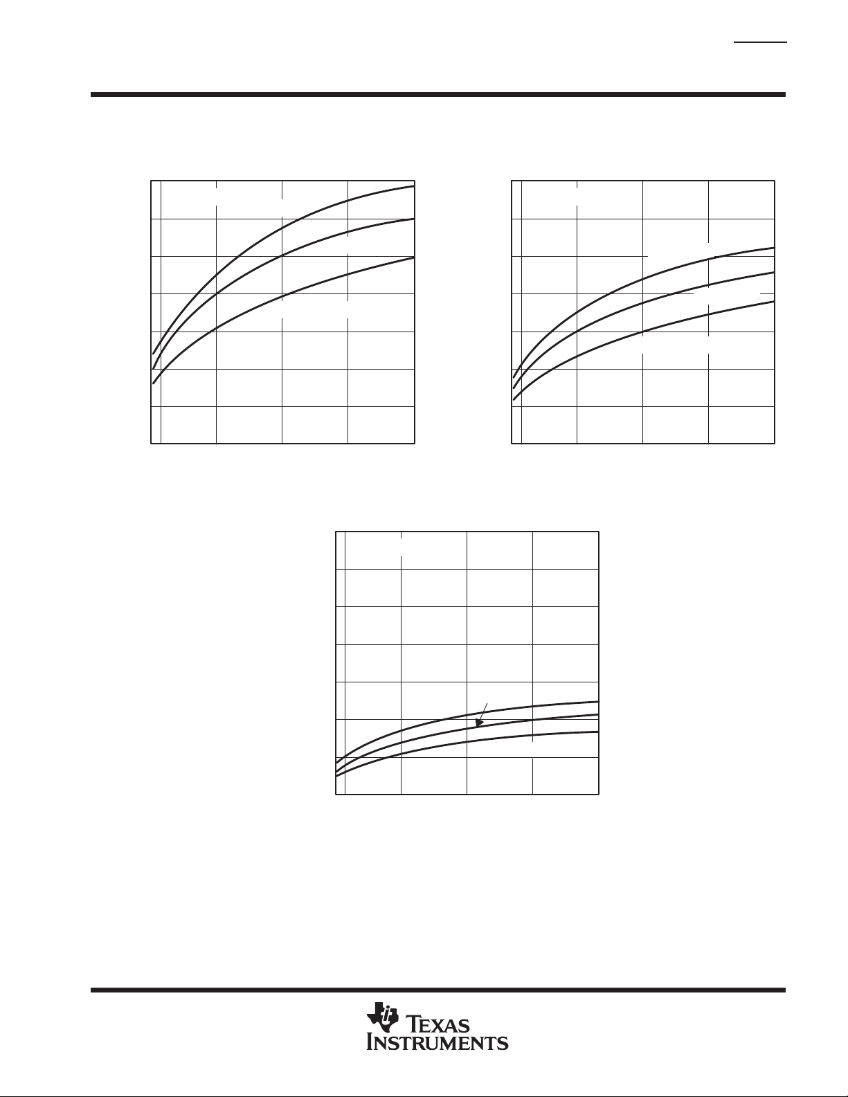
TPS75x15Q
LINE TRANSIENT RESPONSE
IO=1.5 A
CO=100 µF
VO=1.5 V
100
– Change in
O
0
V
∆
Output Voltage – mV
–100
4
3
– Input Voltage – V
I
V
0 0.30.20.1 0.4 0.5 0.70.6 0.8 0.9 1
t – Time – ms
Figure 12
dv
dt
+
1V
µs
50
– Change in∆
O
–50
V
Output Voltage – mV
–100
–150
1.5
O
I – Output Current – A
TPS75x15Q
LOAD TRANSIENT RESPONSE
IL=1.5 A
CL=100 µF (T antalum)
VO=1.5 V
0
0
032145768910
t – Time – ms
Figure 13
12
POST OFFICE BOX 655303 • DALLAS, TEXAS 75265

TPS75101Q, TPS75115Q, TPS75118Q, TPS75125Q, TPS75133Q WITH POWER GOOD
TPS75301Q, TPS75315Q, TPS75318Q, TPS75325Q, TPS75333Q WITH RESET
FAST-TRANSIENT-RESPONSE 1.5-A LOW-DROPOUT VOLTAGE REGULATORS
SLVS241 – MARCH 2000
TYPICAL CHARACTERISTICS
100
– Change in
O
0
V
∆
Output Voltage – mV
–100
5.3
4.3
– Input Voltage – V
I
V
TPS75x33Q
LINE TRANSIENT RESPONSE
IO=1.5 A
CO=100 µF (T antalum)
VO=3.3 V
0.30.20.1 0.4 0.5 0.70.6 0.8 0.9 10
t – Time – ms
Figure 14
dv
1V
+
µs
dt
TPS75x33Q
OUTPUT VOLTAGE
vs
TIME (STARTUP)
50
0
– Change in∆
O
V
–50
Output Voltage – mV
–100
–150
1.5
O
I – Output Current – A
TPS75x33Q
LOAD TRANSIENT RESPONSE
IO=1.5 A
CO=100 µF (T antalum)
VO=3.3 V
0
321457689100
t – Time – ms
Figure 15
3.3
– Output Voltage – V
O
V
0
4.3
0
Enable Voltage – V
0
VI = 4.3 V
TJ = 25°C
0.2 10.4 0.6 0.8
t – Time – ms
Figure 16
POST OFFICE BOX 655303 • DALLAS, TEXAS 75265
13

TPS75101Q, TPS75115Q, TPS75118Q, TPS75125Q, TPS75133Q WITH POWER GOOD
TPS75301Q, TPS75315Q, TPS75318Q, TPS75325Q, TPS75333Q WITH RESET
FAST-TRANSIENT-RESPONSE 1.5-A LOW-DROPOUT VOLTAGE REGULATORS
SLVS241 – MARCH 2000
TYPICAL CHARACTERISTICS
+
C
ESR
To Load
O
R
L
V
I
IN
EN
OUT
GND
Figure 17. Test Circuit for Typical Regions of Stability (Figures 18 and 19) (Fixed Output Options)
TYPICAL REGION OF STABILITY
EQUIVALENT SERIES RESISTANCE
vs
OUTPUT CURRENT
10
Vo = 3.3 V
Co = 100 µF
VI = 4.3 V
TJ = 25°C
1
Region of Stability
†
10
1
TYPICAL REGION OF STABILITY
EQUIVALENT SERIES RESISTANCE
vs
OUTPUT CURRENT
Vo = 3.3 V
Co = 47 µF
VI = 4.3 V
TJ = 25°C
Region of Stability
†
0.1
0.05
ESR – Equivalent series restance – Ω
Region of Instability
0.01
0 0.5 1 1.5
IO – Output Current – A
Figure 18
†
Equivalent series resistance (ESR) refers to the total series resistance, including the ESR of the capacitor, any series resistance added externally ,
and PWB trace resistance to CO.
0.1
ESR – Equivalent series restance – Ω
Region of Instability
0.01
0 0.5 1 1.5
IO – Output Current – A
Figure 19
14
POST OFFICE BOX 655303 • DALLAS, TEXAS 75265

TPS75101Q, TPS75115Q, TPS75118Q, TPS75125Q, TPS75133Q WITH POWER GOOD
TPS75301Q, TPS75315Q, TPS75318Q, TPS75325Q, TPS75333Q WITH RESET
FAST-TRANSIENT-RESPONSE 1.5-A LOW-DROPOUT VOLTAGE REGULATORS
SLVS241 – MARCH 2000
APPLICATION INFORMATION
The TPS751xxQ or TPS753xxQ family includes four fixed-output voltage regulators (1.5 V , 1.8 V , 2.5 V and 3.3
V), and an adjustable regulator, the TPS75x01Q (adjustable from 1.5 V to 5 V).
minimum load requirements
The TPS751xxQ and TPS753xxQ families are stable even at no load; no minimum load is required for operation.
pin functions
enable (EN)
The EN
shutdown mode. When EN goes to logic low, then the device will be enabled.
power-good (PG) (TPS751xxQ)
The PG terminal is an open drain, active high output that indicates the status of VO (output of the LDO). When
V
state when VO falls below 83% (i.e. over load condition) of the regulated voltage. The open drain output of the
PG terminal requires a pullup resistor
sense (SENSE)
The SENSE terminal of the fixed-output options must be connected to the regulator output, and the connection
should be as short as possible. Internally, SENSE connects to a high-impedance wide-bandwidth amplifier
through a resistor-divider network and noise pickup feeds through to the regulator output. It is essential to route
the SENSE connection in such a way to minimize/avoid noise pickup. Adding RC networks between the SENSE
terminal and V
feedback (FB)
FB is an input terminal used for the adjustable-output options and must be connected to an external feedback
resistor divider. The FB connection should be as short as possible. It is essential to route it in such a way to
minimize/avoid noise pickup. Adding RC networks between FB terminal and VO to filter noise is not
recommended because it may cause the regulator to oscillate.
reset (RESET
The RESET terminal is an open drain, active low output that indicates the status of VO. When VO reaches 95%
of the regulated voltage, RESET will go to a low-impedance state after a 100-ms delay. RESET will go to a
high-impedance state when VO is below 95% of the regulated voltage. The open-drain output of the RESET
terminal requires a pullup resistor.
terminal is an input which enables or shuts down the device. If EN is a logic high, the device will be in
reaches 83% of the regulated voltage, PG will go to a high impedance state. It will go to a low-impedance
O
.
to filter noise is not recommended because it may cause the regulator to oscillate.
O
) (TPS753xxQ)
GND/HEATSINK
All GND/HEA TSINK terminals are connected directly to the mount pad for thermal-enhanced operation. These
terminals could be connected to GND or left floating.
input capacitor
For a typical application, an input bypass capacitor (0.22 µF – 1 µF) is recommended for device stability . This
capacitor should be as close to the input pins as possible. For fast transient condition where droop at the input
of the LDO may occur due to high inrush current, it is recommended to place a larger capacitor at the input as
well. The size of this capacitor is dependant on the output current and response time of the main power supply ,
as well as the distance to the load (LDO).
POST OFFICE BOX 655303 • DALLAS, TEXAS 75265
15

TPS75101Q, TPS75115Q, TPS75118Q, TPS75125Q, TPS75133Q WITH POWER GOOD
TPS75301Q, TPS75315Q, TPS75318Q, TPS75325Q, TPS75333Q WITH RESET
FAST-TRANSIENT-RESPONSE 1.5-A LOW-DROPOUT VOLTAGE REGULATORS
SLVS241 – MARCH 2000
APPLICATION INFORMATION
output capacitor
As with most LDO regulators, the TPS751xxQ and TPS753xxQ require an output capacitor connected between
OUT and GND to stabilize the internal control loop. The minimum recommended capacitance value is 47 µF
and the ESR (equivalent series resistance) must be between 100 mΩ and 10 Ω. Solid tantalum electrolytic,
aluminum electrolytic, and multilayer ceramic capacitors are all suitable, provided they meet the requirements
described in this section. Larger capacitors provide a wider range of stability and better load transient response.
This information, along with the ESR graphs, is included to assist in selection of suitable capacitance for the
user’s application. When necessary to achieve low height requirements along with high output current and/or
high load capacitance, several higher ESR capacitors can be used in parallel to meet these guidelines.
ESR and transient response
LDOs typically require an external output capacitor for stability. In fast transient response applications,
capacitors are used to support the load current while LDO amplifier is responding. In most applications, one
capacitor is used to support both functions.
Besides its capacitance, every capacitor also contains parasitic impedances. These parasitic impedances are
resistive as well as inductive. The resistive impedance is called equivalent series resistance (ESR), and the
inductive impedance is called equivalent series inductance (ESL). The equivalent schematic diagram of any
capacitor can therefore be drawn as shown in Figure 20.
R
ESR
Figure 20. – ESR and ESL
L
ESL
C
16
POST OFFICE BOX 655303 • DALLAS, TEXAS 75265

TPS75101Q, TPS75115Q, TPS75118Q, TPS75125Q, TPS75133Q WITH POWER GOOD
TPS75301Q, TPS75315Q, TPS75318Q, TPS75325Q, TPS75333Q WITH RESET
FAST-TRANSIENT-RESPONSE 1.5-A LOW-DROPOUT VOLTAGE REGULATORS
SLVS241 – MARCH 2000
APPLICATION INFORMATION
In most cases one can neglect the effect of inductive impedance ESL. Therefore, the following application
focuses mainly on the parasitic resistance ESR.
Figure 21 shows the output capacitor and its parasitic impedances in a typical LDO output stage.
I
O
LDO
+
V
ESR
V
I
R
ESR
–
R
LOAD
C
O
V
O
Figure 21. LDO Output Stage With Parasitic Resistances ESR and ESL
In steady state (dc state condition), the load current is supplied by the LDO (solid arrow) and the voltage across
the capacitor is the same as the output voltage (V(CO) = VO). This means no current is flowing into the C
branch. If IO suddenly increases (transient condition), the following occurs:
D
The LDO is not able to supply the sudden current need due to its response time (t1 in Figure 22). Therefore,
capacitor C
provides the current for the new load condition (dashed arrow). CO now acts like a battery with
O
an internal resistance, ESR. Depending on the current demand at the output, a voltage drop will occur at
R
. This voltage is shown as V
ESR
D
When CO is conducting current to the load, initial voltage at the load will be VO = V(CO) – V
in Figure 21.
ESR
. Due to the
ESR
discharge of CO, the output voltage VO will drop continuously until the response time t1 of the LDO is reached
and the LDO will resume supplying the load. From this point, the output voltage starts rising again until it
reaches the regulated voltage. This period is shown as t2 in Figure 22.
Figure 22 also shows the impact of different ESRs on the output voltage. The left brackets show different levels
of ESRs where number 1 displays the lowest and number 3 displays the highest ESR.
From above, the following conclusions can be drawn:
D
The higher the ESR, the larger the droop at the beginning of load transient.
D
The smaller the output capacitor, the faster the discharge time and the bigger the voltage droop during the
LDO response period.
O
POST OFFICE BOX 655303 • DALLAS, TEXAS 75265
17

TPS75101Q, TPS75115Q, TPS75118Q, TPS75125Q, TPS75133Q WITH POWER GOOD
TPS75301Q, TPS75315Q, TPS75318Q, TPS75325Q, TPS75333Q WITH RESET
FAST-TRANSIENT-RESPONSE 1.5-A LOW-DROPOUT VOLTAGE REGULATORS
SLVS241 – MARCH 2000
APPLICATION INFORMATION
conclusion
To minimize the transient output droop, capacitors must have a low ESR and be large enough to support the
minimum output voltage requirement.
I
O
V
O
1
2
3
ESR 1
ESR 2
ESR 3
t
1
t
2
Figure 22. Correlation of Different ESRs and Their Influence to the Regulation of VO at a
Load Step From Low-to-High Output Current
18
POST OFFICE BOX 655303 • DALLAS, TEXAS 75265
TPS75101Q, TPS75115Q, TPS75118Q, TPS75125Q, TPS75133Q WITH POWER GOOD
TPS75301Q, TPS75315Q, TPS75318Q, TPS75325Q, TPS75333Q WITH RESET
FAST-TRANSIENT-RESPONSE 1.5-A LOW-DROPOUT VOLTAGE REGULATORS
SLVS241 – MARCH 2000
APPLICATION INFORMATION
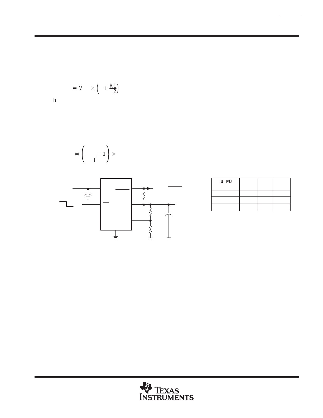
programming the TPS75x01Q adjustable LDO regulator
The output voltage of the TPS75x01Q adjustable regulator is programmed using an external resistor divider as
shown in Figure 23. The output voltage is calculated using:
R1
VO+
V
ǒ1
ref
Where:
V
= 1.1834 V typ (the internal reference voltage)
ref
Resistors R1 and R2 should be chosen for approximately 40-µA divider current. Lower value resistors can be
used but offer no inherent advantage and waste more power. Higher values should be avoided as leakage
currents at FB increase the output voltage error. The recommended design procedure is to choose
R2 = 30.1 kΩ to set the divider current at 40 µA and then calculate R1 using:
V
+ ǒ
O
*
V
ref
≥ 2 V
R1
V
I
0.22 µF
≤ 0.7 V
Ǔ
)
R2
1
Ǔ
R2
TPS75x01Q
PG or
IN
RESET
EN
FB/SENSE
GND
OUT
PG or RESET
250 kΩ
R1
R2
V
C
O
Output
O
OUTPUT VOLTAGE
PROGRAMMING GUIDE
OUTPUT
VOLTAGE
2.5 V
3.3 V
3.6 V
NOTE: To reduce noise and prevent
oscillation, R1 and R2 need to be as close
as possible to the FB/SENSE terminal.
R1 R2
30.1
33.2
30.1
53.6
30.1
61.9
(1)
(2)
UNIT
kΩ
kΩ
kΩ
Figure 23. TPS75x01Q Adjustable LDO Regulator Programming
POST OFFICE BOX 655303 • DALLAS, TEXAS 75265
19
TPS75101Q, TPS75115Q, TPS75118Q, TPS75125Q, TPS75133Q WITH POWER GOOD
TPS75301Q, TPS75315Q, TPS75318Q, TPS75325Q, TPS75333Q WITH RESET
FAST-TRANSIENT-RESPONSE 1.5-A LOW-DROPOUT VOLTAGE REGULATORS
SLVS241 – MARCH 2000
APPLICATION INFORMATION
regulator protection
The TPS751xxQ or TPS753xxQ PMOS-pass transistor has a built-in back diode that conducts reverse currents
when the input voltage drops below the output voltage (e.g., during power down). Current is conducted from
the output to the input and is not internally limited. When extended reverse voltage is anticipated, external
limiting may be appropriate.
The TPS751xxQ or TPS753xxQ also features internal current limiting and thermal protection. During normal
operation, the TPS751xxQ or TPS753xxQ limits output current to approximately 3.3 A. When current limiting
engages, the output voltage scales back linearly until the overcurrent condition ends. While current limiting is
designed to prevent gross device failure, care should be taken not to exceed the power dissipation ratings of
the package. If the temperature of the device exceeds 150°C(typ), thermal-protection circuitry shuts it down.
Once the device has cooled below 130°C(typ), regulator operation resumes.
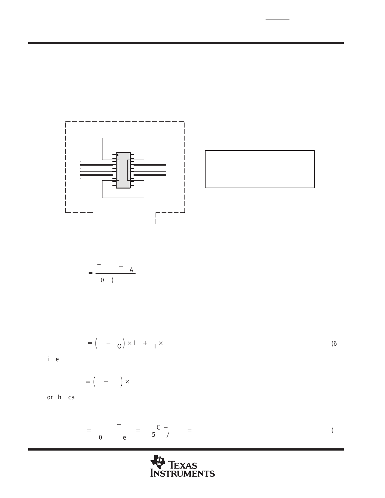
power dissipation and junction temperature
Specified regulator operation is assured to a junction temperature of 125°C; the maximum junction temperature
should be restricted to 125°C under normal operating conditions. This restriction limits the power dissipation
the regulator can handle in any given application. T o ensure the junction temperature is within acceptable limits,
calculate the maximum allowable dissipation, P
or equal to P
The maximum-power-dissipation limit is determined using the following equation:
D(max)
.
, and the actual dissipation, PD, which must be less than
D(max)
P
D(max)
Where:
TJmax is the maximum allowable junction temperature
R
is the thermal resistance junction-to-ambient for the package, i.e., 34.6°C/W for the 20-terminal
θJA
PWP with no airflow (see Table 1).
T
is the ambient temperature.
A
The regulator dissipation is calculated using:
PD+ǒVI*
Power dissipation resulting from quiescent current is negligible. Excessive power dissipation will trigger the
thermal protection circuit.
TJmax*T
+
V
O
R
Ǔ
A
q
JA
I
O
(3)
(4)
20
POST OFFICE BOX 655303 • DALLAS, TEXAS 75265
TPS75101Q, TPS75115Q, TPS75118Q, TPS75125Q, TPS75133Q WITH POWER GOOD
TPS75301Q, TPS75315Q, TPS75318Q, TPS75325Q, TPS75333Q WITH RESET
FAST-TRANSIENT-RESPONSE 1.5-A LOW-DROPOUT VOLTAGE REGULATORS
SLVS241 – MARCH 2000
THERMAL INFORMATION
thermally enhanced TSSOP-20 (PWP – PowerPad)
The thermally enhanced PWP package is based on the 20-pin TSSOP, but includes a thermal pad [see
Figure 24(c)] to provide an effective thermal contact between the IC and the PWB.
Traditionally, surface mount and power have been mutually exclusive terms. A variety of scaled-down
TO220-type packages have leads formed as gull wings to make them applicable for surface-mount applications.
These packages, however, suffer from several shortcomings: they do not address the very low profile
requirements (<2 mm) of many of today’s advanced systems, and they do not offer a pin-count high enough
to accommodate increasing integration. On the other hand, traditional low-power surface-mount packages
require power-dissipation derating that severely limits the usable range of many high-performance analog
circuits.
The PWP package (thermally enhanced TSSOP) combines fine-pitch surface-mount technology with thermal
performance comparable to much larger power packages.
The PWP package is designed to optimize the heat transfer to the PWB. Because of the very small size and
limited mass of a TSSOP package, thermal enhancement is achieved by improving the thermal conduction
paths that remove heat from the component. The thermal pad is formed using a lead-frame design (patent
pending) and manufacturing technique to provide the user with direct connection to the heat-generating IC.
When this pad is soldered or otherwise coupled to an external heat dissipator, high power dissipation in the
ultrathin, fine-pitch, surface-mount package can be reliably achieved.
DIE
Side View (a)
DIE
End View (b)
Thermal
Pad
Bottom View (c)
Figure 24. Views of Thermally Enhanced PWP Package
Because the conduction path has been enhanced, power-dissipation capability is determined by the thermal
considerations in the PWB design. For example, simply adding a localized copper plane (heat-sink surface),
which is coupled to the thermal pad, enables the PWP package to dissipate 2.5 W in free air (reference
Figure 26(a), 8 cm2 of copper heat sink and natural convection). Increasing the heat-sink size increases the
power dissipation range for the component. The power dissipation limit can be further improved by adding
airflow to a PWB/IC assembly (see Figures 25 and 26). The line drawn at 0.3 cm
2
in Figures 25 and 26 indicates
performance at the minimum recommended heat-sink size, illustrated in Figure 28.
POST OFFICE BOX 655303 • DALLAS, TEXAS 75265
21
TPS75101Q, TPS75115Q, TPS75118Q, TPS75125Q, TPS75133Q WITH POWER GOOD
TPS75301Q, TPS75315Q, TPS75318Q, TPS75325Q, TPS75333Q WITH RESET
FAST-TRANSIENT-RESPONSE 1.5-A LOW-DROPOUT VOLTAGE REGULATORS
SLVS241 – MARCH 2000
THERMAL INFORMATION
thermally enhanced TSSOP-20 (PWP – PowerPad) (continued)
The thermal pad is directly connected to the substrate of the IC, which for the TPS751xxQPWP and
TPS753XXQPWP series is a secondary electrical connection to device ground. The heat-sink surface that is
added to the PWP can be a ground plane or left electrically isolated. In TO220-type surface-mount packages,
the thermal connection is also the primary electrical connection for a given terminal which is not always ground.
The PWP package provides up to 16 independent leads that can be used as inputs and outputs (Note: leads
1, 10, 11, and 20 are internally connected to the thermal pad and the IC substrate).
THERMAL RESISTANCE
vs
COPPER HEAT-SINK AREA
150
125
C/W
°
100
75
– Thermal Resistance –
JA
θ
R
50
25
Natural Convection
50 ft/min
250 ft/min
0235
1460.3
100 ft/min
150 ft/min
200 ft/min
300 ft/min
Copper Heat-Sink Area – cm
Figure 25
78
2
22
POST OFFICE BOX 655303 • DALLAS, TEXAS 75265
TPS75101Q, TPS75115Q, TPS75118Q, TPS75125Q, TPS75133Q WITH POWER GOOD
TPS75301Q, TPS75315Q, TPS75318Q, TPS75325Q, TPS75333Q WITH RESET
FAST-TRANSIENT-RESPONSE 1.5-A LOW-DROPOUT VOLTAGE REGULATORS
THERMAL INFORMATION
thermally enhanced TSSOP-20 (PWP – PowerPad) (continued)
SLVS241 – MARCH 2000
3.5
TA = 25°C
3
2.5
2
1.5
1
– Power Dissipation Limit – W
D
P
0.5
0
0246
0.3
300 ft/min
Natural Convection
Copper Heat-Sink Size – cm
(a)
3.5
150 ft/min
2
TA = 105°C
3
3.5
TA = 55°C
3
2.5
2
1.5
1
– Power Dissipation Limit – W
D
P
0.5
0
8
0246
0.3
Copper Heat-Sink Size – cm
300 ft/min
150 ft/min
Natural Convection
8
2
(b)
2.5
2
1.5
300 ft/min
1
– Power Dissipation Limit – W
D
P
0.5
0
0246
0.3
Copper Heat-Sink Size – cm
150 ft/min
Natural Convection
8
2
(c)
Figure 26. Power Ratings of the PWP Package at Ambient Temperatures of 25°C, 55°C, and 105°C
POST OFFICE BOX 655303 • DALLAS, TEXAS 75265
23
TPS75101Q, TPS75115Q, TPS75118Q, TPS75125Q, TPS75133Q WITH POWER GOOD
TPS75301Q, TPS75315Q, TPS75318Q, TPS75325Q, TPS75333Q WITH RESET
FAST-TRANSIENT-RESPONSE 1.5-A LOW-DROPOUT VOLTAGE REGULATORS
SLVS241 – MARCH 2000
THERMAL INFORMATION
thermally enhanced TSSOP-20 (PWP – PowerPad) (continued)
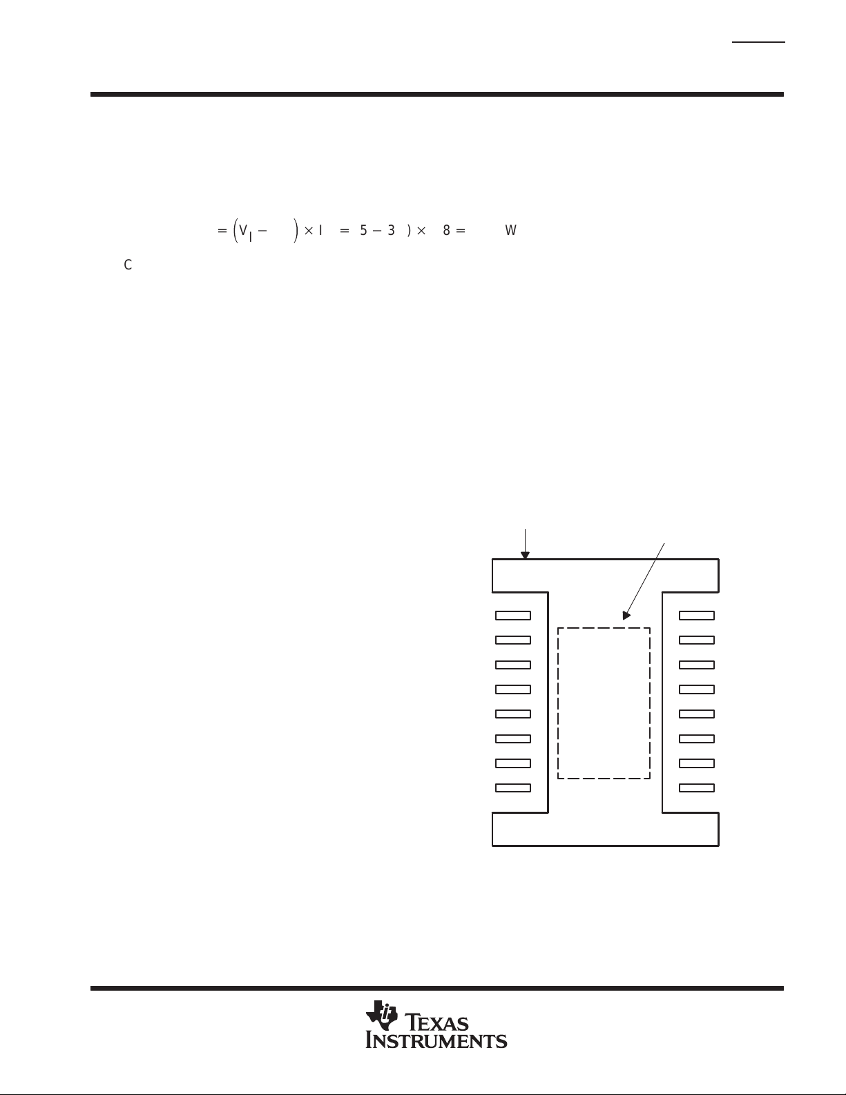
Figure 27 is an example of a thermally enhanced PWB layout for use with the new PWP package. This board
configuration was used in the thermal experiments that generated the power ratings shown in Figure 25 and
Figure 26. As discussed earlier, copper has been added on the PWB to conduct heat away from the device. R
for this assembly is illustrated in Figure 25 as a function of heat-sink area. A family of curves is included to
illustrate the effect of airflow introduced into the system.
Heat-Sink Area
1 oz Copper
Board thickness 62 mils
Board size 3.2 in. × 3.2 in.
Board material FR4
Copper trace/heat sink 1 oz
Exposed pad mounting 63/67 tin/lead solder
θJA
Figure 27. PWB Layout (Including Copper Heatsink Area) for Thermally Enhanced PWP Package
From Figure 25, R
power-dissipation limit for the component/PWB assembly, with the equation:
P
D(max)
Where:
TJmax is the maximum specified junction temperature (150°C absolute maximum limit, 125°C recommended
operating limit) and TA is the ambient temperature.
P
for calculating total internal power dissipation of the TPS75133QPWP is:
Since the quiescent current of the TPS75133QPWP is very low, the second term is negligible, further simplifying
the equation to:
For the case where TA = 55°C, airflow = 200 ft/min, copper heat-sink area = 4 cm2, the maximum
power-dissipation limit can be calculated. First, from Figure 25, we find the system R
the maximum power-dissipation limit is:
should then be applied to the internal power dissipated by the TPS75133QPWP regulator. The equation
D(max)
P
D(total)
P
D(total)
+
+ǒVI*
+ǒVI*
for a PWB assembly can be determined and used to calculate the maximum
θJA
TJmax*T
R
q
JA(system)
A
Ǔ
V
IO)
VI
O
Ǔ
V
I
O
O
I
Q
is 50°C/W; therefore,
θJA
(5)
(6)
(7)
24
P
D(max)
TJmax*T
+
R
q
A
JA(system)
+
POST OFFICE BOX 655303 • DALLAS, TEXAS 75265
°
50 CńW
+
1.4 W
°°
125 C*55 C
(8)
TPS75101Q, TPS75115Q, TPS75118Q, TPS75125Q, TPS75133Q WITH POWER GOOD
TPS75301Q, TPS75315Q, TPS75318Q, TPS75325Q, TPS75333Q WITH RESET
FAST-TRANSIENT-RESPONSE 1.5-A LOW-DROPOUT VOLTAGE REGULATORS
SLVS241 – MARCH 2000
THERMAL INFORMATION
thermally enhanced TSSOP-20 (PWP – PowerPad) (continued)
If the system implements a TPS75133QPWP regulator, where VI = 5 V and IO = 800 mA, the internal power
dissipation is:
P
D(total)
Comparing P
calculated limit. When it does, one of two corrective actions should be made: raising the power-dissipation limit
by increasing the airflow or the heat-sink area, or lowering the internal power dissipation of the regulator by
reducing the input voltage or the load current. In either case, the above calculations should be repeated with
the new system parameters.
+ǒVI*
D(total)
with P
V
O
Ǔ
IO+(5*
reveals that the power dissipation in this example does not exceed the
D(max)
3.3) 0.8+1.36 W
mounting information
The primary requirement is to complete the thermal contact between the thermal pad and the PWB metal. The
thermal pad is a solderable surface and is fully intended to be soldered at the time the component is mounted.
Although voiding in the thermal-pad solder-connection is not desirable, up to 50% voiding is acceptable. The
data included in Figures 25 and 26 is for soldered connections with voiding between 20% and 50%. The thermal
analysis shows no significant difference resulting from the variation in voiding percentage.
Figure 28 shows the solder-mask land pattern for
the PWP package. The minimum recommended
heat-sink area is also illustrated. This is simply a
copper plane under the body extent of the
package, including metal routed under terminals
1, 10, 11, and 20.
Minimum Recommended
Heat-Sink Area
Location of Exposed
Thermal Pad on
PWP Package
(9)
Figure 28. PWP Package Land Pattern
POST OFFICE BOX 655303 • DALLAS, TEXAS 75265
25

TPS75101Q, TPS75115Q, TPS75118Q, TPS75125Q, TPS75133Q WITH POWER GOOD
TPS75301Q, TPS75315Q, TPS75318Q, TPS75325Q, TPS75333Q WITH RESET
FAST-TRANSIENT-RESPONSE 1.5-A LOW-DROPOUT VOLTAGE REGULATORS
SLVS241 – MARCH 2000
MECHANICAL DATA
PWP (R-PDSO-G**) PowerPAD PLASTIC SMALL-OUTLINE PACKAGE
20-PIN SHOWN
0,65
20
1
1,20 MAX
0,30
0,19
11
4,50
4,30
10
A
0,15
0,05
PINS **
DIM
M
0,10
6,60
6,20
Seating Plane
0,10
1614
Thermal Pad
(See Note D)
20
0,15 NOM
0°–8°
Gage Plane
0,25
0,75
0,50
2824
A MAX
A MIN
NOTES: A. All linear dimensions are in millimeters.
B. This drawing is subject to change without notice.
C. Body dimensions do not include mold flash or protrusions.
D. The package thermal performance may be enhanced by bonding the thermal pad to an external thermal plane. This pad is electrically
and thermally connected to the backside of the die and possibly selected leads.
E. Falls within JEDEC MO-153
PowerPAD is a trademark of Texas Instruments.
5,10
4,90
5,10
4,90
6,60
6,40
7,90
7,70
9,80
9,60
4073225/E 03/97
26
POST OFFICE BOX 655303 • DALLAS, TEXAS 75265

IMPORTANT NOTICE
T exas Instruments and its subsidiaries (TI) reserve the right to make changes to their products or to discontinue
any product or service without notice, and advise customers to obtain the latest version of relevant information
to verify, before placing orders, that information being relied on is current and complete. All products are sold
subject to the terms and conditions of sale supplied at the time of order acknowledgment, including those
pertaining to warranty, patent infringement, and limitation of liability.
TI warrants performance of its semiconductor products to the specifications applicable at the time of sale in
accordance with TI’s standard warranty. T esting and other quality control techniques are utilized to the extent
TI deems necessary to support this warranty . Specific testing of all parameters of each device is not necessarily
performed, except those mandated by government requirements.
Customers are responsible for their applications using TI components.
In order to minimize risks associated with the customer’s applications, adequate design and operating
safeguards must be provided by the customer to minimize inherent or procedural hazards.
TI assumes no liability for applications assistance or customer product design. TI does not warrant or represent
that any license, either express or implied, is granted under any patent right, copyright, mask work right, or other
intellectual property right of TI covering or relating to any combination, machine, or process in which such
semiconductor products or services might be or are used. TI’s publication of information regarding any third
party’s products or services does not constitute TI’s approval, warranty or endorsement thereof.
Copyright 2000, Texas Instruments Incorporated
 Loading...