

Page 1
www.ti.com
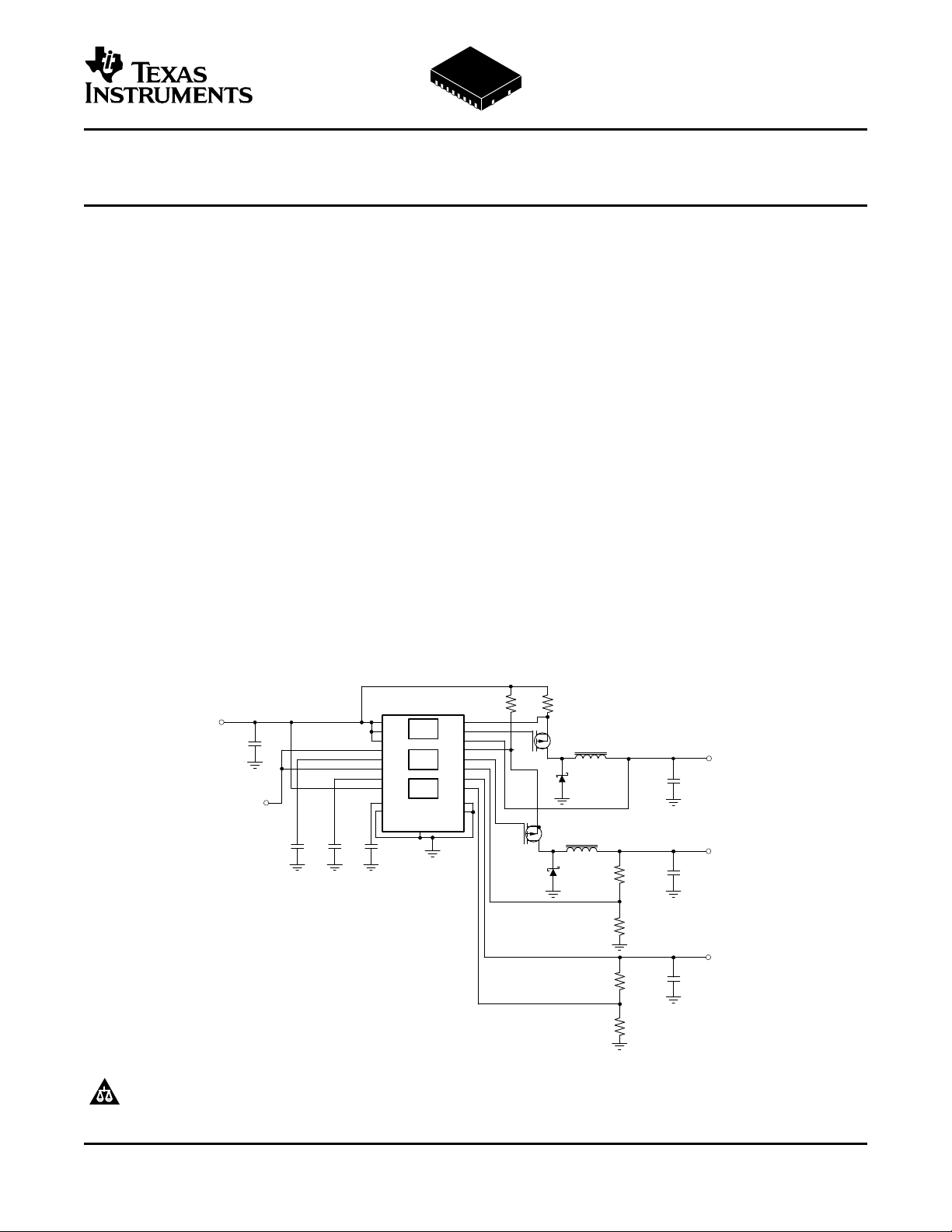
IN1
IN2
IN3
EN1
SS1
EN2
SS2
EN3
IS1
SW 1
FB1
IS2
SW 2
FB2
OUT 3
FB3
DGN D
3A
BUC K1
3A
BUC K2
300mA
LDO
SS3
DGND
AGN D
DGND
TPS75003
+
+
V
CCAUX
2.5V @ 300m A
V
CCO
3.3V @ 3A
V
CCINT
1.2V @ 3A
V
CCAUX
5V_Input
Triple-Supply Power Management IC
for Powering FPGAs and DSPs
FEATURES DESCRIPTION
• Two 95% Efficient, 3A Buck Controllers and
One 300mA LDO
• Tested and Endorsed by Xilinx for Powering
the Spartan™-3, Spartan-3E and Spartan-3L
FPGAs
• Adjustable (1.2V to 6.5V for Bucks, 1.0V to
6.5V for LDO) Output Voltages on All
Channels
• Input Voltage Range: 2.2V to 6.5V
• Independent Soft-Start for Each Supply
• Independent Enable for Each Supply for
Flexible Sequencing
• LDO Stable with 2.2µF Ceramic Output Cap
• Small, Low-Profile 4.5mm x 3.5mm x 0.9mm
QFN Package
APPLICATIONS
• FPGA/DSP/ASIC Supplies
• Set-Top Boxes
• DSL Modems
• Plasma TV Display Panels
TPS75003
SBVS052D – OCTOBER 2004 – REVISED MARCH 2005
The TPS75003 is a complete power management
solution for FPGA, DSP and other multi-supply applications. The device has been tested with and meets
all of the Xilinx Spartan-3, Spartan-3E and
Spartan-3L start-up profile requirements, including
monotonic voltage ramp and minimum voltage rail
rise time. Independent Enables for each output allow
sequencing to minimize demand on the power supply
at start-up. Soft-start on each supply limits inrush
current during start-up. Two integrated buck controllers allow efficient, cost-effective voltage conversion
for both low and high current supplies such as core
and I/O. A 300mA LDO is integrated to provide an
auxiliary rail such as V
FPGA. All three supply voltages are offered in
user-programmable options for maximum flexibility.
The TPS75003 is fully specified from -40 ° C to +85 ° C
and is offered in a QFN package, yielding a highly
compact total solution size with high power dissipation capability.
on the Xilinx Spartan-3
CCAUX
Please be aware that an important notice concerning availability, standard warranty, and use in critical applications of Texas
Instruments semiconductor products and disclaimers thereto appears at the end of this data sheet.
Spartan is a trademark of Xilinx, Inc.
All trademarks are the property of their respective owners.
PRODUCTION DATA information is current as of publication date.
Products conform to specifications per the terms of the Texas
Instruments standard warranty. Production processing does not
necessarily include testing of all parameters.
Copyright © 2004–2005, Texas Instruments Incorporated
Page 2
www.ti.com
TPS75003
SBVS052D – OCTOBER 2004 – REVISED MARCH 2005
This integrated circuit can be damaged by ESD. Texas Instruments recommends that all integrated
circuits be handled with appropriate precautions. Failure to observe proper handling and installation
procedures can cause damage.
ESD damage can range from subtle performance degradation to complete device failure. Precision
integrated circuits may be more susceptible to damage because very small parametric changes could
cause the device not to meet its published specifications.
ORDERING INFORMATION
PRODUCT V
(1)
OUT
Buck1: Adjustable
TPS75003 Buck2: Adjustable
LDO: Adjustable
(1) For the most current specifications and package information, see the Package Option Addendum located at the end of this document, or
see the TI website at www.ti.com .
ABSOLUTE MAXIMUM RATINGS
over operating free-air temperature range (unless otherwise noted)
V
range (IN1, IN2, IN3) -0.3 to +7.0 V
INX
V
range (EN1, EN2, EN3) -0.3 to V
ENX
V
range (SW1, SW2, SW3) -0.3 to V
SWX
V
range (IS1, IS2, IS3) -0.3 to V
ISX
V
range -0.3 to +7.0 V
OUT3
V
range (SS1, SS2, SS3) -0.3 to V
SSX
V
range (FB1, FB2, FB3) -0.3 to +3.3 V
FBX
Peak LDO output current (I
Continuous total power dissipation See Dissipation Ratings Table —
Junction temperature range, T
Storage temperature range -65 to +150 ° C
ESD rating, HBM 1 kV
ESD rating, CDM 500 V
(1) Stresses beyond those listed under absolute maximum ratings may cause permanent damage to the device. These are stress ratings
only, and functional operation of the device at these or any other conditions beyond those indicated under the Electrical Characteristics
is not implied. Exposure to absolute maximum rated conditions for extended periods may affect device reliability.
) Internally limited —
OUT3
J
(1)
TPS75003 UNIT
+0.3 V
INX
+0.3 V
INX
+0.3 V
INX
+0.3 V
INX
-55 to +150 ° C
DISSIPATION RATINGS
BOARD R
Reference
(1)
Layout
Θ JA
44 22.7mW/ ° C 2.27W 1.25W 0.91W
(1) Refer to PCB Layout section. Internal power dissipation limits are determined by LDO operation: P
2
DERATING FACTOR TA≤ 25 ° C TA= 70 ° C TA= 85 ° C
ABOVE TA= 25 ° C POWER RATING POWER RATING POWER RATING
= (V
– V
) x I
DISS
IN3
OUT3
.
OUT3
Page 3
www.ti.com
ELECTRICAL CHARACTERISTICS
V
= V
, V
= V
, V
= V
, V
= V
EN1
IN1
EN2
IN2
EN3
IN3
IN1
IN2
= 2.2V, V
TA= -40 ° C to +85 ° C, unless otherwise noted. Typical values are at TA= 25 ° C.
PARAMETER CONDITIONS MIN TYP MAX UNIT
Supply and Logic
V
INX
I
Q
I
SHDN
V
IH1, 2
V
IH3
V
ILX
I
ENX
Buck Controllers 1 and 2
V
OUT1,2
V
FB1,2
I
FB1,2
V
IS1,2
I
IS1,2
∆ V
/ ∆ V
OUT%
∆ V
/ ∆ I
OUT%
n
1,2
t
STR1,2
R
DS,ON1,2
I
SW1,2
t
ON
t
OFF
(1) To be in regulation, minimum V
components. Minimum V
(2) Maximum V
(3) Depends on external components.
Input Voltage Range (IN1, IN2,
(1)
IN3)
Quiescent Current, IQ= I
I
AGND
Shutdown Supply Current V
+
DGND
I
OUT1
EN1
Enable High, enabled
(EN1, EN2)
Enable High, enabled (EN3) 1.14 V
Enable Low, shutdown
(EN1, EN2, EN3)
Enable pin current (EN1, EN2,
EN3)
Adjustable Output Voltage
(2)
Range
Feedback Voltage (FB1, FB2) 1.220 V
Feedback Voltage Accuracy
(1)
(FB1, FB2)
Current into FB1, FB2 pins 0.01 0.5 µA
Reference Voltage for Current
Sense
Current into IS1, IS2 Pins 0.01 0.5 µA
Line Regulation
IN
Load Regulation 0.6 % / A
OUT
Efficiency
Startup Time
(1)
(3)
(3)
Gate Driver P-Channel and V
N-Channel MOSFET Ω
On-Resistance
Measured with the circuit in Figure 1 ,
V
OUT
Measured with the circuit in Figure 1 ,
30mA ≤ I
Measured with the circuit in Figure 1 ,
I
OUT
Measured with the circuit in Figure 1 ,
RL= 6 Ω , C
IN1,2
V
IN1,2
Gate Driver P-Channel and
N-Channel MOSFET Drive Current
Minimum On Time 1.36 1.55 1.84 µs
Minimum Off Time 0.44 0.65 0.86 µs
(or V
IN1
= V
IN3
is dependent on external components and will be less than VIN.
OUT
OUT3
) must be greater than V
IN2
+ V
or 2.2V, whichever is greater.
DO
= 3.0V, V
IN3
= I
= 0mA, I
OUT2
= V
= V
EN2
OUT3
OUT3
= 0V 0.05 3.0 µA
EN3
+ 0.5V ≤ VIN≤ 6.5V
≤ 2A
OUT
= 1A
= 100µF, C
OUT
> 2.5V 4
= 2.2V 6
OUT1,NOM
TPS75003
SBVS052D – OCTOBER 2004 – REVISED MARCH 2005
= 2.5V, C
= 1mA 75 150 µA
= 2.2nF
SS
(or V
OUT2,NOM
= C
OUT1
OUT2
= 47µF, C
2.2 6.5 V
1.4 V
0 0.3 V
0.01 0.5 µA
V
FBX
-2 +2 %
80 100 120 mV
0.1 % / V
94 %
5 ms
100 mA
) by an amount determined by external
= 2.2µF,
OUT3
INX
IN3
V
INX
V
V
V
3
Page 4
www.ti.com
TPS75003
SBVS052D – OCTOBER 2004 – REVISED MARCH 2005
ELECTRICAL CHARACTERISTICS (continued)
V
= V
, V
= V
, V
= V
, V
= V
EN1
IN1
EN2
IN2
EN3
IN3
IN1
IN2
= 2.2V, V
TA= -40 ° C to +85 ° C, unless otherwise noted. Typical values are at TA= 25 ° C.
PARAMETER CONDITIONS MIN TYP MAX UNIT
LDO
V
OUT3
V
FB3
∆ V
/ ∆ V
OUT%
∆ V
/ ∆ I
OUT%
V
DO
I
CL3
I
FB3
V
n
t
SD
UVLO
Output Voltage Range 1.0 6.5 - V
Feedback Pin Voltage 0.507 V
2.95V ≤ V
Feedback Pin Voltage Accuracy
Line Regulation
IN
Load Regulation 10mA ≤ I
OUT
Dropout Voltage
(V
= V
IN
(4)
(5)
OUT(NOM)
- 0.1)
Current Limit V
(4)
1mA ≤ I
V
OUT3
I
OUT3
OUT
Current into FB3 pin 0.03 0.1 µA
Output Noise 400 µV
Thermal Shutdown Temperature
for LDO
BW = 100Hz - 100kHz,
I
OUT3
Shutdown, Temp Increasing 175
Reset, Temp Decreasing 160
Under-Voltage Lockout Threshold VINRising 1.80 V
Under-Voltage Lockout Hysteresis VINFalling 100 mV
= 3.0V, V
IN3
≤ 6.5V
IN3
≤ 300mA
OUT3
+ 0.5V ≤ V
≤ 300mA 0.01 % / mA
OUT3
OUT3
≤ 6.5V 0.075 % / V
IN3
= 300mA 250 350 mV
= 0.9 x V
OUT(NOM)
= 300mA
= 2.5V, C
= C
OUT1
OUT2
= 47µF, C
-4.0 +4.0 %
375 600 1000 mA
= 2.2µF,
OUT3
DO
V
RMS
° C
(4) To be in regulation, minimum V
components. Minimum V
(5) V
does not apply when V
DO
IN3
(or V
IN1
= V
OUT3
+ V
OUT
) must be greater than V
IN2
+ V
or 2.2V, whichever is greater.
DO
< 2.2V.
DO
OUT1,NOM
(or V
OUT2,NOM
) by an amount determined by external
4
Page 5
www.ti.com
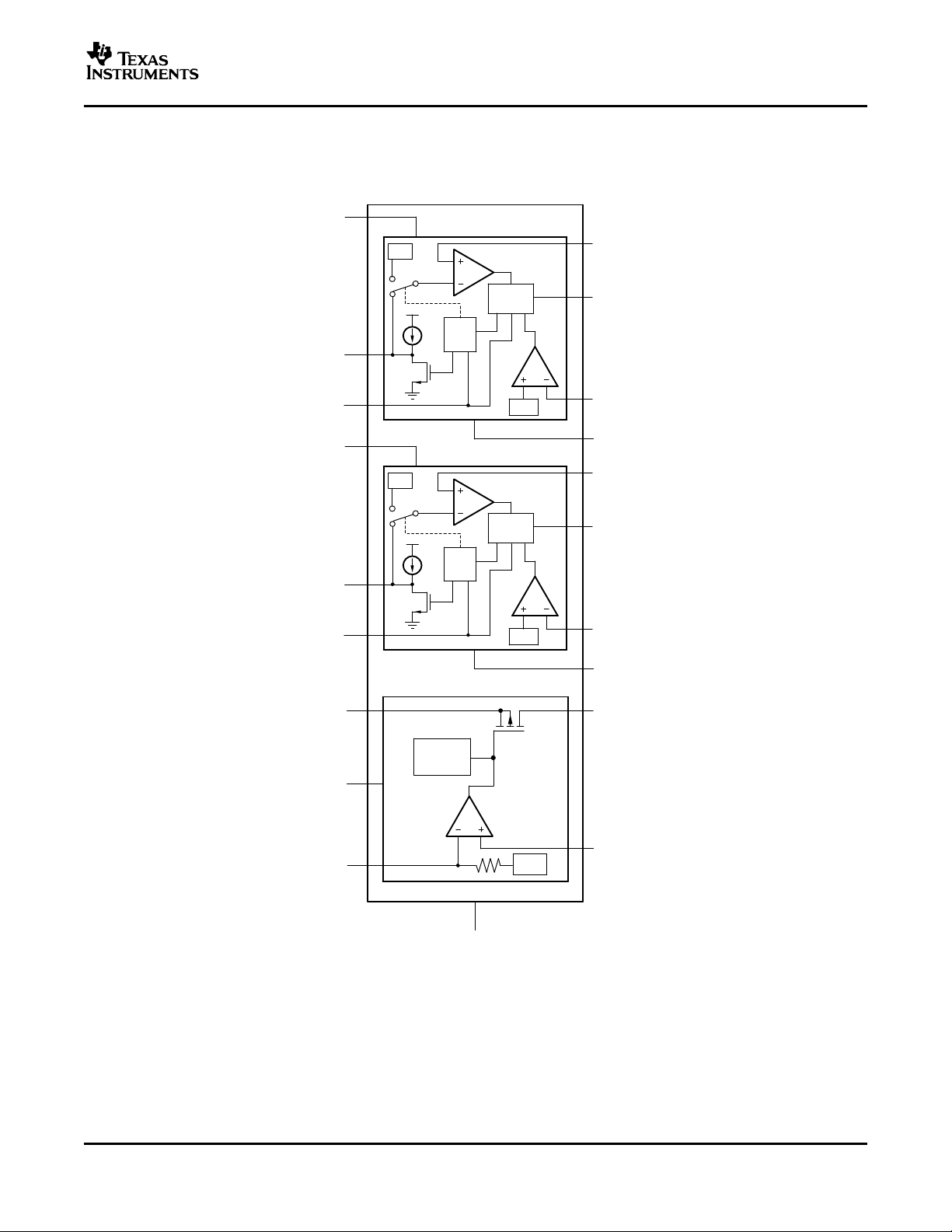
V
RE F1
Soft
Start
Control
Switch
Control
V
IS1
IS1
SW1
FB1
EN1
SS1
IN1
≤
3A Buck Controller
DGND
V
RE F2
Soft
Start
Control
Switch
Control
V
IS2
IS2
SW2
FB2
EN2
SS2
IN2
≤
3A Buck Controller
DGND
FB3
OUT3IN3
EN3
SS3
Thermal/
Current
Limit
300mA LDO
V
REF 3
AGND
TPS75003
TPS75003
SBVS052D – OCTOBER 2004 – REVISED MARCH 2005
DEVICE INFORMATION
Functional Block Diagram
5
Page 6
www.ti.com
IN3
OUT3
FB1
FB2
20
1
11
10
DGND
SS3
AGND
EN1
SS1
DGND
SW1
IN1
IS1
19
18
17
16
15
14
13
12
FB3
EN3
EN2
SS2
DGND
SW2
IN2
IS2
2
3
4
5
6
7
8
9
RHL PACKAGE
4.5mm x 3.5mm QFN
(TOP VIEW)
TPS75003
SBVS052D – OCTOBER 2004 – REVISED MARCH 2005
DEVICE INFORMATION (continued)
TERMINAL
NAME RHL
DGND 6, 15, PAD
AGND 18 Ground connection for LDO.
IN1 13 Input supply to BUCK1.
IN2 8 Input supply to BUCK2.
IN3 20 Input supply to LDO.
EN1 17
EN2 4 Same as EN1 but for BUCK2 controller.
EN3 3 Same as EN1 but for LDO.
SS1 16 slowing the ramp-up of current limit. This high-impedance pin is noise-sensitive; careful layout is
SS2 5 Same as SS1 but for BUCK2 regulator.
SS3 19
IS1 12 to an internal reference to set current limit. For a robust output start-up ramp, careful layout and
IS2 9 Same as IS1 but compared to IN2 and used for BUCK2 controller.
SW1 14 Gate drive pin for external BUCK1 P-channel MOSFET.
SW2 7 Same as SW1 but for BUCK2 controller.
FB1 11 Feedback pin. Used to set the output voltage of BUCK1 regulator.
FB2 10 Same as FB1 but for BUCK2 controller.
FB3 2 Same as FB1 but for LDO.
OUT3 1
TERMINAL FUNCTIONS
DESCRIPTION
Ground connection for BUCK1 and BUCK2 converters. Pins 6 and 15 should be connected to the back
side exposed pad by a short metal trace as shown in the PCB Layout section of this data sheet.
Driving the enable pin (ENx) high turns on BUCK1 regulator. Driving this pin low puts it into shutdown
mode, reducing operating current. The enable pin does not trigger on fast negative going transients.
Connecting a capacitor between this pin and ground increases start-up time of the BUCK1 regulator by
important. See Typical Characteristics, Applications and PCB Layout sections for details.
Connecting a capacitor from this pin to ground slows the start-up time of the LDO reference, therby
slowing output voltage ramp-up. See Applications section for details.
Current sense input for BUCK1 regulator. The voltage difference between this pin and IN1 is compared
bypassing are required. See Applications section for details.
Regulated LDO output. A small ceramic capacitor ( ≥ 2.2µF) is needed from this pin to ground to ensure
stability.
6
Page 7
www.ti.com
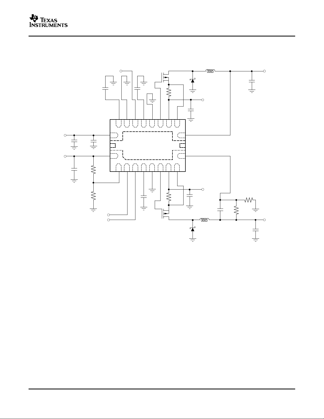
L1
5µH
Sumida
CDRH6D38−5R0
IN3
OUT3
FB1
FB2
20
1
11
10
DGND
SS3
AGND
EN1
SS1
DGND
SW1
IN1
IS1
19
18
17
16
15
14
13
12
FB3
EN3
EN2
SS2
DGND
SW2
IN2
IS2
2
3
4
5
6
7
8
9
R3
61.9k
Ω
R4
15.4k
Ω
EN3
EN2
V
IN
EN1
V
IN
1.5nF
1.5nF
0.01µF
R1
33m
Ω
10pF
100µF
Tantalum
100µF
Tantalum
Siliconix
Si2323DS
Siliconix
Si2323DS
Q2
L2
15µH
Sumida
CDRH8D43−150
V
CCINT
1.2V, 2A
Vishay
SS32
D2
0.1µF
1µF
V
CCAUX
2.5V, 300mA
10µF
0.1µF
R5
61.9k
Ω
ON Semiconductor
MBRM120
R6
36.5k
Ω
V
CCO
3.3V, 2A
R2
33m
Ω
100µF
V
IN
Q1
SBVS052D – OCTOBER 2004 – REVISED MARCH 2005
Typical Application Circuit for Powering the Xilinx Spartan-3 FPGA
TPS75003
Figure 1.
7
Page 8
www.ti.com
0 0.5 1.0 1.5 2.0 2.5 3.0 3.5
I
OUT
(A)
VIN= 3.3V
V
OUT
= 1.2V
TA= +85C
TA=−40C
TA= +25C
5
4
3
2
1
0
−
1
−
2
−
3
−
4
−
5
∆ V
OUT
(%)
0 0.5 1.0 1.5 2.0 2.5 3.0 3.5
I
OUT
(A)
VIN= 5V
V
OUT
= 3.3V
5
4
3
2
1
0
−
1
−
2
−
3
−
4
−
5
∆
V
OUT
(%)
TA= +85C
TA=−40C
TA= +25C
3.0
V
IN
(V)
5
4
3
2
1
0
−
1
−
2
−
3
−
4
−
5
∆
V
OUT
(
%)
V
OUT
= 3.3V
I
OUT
= 2A
3.5 4.0 4.5 5.0 5.5 6.0 6.5 7.0
TA= +85C
TA= +25C
TA=−40C
2.0
V
IN
(V)
5
4
3
2
1
0
−
1
−
2
−
3
−
4
−
5
∆
V
OUT
(
%)
V
OUT
= 1.2V
I
OUT
= 2A
2.5 3.0 3.5 4.0 4.5 5.0 5.5 6.0 6.5 7.0
TA=−40C
TA= +25C
TA= +85C
0 0.5 1.0 1.5 2.0 2.5 3.0
500
400
300
200
100
0
Switching F
requency(kHz)
I
OUT
(A)
V
OUT
= 1.2V
VIN= 3.3V
VIN= 5.0V
−
40C
+25C
+85C
600
500
400
300
200
100
0
Switching Frequency (kHz)
0.01 0.1 1.0 10
I
OUT
(A)
VIN= 5.0V
V
OUT
= 1.2V
VIN= 3.3V
V
OUT
= 1.2V
VIN= 5.0V
V
OUT
= 3.3V
V
OUT
= 1.2V
VIN= 2.2V
TPS75003
SBVS052D – OCTOBER 2004 – REVISED MARCH 2005
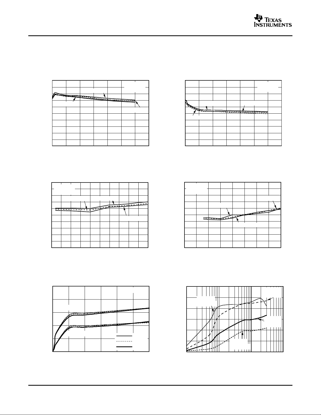
Buck Converter
BUCK LOAD REGULATION BUCK LOAD REGULATION
Figure 2. Figure 3.
TYPICAL CHARACTERISTICS
Measured using circuit in Figure 1
BUCK LINE REGULATION BUCK LINE REGULATION
Figure 4. Figure 5.
BUCK SWITCHING FREQUENCY vs I
, T
OUT
A
BUCK SWITCHING FREQUENCY vs I
OUT
8
Figure 6. Figure 7.
Page 9

www.ti.com
1µs/div
VIN= 5.0V
V
OUT
= 3.3V
I
OUT
= 2A
20mV/div
100
90
80
70
60
50
40
30
20
10
0
Efficiency (%)
0.0001 0.001 0.01 0.1 1 10
I
OUT
(A)
VIN= 5.0V
V
OUT
= 3.3V
VIN= 3.3V
V
OUT
= 1.2V
VIN= 5.0V
V
OUT
= 1.2V
EN
VIN= 5V,C
OUT
= 330µF
VIN= 5V,C
OUT
= 100µF
VIN= 3.3V, C
OUT
= 680µF
VIN= 3.3V,C
OUT
= 100µF
CSS= 0.01µF
V
OUT
= 1.2V
20ms/div
V
OUT
(500mV/div)
EN
VIN= 5V,I
OUT
= 0.5A
VIN= 5V,I
OUT
= 1.0A
VIN= 5V,I
OUT
= 2.0A
VIN= 3.3V, I
OUT
= 1.0A
CSS= 0.01µF
V
OUT
= 1.2V
20ms/div
V
OUT
(500mV/div)
VIN= 3.3V,I
OUT
= 2.0A
EN
VIN= 3.3V,CSS= 0.001µF
VIN= 5V, CSS= 0.001µF
VIN= 5V, CSS= 0.01µF
VIN= 3.3V,CSS= 0.01µF
I
OUT
= 1A
V
OUT
= 1.2V
20ms/div
V
OUT
(500mV/div)
EN
I
OUT
= 2A,
CSS= 560pF
I
OUT
= 0.5A,
CSS= 560pF
I
OUT
= 0.5A, CSS= 1500pF
I
OUT
= 2A, CSS= 1500pF
VIN= 5V
V
OUT
= 3.3V
5ms/div
V
OUT
(2V/div)
TYPICAL CHARACTERISTICS (continued)
Measured using circuit in Figure 1
TPS75003
SBVS052D – OCTOBER 2004 – REVISED MARCH 2005
BUCK OUTPUT VOLTAGE RIPPLE EFFICIENCY vs I
Figure 8. Figure 9.
BUCK START-UP BUCK START-UP
vs vs
VINand I
OUT
VINand C
OUT
OUT
BUCK START-UP BUCK START-UP
Figure 10. Figure 11.
vs vs
VINand C
SS
Figure 12. Figure 13.
I
and C
OUT
SS
9
Page 10

www.ti.com
EN
VIN= 3.3V,
I
OUT
= 1A,
R
S
= 0.020
VIN=5V, I
OUT
= 1A,
RS= 0.033
VIN= 3.3V,
I
OUT
= 1A,
RS= 0.033
V
IN
= 5V,
I
OUT
= 1A,
RS= 0.020
V
OUT
= 1.2V, CSS= 0.01µF
20ms/div
V
OUT
(1V/div)
∆V
OUT
(%)
0 0.05 0.1 0.15 0.2 0.25 0.3 0.35 0.4
5
4
3
2
1
0
−
1
−
2
−
3
−
4
−
5
I
OUT
(A)
VIN= 3.3V
V
OUT
= 2.5V
TA= +25C
TA= +85C
TA=−40C
∆V
OUT
(%)
3.0 3.5 4.0 4.5 5.0 5.5 6.0 6.5 7.0
VIN(V)
V
OUT
= 2.5V
I
OUT
= 1mA
TA= +85C
5
4
3
2
1
0
−
1
−
2
−
3
−
4
−
5
TA= +25C
TA=−40C
450
400
350
300
250
200
150
100
50
0
V
D
O
(mV
)
Ambient Temperature (C)
−40−25−
10 5 20 35 50 65 8580
V
OUT
= 2.5V
I
OUT
= 300mA
500
400
300
200
100
0
V
DO
(mV)
0 50 100 150 200 250 300 350 400 450
I
OUT
(mA)
TA=−40C
TA= +25C
TA= +85C
VIN= 3.3V
V
OUT
= 2.5V
TPS75003
SBVS052D – OCTOBER 2004 – REVISED MARCH 2005
TYPICAL CHARACTERISTICS (continued)
Measured using circuit in Figure 1
LDO Converter
BUCK START-UP
VINand R
vs
SENSE
Figure 14.
LDO LOAD REGULATION LDO LINE REGULATION
LDO DROPOUT vs I
10
Figure 15. Figure 16.
LDO DROPOUT vs T
OUT
Figure 17. Figure 18.
A
Page 11

www.ti.com
2.0 2.5 3.0 3.5 4.0 4.5 5.0 5.5 6.0 6.5 7.0
12
10
8
6
4
2
0
R
DS,ON
( Ω)
VIN(V)
TA=−40C
TA= +25C
TA= +85C
2.0 2.5 3.0 3.5 4.0 4.5 5.0 5.5 6.0 6.5 7.0
12
10
8
6
4
2
0
R
DS, ON
( Ω)
VIN(V)
TA=−40C
TA= +25C
TA= +85C
2.525
2.520
2.515
2.510
2.505
2.500
2.495
2.490
2.485
2.480
2.475
V
OUT
(V)
−
40
−
15 10 35 60 85
Ambient Temperature (C)
VIN= 3.3V
TYPICAL CHARACTERISTICS (continued)
Measured using circuit in Figure 1
R
DS,ON
SBVS052D – OCTOBER 2004 – REVISED MARCH 2005
PMOSvs V
IN
R
NMOSvs V
DS,ON
Figure 19. Figure 20.
TPS75003
IN
LDO V
Figure 21.
vs T
OUT
A
11
Page 12

www.ti.com
TPS75003
SBVS052D – OCTOBER 2004 – REVISED MARCH 2005
APPLICATION INFORMATION
The TPS75003 is an integrated power management IC designed specifically to power DSPs and FPGAs such as
the Xilinx Spartan-3, Spartan-3E and Spartan-3L. Two non-synchronous buck controllers can be configured to
supply up to 3A for both CORE and I/O rails. A low dropout linear regulator powers auxiliary rails up to 300mA.
All channels have independent enable and soft-start, allowing control of inrush current and output voltage ramp
time as required by the application.
Figure 1 shows a typical application circuit for powering the Xilinx Spartan-3 FPGA. Table 1 through Table 4
show component values that have been tested for use with 2A and 3A load currents. Other similar external
components can be substituted as desired; however, in all cases the circuits that are used should be tested for
compliance to application requirements.
Table 1. Inductors Tested with the TPS75003
PART NUMBER MANUFACTURER INDUCTANCE DC RESISTANCE SATURATION CURRENT
SLF7032T–100M1R4 TDK 10µH ± 20% 53m Ω ± 20% 1.4A
SLF6025–150MR88 TDK 15µH ± 20% 85m Ω ± 20% 0.88A
CDRH6D28–5R0 Sumida 5µH 23m Ω 2.4A
CDRH6D38-5R0 Sumida 5µH 18m Ω 2.9A
CDRH103R–100 Sumida 10µH 45m Ω 2.4A
CDRH4D28–100 Sumida 10µH 96m Ω 1.0A
CDRH8D43-150 Sumida 15µH 42m Ω 2.9A
CDRH5D18–6R2 Sumida 6.2µH 71m Ω 1.4A
DO3316P–472 Coilcraft 4.7µH 18m Ω 5.4A
DT3316P–153 Coilcraft 15µH 60m Ω 1.8A
DT3316P–223 Coilcraft 22µH 84m Ω 1.5A
744052006 Würth 6.2µH 80m Ω 1.45A
74451115 Würth 15µH 90m Ω 0.8A
Table 2. PMOS Transistors Tested with the TPS75003
PART NUMBER MANUFACTURER R
Si5447DC Vishay Siliconix 0.11 Ω at VGS = –2.5V –20V –3.5A at +25 ° C 1206
Si5475DC Vishay Siliconix 0.041 Ω at VGS = –2.5V –12V –6.6A at +25 ° C 1206
Si2323DS Vishay Siliconix 0.052 Ω at VGS = –2.5V –20V –4.1A at +25 ° C SOT23
Si2301ADS Vishay Siliconix 0.19 Ω at VGS = –2.5V –20V –1.4A at +25 ° C SOT23
Si2323DS Vishay Siliconix 0.41 Ω at VGS = –2.5V –20V –4.1A at +25 ° C SOT23
FDG326P Fairchild 0.17 Ω at VGS = –2.5V –20V –1.5A SC70
(TYP) V
DS,ON
DS
I
D
PACKAGE
Table 3. Diodes Tested with the TPS75003
PART NUMBER MANUFACTURER V
MBRM120LT3 ON Semiconductor 20V 1.0A DO216AA
MBR0530T1 ON Semiconductor 30V 1.5A SOD123
ZHCS2000TA Zetex 40V 2.0A SOT23–6
B320 Diodes Inc. 20V 3.0A SMA
SS32 Fairchild 20V 3.0A DO214AB
R
I
F
PACKAGE
12
Page 13

www.ti.com
0.1µF
R
D
Q L
f = measured resonant
frequency at switch node
R = 2πfL
TPS75003
SBVS052D – OCTOBER 2004 – REVISED MARCH 2005
Table 4. Capacitors Tested with the TPS75003
PART NUMBER MANUFACTURER CAPACITANCE ESR VOLTAGE RATING
6TPB47M (PosCap) Sanyo 47µF 0.1 Ω 6.3V
T491D476M010AS Kemet 47µF 0.8 Ω 10V
B45197A Epco 47µF 0.175 Ω 16V
B45294–R1107–M40 Epco 100µF 0.045 Ω 6.3V
594D476X0016C2 Vishay 47µF 0.11 Ω 16V
594D127X96R3C2 Vishay 120µF 0.085 Ω 6.3V
TPSC107K006R0150 AVX 100µF 0.15 Ω 6.3V
6TPS100MC Sanyo 100µF 0.45 Ω 6.3V
OPERATION (BUCK CONTROLLERS)
Channels 1 and 2 contain two identical non-synchronous buck controllers that use minimum on-time/minimum
off-time hysteretic control. (Refer to Figure 1 .) For clarity, BUCK1 is used throughout the discussion of device
operation. When V
increasing current through the inductor (L1) until V
reached. Once either of these conditions is met, the PMOS is switched off for at least the minimum off-time of
the device. After the minimum off-time has passed, the output voltage is monitored and the switch is turned on
again when necessary.
When output current is low, the buck controllers operate in discontinuous mode. In this mode, each switching
cycle begins at zero inductor current, rises to a maximum value, then falls back to zero current. When current
reaches zero on the falling edge, ringing occurs at the resonant frequency of the inductor and stray switch node
capacitance. This is normal operation; it does not affect circuit performance, and can be minimized if desired by
using an RC snubber and/or a resistor in series with the gate of the PMOS, as shown in Figure 22 .
is below its target, an external PMOS (Q1) is turned on for at least the minimum on-time,
OUT1
reaches its target value or the current limit (set by R1) is
OUT1
At higher output currents, the TPS75003 operates in continuous mode. In continuous mode, there is no ringing at
the switch node and V
When V
the external PMOS to allow regulation at lower dropout than would otherwise be possible.
Enable (Buck Controllers)
The enable pins (EN1 and EN2) for the buck controllers are active high. When the enable pin is driven low and
input voltage is present at IN1 or IN2, an on-chip FET is turned on to discharge the soft-start pin SS1 or SS2,
respectively. If the soft-start feature is being used, enable should be driven high at least 10 µ s after V
to ensure this discharge cycle occurs.
UVLO (Buck Controllers)
An under-voltage lockout circuit is present to prevent turning on the external PMOS (Q1 or Q2) until a reliable
operating voltage is reached on the appropriate regulator (IN1 or IN2). This prevents the buck controllers from
mis-operation at low input voltages.
Figure 22. RC Snubber and Series Gate Resistor Used to Minimize Ringing
is equal to V
OUT
approaches or falls below V
IN
times the duty cycle of the switching waveform.
IN
, the buck controllers operate in 100% duty cycle mode, fully turning on
OUT
is applied
IN
13
Page 14

www.ti.com
I
LIMIT
V
IS1,2
R
1,2
I
RMS
I
OUT
D I
OUT
V
OUT
V
IN
P
DISS
I
RMS
2
R
TPS75003
SBVS052D – OCTOBER 2004 – REVISED MARCH 2005
Current Limit (Buck Controllers)
An external resistor (R1 or R2) is used to set the current limit for the external PMOS transistor (Q1 or Q2). These
resistors are connected between IN1 and IS1 (or IN2 and IS2) to provide a reference voltage across these pins
that is proportional to the current flowing through the PMOS transistor. This reference voltage is compared to an
internal reference to determine if an over-current condition exists. When current limit is exceeded, the external
PMOS is turned off for the minimum off-time. Current limit detection is disabled for 10ns any time the PMOS is
turned on to avoid triggering on switching noise. In 100% duty cycle mode, current limit is always enabled.
Current limit is calculated using the V
Equation 1 :
The current limit resistor must be appropriately rated for the dissipated power determined by its RMS current
calculated by Equation 2 :
For low-cost applications the I
pin can be connected to the drain of the PMOS, using R
S1,2
R2 to set current limit. Variations in the PMOS R
protect external components such as the inductor, the diode, and the switch itself from damage as a result of
over-current.
or V
IS1
specification in the Electrical Characteristics section, shown in
IS2
instead of R1 or
must be taken into account to ensure that current limit will
DS,ON
DS,ON
(1)
(2)
Short-Circuit Protection (Buck Controllers)
In an overload condition, the current rating of the external components (PMOS, diode, and inductor) can be
exceeded. To help guard against this, the TPS75003 increases its minimum off-time when the voltage at the
feedback pin is lower than the reference voltage. When the output is shorted (V
is zero), minimum off-time is
FB
increased to approximately 4 µ s. The increase in off-time is proportional to the difference between the voltage at
the feedback pin and the internal reference.
Soft-Start (Buck Controllers)
The buck controllers each have independent soft-start capability to limit inrush during start-up and to meet timing
requirements of the Xilinx Spartan-3 FPGA. Limiting inrush current by using soft-start, or by staggering the
turn-on of power rails, also guards against voltage drops at the input source due to its output impedance. Refer
to the soft-start circuitry shown in Figure 23 and the soft-start timing diagram shown in Figure 24 . BUCK 1 will be
discussed in this section; it is identical to BUCK2. Note that pins SS1 and SS2 are very high-impedance and
cannot be probed using a typical oscilloscope setup. When input voltage is applied at IN1 and EN1 is driven low,
any charge on the SS pin is discharged by an on-chip pull-down transistor. When EN1 is driven high, an on-chip
current source starts charging the external soft-start capacitor C
. The voltage on the capacitor is compared to
SS1
the voltage across the current sense resistor R1 to determine if an over-current condition exists. If the voltage
drop across the sense resistor goes above the reference voltage, then the external PMOS is shut off for the
minimum off-time. This implementation provides a cycle-by-cycle current limit and allows the user to program the
soft-start time over a wide range for most applications. For detailed information on choosing C
and C
SS1
SS2
the section, Selecting the Soft-Start Cap.
, see
14
Page 15

www.ti.com
Soft
Start
Control
Switch
Control
V
IS1
EN1
SW1
IS1
IN1
SS1
V
IN
Current
Limit
V
SS1
V
EN1
Time
CIN, MIN
(12)L (I
L
)
2
V
(
RIPPLE
)
V
IN
(12)L 0.3 I
OUT
2
V
(
RIPPLE
)
V
IN
Figure 23. Soft-Start Circuitry
TPS75003
SBVS052D – OCTOBER 2004 – REVISED MARCH 2005
Figure 24. Soft-Start Timing Diagram
Input Capacitor C
, C
IN1
Selection (Buck Controllers)
IN2
It is good analog design practice to place input capacitors near the inputs of the device in order to ensure a low
impedance input supply. 10 µ F to 22 µ F of capacitance for each buck converter is adequate for most applications,
and should be placed within 100mils (0.001in) of the IN1 and IN2 pins to minimize the effects of pulsed current
switching noise on the soft-start circuitry during the first ~1V of output voltage ramp. Low ESR capacitors also
help to minimize noise on the supply line. The minimum value of capacitance can be estimated using Equation 3 :
(3)
15
Page 16

www.ti.com
I
C,IN(RMS)
I
OUT
V
OUT
V
IN,
MIN
VINV
OUTIOUT
r
DS(on)
RL I
OUT
t
(OFF,min)
V
OUTVSCHOTTKY
RL I
OUT
t
ON,
MIN
L
MIN
V
IN
V
OUTIOUT
r
DS(on)
RL I
OUT
t
ON,
MIN
I
L
MIN
V
OUTVSCHOTTKY
RL I
OUT
t
OFF,
MIN
I
I
PMOS(RMS)
I
OUT
D I
OUT
V
OUT
V
IN
P
(cond)
I
OUT
D
2
r
DS(on)
1TC TJ25C
I
OUT
D
r
DS(on)
TPS75003
SBVS052D – OCTOBER 2004 – REVISED MARCH 2005
Note that the capacitors must be able to handle the RMS current in continuous conduction mode, which can be
calculated using Equation 4 :
Inductor Value Selection (Buck Controllers)
The inductor is chosen based on inductance value and maximum current rating. Larger inductors reduce current
ripple (and therefore, output voltage ripple) but are physically larger and more expensive. Inductors with lower
DC resistance typically improve efficiency, but also have higher cost and larger physical size. The buck
converters work well with inductor values between 4.7 µ H and 47 µ H in most applications. When selecting an
inductor, the current rating should exceed the current limit set by R
determine the minimum inductor size, first determine if the device will operate in minimum on-time or minimum
off-time mode. The device will operate in minimum on-time mode if Equation 5 is satisfied:
where R
= the inductor's DC resistance.
L
Minimum inductor size needed when operating in minimum on-time mode is given by Equation 6 :
or R
IS
(see Current Limit section). To
DS,ON
(4)
(5)
Minimum inductor size needed when operating in minimum off-time mode is given by Equation 7 :
External PMOS Transistor Selection (Buck Controllers)
The external PMOS transistor is selected based on threshold voltage (V
capacitance (C
IN1 or IN2 that will be used. A V
) and voltage rating. The PMOS V
G
magnitude that is 0.5V less than the lowest input voltage is normally sufficient.
T
magnitude must be much lower than the lowest voltage at
T
), on-resistance (R
T
), gate
DS,ON
The PMOS gate will see voltages from 0V to the maximum input voltage, so gate-to-source breakdown should be
a few volts higher than the maximum input supply. The drain-to-source of the device will also see this full voltage
swing, and should therefore be a few volts higher than the maximum input supply. The RMS current in the PMOS
can be estimated by using Equation 8 :
The power dissipated in the PMOS is comprised of both conduction and switching losses. Switching losses are
typically insignificant. The conduction losses are a function of the RMS current and the R
DS,ON
of the PMOS, and
are calculated by Equation 9 :
(6)
(7)
(8)
(9)
16
Page 17

www.ti.com
I
(
diode)(RMS)
I
OUT
1D I
OUT
1
V
OUT
V
IN
V
PP
I ESR
1
8 C
OUT
f
1.1I ESR
C
OUT
L I
OUT
2
VINV
OUT
V
R1
1
1
R1
A
1
R1
B
and R1
B
1
1
R1
1
R1
A
R1
A
5
4
R1
TPS75003
SBVS052D – OCTOBER 2004 – REVISED MARCH 2005
Diode Selection (Buck Controllers)
The diode is off when the PMOS is on, and on when the PMOS is off. Since it will be turned on and off at a
relatively high frequency, a Schottky diode is recommended for good performance. The peak current rating of the
diode should exceed the peak current limit set by the sense resistor R
current and low forward voltage at operating current will optimize efficiency. Equation 10 calculates the estimated
average power dissipation:
Output Capacitor Selection (Buck Controllers)
The output capacitor is selected based on output voltage ripple and transient response requirements. As a result
of the nature of the hysteretic control loop, a minimum ESR of a few tens of m Ω should be maintained for good
operation unless a feed-forward resistor is used. Low ESR bulk tantalum or PosCap capacitors work best in most
applications. A 1.0 µ F ceramic capacitor can be used in parallel with this capacitor to filter higher frequency
spikes. The output voltage ripple can be estimated by Equation 11 :
To calculate the capacitance needed to achieve a given voltage ripple as a result of a load transient from zero
output to full current, use Equation 12 :
. A diode with low reverse leakage
IS1,2
(10)
(11)
If only ceramic or other very low ESR output capacitor configurations are desired, additional voltage ripple must
be passed to the feedback pin. This can be accomplished by using the application circuit in Figure 1 . Resistor
R
adds additional control signal to the feedback loop. This circuit works best with R
1B
too low, the output shows worse load regulation. R
Use Equation 14 to calculate R1
Output Voltage Ripple Effect on V
Output voltage ripple causes V
if R1
A
OUT
= (4)(R1
B
(Buck Controllers)
OUT
to be higher or lower than the target value by half of the peak-to-peak voltage
and R
1A
):
A
can be calculated using Equation 13 :
1B
= 2 to 4 x R
1B
. If R
1A
ripple. For minimum on-time, the ripple adds to the voltage; for minimum off-time, it subtracts from the voltage.
Soft-Start Capacitor Selection (Buck Controllers)
BUCK1 is discussed in this section; it is identical to BUCK2. Soft-start is implemented on the buck controllers by
ramping current limit from 0 to its target value (set by R1) over a user-defined time. This time is set by the
external soft-start cap connected to pin SS1. If SS1 is left open, a small on-chip capacitor will provide a current
limit ramp time of approximately 250µs. Figure 25 shows the effects of R1 and SS1 on the current limit start-up
ramp.
(12)
is
1B
(13)
(14)
17
Page 18

www.ti.com
3.0A
Current
Limit
0.7A
Time
R1 = 33mΩ
R1 = 143mΩ
C
SS1
= 0.022µF
C
SS1
= 0.022µF
C
SS1
= 0.01µF
C
SS1
= 0.01µF
V
OUT
V
FB
R
5
R
6
1
TPS75003
SBVS052D – OCTOBER 2004 – REVISED MARCH 2005
Figure 25. Effects of C
and R
SS1
on Current Ramp Limit
1
This soft-start current limit ramo can be used to provide inrush current control or output voltage ramp control.
While the current limit ramp can be easily understood by looking at Figure 25 , the output voltage ramp is a
complex function of many variables. The dominant variables in this process are V
important variables are V
IN1
and L1.
, C
, I
OUT1
SS1
, and R1. Less
OUT1
The best way to set a target start-up time is through bench measurement under target conditions, adjusting C
to get the desired startup profile. To stay above a minimum start-up time, set the nominal start-up time to
approximately five times the minimum. To stay below a maximum time, set the nominal start-up time at one-fifth
of the maximum. Fastest start-up times occur at maximum V
, with minimum V
IN1
, L1, C
OUT1
, C
OUT1
SS1
, and I
Slowest start-up times occur under opposite conditions.
Refer to Figure 10 to Figure 14 for characterization curves showing how the start-up profile is affected by these
critical parameters.
Output Voltage Setting Selection (Buck Controllers)
Output voltage is set using two resistors as shown for Buck2 in Figure 1 . Output voltage is then calculated using
Equation 15 :
where V
= 1.24V.
FB
LDO OPERATION
The TPS75003 LDO uses a PMOS pass element and is offered in an adjustable version for ease of
programming to any output voltage. When used to power V
output voltages to power other circuitry. The LDO has integrated soft-start, independent enable, and short-circuit
and thermal protection. The LDO can be used to power V
signals are used as described in Application Note SLVA159 (available for download from www.ti.com ).
CC,AUX
it is set to 2.5V; it can optionally be set to other
CC,AUX
on the Xilinx Spartan-3 FPGA when 3.3V JTAG
SS1
.
OUT1
(15)
Input Capacitor Selection (LDO)
Although an input capacitor is not required, it is good analog design practice to connect a 0.1 µ F to 10 µ F low ESR
capacitor across the input supply near the regulator. This capacitor counteracts reactive input sources and
improves transient response, stability, and ripple rejection. A higher value capacitor may be needed if large, fast
rise-time load transients are anticipated, or if the device is located far from its power source.
18
Page 19

www.ti.com
V
OUT
V
FB
R
3
R
4
1
TPS75003
SBVS052D – OCTOBER 2004 – REVISED MARCH 2005
Output Capacitor Selection (LDO)
A 2.2 µ F or greater capacitor is required near the output of the device to ensure stability. The LDO is stable with
any capacitor type, including ceramic. If improved transient response or ripple rejection is required, larger and/or
lower ESR output capacitors can be used.
Soft-Start (LDO)
The LDO uses an external soft-start capacitor, C
loop. (See the Functional Block Diagram.) This is a voltage-controlled soft-start, as compared to the
current-controlled soft-start used by the buck controllers.
Setting Output Voltage (LDO)
Output voltage is set using two resistors as shown in Figure 1 . Output voltage is then calculated using
Equation 16 :
where V
= 0.507V.
FB
Internal Current Limit (LDO)
The internal current limit of the LDO helps protect the regulator during fault conditions. When an over-current
condition is detected, the output voltage will be reduced until the current falls to a level that will not damage the
device. For good device reliability, the LDO should not operate at current limit.
, to provide an RC-ramped reference voltage to the control
SS3
(16)
Enable Pin (LDO)
The active high enable pin (EN3) can be used to put the device into shutdown mode. If shutdown and soft-start
capability are not required, EN3 can be tied to IN3.
Dropout Voltage (LDO)
The LDO uses a PMOS transistor to achieve low dropout. When (V
(V
), the pass device is in its linear region of operation, and the input-output resistance is the R
DO
– V
IN
) is less than the dropout voltage
OUT
of the pass
DS,ON
transistor. In this region, the regulator is said to be out of regulation; ripple rejection, line regulation, and load
regulation degrade as (V
– V
IN
) falls much below 0.5V.
OUT
Transient Response (LDO)
The LDO does not have an on-chip pull-down circuit for output is over-voltage conditions. This feature permits
applications that connect higher voltage sources such as an alternate power supply to the output. This design
also results in an output overshoot of several percent if the load current quickly drops to zero. The amplitude of
overshoot can be reduced by increasing C
; the duration of overshoot can be reduced by adding a load
OUT
resistor.
Thermal Protection (LDO)
Thermal protection disables the output when the junction temperature, TJ, reaches unsafe levels. When the
junction cools, the output is again enabled. Depending on power dissipation, thermal resistance, and ambient
temperature, the thermal protection circuit may cycle on and off. This cycling limits the dissipation of the
regulator, protecting it from damage. For good long term reliability, the device should not be continuously
operated at or near thermal shutdown.
19
Page 20

www.ti.com
P
D
V
IN3
V
OUT3
I
OUT3
L1
IN3
OUT3
FB1
FB2
20
1
11
10
DGND
SS3
AGND
EN1
SS1
DGND
SW1
IN1
IS1
19
18
17
16
15
14
13
12
FB3
EN3
EN2
SS2
DGND
SW2
IN2
IS2
2
3
4
5
6
7
8
9
R6
R7
EN3
EN2
V
IN
EN1
V
IN
C5,
C18
C3,
C17
C7
R5
C10
C12, C16
C13, C15
Q1
Q2
L2
V
OUT1
D2
C9
C6
V
OUT3
C14
C8
R9
D1
R8
V
OUT2
R4
C1
V
IN
TPS75003
SBVS052D – OCTOBER 2004 – REVISED MARCH 2005
Power Dissipation (LDO)
The TPS75003 comes in a QFN-style package with an exposed lead frame on the package underside. The
exposed lead frame is the primary path for removing heat and should be soldered to a PC board that is
configured to remove the amount of power dissipated by the LDO, as calculated by Equation 17 :
Power dissipation can be minimized by using the lowest possible input voltage necessary to assure the required
output voltage. The two buck converters do not contribute a significant amount of dissipated power. Using
heavier copper will increase the overall effectiveness of removing heat from the device. The addition of plated
through-holes to heat-dissipating layers will also improve the heatsink effectiveness.
PCB Layout Considerations
As with any switching regulators, careful attention must be paid to board layout. A typical application circuit and
corresponding recommended printed circuit board (PCB) layout with emphasis on the most sensitive areas are
shown in Figure 26 through Figure 28 .
(17)
Note: Most sensitive areas are highlighted by bold lines.
20
Figure 26. Typical Application Circuit
Page 21

www.ti.com
TPS75003
SBVS052D – OCTOBER 2004 – REVISED MARCH 2005
Note: Most sensitive areas are highlighted in green.
Figure 27. Recommended PCB Layout, Component Side, Top View
21
Page 22

www.ti.com
TPS75003
SBVS052D – OCTOBER 2004 – REVISED MARCH 2005
Note: Most sensitive areas are highlighted in green.
Figure 28. Recommended PCB Layout, Bottom Side, Top View
22
Page 23

Page 24

PACKAGE OPTION ADDENDUM
www.ti.com
16-May-2005
PACKAGING INFORMATION
Orderable Device Status
(1)
Package
Type
Package
Drawing
Pins Package
Qty
Eco Plan
TPS75003RHLR ACTIVE QFN RHL 20 3000 Green (RoHS &
no Sb/Br)
TPS75003RHLRG4 ACTIVE QFN RHL 20 3000 Green (RoHS &
no Sb/Br)
TPS75003RHLT ACTIVE QFN RHL 20 250 Green (RoHS &
no Sb/Br)
TPS75003RHLTG4 ACTIVE QFN RHL 20 250 Green (RoHS &
no Sb/Br)
(1)
The marketing status values are defined as follows:
ACTIVE: Product device recommended for new designs.
LIFEBUY: TI has announced that the device will be discontinued, and a lifetime-buy period is in effect.
NRND: Not recommended for new designs. Device is in production to support existing customers, but TI does not recommend using this part in
a new design.
PREVIEW: Device has been announced but is not in production. Samples may or may not be available.
OBSOLETE: TI has discontinued the production of the device.
(2)
Eco Plan - The planned eco-friendly classification: Pb-Free (RoHS) or Green (RoHS & no Sb/Br) - please check
http://www.ti.com/productcontent for the latest availability information and additional product content details.
TBD: The Pb-Free/Green conversion plan has not been defined.
Pb-Free (RoHS): TI's terms "Lead-Free" or "Pb-Free" mean semiconductor products that are compatible with the current RoHS requirements
for all 6 substances, including the requirement that lead not exceed 0.1% by weight in homogeneous materials. Where designed to be soldered
at high temperatures, TI Pb-Free products are suitable for use in specified lead-free processes.
Green (RoHS & no Sb/Br): TI defines "Green" to mean Pb-Free (RoHS compatible), and free of Bromine (Br) and Antimony (Sb) based flame
retardants (Br or Sb do not exceed 0.1% by weight in homogeneous material)
(2)
Lead/Ball Finish MSL Peak Temp
CU NIPDAU Level-1-260C-UNLIM
CU NIPDAU Level-1-260C-UNLIM
CU NIPDAU Level-1-260C-UNLIM
CU NIPDAU Level-1-260C-UNLIM
(3)
(3)
MSL, Peak Temp. -- The Moisture Sensitivity Level rating according to the JEDEC industry standard classifications, and peak solder
temperature.
Important Information and Disclaimer:The information provided on this page represents TI's knowledge and belief as of the date that it is
provided. TI bases its knowledge and belief on information provided by third parties, and makes no representation or warranty as to the
accuracy of such information. Efforts are underway to better integrate information from third parties. TI has taken and continues to take
reasonable steps to provide representative and accurate information but may not have conducted destructive testing or chemical analysis on
incoming materials and chemicals. TI and TI suppliers consider certain information to be proprietary, and thus CAS numbers and other limited
information may not be available for release.
In no event shall TI's liability arising out of such information exceed the total purchase price of the TI part(s) at issue in this document sold by TI
to Customer on an annual basis.
Addendum-Page 1
Page 25

IMPORTANT NOTICE
Texas Instruments Incorporated and its subsidiaries (TI) reserve the right to make corrections, modifications,
enhancements, improvements, and other changes to its products and services at any time and to discontinue
any product or service without notice. Customers should obtain the latest relevant information before placing
orders and should verify that such information is current and complete. All products are sold subject to TI’s terms
and conditions of sale supplied at the time of order acknowledgment.
TI warrants performance of its hardware products to the specifications applicable at the time of sale in
accordance with TI’s standard warranty. Testing and other quality control techniques are used to the extent TI
deems necessary to support this warranty . Except where mandated by government requirements, testing of all
parameters of each product is not necessarily performed.
TI assumes no liability for applications assistance or customer product design. Customers are responsible for
their products and applications using TI components. To minimize the risks associated with customer products
and applications, customers should provide adequate design and operating safeguards.
TI does not warrant or represent that any license, either express or implied, is granted under any TI patent right,
copyright, mask work right, or other TI intellectual property right relating to any combination, machine, or process
in which TI products or services are used. Information published by TI regarding third-party products or services
does not constitute a license from TI to use such products or services or a warranty or endorsement thereof.
Use of such information may require a license from a third party under the patents or other intellectual property
of the third party, or a license from TI under the patents or other intellectual property of TI.
Reproduction of information in TI data books or data sheets is permissible only if reproduction is without
alteration and is accompanied by all associated warranties, conditions, limitations, and notices. Reproduction
of this information with alteration is an unfair and deceptive business practice. TI is not responsible or liable for
such altered documentation.
Resale of TI products or services with statements different from or beyond the parameters stated by TI for that
product or service voids all express and any implied warranties for the associated TI product or service and
is an unfair and deceptive business practice. TI is not responsible or liable for any such statements.
Following are URLs where you can obtain information on other Texas Instruments products and application
solutions:
Products Applications
Amplifiers amplifier.ti.com Audio www.ti.com/audio
Data Converters dataconverter.ti.com Automotive www.ti.com/automotive
DSP dsp.ti.com Broadband www.ti.com/broadband
Interface interface.ti.com Digital Control www.ti.com/digitalcontrol
Logic logic.ti.com Military www.ti.com/military
Power Mgmt power.ti.com Optical Networking www.ti.com/opticalnetwork
Microcontrollers microcontroller.ti.com Security www.ti.com/security
Telephony www.ti.com/telephony
Video & Imaging www.ti.com/video
Wireless www.ti.com/wireless
Mailing Address: Texas Instruments
Post Office Box 655303 Dallas, Texas 75265
Copyright 2005, Texas Instruments Incorporated
 Loading...