

Datasheet TPS73HD325PWPR, TPS73HD325PWP, TPS73HD318PWPR, TPS73HD318PWP, TPS73HD301PWPR Datasheet (Texas Instruments)
...
TPS73HD301, TPS73HD318, TPS73HD325
DUAL-OUTPUT LOW-DROPOUT VOLTAGE REGULATORS
SLVS167C – SEPTEMBER 1998 – REVISED – MAY 1999
D
Dual Output Voltages for Split-Supply
Applications
D
3.3-V/Adjustable Output, 3.3 V/1.8 V, and
3.3 V/2.5
D
Dropout Voltage < 80 mV Max at
I
= 100 mA (3.3-V option)
O
D
Low Quiescent Current, Independent of
Load . . . 340 µA Typ Per Regulator
D
Ultra-Low-Current Sleep State...2 µA Max
D
Dual Active-Low Reset Signals with 200-ms
Pulse Width
D
Output Current Range of 0 mA to 750 mA
Per Regulator
D
28-Pin PowerP AD TSSOP Package
description
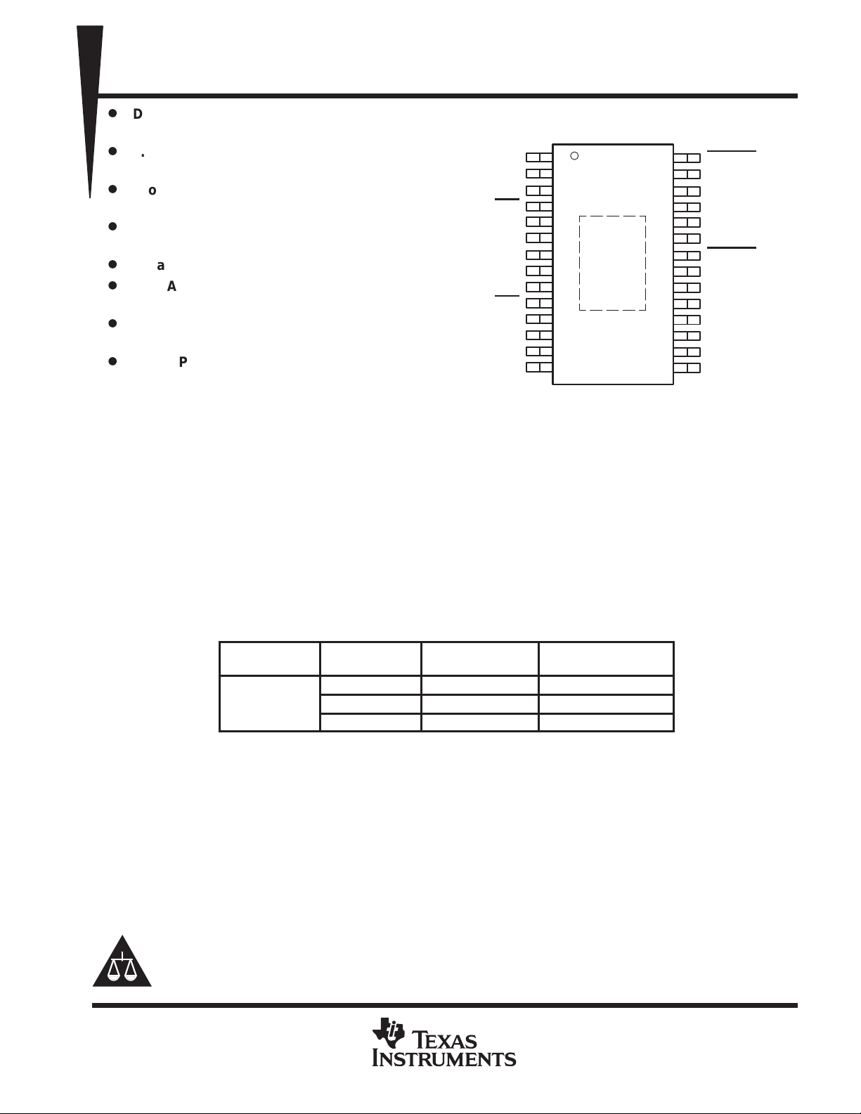
NC
NC
1GND
1EN
1IN
1IN
NC
NC
2GND
2EN
2IN
2IN
NC
NC
NC – No internal connection
PWP PACKAGE
(TOP VIEW)
1
2
3
4
5
6
7
8
9
10
11
12
13
14
28
27
26
25
24
23
22
21
20
19
18
17
16
15
1RESET
NC
NC
1FB/SENSE
1OUT
1OUT
2RESET
NC
NC
2SENSE
2OUT
2OUT
NC
NC
The TPS73HD3xx family of dual voltage regulators offers very low dropout voltages and dual outputs in a
compact package. Designed primarily for DSP applications, these devices can be used in any mixed-output
voltage application with each regulator supporting up to 750 mA. Output current can be allocated as desired
between the two regulators and used to power many of todays DSPs. Low quiescent current and very low
dropout voltage assure maximum power usage in battery-powered applications. T exas Instruments PowerP AD
TSSOP package allows use of these devices with any voltage/current combination within the range of the listed
specifications without thermal problems, provided proper device mounting procedures are followed. Separate
inputs allow the designer to configure the source power as desired. Dual active-low reset signals allow resetting
of core-logic and I/O separately. Remote sense/feedback terminals provide regulation at the load. The
TPS73HD3xx are available in 28-pin PowerPAD TSSOP. They operate over a free-air temperature range of
–40°C to 125°C.
T
A
–40°C to 125°C
Please be aware that an important notice concerning availability, standard warranty, and use in critical applications of
Texas Instruments semiconductor products and disclaimers thereto appears at the end of this data sheet.
PowerPAD is a trademark of Texas Instruments Incorporated.
PRODUCTION DATA information is current as of publication date.
Products conform to specifications per the terms of Texas Instruments
standard warranty. Production processing does not necessarily include
testing of all parameters.
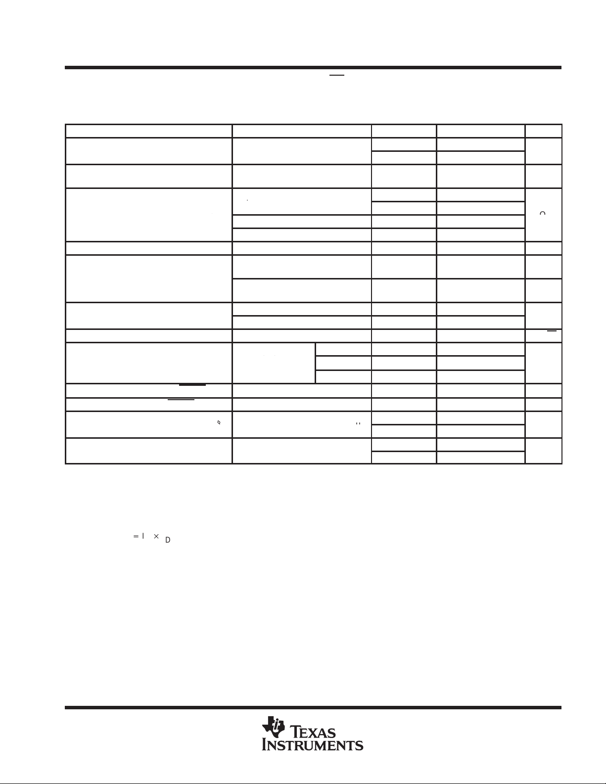
REGULATOR 1
VO (V)
Adj (1.2 – 9.75 V) 3.3 V TPS73HD301PWPR
1.8 V 3.3 V TPS73HD318PWPR
2.5 V 3.3 V TPS73HD325PWPR
AVAILABLE OPTIONS
REGULATOR 2
VO (V)
TSSOP
(PWP)
Copyright 1999, Texas Instruments Incorporated
POST OFFICE BOX 655303 • DALLAS, TEXAS 75265
1
TPS73HD301, TPS73HD318, TPS73HD325
I/O
DESCRIPTION
DUAL-OUTPUT LOW-DROPOUT VOLTAGE REGULATORS
SLVS167C – SEPTEMBER 1998 – REVISED – MAY 1999
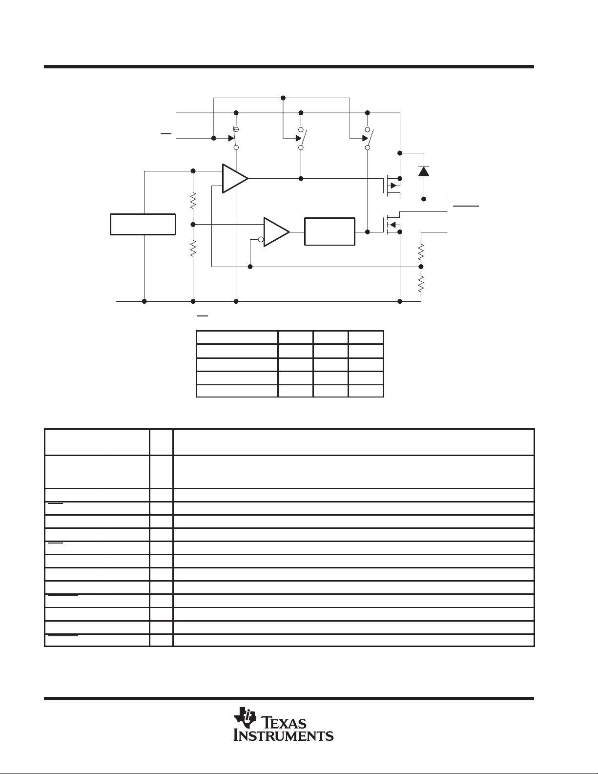
functional block diagram
IN
EN
V
= 1.182 V
ref
GND
†
Switch positions shown with EN
†† †
–
+
low (active).
OUTPUT VOLTAGE
Adjustable 0
1.8 V 122 233 kΩ
2.5 V 260 233 kΩ
3.3 V 420 233 kΩ
R1 R2 UNIT
Delayed
Reset
∞
OUT
RESET
SENSE/FB
R1
R2
Ω
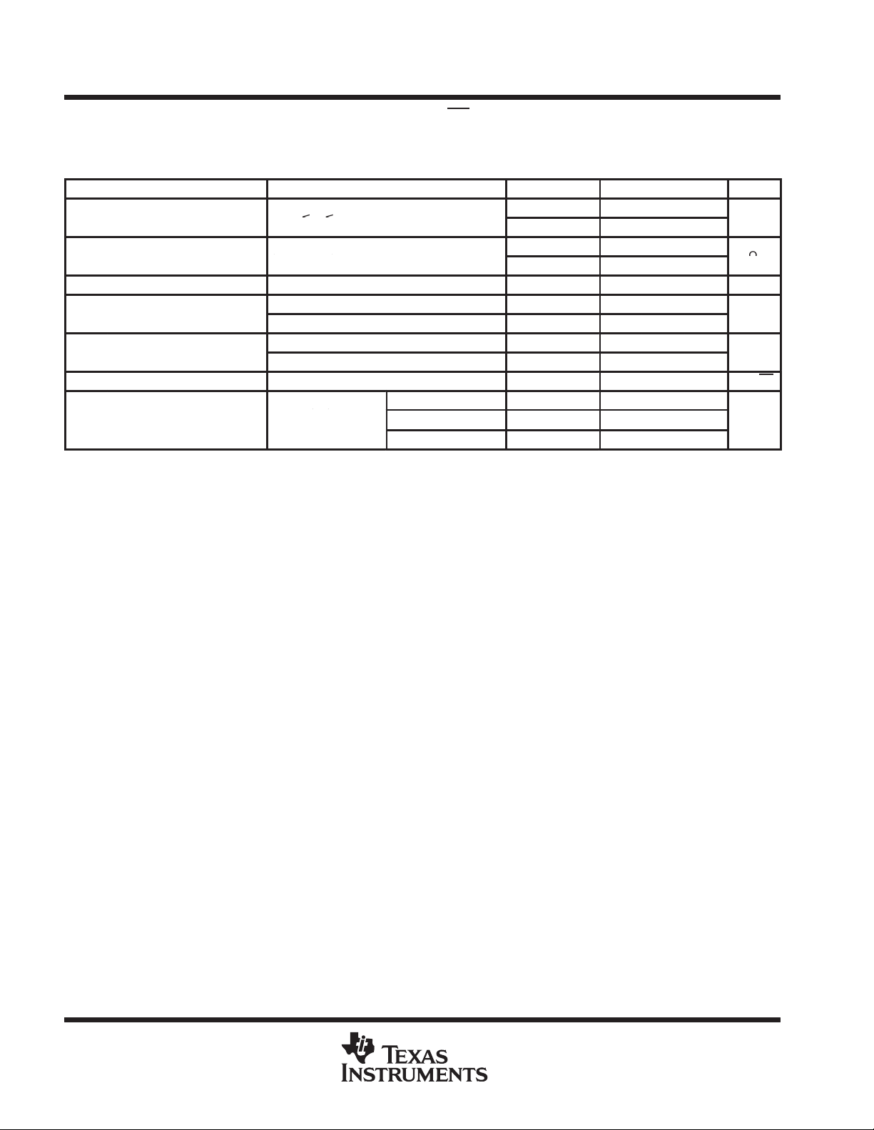
Terminal Functions
TERMINAL
NAME NO.
NC 1, 2, 7, 8,
13–16, 20,
21, 26, 27
1GND 3 Regulator #1 ground
1EN 4 I Regulator #1 enable, low = enable
1IN 5, 6 I Regulator #1 input supply voltage
2GND 9 Regulator #2 ground
2EN 10 I Regulator #2 enable, low = enable
2IN 11, 12 I Regulator #2 input supply voltage
2OUT 17, 18 O Regulator #2 output voltage
2SENSE 19 I Regulator #2 output voltage sense (fixed output)
2RESET 22 O Regulator #2 reset signal, low = reset
1OUT 23, 24 O Regulator #1 output voltage
1FB/SENSE 25 I Regulator #1 output voltage feedback (adjustable output)
1RESET 28 O Regulator #1 reset signal, low = reset
No connection
2
POST OFFICE BOX 655303 • DALLAS, TEXAS 75265
PWP
‡
PWP
§
TPS73HD301, TPS73HD318, TPS73HD325
DUAL-OUTPUT LOW-DROPOUT VOLTAGE REGULATORS
SLVS167C – SEPTEMBER 1998 – REVISED – MAY 1999
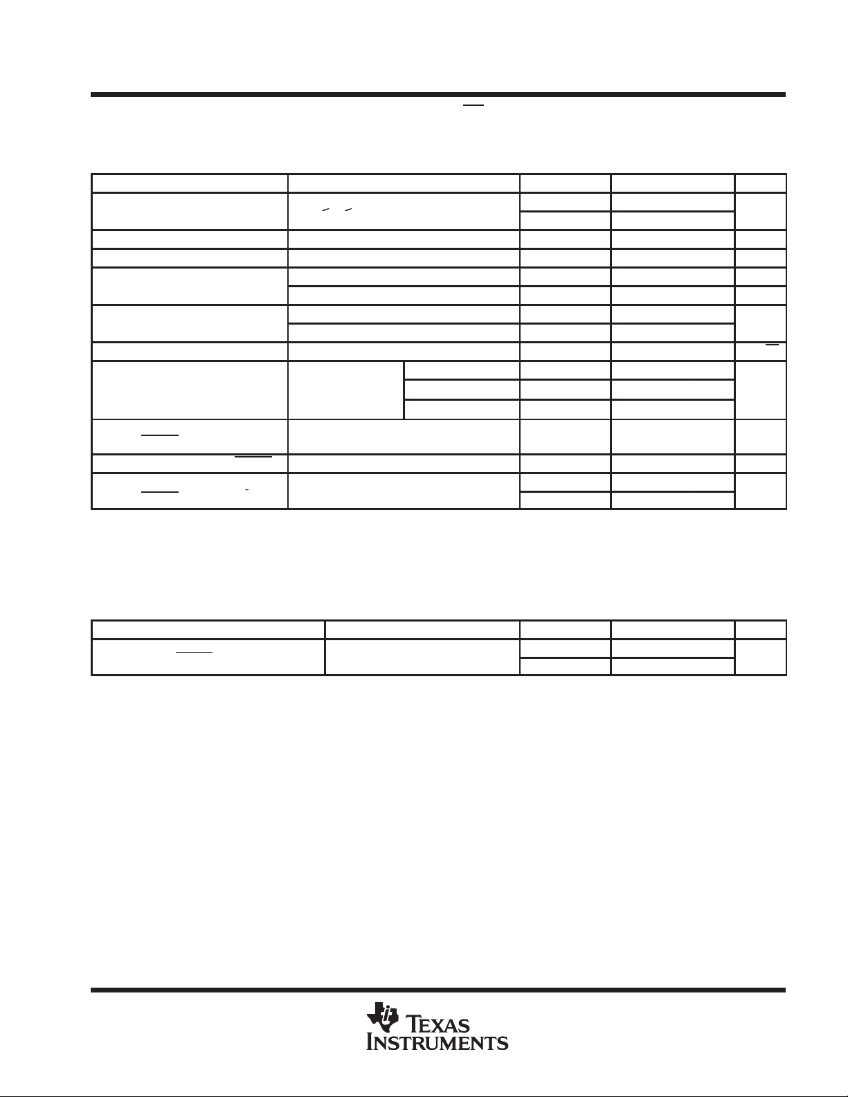
absolute maximum ratings over operating free-air temperature (unless otherwise noted)
Input voltage range, V
Differential input voltage,V
Output current, I
(xIN, xRESET, xSENSE, xEN) –0.3 V to 11 V. . . . . . . . . . . . . . . . . . . . . . . . . . . . . . . . .
I
(1GND to 2GND) 2 V. . . . . . . . . . . . . . . . . . . . . . . . . . . . . . . . . . . . . . . . . . . . . . . . . .
(1OUT, 2OUT) 2 A. . . . . . . . . . . . . . . . . . . . . . . . . . . . . . . . . . . . . . . . . . . . . . . . . . . . . . . . . . . . .
O
ID
†
Continuous total power dissipation See Dissipation Rating Tables. . . . . . . . . . . . . . . . . . . . . . . . . . . . . . . . . . . .
Operating free-air temperature range, T
Storage temperature range, T
–65°C to 150°C. . . . . . . . . . . . . . . . . . . . . . . . . . . . . . . . . . . . . . . . . . . . . . . . . . .
stg
–40°C to 125°C. . . . . . . . . . . . . . . . . . . . . . . . . . . . . . . . . . . . . . . . . . .
A
Lead temperature soldering 1,6 mm (1/16 inch) from case for 10 seconds 260°C. . . . . . . . . . . . . . . . . . . . . . .
†
Stresses beyond those listed under “absolute maximum ratings” may cause permanent damage to the device. These are stress ratings only, and
functional operation of the device at these or any other conditions beyond those indicated under “recommended operating conditions” is not
implied. Exposure to absolute-maximum-rated conditions for extended periods may affect device reliability.
NOTE 1: All voltages are with respect to GND.
DISSIPATION RATING TABLE 1 – FREE-AIR TEMPERATURES
PACKAGE
‡
This parameter is measured with the recommended copper heat sink pattern on a 1-layer PCB, 5-in × 5-in PCB, 1 oz. copper,
2-in × 2-in coverage (4 in2).
§
This parameter is measured with the recommended copper heat sink pattern on a 8-layer PCB, 1.5-in × 2-in PCB, 1 oz. copper
with layers 1, 2, 4, 5, 7, and 8 at 5% coverage (0.9 in2) and layers 3 and 6 at 100% coverage (6 in2).
AIR FLOW
(CFM)
0 2.9 W 23.5 mW/°C 1.9 W 1.5 W
300 4.3 W 34.6 mW/°C 2.8 W 2.2 W
0 3 W 23.8 mW/°C 1.9 W 1.5 W
300 7.2 W 57.9 mW/°C 4.6 W 3.8 W
TA < 25°C
POWER RATING
DERATING FACTOR
ABOVE TA = 25°C
POWER RATING
‡
TA = 70°C
TA = 85°C
POWER RATING
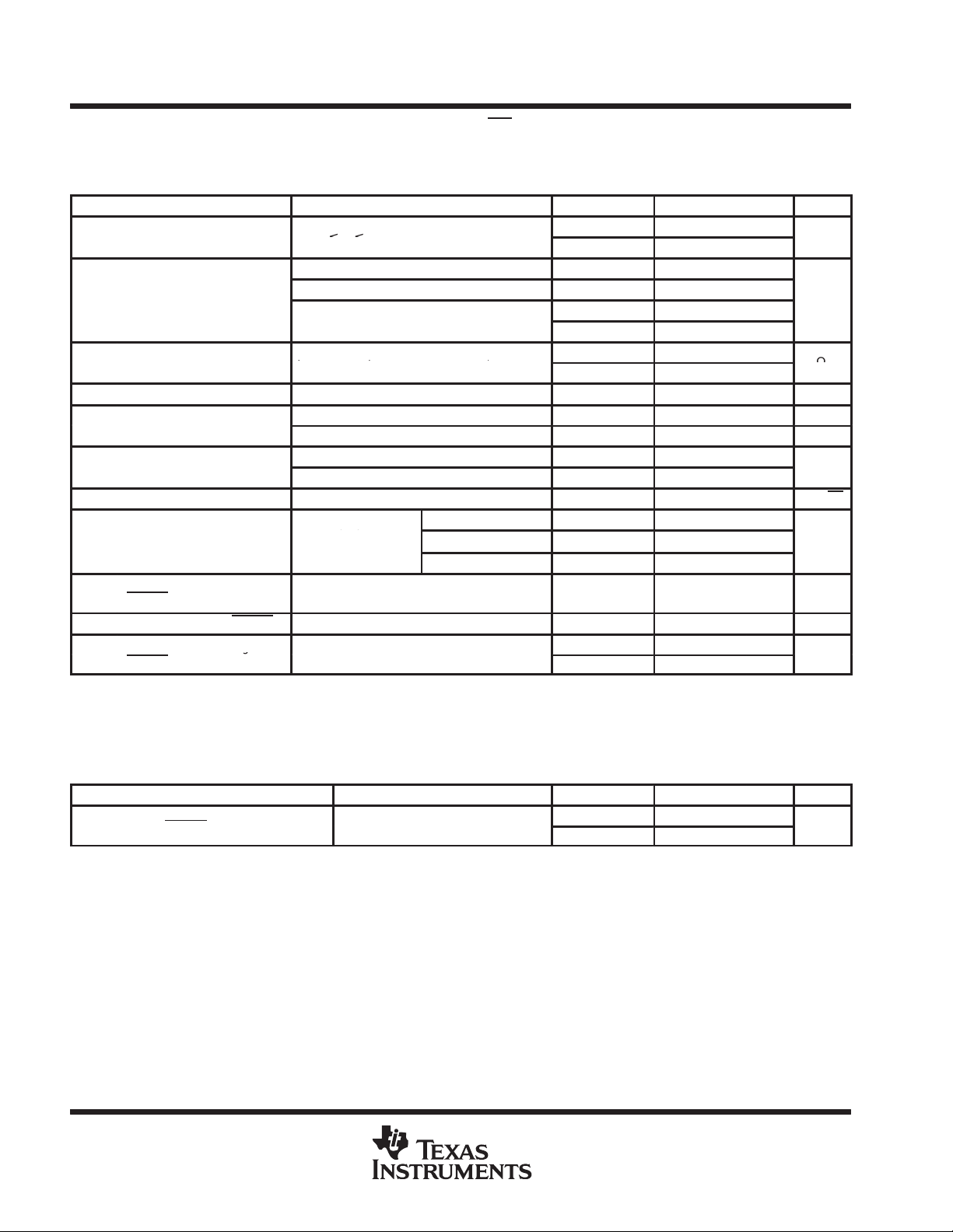
recommended operating conditions
MIN MAX UNIT
V
I(min)
†
I
†
I
+
Input voltage, V
Input voltage, V
High-level input voltage at EN, V
Low-level input voltage at EN, V
Total output current range (per regulator), I
Operating virtual junction temperature range, T
†
Minimum input voltage defined in the recommended operating conditions is the maximum specified output voltage plus dropout voltage, VDO,
at the maximum specified load range (750 mA). Since dropout voltage is a function of output current, the usable range can be extended for lighter
loads. To calculate the minimum input voltage for the maximum load current used in a given application, use the following equation:
Because regulator 1 of the TPS373HD301 is programmable, r
equation for calculating VDO from r
the absolute lower limit for the recommended input voltage range for the TPS73HD301. With 2.97-V input voltage, the LDO may be in dropout
and will not meet the 3% regulaotr output or 750-mA load current specification.
Adjustable output (regulator #1) 2.97 10 V
3.3–V output (regulator #2) 3.97 10 V
IH
IL
O
–40 125 °C
V
O(max)
)
V
DO(max load)
DS(on)
J
should be used to calculate VDO before applying the above equation. The
is given in Note 3 in the TPS73HD301 electrical characteristics table. The minimum value of 3.5 V is
DS(on)
2 V
0.5 V
0 750 mA
POST OFFICE BOX 655303 • DALLAS, TEXAS 75265
3
TPS73HD301, TPS73HD318, TPS73HD325
Quiescent current (active mode), each regulator
0 mA ≤ I
≤ 750 mA
A
ICCSupply current (standby mode), each regulator
I
,
A
IOOutput current limit, each regulator
V
V
V
A
I
Pass-element leakage current (standby mode)
I
,
A
Logic high (EN) (standby mode)
I
,
40°C to 125°C
V
Logic low (EN) (active mode)
See NOTE 2
V
IIInput current (EN)
0 V ≤ V
V
A
Minimum input voltage, for active pass element
V
Minimum input voltage, for valid RESET
I
300 µA
V
DUAL-OUTPUT LOW-DROPOUT VOLTAGE REGULATORS
SLVS167C – SEPTEMBER 1998 – REVISED – MAY 1999
electrical characteristics, V
= 4.3 V, IO = 10 mA, EN = 0 V, CO = 4.7 µF/CSR‡ = 1 Ω,
I(IN)
SENSE/FB shorted to OUT (unless otherwise noted)
= 10
§
,
T
J
25°C 340 415
–40°C to 125°C 550
25°C 0.01 0.5
–40°C to 125°C 2
25°C 0.8 1.2 2
–40°C to 125°C 2
25°C 0.01 0.5
–40°C to 125°C 1
°
–
25°C 0.5
–40°C to 125°C 0.5
25°C –0.5 0.001 0.5
–40°C to 125°C –0.5 0.5
25°C 2.05 2.5
–40°C to 125°C 2.5
25°C 1 1.5
–40°C to 125°C 1.9
MIN TYP MAX UNIT
°
2
2.7
µ
µ
µ
µ
PARAMETER TEST CONDITIONS
EN ≤ 0.5 V,
See NOTE 2
pp
p
lkg
Output voltage temperature coefficient –40°C to 125°C 61 75 ppm/°C
Thermal shutdown junction temperature 165 °C
V
hys
‡
CSR (compensation series resistance) refers to the total series resistance, including the equivalent series resistance (ESR) of the capacitor,
any series resistance added externally, and PWB trace resistance to CO.
§
Pulse-testing techniques are used to maintain virtual junction temperature as close as possible to ambient temperature; thermal effects must
be taken into account separately.
NOTE 2: Minimum input voltage is 3.5V or Vo(typ) + 1V whichever is greater.
The minimum value of 3.5 V is the absolute lower limit for the recommended input voltage range for the TPS73HD301.
Hysteresis voltage (EN) 25°C 50 mV
p
p
p
p
EN = V
NOTE 2
O
EN = V
See NOTE 2
2.5 V ≤ V
6 V ≤ VI ≤ 10 V
O(RESET)
O
,
= 0,
,
≤ 10
I
I
≤ 6 V,
= –
4
POST OFFICE BOX 655303 • DALLAS, TEXAS 75265
Reference voltage (1FB)
O
,
V
µ
O
,
(
Ω
Output regulation
Ripple rejection
dB
CSR = 1 Ω
VOLLow-level output voltage (RESET)
§
V
I
400 µA
V
IIInput current (1FB)
nA
TPS73HD301, TPS73HD318, TPS73HD325
DUAL-OUTPUT LOW-DROPOUT VOLTAGE REGULATORS
SLVS167C – SEPTEMBER 1998 – REVISED – MAY 1999
electrical characteristics, V
= 4.3 V, IO = 10 mA, EN = 0 V, CO = 4.7 µF/CSR† = 1 Ω,
I(IN)
SENSE/FB shorted to OUT (unless otherwise noted) (continued)
adjustable regulator
PARAMETER TEST CONDITIONS
5 mA ≤ I
See NOTE 2
Reference voltage temperature coefficient
50 µA ≤ I
Pass-element series resistance (see
Note 3)
Input regulation VI = 3.5 V, 50 µA ≤ IO ≤ 750 mA 25°C 3 mV
p
pp
Output noise-spectral density f = 120 Hz 25°C 2 mV/√Hz
Output noise voltage
V
Trip-threshold voltage (RESET)
(TO)
V
Hysteresis voltage (RESET)
hys
p
p
†
CSR (compensation series resistance) refers to the total series resistance, including the equivalent series resistance (ESR) of the capacitor,
any series resistance added externally, and PWB trace resistance to CL.
‡
Pulse-testing techniques are used to maintain virtual junction temperature as close as possible to ambient temperature; thermal effects must
be taken into account separately.
§
Output voltage programmed to 2.5 V with closed-loop configuration (see application information)
NOTE 3: To calculate dropout voltage, use equation:
§
See NOTE 2
VI = 3.9 V, 50 µA ≤ IO ≤ 750 mA
VI = 5.9 V, 50 µA ≤ IO ≤ 750 mA 25°C 0.23
IO = 5 mA to 750 mA,
See NOTE 2
IO = 50 µA to 750 mA,
See NOTE 2
f = 120 Hz, IO = 50 µA 25°C 59
f = 120 Hz, IO = 500 mA 25°C 54
10 Hz ≤ f ≤ 100 kHz,
§
V
O(FB)
Measured at V
I
≤ 750 mA,
≤ 750 mA,
=
decreasing –40°C to 125°C 1.101 1.145 V
O(ER)
= 2.13 V,
O(RESET)
‡
CL = 4.7 µF 25°C 95
CL = 10 µF 25°C 89
CL = 100 µF 25°C 74
=
T
J
25°C 1.182
–40°C to 125°C 1.147 1.217
–40°C to 125°C 61 75 ppm/°C
25°C 0.52 1
–40°C to 125°C 1
25°C 0.32
25°C 7 mV
25°C 10 mV
25°C 12 mV
25°C 0.1 0.4
–40°C to 125°C 0.4
25°C –10 0.1 10
–40°C to 125°C –20 20
MIN TYP MAX UNIT
µV/rms
VDO+
r
dropout conditions for programmed output voltages of 4 V and 6 V respectively . For other programmed values, refer to Figure 29.
is a function of both output current and input voltage. This parametric table lists r
DS(ON)
IO
r
DS(ON)
for VI = 3.9 V and 5.9 V , which corresponds to
DS(ON)
POST OFFICE BOX 655303 • DALLAS, TEXAS 75265
5
TPS73HD301, TPS73HD318, TPS73HD325
VOOutput voltage
4.3 V ≤ V
V
V
(
O)O
I
,
Ω
Output regulation
mV
Ripple rejection
dB
CSR = 1 Ω
DUAL-OUTPUT LOW-DROPOUT VOLTAGE REGULATORS
SLVS167C – SEPTEMBER 1998 – REVISED – MAY 1999
electrical characteristics, V
= 4.3 V, IO = 10 mA, EN = 0 V, CO = 4.7 µF/CSR† = 1 Ω, SENSE/FB
I(IN)
shorted to OUT (unless otherwise noted) (continued)
1.8-V regulator (TPS73HD318)
= 3.5 V,
2SENSE
‡
= 0 V
T
J
25°C 1.746 1.8 1.854
–40°C to 125°C 1.728 1.872
§
25°C 0.5 1
–40°C to 125°C 1.2
MIN TYP MAX UNIT
µV/rms
PARAMETER TEST CONDITIONS
p
Pass-element series (3.5 V – V
resistance
Input regulation 50 µA ≤ IO ≤ 750 mA, See NOTE 2 25°C 6 mV
p
pp
Output noise-spectral density f = 120 Hz 25°C 2 mV/√Hz
Output noise voltage
†
CSR (compensation series resistance) refers to the total series resistance, including the equivalent series resistance (ESR) of the capacitor, any
series resistance added externally, and PWB trace resistance to CL.
‡
Pulse-testing techniques are used to maintain virtual junction temperature as close as possible to ambient temperature; thermal effects must
be taken into account separately.
§
Pass-element series resistance measured with sense pin disconnected from output to allow output voltge to rise to full saturation.
IO = 750 mA, V
IO = 5 mA to 750 mA, See NOTE 2 25°C 14
IO = 50 µA to 750 mA, See NOTE 2 25°C 18
f = 120 Hz, IO = 50 µA 25°C 51
f = 120 Hz, IO = 500 mA 25°C 49
10 Hz ≤ f ≤ 100 kHz,
≤ 10
I
)/I
=
V
,
CL = 4.7 µF 25°C 274
CL = 10 µF 25°C 228
CL = 100 µF 25°C 159
6
POST OFFICE BOX 655303 • DALLAS, TEXAS 75265
VOOutput voltage
4.3 V ≤ V
V
V
Output regulation
Ripple rejection
dB
CSR = 1 Ω
V
g
V
I
mA
V
Ti
(RESET)
See Figure 3
ms
TPS73HD301, TPS73HD318, TPS73HD325
DUAL-OUTPUT LOW-DROPOUT VOLTAGE REGULATORS
SLVS167C – SEPTEMBER 1998 – REVISED – MAY 1999
electrical characteristics, V
= 4.3 V, IO = 10 mA, EN = 0 V, CO = 4.7 µF/CSR† = 1 Ω, SENSE/FB
I(IN)
shorted to OUT (unless otherwise noted) (continued)
2.5-V regulator (TPS73HD325)
PARAMETER TEST CONDITIONS
p
Dropout voltage IO = 750 mA, VI = 3.5 V –40°C to 125°C 800 mV
Input regulation 50 µA ≤ IO ≤ 750 mA, See NOTE 2 25°C 6 mV
p
pp
Output noise-spectral density f = 120 Hz 25°C 2 mV/√Hz
Output noise voltage
Trip-threshold voltage
V
(TO)
(RESET
)
V
Hysteresis voltage (RESET) 25°C 18 mV
hys
Low-level output voltage
OL
(RESET)
†
CSR (compensation series resistance) refers to the total series resistance, including the equivalent series resistance (ESR) of the capacitor, any
series resistance added externally, and PWB trace resistance to CL.
‡
Pulse-testing techniques are used to maintain virtual junction temperature as close as possible to ambient temperature; thermal effects must
be taken into account separately.
§
Pass-element series resistance measured with sense pin disconnected from output to allow output voltge to rise to full saturation.
IO = 5 mA to 750 mA, See NOTE 2 25°C 20 mV
IO = 50 µA to 750 mA, See NOTE 2 25°C 25 mV
f = 120 Hz, IO = 50 µA 25°C 51
f = 120 Hz, IO = 500 mA 25°C 49
10 Hz ≤ f ≤ 100 kHz,
VO decreasing –40°C to 125°C 2.172 V
I
=
= 2.8 V,
≤ 10
I
CL = 4.7 µF 25°C 274
CL = 10 µF 25°C 228
CL = 100 µF 25°C 159
‡
O(RESET)
= –1
T
J
25°C 2.45 2.5 2.55
–40°C to 125°C 2.425 2.575
25°C 0.17 0.4
–40°C to 125°C 0.4
MIN TYP MAX UNIT
µV/rms
switching characteristics
PARAMETER TEST CONDITIONS T
me-out delay
J
25°C 140 200 260
–40°C to 125°C 100 300
MIN TYP MAX UNIT
POST OFFICE BOX 655303 • DALLAS, TEXAS 75265
7
TPS73HD301, TPS73HD318, TPS73HD325
VOOutput voltage
4.3 V ≤ V
V
V
Dropout voltage
mV
I
750 mA
V
3.23 V
(
O)O
I
,
Ω
Output regulation
Ripple rejection
dB
CSR = 1 Ω
V
g
V
I
mA
V
Ti
(RESET)
See Figure 3
ms
DUAL-OUTPUT LOW-DROPOUT VOLTAGE REGULATORS
SLVS167C – SEPTEMBER 1998 – REVISED – MAY 1999
electrical characteristics, V
= 4.3 V, IO = 10 mA, EN = 0 V, CO = 4.7 µF/CSR† = 1 Ω, SENSE/FB
I(IN)
shorted to OUT (unless otherwise noted) (continued)
3.3-V regulator (TPS73HD301)
PARAMETER TEST CONDITIONS
p
IO = 10 mA, VI = 3.23 V 25°C 4.5 10
p
Pass-element series (3.23 V – V
resistance
Input regulation 50 µA ≤ IO ≤ 750 mA, See NOTE 2 25°C 6 mV
p
pp
Output noise-spectral density f = 120 Hz 25°C 2 mV/√Hz
Output noise voltage
Trip-threshold voltage
V
(TO)
(RESET
)
V
Hysteresis voltage (RESET) 25°C 18 mV
hys
Low-level output voltage
OL
(RESET)
†
CSR (compensation series resistance) refers to the total series resistance, including the equivalent series resistance (ESR) of the capacitor, any
series resistance added externally, and PWB trace resistance to CL.
‡
Pulse-testing techniques are used to maintain virtual junction temperature as close as possible to ambient temperature; thermal effects must
be taken into account separately.
IO = 100 mA, VI = 3.23 V 25°C 44 100
O
IO = 750 mA
IO = 5 mA to 750 mA, See NOTE 2 25°C 30 mV
IO = 50 µA to 750 mA, See NOTE 2 25°C 37 mV
f = 120 Hz, IO = 50 µA 25°C 51
f = 120 Hz, IO = 500 mA 25°C 49
10 Hz ≤ f ≤ 100 kHz,
VO decreasing –40°C to 125°C 2.868 V
=
=
= 2.8 V,
I
≤ 10
I
,
)/I
V
,
CL = 4.7 µF 25°C 274
CL = 10 µF 25°C 228
CL = 100 µF 25°C 159
‡
=
I
= 3.23 V,
O(RESET)
= –1
T
J
25°C 3.3
–40°C to 125°C 3.23 3.37
25°C 353 750
–40°C to 125°C 800
25°C 0.44 1
–40°C to 125°C 1.07
25°C 0.17 0.4
–40°C to 125°C 0.4
MIN TYP MAX UNIT
µV/rms
switching characteristics
me-out delay
8
PARAMETER TEST CONDITIONS T
POST OFFICE BOX 655303 • DALLAS, TEXAS 75265
J
25°C 140 200 260
–40°C to 125°C 100 300
MIN TYP MAX UNIT
TPS73HD301, TPS73HD318, TPS73HD325
DUAL-OUTPUT LOW-DROPOUT VOLTAGE REGULATORS
SLVS167C – SEPTEMBER 1998 – REVISED – MAY 1999
PARAMETER MEASUREMENT INFORMATION
V
O
V
RESET
V
I
IN
RESET
250 kΩ
IT+
t
0.1 µf
EN
SENSE
GND
TEST CIRCUIT
OUT
+
CSR
V
O
10 µF
RESET
Figure 1. Test Circuit and Voltage Waveforms
V
I
†
IN
EN
GND
Ceramic capacitor
OUT
SENSE
+
CSR
C
O
RESET
Timeout Delay
VOLTAGE WAVEFORMS
†
C
CER
RL
t
Figure 2. Test Circuit for Typical Regions of Stability (Refer to Figures 29 through 32)
POST OFFICE BOX 655303 • DALLAS, TEXAS 75265
9

TPS73HD301, TPS73HD318, TPS73HD325
IQQuiescent current
VDODropout voltage
Load transient response
Line transient response
C
(CSR)
DUAL-OUTPUT LOW-DROPOUT VOLTAGE REGULATORS
SLVS167C – SEPTEMBER 1998 – REVISED – MAY 1999
TYPICAL CHARACTERISTICS
Table of Graphs
Adjustable regulator vs Load current 7
3.3-V regulator vs Load current 8
Adjustable regulator 17
3.3-V regulator 18
Adjustable regulator 19
3.3-V regulator 20
Adjustable regulator
3.3-V regulator vs Output current 26
Adjustable regulator vs Added ceramic capacitance 27
3.3-V regulator vs Added ceramic capacitance 28
∆V
DO
V
DO
∆V
O
V
O
V
O
r
DS(on)
V
I
V
IT–
I
OL(RESET)
t
d
t
d
p
Change in dropout voltage vs Free-air temperature 9
Dropout voltage vs Output current 10
Change in output voltage vs Free-air temperature 11
Output voltage vs Input voltage 12
Line regulation 13
Output voltage vs Output current 14, 15
Output voltage response from enable (EN) 16
p
p
Ripple rejection vs Frequency 21
Output spectral noise density vs Frequency 22
ompensation series resistance
Pass-element resistance vs Input voltage 29
Minimum input voltage for valid RESET vs Free-air temperature 30
Negative-going reset threshold vs Free-air temperature 31
RESET output current 3.3-V regulato vs Input voltage 32
Reset time delay vs Free-air temperature 33
Distribution for reset delay 34
vs Load current 5
vs Input voltage 6
vs Output current 23
vs Added ceramic capacitance 24
vs Output current 25
10
POST OFFICE BOX 655303 • DALLAS, TEXAS 75265

TPS73HD301, TPS73HD318, TPS73HD325
DUAL-OUTPUT LOW-DROPOUT VOLTAGE REGULATORS
SLVS167C – SEPTEMBER 1998 – REVISED – MAY 1999
TYPICAL CHARACTERISTICS
QUEISCENT CURRENT
vs
LOAD CURRENT
500
450
400
350
300
250
200
150
Q
I – Queiscent Current – uA
100
50
0
0 200 400 600 800
Adjustable With V
Programmed to 2.5 V
IO – Load Current – mA
O
3.3-V Regulator
Figure 3
VI = 4.3 V
QUIESCENT CURRENT
INPUT VOLTAGE
500
TA = 25°C
IO = 500 mA
450
400
Aµ
350
300
250
200
– Quiescent Current –
150
Q
I
100
50
3.3-V Regulator
0
0123456
VI – Input Voltage – V
Figure 4
vs
Adjustable With V
Programmed to 2.5 V
O
78910
ADJUSTABLE REGULATOR DROPOUT VOLTAGE
vs
LOAD CURRENT
0.6
0.5
0.4
TA = 25°C
TA = –40°C
500 600 700
0.3
0.2
Dropout Voltage – V
0.1
0
TA = 125°C
0 100 200 300 400
Load Current – mA
Figure 5
0.6
0.5
0.4
0.3
0.2
Dropout Voltage – V
0.1
0
3.3–V REGULATOR DROPOUT VOLTAGE
vs
LOAD CURRENT
TA = 125°C
TA = 25°C
TA = –40°C
0 100 200 300 400
Load Current – mA
500 600 700
Figure 6
POST OFFICE BOX 655303 • DALLAS, TEXAS 75265
11

TPS73HD301, TPS73HD318, TPS73HD325
DUAL-OUTPUT LOW-DROPOUT VOLTAGE REGULATORS
SLVS167C – SEPTEMBER 1998 – REVISED – MAY 1999
TYPICAL CHARACTERISTICS
CHANGE IN DROPOUT VOLTAGE
vs
FREE-AIR TEMPERATURE
10
IO = 100 mA
8
6
4
2
0
–2
–4
– Change In Dropout Voltage – mV
–6
DO
V
∆
–8
–10
–50 – 25 0 25 50 75 100 125
TA – Free-Air Temperature – ° C
Figure 7
CHANGE IN OUTPUT VOLTAGE
vs
FREE-AIR TEMPERATURE
20
VI = V
IO = 100 mA
15
10
5
O(nom)
+ 1 V
DROPOUT VOLTAGE
vs
OUTPUT CURRENT
1.6
TA = 25°C
1.4
1.2
1
0.8
0.6
– Dropout Voltage – VV
0.4
DO
0.2
0
0 50 100 150 200 250
VI = 3.9 V
VI = 5.9 V
VI = 9.65 V
IO – Output Current – mA
Figure 8
OUTPUT VOLTAGE
vs
INPUT VOLTAGE
6
TA = 25°C
IO = 500 mA
5
4
3.3-V Regulator
–10
– Change in Output Voltage – mV
O
V
–15
∆
–20
12
0
–5
–50 –25 0 25 50 75 100 125
TA – Free-Air Temperature – ° C
Figure 9
POST OFFICE BOX 655303 • DALLAS, TEXAS 75265
3
2
– Output Voltage – V
O
V
1
0
2.5 V Regulator and
Adjustable With V
Programmed to 2.5 V
0123456
VI – Input Voltage – V
Figure 10
O
78910

TPS73HD301, TPS73HD318, TPS73HD325
DUAL-OUTPUT LOW-DROPOUT VOLTAGE REGULATORS
SLVS167C – SEPTEMBER 1998 – REVISED – MAY 1999
TYPICAL CHARACTERISTICS
OUTPUT VOLTAGE
vs
OUTPUT CURRENT
VI = 10 V
20
TA = 25°C
IO = 250 mA
15
3.3-V Regulator
10
5
0
LINE REGULATION
2.55
Adjustable Regulator
2.54
2.53
2.52
2.51
VI = 3.5 V
2.5
–5
–10
– Change In Output Voltage – mV
O
∆V
–15
–20
4567
VI – Input Voltage – V
Figure 11
8910
3.38
3.36
3.34
3.32
3.30
3.28
O
V – Output voltage – V
3.26
3.3-V Regulator
VI = 10 V
2.49
O
2.48
V – Output voltage – V
2.47
2.46
2.45
0 200 400 600 800
OUTPUT VOLTAGE
vs
OUTPUT CURRENT
VI = 4.3 V
IO – Output Current – mA
Figure 12
3.24
3.22
0 200 400 600 800
IO – Output Current – mA
Figure 13
POST OFFICE BOX 655303 • DALLAS, TEXAS 75265
13

TPS73HD301, TPS73HD318, TPS73HD325
DUAL-OUTPUT LOW-DROPOUT VOLTAGE REGULATORS
SLVS167C – SEPTEMBER 1998 – REVISED – MAY 1999
TYPICAL CHARACTERISTICS
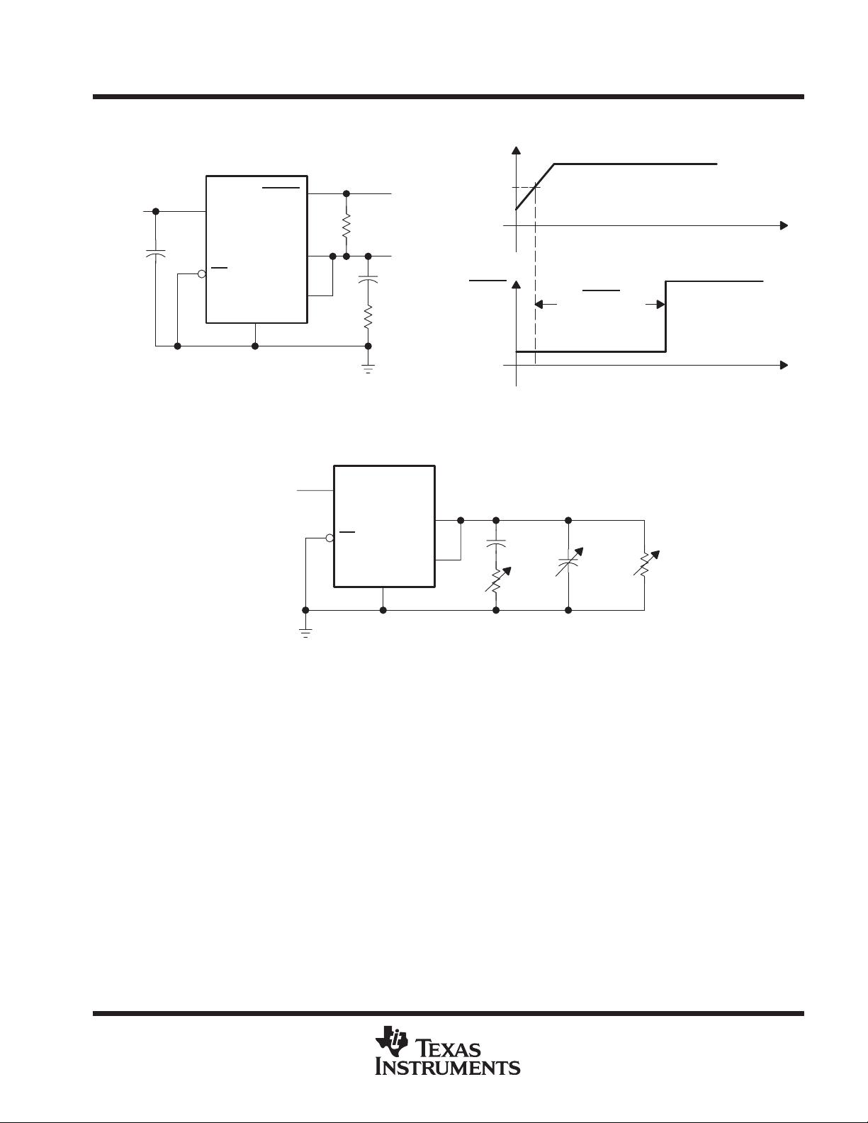
OUTPUT VOLTAGE RESPONSE FROM
ENABLE (EN)
6
4
2
– Output Voltage – V
0
O
V
V
O(nom)
TA = 25°C
RL = 500 Ω
Co = 4.7 µF (CSR = 1Ω)
No Input Capacitance
6
4
2
0
EN Voltage – V
o
∆V – Change in Output V oltage – mV
1500
1000
500
–500
–1000
–1500
–2000
–2500
0 20 40 60 80 100 120 140
Time – µs
–2
Figure 14
ADJUSTABLE REGULATOR
LOAD TRANSIENT RESPONSE
2000
1500
1000
o
∆V – Change in Output V oltage – mV
500
0
–500
–1000
–1500
–2000
0
TA = 25°C
VI = 6 V
∆IO = 750 mA
Co = 10 µF
CSR = 1 Ohm
tR = 50 ns
200100
0
t – time – us
300 400 500 600
Figure 15
3.3–V REGULATOR
LOAD TRANSIENT RESPONSE
TA = 25°C
VI = 6 V
∆IO = 750 mA
Co = 10 µF
CSR = 1 Ohm
tR = 50 ns
200100
0
t – time – us
300 400 500 600
Figure 16
14
POST OFFICE BOX 655303 • DALLAS, TEXAS 75265

TPS73HD301, TPS73HD318, TPS73HD325
DUAL-OUTPUT LOW-DROPOUT VOLTAGE REGULATORS
SLVS167C – SEPTEMBER 1998 – REVISED – MAY 1999
TYPICAL CHARACTERISTICS
ADJUSTABLE REGULATOR
LINE TRANSIENT RESPONSE
100
50
0
– Change in Output Voltage – mV∆ V
– Change in Output Voltage – mV∆V
O
O
–50
–100
200
100
–50
–100
TA = 25°C
CI = 0
Co = 4.7 µF (CSR = 1 Ω)
VO Programmable to 2.5 V
0 100 200 300 400
3.3-V REGULATOR
LINE TRANSIENT RESPONSE
0
t – Time – µs
Figure 17
TA = 25°C
CI = 0
Co = 4.7 µF (CSR = 1 Ω)
6.5
6.25
6
5.75
6.5
– Input Voltage – V
I
V
0 100 200 300 400 500
t – Time – µs
Figure 18
POST OFFICE BOX 655303 • DALLAS, TEXAS 75265
6.25
6
5.75
– Input Voltage – V
I
V
15

TPS73HD301, TPS73HD318, TPS73HD325
DUAL-OUTPUT LOW-DROPOUT VOLTAGE REGULATORS
SLVS167C – SEPTEMBER 1998 – REVISED – MAY 1999
TYPICAL CHARACTERISTICS
RIPPLE REJECTION
vs
FREQUENCY
60
3.3-V Regulator
50
40
30
20
Ripple Rejection – dB
10
0
10 100 1 K 10 K 100 K 1 M 10 M
f – Frequency – Hz
TA = 25°C
No Input
Capacitance Added
VI = VO + 1 V
IO = 100 mA
Co = 4.7 µF (CSR = 1)
Adjustable With
VO Programmed
to 2.5 V
Figure 19
TYPICAL REGIONS OF STABILITY
COMPENSATION SERIES RESISTANCE (CSR)
vs
OUTPUT CURRENT
100
Region of Instability
10
OUTPUT SPECTRAL-NOISE DENSITY
vs
FREQUENCY
10
Hzµ
V/
1
0.1
Output Spectral-Noise Density –
Co = 100 µF (CSR = 1 Ω)
0.01
10 100 1 k 10 k 100 k
TA = 25°C
No Input Capacitance Added
VI = VO + 1 V
Co = 4.7 µF (CSR = 1 Ω)
Co = 10 µF (CSR = 1 Ω)
f – Frequency – Hz
Figure 20
†
COMPENSATION SERIES RESISTANCE (CSR)
100
10
TYPICAL REGIONS OF STABILITY
vs
ADDED CERAMIC CAPACITANCE
Region of
Instability
TA = 25°C
VI = VO + 1 V
IO = 500 mA
Co = 4.7 µF
No Input Capacitor Added
†
16
1
TA = 25°C
0.1
CSR – Compensation Series Resistance – Ω
0.01
Region of Instability
0 50 100 150 200 250
VI = VO + 1 V
Co = 4.7 µF
No Added Ceramic Capacitance
No Input Capacitance Added
IO – Output Current – mA
Figure 21
POST OFFICE BOX 655303 • DALLAS, TEXAS 75265
1
0.1
CSR – Compensation Series Resistance – Ω
0.01
0 0.1 0.2 0.3 0.4 0.5
Added Ceramic Capacitance – µF
Region of Instability
0.6 0.7 0.8 0.9 1
Figure 22

Y
TPS73HD301, TPS73HD318, TPS73HD325
DUAL-OUTPUT LOW-DROPOUT VOLTAGE REGULATORS
SLVS167C – SEPTEMBER 1998 – REVISED – MAY 1999
TYPICAL CHARACTERISTICS
ADJUSTABLE REGULATOR TYPICAL REGIONS OF STABILITY
COMPENSATION SERIES RESISTANCE
vs
OUTPUT CURRENT
100
Region of Instability
10
1
0.1
CSR – Compensation Series Resistance – Ω
0.01
0 200 400 600
100 300 500 700
Region of Instability
IO – Output Current – mA
TA = 25°C
VI = VO + 1 V
Co = 10 µF
No added ceramic
capacitance.
No input capacitor.
Figure 23
3.3–V REGULATOR TYPICAL REGIONS OF STABILITY
COMPENSATION SERIES RESISTANCE
vs
OUTPUT CURRENT
100
Region of Instability
10
TA = 25°C
VI = VO + 1 V
1
0.1
CSR – Compensation Series Resistance – Ω
0.01
0 200 400 600
100 300 500 700
Region of Instability
IO – Output Current – mA
Co = 10 µF
No added ceramic
capacitance.
No input capacitor.
Figure 24
ADJUSTABLE REGULATOR TYPICAL REGIONS OF STABILIT
COMPENSATION SERIES RESISTANCE
vs
ADDED CERAMIC CAPACITANCE
100
Region of Instability
10
TA = 25°C
VI = VO + 1 V
1
IO = 750 mA
Co = 10 µF
No input capacitance.
0.1
CSR – Compensation Series Resistance – Ω
0.01
0 0.4 0.8
Region of Instability
0.2 0.6 1
Added Ceramic Capacitance – µF
Figure 25
3.3-V REGULATOR TYPICAL REGIONS OF STABILITY
COMPENSATION SERIES RESISTANCE
vs
ADDED CERAMIC CAPACITANCE
100
10
TA = 25°C
VI = VO + 1 V
1
IO = 750 mA
Co = 10 µF
No input capacitance.
0.1
CSR – Compensation Series Resistance – Ω
0.01
0 0.4 0.8
0.2 0.6 1
Added Ceramic Capacitance – µF
Region of Instability
Region of Instability
Figure 26
POST OFFICE BOX 655303 • DALLAS, TEXAS 75265
17

TPS73HD301, TPS73HD318, TPS73HD325
DUAL-OUTPUT LOW-DROPOUT VOLTAGE REGULATORS
SLVS167C – SEPTEMBER 1998 – REVISED – MAY 1999
TYPICAL CHARACTERISTICS
PASS-ELEMENT RESISTANCE
vs
INPUT VOLTAGE
1.1
1
Ω
0.9
0.8
0.7
0.6
0.5
0.4
– Pass-Element Resistance –
0.3
DS(on)
r
0.2
0.1
2457
368
IO = 500 mA
IO = 100 mA
VI – Input Voltage – V
Figure 27
NEGATIVE-GOING RESET THRESHOLD
vs
FREE-AIR TEMPERATURE
15
10
T
= 25°C
A
V
= 1.12 V
I(FB)
910
MINIMUM INPUT VOLTAGE FOR VALID RESET
vs
FREE-AIR TEMPERATURE
1.1
1.09
1.08
1.07
1.06
– Minimum Input Voltage For Valid RESET – V
I
V
1.05
–50 –25 0 25 50 75 100 125
TA – Free-Air Temperature – ° C
Figure 28
RESET OUTPUT CURRENT
vs
INPUT VOLTAGE
4
IL = 10 mA
VOL ≤ 0.4 V
3.5
TA = 25°C
3.3-V Regulator
3
5
0
–5
– Negative-Going Reset Threshold – mV
–10
IT–
V
–15
–50 –25 0 25 50 75 100 125
TA – Free-Air Temperature – ° C
Figure 29
18
2.5
2
1.5
– RESET Output Current – mA
1
OL
I
0.5
0
0123456
POST OFFICE BOX 655303 • DALLAS, TEXAS 75265
78910
VI – Input Voltage – V
Figure 30

TPS73HD301, TPS73HD318, TPS73HD325
DUAL-OUTPUT LOW-DROPOUT VOLTAGE REGULATORS
SLVS167C – SEPTEMBER 1998 – REVISED – MAY 1999
TYPICAL CHARACTERISTICS
RESET DELAY TIME
197
196
vs
FREE-AIR TEMPERATURE
50
45
40
DISTRIBUTION FOR RESET DELAY
TA = 25°C
197 Devices
195
194
193
– Reset Delay Time – ms
192
d
t
191
190
–50 –25 0 25 50 75 100 125
TA – Free-Air Temperature –°C
Figure 31
35
30
25
20
15
Percentage of Units – %
10
5
0
180 185 190 195
td – Reset Delay Time – ms
200 205 210
Figure 32
THERMAL INFORMATION
The TPS73HD3xx is packaged in a high-power dissipation downset lead frame for optimal power handling. with
proper heat dissipation techniques, the full power soutput of these devices can be safely handled over the full
temperture range. The Texas Instruments technical brief,
number SLMA002), goes into considerable detail into techniques for properly mounting this type of package for
maximum thermal performance. A thermal conduction plane of approximately 3I y 3I will give a power dissipatio level
of 4.5 W.
PowerPAD Thermally Enhanced Package
(literature
Power dissipation within the device can be calculated with the following equation:
P
+
PIN–P
D
OUT
+
ǒ
V
I
I
1
O
Ǔ–ǒ
)
I
2
O
POST OFFICE BOX 655303 • DALLAS, TEXAS 75265
V
1
O
)
I
V
1
O
2
O
Ǔ
I
2
O
19

TPS73HD301, TPS73HD318, TPS73HD325
PWP
‡
PWP
§
DUAL-OUTPUT LOW-DROPOUT VOLTAGE REGULATORS
SLVS167C – SEPTEMBER 1998 – REVISED – MAY 1999
APPLICATION INFORMATION
thermal considerations
DISSIPATION RATING TABLE
PACKAGE
†
This parameter is measured with the recommended copper heat sink pattern on a 1-layer PCB, 5-in × 5-in PCB,
1 oz. copper, 2-in × 2-in coverage (4 in2).
‡
This parameter is measured with the recommended copper heat sink pattern on an 8-layer PCB, 1.5-in × 2-in PCB, 1 oz. copper
with layers 1, 2, 4, 5, 7, and 8 at 5% coverage (0.9 in2) and layers 3 and 6 at 100% coverage (6 in2).
AIR FLOW
(CFM)
0 2.9 W 23.5 mW/°C 1.9 W 1.5 W
300 4.3 W 34.6 mW/°C 2.8 W 2.2 W
0 3 W 23.8 mW/°C 1.9 W 1.5 W
300 7.2 W 57.9 mW/°C 4.6 W 3.8 W
TA < 25°C
POWER RATING
DERATING FACTOR
ABOVE TA = 25°C
TA = 70°C
POWER RATING
TA = 85°C
POWER RATING
The maximum ambient temperature depends on the heatsinking ability of the PCB system. Using the 0 CFM
and 300 CFM data from the dissipation rating table, the derating factor for the PWP package with 6.9 in
copper area on a multilayer PCB is 24 mW/°C and 58 mW/°C respectively. Converting this to Θ
ΘJA+
1
Derating
For 0 CFM : For 300 CFM :
1
+
0.0235
+
42.6°CńW
+
+
1
0.0579
17.3°CńW
JA
:
2
of
Given ΘJA, the maximum allowable junction temperature, and the total internal dissipation, the maximum
ambient temperature can be calculated with the following equation. The maximum recommended junction
temperature for the TPS73HD3xx is 150 °C.
TAMax+TJMax
*ǒΘJA
Ǔ
P
D
The maximum power dissipation limit is determined using the following equation:
T
D(max)
TJmax*T
+
R
A
θJA
Where:
T
max is the maximum allowable junction temperature
J
R
is the thermal resistance junction-to-free-air for the package (i.e., 285°C/W for the 5-terminal
θJA
SOT-23 package.
T
is the free-air temperautre
A
The regulator dissipation is calculated using:
PD+ǒVI*
Ǔ
V
1
O
O
Power dissipation resulting from quiescent current is negligible.
20
POST OFFICE BOX 655303 • DALLAS, TEXAS 75265

TPS73HD301, TPS73HD318, TPS73HD325
DUAL-OUTPUT LOW-DROPOUT VOLTAGE REGULATORS
SLVS167C – SEPTEMBER 1998 – REVISED – MAY 1999
APPLICATION INFORMATION
Capitalizing upon the features of the TPS73xx family (low-dropout voltage, low quiescent current, power-saving
shutdown mode, and a supply-voltage supervisor) and the power-dissipation properties of the TSSOP PowerPAD
package has enabled the integration of the TPS73HD3xx dual LDO regulator with high output current for use in DSP
and other multiple voltage applications. Figure 35 shows a typical dual-voltage DSP application.
5 V
C0
1 µF
C1
1 µF
10
11
12
13
14
C2
R2
100 kΩ
C3
33 µF
PG
RESET to DSP
D1
+
DL4148
D2
2.5 V
D3
DL5817
3.3 V
CVdd
(Core
Supply)
DVdd
(I/O
Supply)
R1
100 kΩ
U1
TPS73HD325
1
NC
2
NC
3
1GND
4
1EN
5
1IN
6
1IN
7
NC
8
NC
9
2GND
2EN
2IN
2IN
NC
NC
1RESET
1FB/SENSE
1OUT
1OUT
2RESET
2SENSE
2OUT
2OUT
NC
NC
NC
NC
NC
NC
28
27
26
25
24
23
22
21
20
19
18
17
16
15
33 µF
GND
GND
VC549
DSP
Figure 33. Dual-Voltage DSP Application
DSP power requirements include very high transient currents that must be considered in the initial design. This design
uses higher-valued output capacitors to handle the large transient currents. Details of this type of design are shown
in the application report,
Designing Power Supplies for TMS320VC549 DSP Systems.
minimum load requirements
The TPS73HD3xx is stable even at zero load; no minimum load is required for operation.
POST OFFICE BOX 655303 • DALLAS, TEXAS 75265
21

TPS73HD301, TPS73HD318, TPS73HD325
DUAL-OUTPUT LOW-DROPOUT VOLTAGE REGULATORS
SLVS167C – SEPTEMBER 1998 – REVISED – MAY 1999
APPLICATION INFORMATION
SENSE connection
The SENSE terminal of fixed-output devices must be connected to the regulator output for proper functioning
of the regulator. Normally , this connection should be as short as possible; however , the connection can be made
near a critical circuit (remote sense) to improve performance at that point. Internally, SENSE connects to a
high-impedance wide-bandwidth amplifier through a resistor-divider network, and noise pickup feeds through
to the regulator output. It is essential to route the SENSE connection in such a way as to minimize/avoid noise
pickup. Adding an RC network between SENSE and OUT to filter noise is not recommended because it can
cause the regulator to oscillate.
external capacitor requirements
An input capacitor is not required; however, a ceramic bypass capacitor (0.047 pF to 0.1 µF) improves load
transient response and noise rejection when the TPS73HD3xx is located more than a few inches from the power
supply. A higher-capacitance electrolytic capacitor may be necessary if large (hundreds of milliamps) load
transients with fast rise times are anticipated.
As with most LDO regulators, the TPS73HD3xx requires an output capacitor for stability. A low-ESR 10-µF
solid-tantalum capacitor connected from the regulator output to ground is sufficient to ensure stability over the
full load range (see Figure 44). Adding high-frequency ceramic or film capacitors (such as power-supply bypass
capacitors for digital or analog ICs) can cause the regulator to become unstable unless the ESR of the tantalum
capacitor is less than 1.2 Ω over temperature. Capacitors with published ESR specifications such as the
AVX TPSD106M035R0300 and the Sprague 593D106X0035D2W work well because the maximum ESR at
25°C is 300 mΩ (typically, the ESR in solid-tantalum capacitors increases by a factor of 2 or less when the
temperature drops from 25°C to –40°C). Where component height and/or mounting area is a problem,
physically smaller, 10-µ F devices can be screened for ESR. Figures 23 through 28 show the stable regions of
operation using different values of output capacitance with various values of ceramic load capacitance.
Due to the reduced stability range available when using output capacitors smaller than 10 µF , capacitors in this
range are not recommended. Larger capacitors provide a wider range of stability and better load transient
response. Because capacitor minimum ESR is seldom if ever specified, it may be necessary to add a 0.5-Ω to
1-Ω resistor in series with the capacitor and limit ESR to 1.5 Ω maximum. As shown in the CSR graphs
(Figures 23 through 28), minimum ESR is not a problem when using 10-µF or larger output capacitors.
Below is a partial listing of surface-mount capacitors usable with the TPS73HD3xx. This information, along with
the CSR graphs, is included to assist in selection of suitable capacitance for the user’s application. When
necessary to achieve low height requirements along with high output current and/or high ceramic load
capacitance, several higher ESR capacitors can be used in parallel to meet the guidelines above.
22
POST OFFICE BOX 655303 • DALLAS, TEXAS 75265

TPS73HD301, TPS73HD318, TPS73HD325
DUAL-OUTPUT LOW-DROPOUT VOLTAGE REGULATORS
SLVS167C – SEPTEMBER 1998 – REVISED – MAY 1999
APPLICATION INFORMATION
external capacitor requirements (continued)
All load and temperature conditions with up to 1 µF of added ceramic load capacitance:
PART NO. MFR. VALUE MAX ESR
T421C226M010AS Kemet 22 µF, 10 V 0.5 2.8 × 6 × 3.2
593D156X0025D2W Sprague 15 µF, 25 V 0.3 2.8 × 7.3 × 4.3
593D106X0035D2W Sprague 10 µF, 35 V 0.3 2.8 × 7.3 × 4.3
TPSD106M035R0300 AVX 10 µ F, 35 V 0.3 2.8 × 7.3 × 4.3
Load < 200 mA, ceramic load capacitance < 0.2 µF, full temperature range:
PART NO. MFR. VALUE MAX ESR
592D156X0020R2T Sprague 15 µF, 20 V 1.1 1.2 × 7.2 × 6
595D156X0025C2T Sprague 15 µF, 25 V 1 2.5 × 7.1 × 3.2
595D106X0025C2T Sprague 10 µF, 25 V 1.2 2.5 × 7.1 × 3.2
293D226X0016D2W Sprague 22 µF, 16 V 1.1 2.8 × 7.3 × 4.3
Load < 100 mA, ceramic load capacitance < 0.2 µF, full temperature range:
PART NO. MFR. VALUE MAX ESR
195D106X06R3V2T Sprague 10 µF, 6.3 V 1.5 1.3 × 3.5 × 2.7
195D106X0016X2T Sprague 10 µF, 16 V 1.5 1.3 × 7 × 2.7
595D156X0016B2T Sprague 15 µF, 16 V 1.8 1.6 × 3.8 × 2.6
695D226X0015F2T Sprague 22 µF, 15 V 1.4 1.8 × 6.5 × 3.4
695D156X0020F2T Sprague 15 µF, 20 V 1.5 1.8 × 6.5 × 3.4
695D106X0035G2T Sprague 10 µF, 35 V 1.3 2.5 × 7.6 × 2.5
†
Size is in mm. ESR is maximum resistance at 100 kHz and TA = 25°C. Listings are sorted by height.
†
†
†
SIZE (H × L × W)
SIZE (H × L × W)
SIZE (H × L × W)
†
†
†
POST OFFICE BOX 655303 • DALLAS, TEXAS 75265
23

TPS73HD301, TPS73HD318, TPS73HD325
DUAL-OUTPUT LOW-DROPOUT VOLTAGE REGULATORS
SLVS167C – SEPTEMBER 1998 – REVISED – MAY 1999
APPLICATION INFORMATION
programming the adjustable LDO regulator output
Programming the adjustable regulator is done using an external resistor divider as shown in Figure 44. The
equation governing the output voltage is:
R1
VO+
V
ǒ1
ref
Where
V
= reference voltage, 1.182 V typ
ref
Resistors R1 and R2 should be chosen for approximately 7-µA divider current. A recommended value for R2
is 169 kΩ with R1 adjusted for the desired output voltage. Smaller resistors can be used, but offer no inherent
advantage and consume more power. Larger values of R1 and R2 should be avoided as leakage currents at
FB will introduce an error. Solving for R1 yields a more useful equation for choosing the appropriate resistance:
V
+
ǒ
V
5
1IN
6
1IN
4
1EN
O
ref
TPS73HD3xx
1GND
>2.7 V
V
I
0.1 µF
R1
<0.5 V
)
*
Ǔ
R2
1
Ǔ
1RESET
1OUT
1OUT
1FB
3
R2
28
24
23
25
270 kΩ
R1
R2
To System
Reset
V
+
10 µF
CSR = 1 Ω
OUTPUT VOLTAGE
PROGRAMMING GUIDE
OUTPUT
VOLTAGE
1.5 V
O
1.8 V
2.5 V
3.3 V
3.6 V
4 V
5 V
6.4 V
†
Non-operational below 1.9 V
RESET
VOLTAGE
–†
–†
2.37 V
3.13 V
3.42 V
3.80 V
4.75 V
6.08 V
R1 R2
45.3
88.7
191
309
348
402
549
750
169
169
169
169
169
169
169
169
UNIT
kΩ
kΩ
kΩ
kΩ
kΩ
kΩ
kΩ
kΩ
24
Figure 34. TPS7301 Adjustable LDO Regulator Programming
POST OFFICE BOX 655303 • DALLAS, TEXAS 75265

TPS73HD301, TPS73HD318, TPS73HD325
DUAL-OUTPUT LOW-DROPOUT VOLTAGE REGULATORS
SLVS167C – SEPTEMBER 1998 – REVISED – MAY 1999
APPLICATION INFORMATION
undervoltage supervisor function
The RESET outputs of the TPS73HD3xx initiate a reset in microcomputer and microprocessor systems in the
event of an undervoltage condition. An internal comparator in the TPS73HD3xx monitors the output voltage of
the regulator to detect the undervoltage condition. When that occurs, the RESET
taking the RESET
signal low.
At programmed output voltages below 1.9 V (on the adjustable regulator only) and on the 1.8 V regulator the
reset function becomes unusable. With a minimum output voltage requirement for a valid RESET
temperature) being 1.9 V, RESET
will not operate reliably in this range.
output transistor turns on,
signal (over
On power up, the output voltage tracks the input voltage. The RESET
output becomes active (low) as V
approaches the minimum required for a valid RESET signal (specified at 1.5 V for 25°C and 1.9 V over full
recommended operating temperature range). When the output voltage reaches the appropriate positive-going
input threshold (V
Once the timeout has expired, the RESET
), a 200-ms (typical) timeout period begins during which the RESET output remains low .
IT+
output becomes inactive. Since the RESET output is an open-drain
NMOS, a pullup resistor should be used to ensure that a logic-high signal is indicated.
The supply-voltage-supervisor function is also activated during power down. As the input voltage decays and
after the dropout voltage is reached, the output voltage tracks linearly with the decaying input voltage. When
the output voltage drops below the specified negative-going input threshold (V
characteristics tables), the RESET
decays below the minimum required for a valid RESET
Since the circuit is monitoring the regulator output voltage, the RESET
the regulator or by any fault condition that causes the output to drop below V
output becomes active (low). It is important to note that if the input voltage
, the RESET is undefined.
output can also be triggered by disabling
. Examples of fault conditions
IT–
— see electrical
IT–
include a short circuit on the output and a low input voltage. Once the output voltage is reestablished, either by
reenabling the regulator or removing the fault condition, then the internal timer is initiated, which holds the
RESET
signal active during the 200-ms (typical) timeout period.
Transient loads or line pulses can also cause a reset to occur if proper care is not taken in selecting the input
and output capacitors. Load transients that are faster than 5 µs can cause a reset if high-ESR output capacitors
(greater than approximately 7 Ω) are used. A 1-µs transient causes a reset when using an output capacitor with
greater than 3.5 Ω of ESR. Note that the output-voltage spike during the transient can drop well below the reset
threshold and still not trip if the transient duration is short. A 1-µs transient must drop at least 500 mV below the
threshold before tripping the reset circuit. A 2-µs transient trips RESET
at just 400 mV below the threshold.
Lower-ESR output capacitors help by reducing the drop in output voltage during a transient and should be used
when fast transients are expected.
I
NOTE:
= V
V
IT+
+Hysteresis
IT–
output noise
The TPS73HD3xx has very low output noise, with a spectral noise density < 2 µV/√Hz. This is important when
noise-susceptible systems, such as audio amplifiers, are powered by the regulator.
POST OFFICE BOX 655303 • DALLAS, TEXAS 75265
25

TPS73HD301, TPS73HD318, TPS73HD325
DUAL-OUTPUT LOW-DROPOUT VOLTAGE REGULATORS
SLVS167C – SEPTEMBER 1998 – REVISED – MAY 1999
APPLICATION INFORMATION
regulator protection
The TPS73HD3xx PMOS-pass transistors have built-in back diodes that safely conduct reverse currents when
the input voltage drops below the output voltage (e.g., during power down). Current is conducted from the output
to the input and is not internally limited. If extended reverse voltage is anticipated, external limiting might be
appropriate.
The TPS73HD3xx also features internal current limiting and thermal protection. During normal operation, the
TPS73HD3xx limits output current to approximately 1 A. When current limiting engages, the output voltage
scales back linearly until the overcurrent condition ends. While current limiting is designed to prevent gross
device failure, care should be taken not to exceed the power dissipation ratings of the package. If the
temperature of the device exceeds 165°C, thermal-protection circuitry shuts it down. Once the device has
cooled, regulator operation resumes.
26
POST OFFICE BOX 655303 • DALLAS, TEXAS 75265

TPS73HD301, TPS73HD318, TPS73HD325
DUAL-OUTPUT LOW-DROPOUT VOLTAGE REGULATORS
SLVS167C – SEPTEMBER 1998 – REVISED – MAY 1999
MECHANICAL DATA
PWP (R-PDSO-G**) PowerPAD PLASTIC SMALL-OUTLINE PACKAGE
20-PIN SHOWN
0,65
20
1
1,20 MAX
0,30
0,19
11
4,50
4,30
10
A
0,15
0,05
PINS **
DIM
M
0,10
6,60
6,20
Seating Plane
0,10
1614
Thermal Pad
(See Note D)
20
0,15 NOM
0°–8°
Gage Plane
0,25
0,75
0,50
2824
A MAX
A MIN
NOTES: A. All linear dimensions are in millimeters.
B. This drawing is subject to change without notice.
C. Body dimensions do not include mold flash or protrusions.
D. The package thermal performance may be enhanced by bonding the thermal pad to an external thermal plane. This pad is electrically
and thermally connected to the backside of the die and possibly selected leads.
E. Falls within JEDEC MO-153
PowerPAD is a trademark of Texas Instruments Incorporated.
5,10
4,90
5,10
4,90
6,60
6,40
7,90
7,70
9,80
9,60
4073225/E 03/97
POST OFFICE BOX 655303 • DALLAS, TEXAS 75265
27

IMPORTANT NOTICE
T exas Instruments and its subsidiaries (TI) reserve the right to make changes to their products or to discontinue
any product or service without notice, and advise customers to obtain the latest version of relevant information
to verify, before placing orders, that information being relied on is current and complete. All products are sold
subject to the terms and conditions of sale supplied at the time of order acknowledgement, including those
pertaining to warranty, patent infringement, and limitation of liability.
TI warrants performance of its semiconductor products to the specifications applicable at the time of sale in
accordance with TI’s standard warranty. Testing and other quality control techniques are utilized to the extent
TI deems necessary to support this warranty . Specific testing of all parameters of each device is not necessarily
performed, except those mandated by government requirements.
CERT AIN APPLICATIONS USING SEMICONDUCTOR PRODUCTS MAY INVOLVE POTENTIAL RISKS OF
DEATH, PERSONAL INJURY, OR SEVERE PROPERTY OR ENVIRONMENTAL DAMAGE (“CRITICAL
APPLICATIONS”). TI SEMICONDUCTOR PRODUCTS ARE NOT DESIGNED, AUTHORIZED, OR
WARRANTED TO BE SUITABLE FOR USE IN LIFE-SUPPORT DEVICES OR SYSTEMS OR OTHER
CRITICAL APPLICA TIONS. INCLUSION OF TI PRODUCTS IN SUCH APPLICATIONS IS UNDERST OOD TO
BE FULLY AT THE CUSTOMER’S RISK.
In order to minimize risks associated with the customer’s applications, adequate design and operating
safeguards must be provided by the customer to minimize inherent or procedural hazards.
TI assumes no liability for applications assistance or customer product design. TI does not warrant or represent
that any license, either express or implied, is granted under any patent right, copyright, mask work right, or other
intellectual property right of TI covering or relating to any combination, machine, or process in which such
semiconductor products or services might be or are used. TI’s publication of information regarding any third
party’s products or services does not constitute TI’s approval, warranty or endorsement thereof.
Copyright 1999, Texas Instruments Incorporated
 Loading...