

Datasheet TPS7325QD, TPS7301QPWR, TPS7301QPWLE, TPS7301QP, TPS7301QDR Datasheet (Texas Instruments)
...
TPS7301Q, TPS7325Q, TPS7330Q, TPS7333Q, TPS7348Q, TPS7350Q
LOW-DROPOUT VOLTAGE REGULATORS
WITH INTEGRATED DELAYED RESET FUNCTION
SLVS124F – JUNE 1995 – REVISED JANUAR Y 1999
1
POST OFFICE BOX 655303 • DALLAS, TEXAS 75265
D
Available in 2.5-V, 3-V, 3.3-V, 4.85-V, and 5-V
Fixed-Output and Adjustable Versions
D
Integrated Precision Supply-Voltage
Supervisor Monitoring Regulator Output
Voltage
D
Active-Low Reset Signal with 200-ms Pulse
Width
D
Very Low Dropout Voltage ...Maximum of
35 mV at IO = 100 mA (TPS7350)
D
Low Quiescent Current – Independent of
Load . . . 340 µA Typ
D
Extremely Low Sleep-State Current,
0.5 µA Max
D
2% Tolerance Over Full Range of Load,
Line, and Temperature for Fixed-Output
Versions
§
D
Output Current Range of 0 mA to 500 mA
D
TSSOP Package Option Offers Reduced
Component Height For Critical Applications
description
The TPS73xx devices are members of a family of
micropower low-dropout (LDO) voltage regulators.
They are di ffere ntiate d from the TP S71xx an d TPS72xx LDOs by their integrated delayed microprocessor-reset
function. If the precision delayed reset is not required, the TPS71xx and TPS72xx should be considered.
¶
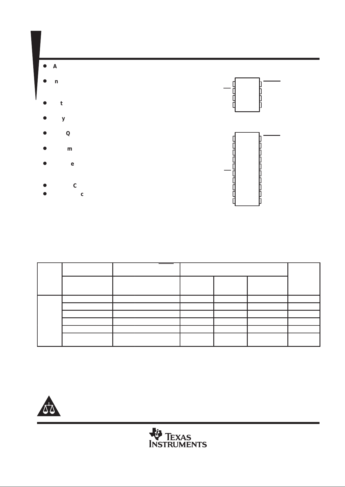
AVAILABLE OPTIONS
OUTPUT VOLTAGE
(V)
NEGATIVE-GOING RESET
THRESHOLD VOLTAGE (V)
PACKAGED DEVICES
T
J
MIN TYP MAX MIN TYP MAX
SMALL
OUTLINE
(D)
PLASTIC DIP
(P)
TSSOP
(PW)
CHIP FORM
(Y)
4.9 5 5.1 4.55 4.65 4.75 TPS7350QD TPS7350QP TPS7350QPW TPS7350Y
4.75 4.85 4.95 4.5 4.6 4.7 TPS7348QD TPS7348QP TPS7348QPW TPS7348Y
°
3.23 3.3 3.37 2.868 2.934 3 TPS7333QD TPS7333QP TPS7333QPW TPS7333Y
–
40°C to
125°C
2.94 3 3.06 2.58 2.64 2.7 TPS7330QD TPS7330QP TPS7330QPW TPS7330Y
125 C
2.425 2.5 2.575 2.23 2.32 2.39 TPS7325QD TPS7325QP TPS7325QPW TPS7325Y
Adjustable
1.2 V to 9.75 V
1.101 1.123 1.145 TPS7301QD TPS7301QP TPS7301QPW TPS7301Y
The D and PW packages are available taped and reeled. Add an R suffix to device type (e.g., TPS7350QDR). The TPS7301Q is programmable
using an external resistor divider (see application information). The chip form is tested at 25°C.
§
The TPS7325 has a tolerance of ±3% over the full temperature range.
¶
The TPS71xx and the TPS72xx are 500-mA and 250-mA output regulators respectively, of fering performance similar to that of the TPS73xx but
without the delayed-reset function. The TPS72xx devices are further differentiated by availability in 8-pin thin-shrink small-outline packages
(TSSOP) for applications requiring minimum package size.
Please be aware that an important notice concerning availability, standard warranty, and use in critical applications of
Texas Instruments semiconductor products and disclaimers thereto appears at the end of this data sheet.
Copyright 1999, Texas Instruments Incorporated
PRODUCTION DATA information is current as of publication date.
Products conform to specifications per the terms of Texas Instruments
standard warranty. Production processing does not necessarily include
testing of all parameters.
1
2
3
4
5
6
7
8
9
10
20
19
18
17
16
15
14
13
12
11
GND
GND
GND
NC
NC
EN
NC
IN
IN
IN
RESET
NC
NC
FB
‡
NC
SENSE
†
OUT
OUT
NC
NC
PW PACKAGE
(TOP VIEW)
NC – No internal connection
†
SENSE – Fixed voltage options only
(TPS7325, TPS7330, TPS7333, TPS7348, and TPS7350)
‡
FB – Adjustable version only (TPS7301)
1
2
3
4
8
7
6
5
GND
EN
IN
IN
RESET
SENSE†/FB
‡
OUT
OUT
D OR P PACKAGE
(TOP VIEW)
TPS7301Q, TPS7325Q, TPS7330Q, TPS7333Q, TPS7348Q, TPS7350Q
LOW-DROPOUT VOLTAGE REGULATORS
WITH INTEGRATED DELAYED RESET FUNCTION
SLVS124F – JUNE 1995 – REVISED JANUAR Y 1999
2
POST OFFICE BOX 655303 • DALLAS, TEXAS 75265
description (continued)
The RESET output of the TPS73xx initiates a reset in microcomputer and microprocessor systems in the event
of an undervoltage condition. An internal comparator in the TPS73xx monitors the output voltage of the regulator
to detect an undervoltage condition on the regulated output voltage.
If that occurs, the RESET output (open-drain NMOS) turns on, taking the RESET signal low . RESET stays low
for the duration of the undervoltage condition. Once the undervoltage condition ceases, a 200-ms (typ) time-out
begins. At the completion of the 200-ms delay, RESET
goes high.
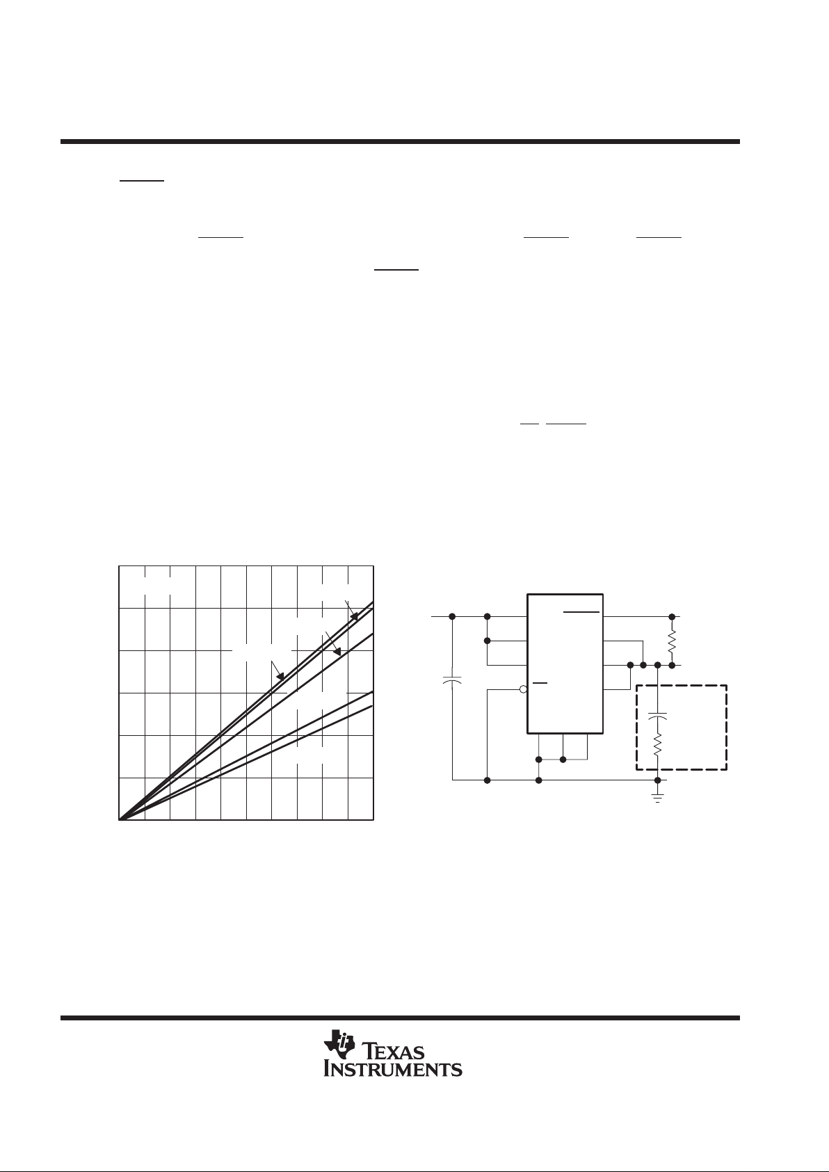
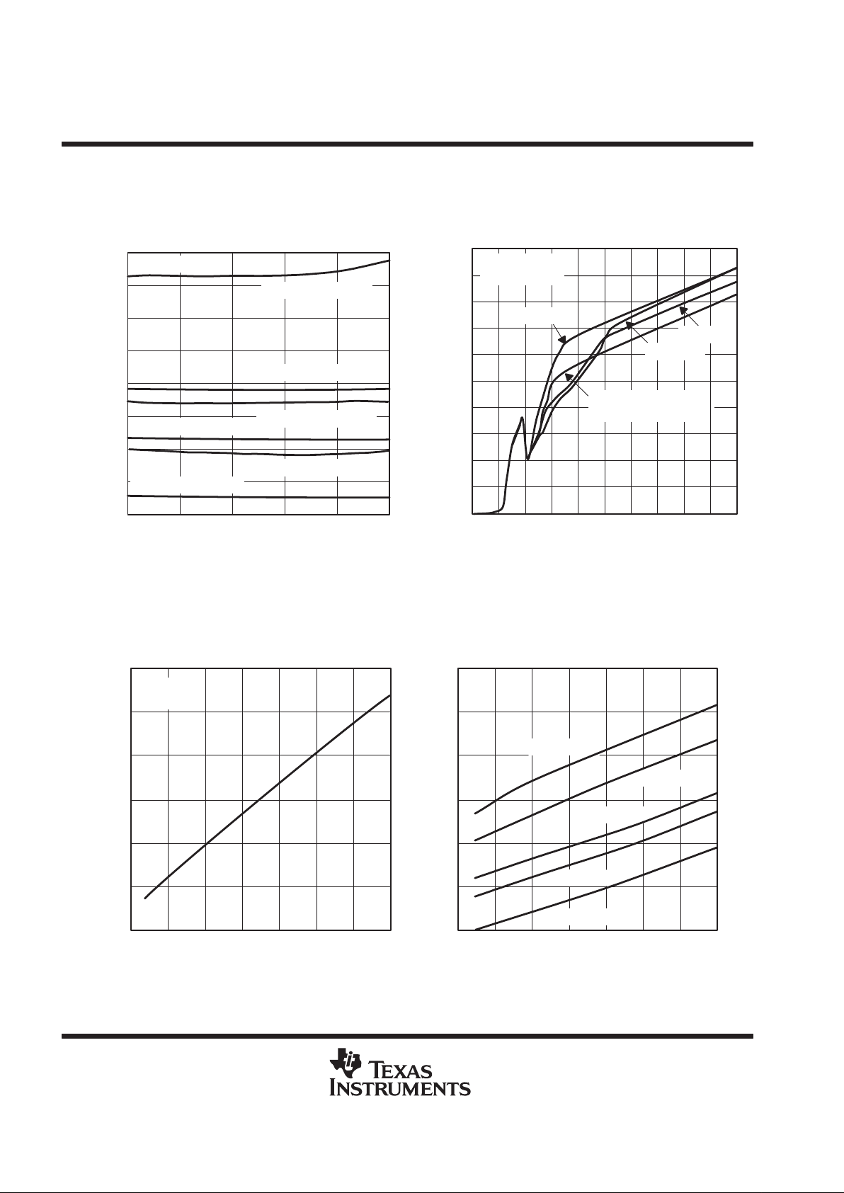
An order of magnitude reduction in dropout voltage and quiescent current over conventional LDO performance
is achieved by replacing the typical pnp pass transistor with a PMOS device.
Because the PMOS device behaves as a low-value resistor, the dropout voltage is very low (maximum of 35 mV
at an output current of 100 mA for the TPS7350) and is directly proportional to the output current (see Figure 1).
Additionally , since the PMOS pass element is a voltage-driven device, the quiescent current is low and remains
constant, independent of output loading (typically 340 µA over the full range of output current, 0 mA to 500 mA).
These two key specifications yield a significant improvement in operating life for battery-powered systems.
The LDO family also features a sleep mode; applying a logic high signal to EN (enable) shuts down the regulator,
reducing the quiescent current to 0.5 µA maximum at TJ = 25°C.
The TPS73xx is offered in 2.5-V , 3-V , 3.3-V , 4.85-V, and 5-V fixed-voltage versions and in an adjustable version
(programmable over the range of 1.2 V to 9.75 V). Output voltage tolerance is specified as a maximum of 2%
over line, load, and temperature ranges (3% for the 2.5 V and the adjustable version). The TPS73xx family is
available in PDIP (8 pin), SO (8 pin) and TSSOP (20 pin) packages. The TSSOP has a maximum height of
1.2 mm.
Figure 1. Dropout Voltage Versus Output Current
0.25
0.2
0.1
0.05
0
0.15
0 50 100 150 200 250 300
0.3
350 400 450 500
TA = 25°C
TPS7348
TPS7350
Dropout Voltage – V
IO – Output Current – mA
TPS7333
TPS7330
TPS7325
Figure 2. Typical Application Configuration
†
TPS7325, TPS7330, TPS7333, TPS7348, TPS7350 (fixed-voltage
options)
‡
Capacitor selection is nontrivial. See application information
section for details.
SENSE
RESET
OUT
OUT
9
8
6
10
IN
IN
IN
EN
GND
321
20
15
14
13
V
I
0.1 µF
To System
Reset
CSR = 1 Ω
V
O
10 µF
+
TPS73xxPW
†
C
O
‡
250 kΩ
TPS7301Q, TPS7325Q, TPS7330Q, TPS7333Q, TPS7348Q, TPS7350Q
LOW-DROPOUT VOLTAGE REGULATORS
WITH INTEGRATED DELAYED RESET FUNCTION
SLVS124F – JUNE 1995 – REVISED JANUAR Y 1999
3
POST OFFICE BOX 655303 • DALLAS, TEXAS 75265
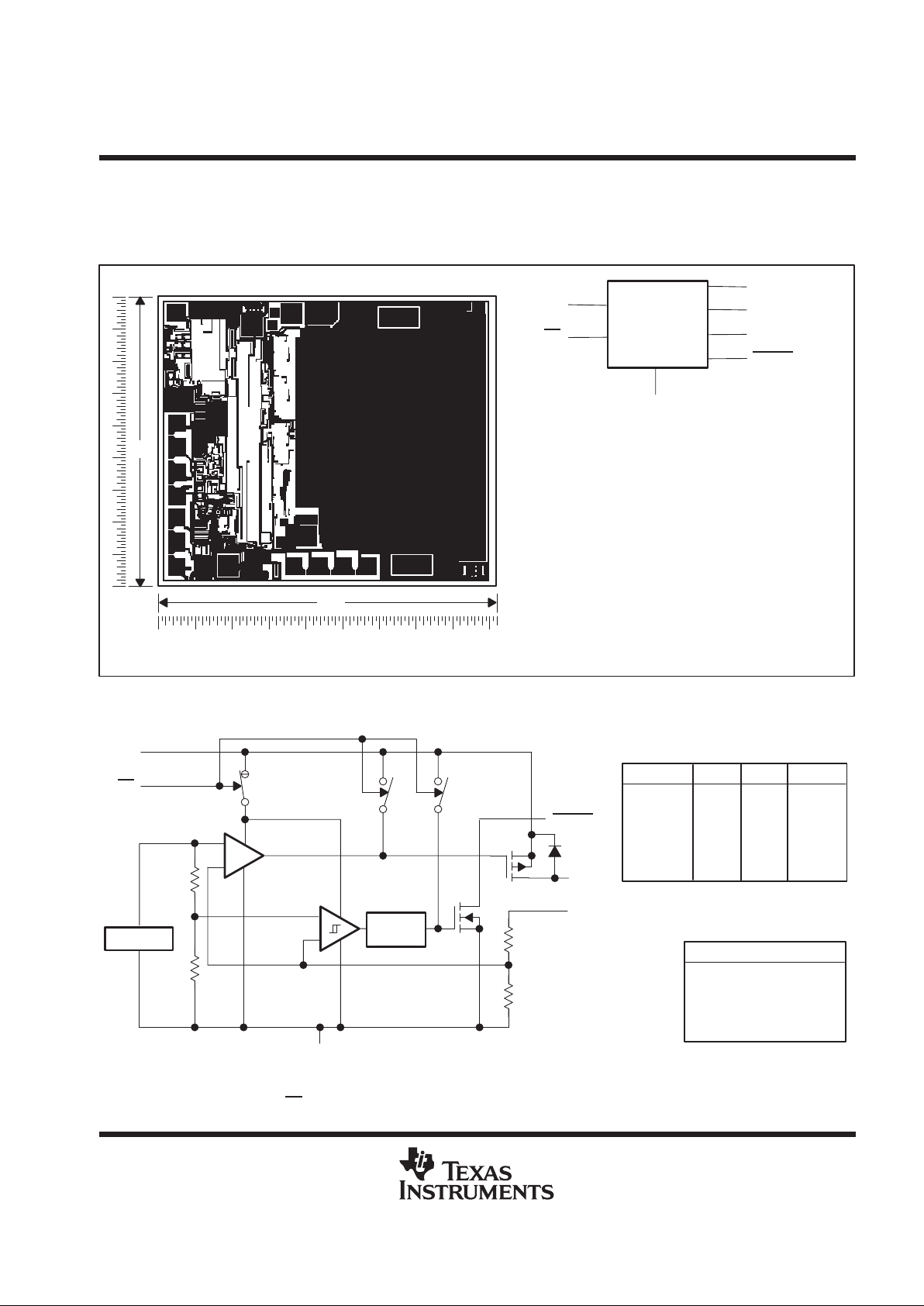
TPS73xxY chip information
These chips, when properly assembled, display characteristics similar to those of the TPS73xxQ. Thermal
compression or ultrasonic bonding may be used on the doped aluminum bonding pads. Chips may be mounted
with conductive epoxy or a gold-silicon preform.
(6)
(4)
(3)
(7)
(2)
(1)
GND
FB
‡
OUT
RESET
IN
EN
TPS73xx
80
92
CHIP THICKNESS: 15 TYPICAL
BONDING PADS: 4 × 4 MINIMUM
TJmax = 150°C
TOLERANCES ARE ±10%.
ALL DIMENSIONS ARE IN MILS.
†
SENSE – Fixed voltage options only (TPS7325, TPS7330,
TPS7333, TPS7348, and TPS7350)
‡
FB – Adjustable version only (TPS7301)
BONDING PAD ASSIGNMENTS
SENSE
†
(5)
NOTE A. For most applications, OUT and SENSE should
be tied together as close as possible to the device;
for other implementations, refer to SENSE-pin
connection discussion in the applications
information section of this data sheet.
(3)
(4)
(5)
(6)
(7)
(2)
(1)
functional block diagram
¶
_
+
V
ref
OUT
SENSE§/FB
EN
IN
GND
R1
R2
RESET
_
+
TPS7301
TPS7325
TPS7330
TPS7333
TPS7348
TPS7350
DEVICE
UNITR1 R2
0
260
358
420
726
756
∞
233
233
233
233
233
Ω
kΩ
kΩ
kΩ
kΩ
kΩ
RESISTOR DIVIDER OPTIONS
§
For most applications, SENSE should be externally connected to OUT as close as possible to the device. For other implementations, refer to
SENSE-pin connection discussion in applications information section.
¶
Switch positions are shown with EN
low (active).
NOTE A. Resistors are nominal values only.
Delayed
Reset
¶¶
MOS transistors
Bilpolar transistors
Diodes
Capacitors
Resistors
COMPONENT COUNT
464
41
4
17
76
TPS7301Q, TPS7325Q, TPS7330Q, TPS7333Q, TPS7348Q, TPS7350Q
LOW-DROPOUT VOLTAGE REGULATORS
WITH INTEGRATED DELAYED RESET FUNCTION
SLVS124F – JUNE 1995 – REVISED JANUAR Y 1999
4
POST OFFICE BOX 655303 • DALLAS, TEXAS 75265
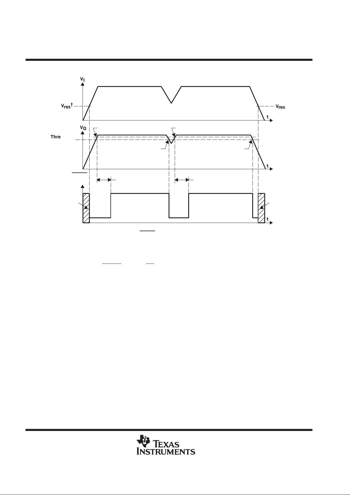
timing diagram
†
V
res
is the minimum input voltage for a valid RESET . The symbol V
res
is not currently listed within EIA or JEDEC standards
for semiconductor symbology.
V
I
V
res
†
V
res
t
t
t
V
O
Threshold
Voltage
RESET
Output
200 ms
Delay
200 ms
Delay
Output
Undefined
Output
Undefined
V
IT+
V
IT–
V
IT–
V
IT+
absolute maximum ratings over operating free-air temperature range (unless otherwise noted)
‡
Input voltage range
§
, VI, RESET, SENSE, EN –0.3 V to 11 V. . . . . . . . . . . . . . . . . . . . . . . . . . . . . . . . . . . . . . . .
Output current, IO 2 A. . . . . . . . . . . . . . . . . . . . . . . . . . . . . . . . . . . . . . . . . . . . . . . . . . . . . . . . . . . . . . . . . . . . . . . . . . .
Continuous total power dissipation See Dissipation Rating Tables 1 and 2. . . . . . . . . . . . . . . . . . . . . . . . . . . . .
Operating virtual junction temperature range, TJ –55°C to 150°C. . . . . . . . . . . . . . . . . . . . . . . . . . . . . . . . . . . . .
Storage temperature range, T
stg
–65°C to 150°C. . . . . . . . . . . . . . . . . . . . . . . . . . . . . . . . . . . . . . . . . . . . . . . . . . .
Lead temperature 1,6 mm (1/16 inch) from case for 10 seconds 260°C. . . . . . . . . . . . . . . . . . . . . . . . . . . . . . .
‡
Stresses beyond those listed under “absolute maximum ratings” may cause permanent damage to the device. These are stress ratings only, and
functional operation of the device at these or any other conditions beyond those indicated under “recommended operating conditions” is not
implied. Exposure to absolute-maximum-rated conditions for extended periods may affect device reliability.
§
All voltage values are with respect to network terminal ground.
TPS7301Q, TPS7325Q, TPS7330Q, TPS7333Q, TPS7348Q, TPS7350Q
LOW-DROPOUT VOLTAGE REGULATORS
WITH INTEGRATED DELAYED RESET FUNCTION
SLVS124F – JUNE 1995 – REVISED JANUAR Y 1999
5
POST OFFICE BOX 655303 • DALLAS, TEXAS 75265
DISSIPATION RATING TABLE 1 – FREE-AIR TEMPERATURE (SEE FIGURE 3)
T
≤ 25°C DERATING FACTOR T
= 70°C T
= 125°C
PACKAGE
A
POWER RATING ABOVE TA = 25°CAPOWER RATINGAPOWER RATING
D 725 mW 5.8 mW/°C 464 mW 145 mW
P 1 175 mW 9.4 mW/°C 752 mW 235 mW
PW
†
700 mW 5.6 mW/°C 448 mW 140 mW
DISSIPATION RA TING TABLE 2 – CASE TEMPERATURE (SEE FIGURE 4)
T
≤ 25°C DERATING FACTOR T
= 70°C T
= 125°C
PACKAGE
C
POWER RATING ABOVE TC = 25°CCPOWER RATINGCPOWER RATING
D 2188 mW 9.4 mW/°C 1765 mW 1248 mW
P 2738 mW 21.9 mW/°C 1752 mW 548 mW
PW
†
4025 mW 32.2 mW/°C 2576 mW 805 mW
†
Refer to Thermal Information section for detailed power dissipation considerations when using the
TSSOP package.
Figure 3
PW Package
R
θJA
= 178°C/W
1200
800
400
0
25 50 75 100
– Maximum Continuous Dissipation – mW
MAXIMUM CONTINUOUS DISSIPATION
vs
FREE-AIR TEMPERATURE
125 150
1400
1000
600
200
P
D
TA – Free-Air Temperature – °C
D Package
R
θJA
= 172°C/W
P Package
R
θJA
= 106°C/W
Figure 4
2400
1600
800
0
25 50 75 100
– Maximum Continuous Dissipation – mW
3200
4000
MAXIMUM CONTINUOUS DISSIPATION
vs
CASE TEMPERATURE
4800
125 150
4400
3600
2800
2000
1200
400
P
D
TC – Case Temperature – °C
D Package
R
θJC
= 57°C/W
P Package
R
θJC
= 46°C/W
PW Package
R
θJC
= 37°C/W
TPS7301Q, TPS7325Q, TPS7330Q, TPS7333Q, TPS7348Q, TPS7350Q
LOW-DROPOUT VOLTAGE REGULATORS
WITH INTEGRATED DELAYED RESET FUNCTION
SLVS124F – JUNE 1995 – REVISED JANUAR Y 1999
6
POST OFFICE BOX 655303 • DALLAS, TEXAS 75265
recommended operating conditions
MIN MAX UNIT
TPS7301Q 2.47 10
TPS7325Q 3.1 10
V
p
TPS7330Q 3.5 10 V
Input voltage, V
I
†
TPS7333Q 3.77 10
TPS7348Q 5.2 10
V
TPS7350Q 5.33 10
High-level input voltage at EN, V
IH
2 V
Low-level input voltage at EN, V
IL
0.5 V
Output current range, I
O
0 500 mA
Operating virtual junction temperature range, T
J
–40 125 °C
†
Minimum input voltage defined in the recommended operating conditions is the maximum specified output voltage plus dropout voltage, VDO,
at the maximum specified load range. Since dropout voltage is a function of output current, the usable range can be extended for lighter loads.
To calculate the minimum input voltage for the maximum load current used in a given application, use the following equation:
V
I(min)
+
V
O(max)
)
V
DO(max load)
Because the TPS7301 is programmable, r
DS(on)
should be used to calculate VDO before applying the above equation. The equation for calculating
VDO from r
DS(on)
is given in Note 2 in the TPS7301 electrical characteristics table. The minimum value of 2.97 V is the absolute lower limit for
the recommended input voltage range for the TPS7301.
TPS7301Q, TPS7325Q, TPS7330Q, TPS7333Q, TPS7348Q, TPS7350Q
LOW-DROPOUT VOLTAGE REGULATORS
WITH INTEGRATED DELAYED RESET FUNCTION
SLVS124F – JUNE 1995 – REVISED JANUAR Y 1999
7
POST OFFICE BOX 655303 • DALLAS, TEXAS 75265
electrical characteristics at IO = 10 mA, EN = 0 V, Co = 4.7 µF (CSR‡ = 1 Ω), SENSE/FB shorted to
OUT (unless otherwise noted)
PARAMETER
TEST CONDITIONS
§
T
J
MIN TYP MAX
UNIT
EN ≤ 0.5 V, V
= V
+ 1 V
,
25°C 340 400
Ground current (active mode)
EN ≤ 0.5 V,
V
I
V
O
+ 1
V,
0 mA ≤ IO ≤ 500 mA
–40°C to 125°C 550
µ
A
p
25°C 0.01 0.5
Input current (standby mode)
EN
=
V
I
,
2.7 V ≤ V
I
≤ 10
V
–40°C to 125°C 2
µ
A
p
25°C 1.2 2
Output current limit
V
O
= 0 V,
V
I
= 10
V
–40°C to 125°C 2
A
Pass-element leakage current in standby
25°C 0.01 0.5
gy
mode
EN
=
V
I
,
2.7 V ≤ V
I
≤ 10 V
–40°C to 125°C 1
µ
A
25°C 0.02 0.5
RESET leak
age curren
t
N
ormal operation,V at
RESET
= 10
V
–40°C to 125°C 0.5
µ
A
Output voltage temperature coefficient –40°C to 125°C 61 75 ppm/°C
Thermal shutdown junction temperature 165 °C
2.5 V ≤ VI ≤ 6 V
°
°
2
EN logic high (standb
y mode
)
6 V ≤ VI ≤ 10 V
–
40°C to 125°C
2.7
V
25°C 0.5
EN logic l
ow (active mode
)
2.7 V ≤ V
I
≤ 10 V
–40°C to 125°C 0.5
V
EN hysteresis voltage 25°C 50 mV
25°C –0.5 0.001 0.5
EN i
nput curren
t
0 V ≤ V
I
≤ 10 V
–40°C to 125°C –0.5 0.5
µ
A
p
25°C 2.05 2.5
Minimum V
I
for active pass element
–40°C to 125°C 2.5
V
25°C 1 1.5
Mini
mum
V
I
f
or va
lid RESET
I
O(RESET)
= –
300 µA
–40°C to 125°C 1.9
V
‡
CSR (compensation series resistance) refers to the total series resistance, including the equivalent series resistance (ESR) of the capacitor, any
series resistance added externally , and PWB trace resistance to Co.
§
Pulse-testing techniques are used to maintain virtual junction temperature as close as possible to ambient temperature; thermal effects must
be taken into account separately.
TPS7301Q, TPS7325Q, TPS7330Q, TPS7333Q, TPS7348Q, TPS7350Q
LOW-DROPOUT VOLTAGE REGULATORS
WITH INTEGRATED DELAYED RESET FUNCTION
SLVS124F – JUNE 1995 – REVISED JANUAR Y 1999
8
POST OFFICE BOX 655303 • DALLAS, TEXAS 75265
TPS7301Q electrical characteristics at IO = 10 mA, V
I
= 3.5 V , EN = 0 V, Co = 4.7 µF (CSR† = 1 Ω), FB
shorted to OUT at device leads (unless otherwise noted)
PARAMETER
TEST CONDITIONS
‡
T
J
MIN TYP MAX
UNIT
25°C 1.182 V
Reference voltage (measured at FB)
2.5 V ≤ VI ≤ 10 V,
See Note 1
5 mA ≤ IO ≤ 500 mA,
–40°C to 125°C 1.147 1.217 V
Reference voltage temperature
coefficient
–40°C to 125°C 61 75 ppm/°C
25°C 0.7 1
V
I
= 2.4 V,
50 µA ≤ I
O
≤
150 mA
–40°C to 125°C 1
25°C 0.83 1.3
Pass-element series resistance
V
I
=
2.4 V
,
150 mA ≤ I
O
≤ 500 mA
–40°C to 125°C 1.3
(See Note 2)
25°C 0.52 0.85
Ω
V
I
= 2.9 V,
50 µA ≤ I
O
≤
500 mA
–40°C to 125°C 0.85
VI = 3.9 V, 50 µA ≤ IO ≤ 500 mA 25 °C 0.32
VI = 5.9 V, 50 µA ≤ IO ≤ 500 mA 25 °C 0.23
p
V
= 2.5 V to 10 V, 50 µA ≤ I
≤ 500 mA,
25°C 3 18
Input regulation
I
,
See Note 1
µ
O
,
–40°C to 125°C 25
mV
2.5 V ≤ V
≤ 10 V, I
= 5 mA to 500 mA,
25°C 5 14
p
I
,
See Note 1
O
,
–40°C to 125°C 25
mV
Output regulation
2.5 V ≤ V
≤ 10 V, I
= 50 µA to 500 mA,
25°C 7 22
I
,
See Note 1
O
µ ,
–40°C to 125°C 54
mV
25°C 48 59
pp
I
O
=
50 µA
–40°C to 125°C 44
Ripple rejection
f
=
120 H
z
I
= 500 mA,
25°C 45 54
dB
O
,
See Note 1
–40°C to 125°C 44
Output noise-spectral density f = 120 Hz 25°C 2
µV/√Hz
Co = 4.7 µF 25°C 95
Output noise voltage 10 Hz ≤ f ≤ 100 kHz
Co = 10 µF 25°C 89
µVrms
Co = 100 µF 25°C 74
RESET trip-threshold voltage
§
V
O(FB)
decreasing –40°C to 125°C 1.101 1.145 V
RESET hysteresis voltage
§
Measured at V
O(FB)
25°C 12 mV
p
25°C 0.1 0.4
RESET
output low voltage
§
V
I
= 2.13 V,
I
O(RESET)
=
400 µA
–40°C to 125°C 0.4
V
p
25°C –10 0.1 10
FB input current
–40°C to 125°C –20 20
nA
†
CSR refers to the total series resistance, including the ESR of the capacitor, any series resistance added externally , and PWB trace resistance
to Co.
‡
Pulse-testing techniques are used to maintain virtual junction temperature as close as possible to ambient temperature; thermal effects must
be taken into account separately.
§
Output voltage programmed to 2.5 V with closed-loop configuration (see application information).
NOTES: 1. When VI < 2.9 V and IO > 150 mA simultaneously, pass element r
DS(on)
increases (see Figure 33) to a point where the resulting
dropout voltage prevents the regulator from maintaining the specified tolerance range.
2. To calculate dropout voltage, use equation: VDO = IO
⋅ r
DS(on)
r
DS(on)
is a function of both output current and input voltage. This parametric table lists r
DS(on)
for VI = 2.4 V, 2.9 V, 3.9 V, and
5.9 V , which corresponds to dropout conditions for programmed output voltages of 2.5 V, 3 V, 4 V, and 6 V respectively . For other
programmed values, refer to Figure 33.
TPS7301Q, TPS7325Q, TPS7330Q, TPS7333Q, TPS7348Q, TPS7350Q
LOW-DROPOUT VOLTAGE REGULATORS
WITH INTEGRATED DELAYED RESET FUNCTION
SLVS124F – JUNE 1995 – REVISED JANUAR Y 1999
9
POST OFFICE BOX 655303 • DALLAS, TEXAS 75265
TPS7325Q electrical characteristics at IO = 10 mA, V
I
= 3.5 V , EN = 0 V, Co = 10 µF (CSR† = 1 Ω), SENSE
shorted to OUT (unless otherwise noted)
PARAMETER
TEST CONDITIONS
‡
T
J
MIN TYP MAX
UNIT
p
25°C 2.45 2.5 2.55
Output voltage
3.5 V ≤ VI ≤ 10 V, 5 mA ≤ IO ≤ 500 mA –40°C to 125°C 2.425 2.575
V
25°C 5
I
O
= 10 mA,
V
I
= 2.97
V
–40°C to 125°C 14
25°C 50 80
D
ropout voltage
§
I
O
=
100 mA
,
V
I
=
2.97 V
–40°C to 125°C 150
mV
25°C 270 400
I
O
=
500 mA
,
V
I
= 2.97
V
–40°C to 125°C 600
(2.97 V – V
)/I
, V
= 2.97 V ,
25°C 0.5 0.7
Pass-element series resistance
§
(
O)O
,
IO = 500 mA
I
,
–40°C to 125°C 1.4
Ω
p
25°C 6 20
Input regulation
V
I
=
3.5 V to 10 V
,
50 µA ≤ I
O
≤ 500 mA
–40°C to 125°C 25
mV
25°C 20 32
p
I
O
=
5 mA to 500 mA
,3.5 V ≤
V
I
≤ 10 V
–40°C to 125°C 50
mV
Output regulation
25°C 28 60
I
O
= 50 µA to
500 mA
,3.5 V ≤
V
I
≤ 10
V
–40°C to 125°C 100
mV
25°C 50 53
pp
I
O
=
50 µA
–40°C to 125°C 49
Ripple rejection
f
=
120 H
z
25°C 49 53
dB
I
O
=
500 mA
–40°C to 125°C 32
Output noise-spectral density f = 120 Hz 25°C 2
µV/√Hz
Co = 4.7 µF
25°C 274
Output noise voltage 10 Hz ≤ f ≤ 100 kHz
Co = 10 µF
25°C 228
µVrms
Co = 100 µF
25°C 159
RESET trip-threshold voltage
VO decreasing –40°C to 125°C 2.23 2.32 2.39 V
p
25°C 0.14 0.4
RESET output low voltage
V
I
=
2.1 V
,
I
O(RESET)
= –
0.8 mA
–40°C to 125°C 0.4
V
†
CSR refers to the total series resistance, including the ESR of the capacitor, any series resistance added externally , and PWB trace resistance
to Co.
‡
Pulse-testing techniques are used to maintain virtual junction temperature as close as possible to ambient temperature; thermal effects must
be taken into account separately.
§
Dropout test and pass-element series resistance test are not production tested. Test method requires SENSE terminal to be disconnected from
output voltage.
TPS7301Q, TPS7325Q, TPS7330Q, TPS7333Q, TPS7348Q, TPS7350Q
LOW-DROPOUT VOLTAGE REGULATORS
WITH INTEGRATED DELAYED RESET FUNCTION
SLVS124F – JUNE 1995 – REVISED JANUAR Y 1999
10
POST OFFICE BOX 655303 • DALLAS, TEXAS 75265
TPS7330Q electrical characteristics at IO = 10 mA, V
I
= 4 V , EN = 0 V , Co = 4.7 µF (CSR† = 1 Ω), SENSE
shorted to OUT (unless otherwise noted)
PARAMETER
TEST CONDITIONS
‡
T
J
MIN TYP MAX
UNIT
p
25°C 3
Output voltage
4 V ≤ VI ≤ 10 V, 5 mA ≤ IO ≤ 500 mA –40°C to 125°C 2.94 3.06
V
25°C 5.2 7
I
O
= 10 mA,
V
I
= 2.94
V
–40°C to 125°C 10
25°C 52 75
D
ropout voltage
I
O
=
100 mA
,
V
I
=
2.94 V
–40°C to 125°C 100
mV
25°C 267 450
I
O
=
500 mA
,
V
I
= 2.94
V
–40°C to 125°C 500
(2.94 V – V
)/I
, V
= 2.94 V ,
25°C 0.5 0.7
Pass-element series resistance
(
O)O
,
IO = 500 mA
I
,
–40°C to 125°C 1
Ω
p
25°C 6 23
Input regulation
V
I
=
4 V to 10 V
,
50 µA ≤ I
O
≤ 500 mA
–40°C to 125°C 29
mV
25°C 20 32
p
I
O
=
5 mA to 500 mA
,4 V ≤
V
I
≤ 10 V
–40°C to 125°C 60
mV
Output regulation
25°C 28 60
I
O
= 50 µA to
500 mA
,4 V ≤
V
I
≤ 10
V
–40°C to 125°C 120
mV
25°C 43 53
pp
I
O
=
50 µA
–40°C to 125°C 40
Ripple rejection
f
=
120 H
z
25°C 39 53
dB
I
O
=
500 mA
–40°C to 125°C 36
Output noise-spectral density f = 120 Hz 25°C 2
µV/√Hz
Co = 4.7 µF
25°C 274
Output noise voltage 10 Hz ≤ f ≤ 100 kHz
Co = 10 µF
25°C 228
µVrms
Co = 100 µF
25°C 159
RESET trip-threshold voltage
VO decreasing –40°C to 125°C 2.58 2.64 2.7 V
p
25°C 0.14 0.4
RESET output low voltage
V
I
=
2.6 V
,
I
O(RESET)
= –
0.8 mA
–40°C to 125°C 0.4
V
†
CSR refers to the total series resistance, including the ESR of the capacitor, any series resistance added externally , and PWB trace resistance
to Co.
‡
Pulse-testing techniques are used to maintain virtual junction temperature as close as possible to ambient temperature; thermal effects must
be taken into account separately.
TPS7301Q, TPS7325Q, TPS7330Q, TPS7333Q, TPS7348Q, TPS7350Q
LOW-DROPOUT VOLTAGE REGULATORS
WITH INTEGRATED DELAYED RESET FUNCTION
SLVS124F – JUNE 1995 – REVISED JANUAR Y 1999
11
POST OFFICE BOX 655303 • DALLAS, TEXAS 75265
TPS7333Q electrical characteristics at IO = 10 mA, V
I
= 4.3 V, EN = 0 V, Co = 4.7 µF (CSR† = 1 Ω),
SENSE shorted to OUT (unless otherwise noted)
PARAMETER
TEST CONDITIONS
‡
T
J
MIN TYP MAX
UNIT
p
25°C 3.3
Output voltage
4.3 V ≤ VI ≤ 10 V, 5 mA ≤ IO ≤ 500 mA –40°C to 125°C 3.23 3.37
V
25°C 4.5 7
I
O
= 10 mA,
V
I
= 3.23
V
–40°C to 125°C 8
25°C 44 60
D
ropout voltage
I
O
=
100 mA
,
V
I
=
3.23 V
–40°C to 125°C 80
mV
25°C 235 300
I
O
=
500 mA
,
V
I
= 3.23
V
–40°C to 125°C 400
(3.23 V – V
)/I
, V
= 3.23 V ,
25°C 0.44 0.6
Pass-element series resistance
(
O)O
,
IO = 500 mA
I
,
–40°C to 125°C 0.8
Ω
p
25°C 6 23
Input regulation
V
I
=
4.3 V to 10 V
,
50 µA ≤ I
O
≤ 500 mA
–40°C to 125°C 29
mV
25°C 21 38
p
I
O
=
5 mA to 500 mA, 4.3 V ≤ V
I
≤ 10 V
–40°C to 125°C 75
mV
Output regulation
25°C 31 60
I
O
= 50 µA to
500 mA, 4.3 V ≤ V
I
≤ 10
V
–40°C to 125°C 120
mV
25°C 43 51
pp
I
O
=
50 µA
–40°C to 125°C 40
Ripple rejection
f
=
120 H
z
25°C 39 49
dB
I
O
=
500 mA
–40°C to 125°C 36
Output noise-spectral density f = 120 Hz 25°C 2
µV/√Hz
Co = 4.7 µF
25°C 274
Output noise voltage 10 Hz ≤ f ≤ 100 kHz
Co = 10 µF
25°C 228
µVrms
Co = 100 µF
25°C 159
RESET trip-threshold voltage
VO decreasing –40°C to 125°C 2.868 V
RESET hysteresis voltage
25°C 18 mV
p
25°C 0.17 0.4
RESET output low voltage
V
I
= 2.8 V,
I
O(RESET)
= –1
mA
–40°C to 125°C 0.4
V
†
CSR refers to the total series resistance, including the ESR of the capacitor, any series resistance added externally , and PWB trace resistance
to Co.
‡
Pulse-testing techniques are used to maintain virtual junction temperature as close as possible to ambient temperature; thermal effects must
be taken into account separately.
TPS7301Q, TPS7325Q, TPS7330Q, TPS7333Q, TPS7348Q, TPS7350Q
LOW-DROPOUT VOLTAGE REGULATORS
WITH INTEGRATED DELAYED RESET FUNCTION
SLVS124F – JUNE 1995 – REVISED JANUAR Y 1999
12
POST OFFICE BOX 655303 • DALLAS, TEXAS 75265
TPS7348Q electrical characteristics at IO = 10 mA, V
I
= 5.85 V, EN = 0 V, Co = 4.7 µF (CSR† = 1 Ω),
SENSE shorted to OUT (unless otherwise noted)
PARAMETER
TEST CONDITIONS
‡
T
J
MIN TYP MAX
UNIT
p
25°C 4.85
Output voltage
5.85 V ≤ VI ≤ 10 V, 5 mA ≤ IO ≤ 500 mA –40°C to 125°C 4.75 4.95
V
25°C 2.9 6
I
O
= 10 mA,
V
I
= 4.75
V
–40°C to 125°C 8
25°C 28 37
D
ropout voltage
I
O
=
100 mA
,
V
I
=
4.75 V
–40°C to 125°C 54
mV
25°C 150 180
I
O
=
500 mA
,
V
I
= 4.75
V
–40°C to 125°C 250
(4.75 V – V
)/I
, V
= 4.75 V ,
25°C 0.28 0.37
Pass-element series resistance
(
O)O
,
IO = 500 mA
I
,
–40°C to 125°C 0.52
Ω
p
25°C 9 35
Input regulation
V
I
=
5.85 V to 10 V
,
50 µA ≤ I
O
≤ 500 mA
–40°C to 125°C 37
mV
25°C 28 42
p
I
O
=
5 mA to 500 mA, 5.85 V ≤ V
I
≤ 10 V
–40°C to 125°C 80
mV
Output regulation
25°C 42 65
I
O
= 50 µA to
500 mA, 5.85 V ≤ V
I
≤ 10
V
–40°C to 125°C 130
mV
25°C 42 53
pp
I
O
=
50 µA
–40°C to 125°C 39
Ripple rejection
f
=
120 H
z
25°C 39 50
dB
I
O
=
500 mA
–40°C to 125°C 35
Output noise-spectral density f = 120 Hz 25°C 2 µV/√Hz
Co = 4.7 µF
25°C 410
Output noise voltage 10 Hz ≤ f ≤ 100 kHz
Co = 10 µF
25°C 328
µVrms
Co = 100 µF
25°C 212
RESET trip-threshold voltage
VO decreasing –40°C to 125°C 4.5 4.7 V
RESET hysteresis voltage
25°C 26 mV
p
25°C 0.2 0.4
RESET output low voltage
I
O(RESET)
= –
1.2 mA,V
I
=
4.12 V
–40°C to 125°C 0.4
V
†
CSR refers to the total series resistance, including the ESR of the capacitor, any series resistance added externally , and PWB trace resistance
to Co.
‡
Pulse-testing techniques are used to maintain virtual junction temperature as close as possible to ambient temperature; thermal effects must
be taken into account separately.
TPS7301Q, TPS7325Q, TPS7330Q, TPS7333Q, TPS7348Q, TPS7350Q
LOW-DROPOUT VOLTAGE REGULATORS
WITH INTEGRATED DELAYED RESET FUNCTION
SLVS124F – JUNE 1995 – REVISED JANUAR Y 1999
13
POST OFFICE BOX 655303 • DALLAS, TEXAS 75265
TPS7350Q electrical characteristics at IO = 10 mA, V
I
= 6 V , EN = 0 V , Co = 4.7 µF (CSR† = 1 Ω), SENSE
shorted to OUT (unless otherwise noted)
PARAMETER
TEST CONDITIONS
‡
T
J
MIN TYP MAX
UNIT
p
25°C 5
Output voltage
6 V ≤ VI ≤ 10 V, 5 mA ≤ IO ≤ 500 mA –40°C to 125°C 4.9 5.1
V
25°C 2.9 6
I
O
= 10 mA,
V
I
= 4.88
V
–40°C to 125°C 8
25°C 27 35
D
ropout voltage
I
O
=
100 mA
,
V
I
=
4.88 V
–40°C to 125°C 50
mV
25°C 146 170
I
O
=
500 mA
,
V
I
= 4.88
V
–40°C to 125°C 230
(4.88 V – V
)/I
, V
= 4.88 V ,
25°C 0.27 0.35
Pass-element series resistance
(
O)O
,
IO = 500 mA
I
,
–40°C to 125°C 0.5
Ω
p
25°C 4 25
Input regulation
V
I
=
6 V to 10 V
,
50 µA ≤ I
O
≤ 500 mA
–40°C to 125°C 45
mV
25°C 30 45
p
I
O
=
5 mA to 500 mA
,6 V ≤
V
I
≤ 10 V
–40°C to 125°C 86
mV
Output regulation
25°C 45 65
I
O
= 50 µA to
500 mA
,6 V ≤
V
I
≤ 10
V
–40°C to 125°C 140
mV
25°C 43 53
pp
I
O
=
50 µA
–40°C to 125°C 38
Ripple rejection
f
=
120 H
z
25°C 41 51
dB
I
O
=
500 mA
–40°C to 125°C 36
Output noise-spectral density f = 120 Hz 25°C 2
µV/√Hz
Co = 4.7 µF
25°C 430
Output noise voltage 10 Hz ≤ f ≤ 100 kHz
Co = 10 µF
25°C 345
µVrms
Co = 100 µF
25°C 220
RESET trip-threshold voltage
VO decreasing –40°C to 125°C 4.55 4.75 V
RESET hysteresis voltage
25°C 28 mV
p
25°C 0.15 0.4
RESET output low voltage
I
O(RESET)
= –1.2 mA,
V
I
= 4.25
V
–40°C to 125°C 0.4
V
†
CSR refers to the total series resistance, including the ESR of the capacitor, any series resistance added externally , and PWB trace resistance
to Co.
‡
Pulse-testing techniques are used to maintain virtual junction temperature as close as possible to ambient temperature; thermal effects must
be taken into account separately.

TPS7301Q, TPS7325Q, TPS7330Q, TPS7333Q, TPS7348Q, TPS7350Q
LOW-DROPOUT VOLTAGE REGULATORS
WITH INTEGRATED DELAYED RESET FUNCTION
SLVS124F – JUNE 1995 – REVISED JANUAR Y 1999
14
POST OFFICE BOX 655303 • DALLAS, TEXAS 75265
switching characteristics
PARAMETER TEST CONDITIONS
T
TPS7301Q, TPS7333Q
TPS7348Q, TPS7350Q
UNIT
J
MIN TYP MAX
25°C 140 200 260
RESET ti
me-out delay
See Figure 5
–40°C to 125°C 100 300
ms
electrical characteristics at IO = 10 mA, EN = 0 V, Co = 4.7 µF (CSR† = 1 Ω), TJ = 25°C, SENSE/FB
shorted to OUT (unless otherwise noted)
PARAMETER
TEST CONDITIONS
‡
TPS7301Y, TPS7333Y
TPS7348Y, TPS7350Y
UNIT
MIN TYP MAX
Ground current (active mode)
EN ≤ 0.5 V,
0 mA ≤ IO ≤ 500 mA
VI = VO + 1 V,
340 µA
Input current (standby mode)
EN = VI, 2.7 V ≤ VI ≤ 10 V
0.01 µA
Output current limit VO = 0 V, VI = 10 V 1.2 A
Pass-element leakage current in standby mode
EN = VI, 2.7 V ≤ VI ≤ 10 V
0.01 µA
RESET leakage current
Normal operation, V at RESET = 10 V
0.02 µA
Thermal shutdown junction temperature 165 °C
EN logic low (active mode)
2.7 V ≤ VI ≤ 10 V 0.5 V
EN hysteresis voltage 50 mV
EN input current
0 V ≤ VI ≤ 10 V 0.001 µA
Minimum VI for active pass element 2.05 V
Minimum VI for valid RESET
I
O(RESET)
= –300 µA 1 V
†
CSR (compensation series resistance) refers to the total series resistance, including the equivalent series resistance (ESR) of the capacitor, any
series resistance added externally , and PWB trace resistance to Co.
‡
Pulse-testing techniques are used to maintain virtual junction temperature as close as possible to ambient temperature; thermal effects must
be taken into account separately.

TPS7301Q, TPS7325Q, TPS7330Q, TPS7333Q, TPS7348Q, TPS7350Q
LOW-DROPOUT VOLTAGE REGULATORS
WITH INTEGRATED DELAYED RESET FUNCTION
SLVS124F – JUNE 1995 – REVISED JANUAR Y 1999
15
POST OFFICE BOX 655303 • DALLAS, TEXAS 75265
TPS7301Y electrical characteristics at IO = 10 mA, V
I
= 3.5 V, EN = 0 V, Co = 4.7 µF (CSR† = 1 Ω),
T
J
= 25°C, FB shorted to OUT at device leads (unless otherwise noted)
PARAMETER
TEST CONDITIONS
‡
MIN TYP MAX
UNIT
Reference voltage (measured at FB) 1.182 V
VI = 2.4 V, 50 µA ≤ IO ≤ 150 mA 0.7
VI = 2.4 V, 150 mA ≤ IO ≤ 500 mA 0.83
Pass-element series resistance (See Note 2)
VI = 2.9 V, 50 µA ≤ IO ≤ 500 mA 0.52
Ω
VI = 3.9 V, 50 µA ≤ IO ≤ 500 mA 0.32
VI = 5.9 V, 50 µA ≤ IO ≤ 500 mA 0.23
Input regulation
VI = 2.5 V to 10 V,
See Note 1
50 µA ≤ IO ≤ 500 mA,
3 mV
p
2.5 V ≤ VI ≤ 10 V,
See Note 1
IO = 5 mA to 500 mA,
5 mV
Output regulation
2.5 V ≤ VI ≤ 10 V,
See Note 1
IO = 50 µA to 500 mA,
7 mV
IO = 50 µA 59
Ripple rejection f = 120 Hz
IO = 500 mA,
See Note 1
54
dB
Output noise-spectral density f = 120 Hz 2
µV/√Hz
Co = 4.7 µF 95
Output noise voltage 10 Hz ≤ f ≤ 100 kHz
Co = 10 µF 89
µVrms
Co = 100 µF 74
RESET hysteresis voltage
§
Measured at V
O(FB)
12 mV
RESET output low voltage
§
VI = 2.13 V , I
O(RESET)
= 400 µA 0.1 V
FB input current 0.1 nA
†
CSR refers to the total series resistance, including the ESR of the capacitor, any series resistance added externally , and PWB trace resistance
to Co.
‡
Pulse-testing techniques are used to maintain virtual junction temperature as close as possible to ambient temperature; thermal effects must
be taken into account separately.
§
Output voltage programmed to 2.5 V with closed-loop configuration (see application information).
NOTES: 1. When VI < 2.9 V and IO > 150 mA simultaneously, pass element r
DS(on)
increases (see Figure 33) to a point where the resulting
dropout voltage prevents the regulator from maintaining the specified tolerance range.
2. To calculate dropout voltage, use equation: VDO = IO
⋅ r
DS(on)
r
DS(on)
is a function of both output current and input voltage. The parametric table lists r
DS(on)
for VI = 2.4 V, 2.9 V, 3.9 V, and
5.9 V , which corresponds to dropout conditions for programmed output voltages of 2.5 V, 3 V, 4 V, and 6 V respectively . For other
programmed values, refer to Figure 33.

TPS7301Q, TPS7325Q, TPS7330Q, TPS7333Q, TPS7348Q, TPS7350Q
LOW-DROPOUT VOLTAGE REGULATORS
WITH INTEGRATED DELAYED RESET FUNCTION
SLVS124F – JUNE 1995 – REVISED JANUAR Y 1999
16
POST OFFICE BOX 655303 • DALLAS, TEXAS 75265
TPS7325Y electrical characteristics at IO = 10 mA, V
I
= 3.5 V, EN = 0 V, Co = 10 µF (CSR† = 1 Ω),
T
J
= 25°C, SENSE shorted to OUT (unless otherwise noted)
PARAMETER
TEST CONDITIONS
‡
MIN TYP MAX
UNIT
Output voltage 2.5 V
IO = 10 mA, VI = 2.97 V 5
Dropout voltage
§
IO = 100 mA, VI = 2.97 V 50
mV
IO = 500 mA, VI = 2.97 V 270
Pass-element series resistance
§
(2.97 V – VO)/IO,
IO = 500 mA
VI = 2.97 V ,
0.5 Ω
Input regulation VI = 3.5 V to 10 V, 50 µA ≤ IO ≤ 500 mA 6 mV
p
IO = 5 mA to 500 mA, 3.5 V ≤ VI ≤ 10 V 20 mV
Output regulation
IO = 50 µA to 500 mA, 3.5 V ≤ VI ≤ 10 V 28 mV
pp
IO = 50 µA 53
Ripple rejection
f
=
120 H
z
IO = 500 mA 53
dB
Output noise-spectral density f = 120 Hz 2
µV/√Hz
Co = 4.7 µF
274
Output noise voltage 10 Hz ≤ f ≤ 100 kHz
Co = 10 µF
228
µVrms
Co = 100 µF
159
RESET output low voltage
VI = 2.1 V, I
O(RESET)
= –0.8 mA 0.14 V
†
CSR refers to the total series resistance, including the ESR of the capacitor, any series resistance added externally , and PWB trace resistance
to Co.
‡
Pulse-testing techniques are used to maintain virtual junction temperature as close as possible to ambient temperature; thermal effects must
be taken into account separately.
§
Dropout test and pass-element series resistance test are not production tested. Test method requires SENSE terminal to be disconnected from
output voltage.

TPS7301Q, TPS7325Q, TPS7330Q, TPS7333Q, TPS7348Q, TPS7350Q
LOW-DROPOUT VOLTAGE REGULATORS
WITH INTEGRATED DELAYED RESET FUNCTION
SLVS124F – JUNE 1995 – REVISED JANUAR Y 1999
17
POST OFFICE BOX 655303 • DALLAS, TEXAS 75265
TPS7330Y electrical characteristics at IO = 10 mA, V
I
= 4 V, EN = 0 V, Co = 4.7 µF (CSR† = 1 Ω),
T
J
= 25°C, SENSE shorted to OUT (unless otherwise noted)
PARAMETER
TEST CONDITIONS
‡
MIN TYP MAX
UNIT
Output voltage 3 V
IO = 10 mA, VI = 2.94 V 5.2
Dropout voltage
IO = 100 mA, VI = 2.94 V 52
mV
IO = 500 mA, VI = 2.94 V 267
Pass-element series resistance
(2.94 V – VO)/IO,
IO = 500 mA
VI = 2.94 V ,
0.5 Ω
Input regulation VI = 4 V to 10 V, 50 µA ≤ IO ≤ 500 mA 6 mV
p
IO = 5 mA to 500 mA, 4 V ≤ VI ≤ 10 V 20 mV
Output regulation
IO = 50 µA to 500 mA, 4 V ≤ VI ≤ 10 V 28 mV
pp
IO = 50 µA 53
Ripple rejection
f
=
120 H
z
IO = 500 mA 53
dB
Output noise-spectral density f = 120 Hz 2
µV/√Hz
Co = 4.7 µF
274
Output noise voltage 10 Hz ≤ f ≤ 100 kHz
Co = 10 µF
228
µVrms
Co = 100 µF
159
RESET output low voltage
VI = 2.6 V, I
O(RESET)
= –0.8 mA 0.14 V
†
CSR refers to the total series resistance, including the ESR of the capacitor, any series resistance added externally , and PWB trace resistance
to Co.
‡
Pulse-testing techniques are used to maintain virtual junction temperature as close as possible to ambient temperature; thermal effects must
be taken into account separately.
TPS7333Y electrical characteristics at IO = 10 mA, V
I
= 4.3 V, EN = 0 V, C
o
= 4.7 µF (CSR† = 1 Ω),
T
J
= 25°C, SENSE shorted to OUT (unless otherwise noted)
PARAMETER
TEST CONDITIONS
‡
MIN TYP MAX
UNIT
Output voltage 3.3 V
IO = 10 mA, VI = 3.23 V 4.5
Dropout voltage
IO = 100 mA, VI = 3.23 V 44
mV
IO = 500 mA, VI = 3.23 V 235
Pass-element series resistance
(3.23 V – VO)/IO,
IO = 500 mA
VI = 3.23 V ,
0.44 Ω
Input regulation VI = 4.3 V to 10 V, 50 µA ≤ IO ≤ 500 mA 6 mV
p
IO = 5 mA to 500 mA, 4.3 V ≤ VI ≤ 10 V 21 mV
Output regulation
IO = 50 µA to 500 mA, 4.3 V ≤ VI ≤ 10 V 31 mV
pp
IO = 50 µA 51
Ripple rejection
f
=
120 H
z
IO = 500 mA 49
dB
Output noise-spectral density f = 120 Hz 2
µV/√Hz
Co = 4.7 µF
274
Output noise voltage 10 Hz ≤ f ≤ 100 kHz
Co = 10 µF
228
µVrms
Co = 100 µF
159
RESET hysteresis voltage
18 mV
RESET output low voltage
VI = 2.8 V, I
O(RESET)
= –1 mA 0.17 V
†
CSR refers to the total series resistance, including the ESR of the capacitor, any series resistance added externally , and PWB trace resistance
to Co.
‡
Pulse-testing techniques are used to maintain virtual junction temperature as close as possible to ambient temperature; thermal effects must
be taken into account separately.

TPS7301Q, TPS7325Q, TPS7330Q, TPS7333Q, TPS7348Q, TPS7350Q
LOW-DROPOUT VOLTAGE REGULATORS
WITH INTEGRATED DELAYED RESET FUNCTION
SLVS124F – JUNE 1995 – REVISED JANUAR Y 1999
18
POST OFFICE BOX 655303 • DALLAS, TEXAS 75265
TPS7348Y electrical characteristics at IO = 10 mA, V
I
= 5.85 V, EN = 0 V, Co = 4.7 µF (CSR† = 1 Ω),
T
J
= 25°C, SENSE shorted to OUT (unless otherwise noted)
PARAMETER
TEST CONDITIONS
‡
MIN TYP MAX
UNIT
Output voltage 4.85 V
IO = 10 mA, VI = 4.75 V 2.9
Dropout voltage
IO = 100 mA, VI = 4.75 V 28
mV
IO = 500 mA, VI = 4.75 V 150
Pass-element series resistance
(4.75 V – VO)/IO,
IO = 500 mA
VI = 4.75 V ,
0.28 Ω
Input regulation VI = 5.85 V to 10 V, 50 µA ≤ IO ≤ 500 mA 9 mV
p
IO = 5 mA to 500 mA, 5.85 V ≤ VI ≤ 10 V 28 mV
Output regulation
IO = 50 µA to 500 mA, 5.85 V ≤ VI ≤ 10 V 42 mV
pp
IO = 50 µA 53
Ripple rejection
f
=
120 H
z
IO = 500 mA 50
dB
Output noise-spectral density f = 120 Hz 2 µV/√Hz
Co = 4.7 µF
410
Output noise voltage 10 Hz ≤ f ≤ 100 kHz
Co = 10 µF
328
µVrms
Co = 100 µF
212
RESET hysteresis voltage
26 mV
RESET output low voltage
I
O(RESET)
= –1.2 mA, VI = 4.12 V 0.2 V
†
CSR refers to the total series resistance, including the ESR of the capacitor, any series resistance added externally , and PWB trace resistance
to Co.
‡
Pulse-testing techniques are used to maintain virtual junction temperature as close as possible to ambient temperature; thermal effects must
be taken into account separately.
TPS7301Q, TPS7325Q, TPS7330Q, TPS7333Q, TPS7348Q, TPS7350Q
LOW-DROPOUT VOLTAGE REGULATORS
WITH INTEGRATED DELAYED RESET FUNCTION
SLVS124F – JUNE 1995 – REVISED JANUAR Y 1999
19
POST OFFICE BOX 655303 • DALLAS, TEXAS 75265
TPS7350Y electrical characteristics at IO = 10 mA, V
I
= 6 V, EN = 0 V, Co = 4.7 µF (CSR† = 1 Ω),
T
J
= 25°C, SENSE shorted to OUT (unless otherwise noted)
PARAMETER
TEST CONDITIONS
‡
MIN TYP MAX
UNIT
Output voltage 5 V
IO = 10 mA, VI = 4.88 V 2.9 6
Dropout voltage
IO = 100 mA, VI = 4.88 V 27 35
mV
IO = 500 mA, VI = 4.88 V 146 170
Pass-element series resistance
(4.88 V – VO)/IO,
IO = 500 mA
VI = 4.88 V ,
0.27 0.35 Ω
Input regulation VI = 6 V to 10 V, 50 µA ≤ IO ≤ 500 mA 4 25 mV
p
IO = 5 mA to 500 mA, 6 V ≤ VI ≤ 10 V 28 75 mV
Output regulation
IO = 50 µA to 500 mA, 6 V ≤ VI ≤ 10 V 41 mV
pp
IO = 50 µA 53
Ripple rejection
f
=
120 H
z
IO = 500 mA 51
dB
Output noise-spectral density f = 120 Hz 2
µV/√Hz
Co = 4.7 µF
430
Output noise voltage 10 Hz ≤ f ≤ 100 kHz
Co = 10 µF
345
µVrms
Co = 100 µF
220
RESET hysteresis voltage
28 mV
RESET output low voltage
I
O(RESET)
= –1.2 mA, VI = 4.25 V 0.15 0.4 V
†
CSR refers to the total series resistance, including the ESR of the capacitor, any series resistance added externally , and PWB trace resistance
to Co.
‡
Pulse-testing techniques are used to maintain virtual junction temperature as close as possible to ambient temperature; thermal effects must
be taken into account separately.

TPS7301Q, TPS7325Q, TPS7330Q, TPS7333Q, TPS7348Q, TPS7350Q
LOW-DROPOUT VOLTAGE REGULATORS
WITH INTEGRATED DELAYED RESET FUNCTION
SLVS124F – JUNE 1995 – REVISED JANUAR Y 1999
20
POST OFFICE BOX 655303 • DALLAS, TEXAS 75265
PARAMETER MEASUREMENT INFORMATION
SENSE
RESET
OUT
IN
EN
GND
V
I
0.1 µF
Reset
CSR
V
O
10 µF
TEST CIRCUIT
t
t
RESET
Timeout Delay
RESET
V
IT+
V
O
VOLTAGE WAVEFORMS
+
Figure 5. Test Circuit and Voltage Waveforms
IN
EN
OUT
SENSE
+
GND
C
O
CSR
C
cer
†
R
L
V
I
†
Ceramic capacitor
To Load
Figure 6. Test Circuit for Typical Regions of Stability (Refer to Figures 29 through 32)

TPS7301Q, TPS7325Q, TPS7330Q, TPS7333Q, TPS7348Q, TPS7350Q
LOW-DROPOUT VOLTAGE REGULATORS
WITH INTEGRATED DELAYED RESET FUNCTION
SLVS124F – JUNE 1995 – REVISED JANUAR Y 1999
21
POST OFFICE BOX 655303 • DALLAS, TEXAS 75265
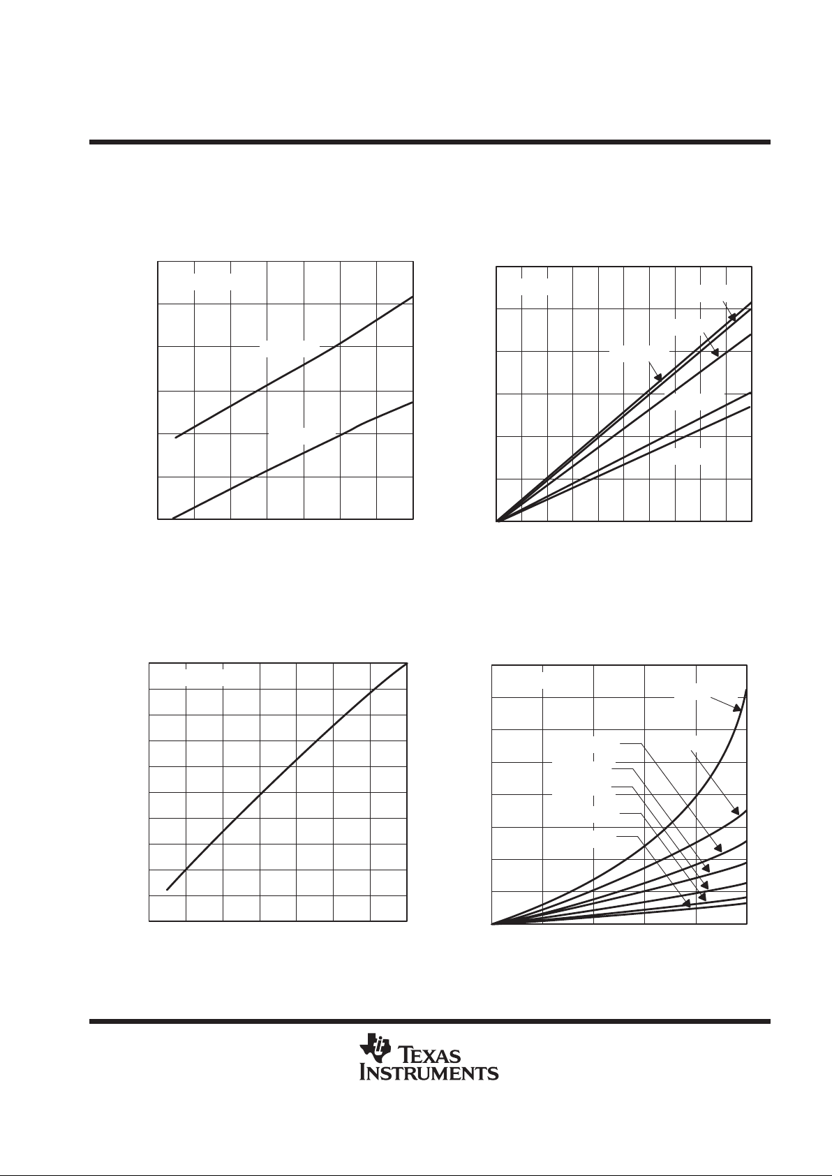
TYPICAL CHARACTERISTICS
Table of Graphs
vs Output current 7
IQQuiescent current
vs Input voltage 8
I
Q
Quiescent current TPS7348 vs Free-air temperature 9
vs Input voltage 10
IQQuiescent current
TPS7325
vs Free-air temperature 11
V
DO
Dropout voltage vs Output current 12
∆V
DO
Change in dropout voltage vs Free-air temperature 13
V
DO
Dropout voltage TPS7301 vs Output current 14
∆V
O
Change in output voltage vs Free-air temperature 15
V
O
Output voltage vs Input voltage 16
V
O
Output voltage TPS7325 vs Input voltage 17
Line regulation 18
TPS7301 vs Output current 19
TPS7325 vs Output current 20
p
TPS7330 vs Output current 21
VOOutput voltage
TPS7333 vs Output current 22
TPS7348 vs Output current 23
TPS7350 vs Output current 24
Output voltage response from enable (EN) 25
TPS7301 or TPS7333 26
TPS7325 27
p
TPS7348 or TPS7350 28
Load transient response
TPS7301 29
TPS7333 30
TPS7348 or TPS7350 31
Ripple rejection vs Frequency 32
Output spectral noise density vs Frequency 33
vs Output current 34
Compensation series resistance
C
o
= 4.7 µ
F
vs Added ceramic capacitance 35
(CSR)
vs Output current 36
C
o
= 10 µ
F
vs Added ceramic capacitance 37
r
DS(on)
Pass-element resistance vs Input voltage 38
V
I
Minimum input voltage for valid RESET vs Free-air temperature 39
V
IT–
Negative-going reset threshold vs Free-air temperature 40
I
OL(RESET)
RESET output current vs Input voltage 41
t
d
Reset time delay vs Free-air temperature 42
t
d
Distribution for reset delay 43
TPS7301Q, TPS7325Q, TPS7330Q, TPS7333Q, TPS7348Q, TPS7350Q
LOW-DROPOUT VOLTAGE REGULATORS
WITH INTEGRATED DELAYED RESET FUNCTION
SLVS124F – JUNE 1995 – REVISED JANUAR Y 1999
22
POST OFFICE BOX 655303 • DALLAS, TEXAS 75265
TYPICAL CHARACTERISTICS
Figure 7
QUIESCENT CURRENT
vs
OUTPUT CURRENT
– Quiescent Current –
Aµ
IO – Output Current – mA
I
Q
425
375
350
300
0 50 100 150 200 250
450
400
325
TA = 25°C
TPS73xx, VI = 10 V
TPS7350, VI = 6 V
TPS7333, VI = 4.3 V
TPS7348, VI = 5.85 V
275
TPS7330, VI = 4 V
TPS7325, VI = 3.5 V
Figure 8
QUIESCENT CURRENT
vs
INPUT VOLTAGE
VI – Input Voltage – V
– Quiescent Current –
Aµ
I
Q
200
150
50
0
0123456
250
350
500
78910
100
300
TPS7333
TPS7350
TA = 25°C
IO = 500 mA
TPS7301 With V
O
Programmed to 2.5 V
400
450
TPS7348
Figure 9
TPS7348
QUIESCENT CURRENT
vs
FREE-AIR TEMPERATURE
300
250
200
350
400
–50 – 25 0 25 50 75 100 125
VI = 5.85 V
IO = 500 mA
– Quiescent Current –
I
Q
Aµ
TA – Free-Air Temperature – °C
450
500
Figure 10
TPS7325
QUIESCENT CURRENT
vs
INPUT VOLTAGE
300
250
200
350
400
3 45678910
– Quiescent Current –
I
Q
Aµ
VI – Input Voltage – V
450
500
TA = 125°C
TA = 85°C
TA = 25°C
TA = 0°C
TA = –40°C
TPS7301Q, TPS7325Q, TPS7330Q, TPS7333Q, TPS7348Q, TPS7350Q
LOW-DROPOUT VOLTAGE REGULATORS
WITH INTEGRATED DELAYED RESET FUNCTION
SLVS124F – JUNE 1995 – REVISED JANUAR Y 1999
23
POST OFFICE BOX 655303 • DALLAS, TEXAS 75265
TYPICAL CHARACTERISTICS
Figure 11
TPS7325
QUIESCENT CURRENT
vs
FREE-AIR TEMPERATURE
300
250
200
350
400
–50 – 25 0 25 50 75 100 125
– Quiescent Current –
I
Q
Aµ
TA – Free-Air Temperature – °C
450
500
VI = 10 V
VI = 3.5 V
IL = 750 mA
Figure 12
DROPOUT VOLTAGE
vs
OUTPUT CURRENT
0.25
0.2
0.1
0.05
0
0.15
0 50 100 150 200 250 300
0.3
350 400 450 500
TA = 25°C
TPS7348
TPS7350
Dropout Voltage – V
IO – Output Current – mA
TPS7333
TPS7330
TPS7325
Figure 13
– Change In Dropout Voltage – mV
CHANGE IN DROPOUT VOLTAGE
vs
FREE-AIR TEMPERATURE
10
8
6
4
2
0
–2
–4
–6
–8
–10
–50 –25 0 25 50 75 100 125
IO = 100 mA
TA – Free-Air Temperature – °C
V
DO
∆
Figure 14
0 50 100 150 200 250
1.6
1.4
1.2
1
0.8
0.6
0.4
0.2
0
– Dropout Voltage – VV
DO
IO – Output Current – mA
TPS7301
DROPOUT VOLTAGE
vs
OUTPUT CURRENT
VI = 2.9 V
VI = 2.4 V
VI = 2.6 V
VI = 3.2 V
VI = 3.9 V
VI = 5.9 V
VI = 9.65 V
TA = 25°C
TPS7301Q, TPS7325Q, TPS7330Q, TPS7333Q, TPS7348Q, TPS7350Q
LOW-DROPOUT VOLTAGE REGULATORS
WITH INTEGRATED DELAYED RESET FUNCTION
SLVS124F – JUNE 1995 – REVISED JANUAR Y 1999
24
POST OFFICE BOX 655303 • DALLAS, TEXAS 75265
TYPICAL CHARACTERISTICS
Figure 15
CHANGE IN OUTPUT VOLTAGE
vs
FREE-AIR TEMPERATURE
0
– Change in Output Voltage – mV
10
15
20
5
–5
–10
–20
–50 – 25 0 25 50 75 100 125
V
O
–15
TA – Free-Air Temperature – °C
∆
VI = V
O(nom)
+ 1 V
IO = 100 mA
Figure 16
3
2
1
0
0123456
– Output Voltage – V
4
5
OUTPUT VOLTAGE
vs
INPUT VOLTAGE
6
78910
TPS7333
TA = 25°C
IO = 500 mA
TPS7350
TPS7348
V
O
VI – Input Voltage – V
TPS7301 With V
O
Programmed to 2.5 V
and TPS7325
Figure 17
1.5
1
0.5
0
0123456
– Output Voltage – V
2
2.5
TPS7325
OUTPUT VOLTAGE
vs
INPUT VOLTAGE
3
78910
TA = 25°C
100 mA
500 mA
V
O
VI – Input Voltage – V
Figure 18
0
4567
– Change In Output Voltage – mV
5
15
20
8910
10
–5
–10
–15
–20
TPS7350
TPS7348
TA = 25°C
IO = 250 mA
VI – Input Voltage – V
∆V
O
TPS7333
TPS7325
LINE REGULATION
TPS7301Q, TPS7325Q, TPS7330Q, TPS7333Q, TPS7348Q, TPS7350Q
LOW-DROPOUT VOLTAGE REGULATORS
WITH INTEGRATED DELAYED RESET FUNCTION
SLVS124F – JUNE 1995 – REVISED JANUAR Y 1999
25
POST OFFICE BOX 655303 • DALLAS, TEXAS 75265
TYPICAL CHARACTERISTICS
Figure 19
2.5
2.495
2.485
2.48
0 100 200 300
– Output Voltage – V
2.505
2.515
TPS7301
OUTPUT VOLTAGE
vs
OUTPUT CURRENT
2.52
400 500
2.49
2.51
V
O
IO – Output Current – mA
TA = 25°C
VO Programmed to 2.5 V
VI = 3.5 V
VI = 10 V
Figure 20
0 100 200 300 400 500
2.495
2.49
2.485
2.48
IO – Output Current – mA
2.515
2.51
2.505
2.5
2.52
VI = 10 V
VI = 3.5 V
– Output Voltage – V
TPS7325
OUTPUT VOLTAGE
vs
OUTPUT CURRENT
V
O
Figure 21
OUTPUT VOLTAGE
vs
OUTPUT CURRENT
TPS7330
3.06
3
2.94
2.85
0 100 300
– Output Voltage – V
3.12
500
3.15
3.09
3.03
2.97
2.91
2.88
200 400
V
O
IO – Output Current – mA
TA = 25°C
Figure 22
3.3
3.29
3.27
3.26
0 100 200 300
– Output Voltage – V
3.31
3.33
OUTPUT VOLTAGE
vs
OUTPUT CURRENT
3.34
400 500
3.28
3.32
TPS7333
TA = 25°C
VI = 10 V
VI = 4.3 V
V
O
IO – Output Current – mA

TPS7301Q, TPS7325Q, TPS7330Q, TPS7333Q, TPS7348Q, TPS7350Q
LOW-DROPOUT VOLTAGE REGULATORS
WITH INTEGRATED DELAYED RESET FUNCTION
SLVS124F – JUNE 1995 – REVISED JANUAR Y 1999
26
POST OFFICE BOX 655303 • DALLAS, TEXAS 75265
TYPICAL CHARACTERISTICS
Figure 23
OUTPUT VOLTAGE
vs
OUTPUT CURRENT
TPS7348
4.87
4.85
4.83
4.8
0 100 300
– Output Voltage – V
4.89
4.92
500
4.91
4.9
4.88
4.86
4.84
4.82
4.81
200 400
V
O
IO – Output Current – mA
TA = 25°C
VI = 5.85 V
VI = 10 V
Figure 24
OUTPUT VOLTAGE
vs
OUTPUT CURRENT
TPS7350
5.01
4.99
4.97
4.94
0 100 300
– Output Voltage – V
5.03
5.06
400 500
5.05
5.04
5.02
5
4.98
4.96
4.95
200
TA = 25°C
VI = 6 V
VI = 10 V
V
O
IO – Output Current – mA
– Output Voltage – V
OUTPUT VOLTAGE RESPONSE FROM
ENABLE (EN
)
0
2
4
6
0 20 40 60 80 100 120 140
EN Voltage – V
V
O
TA = 25°C
RL = 500 Ω
Co = 4.7 µF (CSR = 1Ω)
No Input Capacitance
V
O(nom)
Time – µs
–2
0
6
4
2
Figure 25

TPS7301Q, TPS7325Q, TPS7330Q, TPS7333Q, TPS7348Q, TPS7350Q
LOW-DROPOUT VOLTAGE REGULATORS
WITH INTEGRATED DELAYED RESET FUNCTION
SLVS124F – JUNE 1995 – REVISED JANUAR Y 1999
27
POST OFFICE BOX 655303 • DALLAS, TEXAS 75265
TYPICAL CHARACTERISTICS
LOAD TRANSIENT RESPONSE
200
100
0
–100
–200
– Output Current – mA
105
55
5
I
O
TPS7301 (WITH VO PROGRAMMED TO 2.5 V) OR TPS7333
t – Time – µs
0 100 200 300 400 500
TA = 25°C
VI = 6 V
CI = 0
Co = 4.7 µF (CSR = 1 Ω)
– Change in Output Voltage – mV∆V
O
–45
Figure 26
150
50
0
–50
–100
t – Time – µs
–200 –100 0 500100 600
– Change in Output Voltage – mV∆V
O
Figure 27
–150
–200
–250
–300 200 300 400
100
LOAD TRANSIENT RESPONSE
TPS7325
∆IO = 100 mA
VI = 6 V
CI = 0
Co = 10 µF
TA = 25°C

TPS7301Q, TPS7325Q, TPS7330Q, TPS7333Q, TPS7348Q, TPS7350Q
LOW-DROPOUT VOLTAGE REGULATORS
WITH INTEGRATED DELAYED RESET FUNCTION
SLVS124F – JUNE 1995 – REVISED JANUAR Y 1999
28
POST OFFICE BOX 655303 • DALLAS, TEXAS 75265
TYPICAL CHARACTERISTICS
LOAD TRANSIENT RESPONSE
200
100
0
–100
–200
105
55
5
TPS7348 OR TPS7350
t – Time – µs
0 100 200 300 400 500
VI = 6 V
CI = 0
Co = 4.7 µF
CSR = 1 Ω
TA = 25°C
– Change in Output Voltage – mV∆V
O
– Output Current – mA
I
O
–45
Figure 28
LINE TRANSIENT RESPONSE
100
50
0
–50
–100
6.5
6.25
6
TPS7301 WITH VO PROGRAMMED TO 2.5 V
t – Time – µs
0 100 200 300 400
TA = 25°C
CI = 0
Co = 4.7 µF (CSR = 1 Ω)
– Change in Output Voltage – mV∆V
O
– Input Voltage – V
V
I
5.75
Figure 29

TPS7301Q, TPS7325Q, TPS7330Q, TPS7333Q, TPS7348Q, TPS7350Q
LOW-DROPOUT VOLTAGE REGULATORS
WITH INTEGRATED DELAYED RESET FUNCTION
SLVS124F – JUNE 1995 – REVISED JANUAR Y 1999
29
POST OFFICE BOX 655303 • DALLAS, TEXAS 75265
TYPICAL CHARACTERISTICS
LINE TRANSIENT RESPONSE
200
100
0
–50
–100
– Input Voltage – V
6.5
6.25
6
V
I
TPS7333
t – Time – µs
5.75
0 100 200 300 400 500
TA = 25°C
CI = 0
Co = 4.7 µF (CSR = 1 Ω)
– Change in Output Voltage – mV∆V
O
Figure 30
LINE TRANSIENT RESPONSE
100
50
0
–50
–100
– Input Voltage – V
6.5
6.25
6
V
I
TPS7348 OR TPS7350
t – Time – µs
0 100 200 300 400 500
TA = 25°C
CI = 0
Co = 4.7 µF (CSR = 1 Ω)
– Change in Output Voltage – mV∆V
O
5.75
Figure 31

TPS7301Q, TPS7325Q, TPS7330Q, TPS7333Q, TPS7348Q, TPS7350Q
LOW-DROPOUT VOLTAGE REGULATORS
WITH INTEGRATED DELAYED RESET FUNCTION
SLVS124F – JUNE 1995 – REVISED JANUAR Y 1999
30
POST OFFICE BOX 655303 • DALLAS, TEXAS 75265
TYPICAL CHARACTERISTICS
Figure 32
30
10
0
Ripple Rejection – dB
40
50
f – Frequency – Hz
RIPPLE REJECTION
vs
FREQUENCY
60
20
10 100 1 K 10 K 100 K 1 M 10 M
TA = 25°C
No Input
Capacitance Added
VI = VO + 1 V
IO = 100 mA
Co = 4.7 µF (CSR = 1)
TPS7333
TPS7301 With
VO Programmed
to 2.5 V
TPS7348/
TPS7350
Figure 33
10 100 1 k 10 k 100 k
Co = 10 µF (CSR = 1 Ω)
Co = 4.7 µF (CSR = 1 Ω)
Co = 100 µF (CSR = 1 Ω)
f – Frequency – Hz
OUTPUT SPECTRAL-NOISE DENSITY
vs
FREQUENCY
10
1
0.1
0.01
TA = 25°C
No Input Capacitance Added
VI = VO + 1 V
Output Spectral-Noise Density –
V/
Hzµ
Figure 34
0.1
0.01
0 50 100 150 200 250
TYPICAL REGIONS OF STABILITY
COMPENSATION SERIES RESISTANCE (CSR)
†
vs
OUTPUT CURRENT
10
100
IO – Output Current – mA
CSR – Compensation Series Resistance – Ω
Region of Instability
1
TA = 25°C
VI = VO + 1 V
Co = 4.7 µF
No Added Ceramic Capacitance
No Input Capacitance Added
Region of Instability
Figure 35
0.1
0.01
0 0.1 0.2 0.3 0.4 0.5
TYPICAL REGIONS OF STABILITY
COMPENSATION SERIES RESISTANCE (CSR)
†
vs
ADDED CERAMIC CAPACITANCE
10
100
Added Ceramic Capacitance – µF
0.6 0.7 0.8 0.9 1
1
TA = 25°C
VI = VO + 1 V
IO = 500 mA
Co = 4.7 µF
No Input Capacitor Added
Region of Instability
Region of
Instability
CSR – Compensation Series Resistance – Ω

TPS7301Q, TPS7325Q, TPS7330Q, TPS7333Q, TPS7348Q, TPS7350Q
LOW-DROPOUT VOLTAGE REGULATORS
WITH INTEGRATED DELAYED RESET FUNCTION
SLVS124F – JUNE 1995 – REVISED JANUAR Y 1999
31
POST OFFICE BOX 655303 • DALLAS, TEXAS 75265
TYPICAL CHARACTERISTICS
Figure 36
0.1
0.01
0 50 100 150 200 250
TYPICAL REGIONS OF STABILITY
COMPENSATION SERIES RESISTANCE (CSR)
†
vs
OUTPUT CURRENT
10
100
IO – Output Current – mA
1
Region of Instability
TA = 25°C
VI = VO + 1 V
Co = 10 µF
No Added Ceramic Capacitance
No Input Capacitor Added
Region of Instability
CSR – Compensation Series Resistance – Ω
Figure 37
0.1
0.01
0 0.1 0.2 0.3 0.4 0.5
TYPICAL REGIONS OF STABILITY
COMPENSATION SERIES RESISTANCE (CSR)
†
vs
ADDED CERAMIC CAPACITANCE
10
100
Added Ceramic Capacitance – µF
1
0.6 0.7 0.8 0.9 1
Region of Instability
TA = 25°C
VI = VO + 1 V
IO = 500 mA
Co = 10 µF
No Input Capacitor Added
Region of
Instability
CSR – Compensation Series Resistance – Ω
Figure 38
0.4
0.3
0.2
0.1
2457
– Pass-Element Resistance –
0.5
PASS-ELEMENT RESISTANCE
vs
INPUT VOLTAGE
0.6
910
368
TA = 25°C
V
I(FB)
= 1.12 V
r
DS(on)
Ω
VI – Input Voltage – V
1
0.9
0.8
0.7
1.1
IO = 500 mA
IO = 100 mA
Figure 39
1.08
1.07
1.06
1.05
– Minimum Input Voltage For Valid RESET – V
1.09
MINIMUM INPUT VOLTAGE FOR VALID RESET
vs
FREE-AIR TEMPERATURE
1.1
–50 –25 0 25 50 75 100 125
V
I
TA – Free-Air Temperature – °C

TPS7301Q, TPS7325Q, TPS7330Q, TPS7333Q, TPS7348Q, TPS7350Q
LOW-DROPOUT VOLTAGE REGULATORS
WITH INTEGRATED DELAYED RESET FUNCTION
SLVS124F – JUNE 1995 – REVISED JANUAR Y 1999
32
POST OFFICE BOX 655303 • DALLAS, TEXAS 75265
TYPICAL CHARACTERISTICS
Figure 40
– Negative-Going Reset Threshold – mV
NEGATIVE-GOING RESET THRESHOLD
vs
FREE-AIR TEMPERATURE
15
10
5
0
–5
–10
–15
V
IT–
TA – Free-Air Temperature – °C
–50 –25 0 25 50 75 100 125
Figure 41
2
1.5
0.5
0
0123456
– RESET Output Current – mA
2.5
3.5
RESET OUTPUT CURRENT
vs
INPUT VOLTAGE
4
78910
1
3
I
OL
VI – Input Voltage – V
TPS7333
TPS7348
TPS7350
IL = 10 mA
VOL ≤ 0.4 V
TA = 25°C
Figure 42
192
191
196
190
– Reset Delay Time – ms
194
193
195
RESET DELAY TIME
vs
FREE-AIR TEMPERATURE
197
t
d
TA – Free-Air Temperature –°C
–50 –25 0 25 50 75 100 125
Figure 43
25
20
10
5
0
45
15
180 185 190 195
Percentage of Units – %
35
30
40
DISTRIBUTION FOR RESET DELAY
50
200 205 210
td – Reset Delay Time – ms
TA = 25°C
197 Devices

TPS7301Q, TPS7325Q, TPS7330Q, TPS7333Q, TPS7348Q, TPS7350Q
LOW-DROPOUT VOLTAGE REGULATORS
WITH INTEGRATED DELAYED RESET FUNCTION
SLVS124F – JUNE 1995 – REVISED JANUAR Y 1999
33
POST OFFICE BOX 655303 • DALLAS, TEXAS 75265
THERMAL INFORMATION
In response to system-miniaturization trends, integrated circuits are being offered in low-profile and fine-pitch
surface-mount packages. Implementation of many of today’s high-performance devices in these packages requires
special attention to power dissipation. Many system-dependent issues such as thermal coupling, airflow, added heat
sinks and convection surfaces, and the presence of other heat-generating components affect the power-dissipation
limits of a given component.
Three basic approaches for enhancing thermal performance are illustrated in this discussion:
D
Improving the power-dissipation capability of the PWB design
D
Improving the thermal coupling of the component to the PWB
D
Introducing airflow in the system
Figure 44 is an example of a thermally enhanced PWB layout for the 20-lead TSSOP package. This layout involves
adding copper on the PWB to conduct heat away from the device. The R
θJA
(thermal resistance, junction-to-ambient)
for this component/board system is illustrated in Figure 45. The family of curves illustrates the effect of increasing
the size of the copper-heat-sink surface area. The PWB is a standard FR4 board (L × W × H = 3.2 inch × 3.2 inch
× 0.062 inch); the board traces and heat sink area are 1-oz (per square foot) copper.
Figure 46 shows the thermal resistance for the same system with the addition of a thermally-conductive compound
between the body of the TSSOP package and the PWB copper routed directly beneath the device. The thermal
conductivity for the compound used in this analysis is 0.815 W/m × °C.
Using these figures to determine the system R
θJA
allows the maximum power-dissipation limit to be calculated with
the equation:
P
D(max)
+
T
J(max)
*
T
A
R
q
JA(system)
Where
T
J(max)
is the maximum allowable junction temperature; 150°C absolute maximum and 125°C
maximum recommended operating temperature for specified operation.
This limit should then be applied to the internal power dissipated by the TPS73xx regulator. The equation for
calculating total internal power dissipation of the TPS73xx is:
P
D(total)
+ǒVI*
V
O
Ǔ
IO)
VI
I
Q
Because the quiescent current of the TPS73xx family is very low, the second term is negligible, further simplifying
the equation to:
P
D(total)
+
ǒ
VI*
V
O
Ǔ
I
O
For a 20-lead TSSOP/FR4 board system with thermally conductive compound between the board and the device
body , where T
A
= 55°C, airflow = 100 ft/min, and copper heat sink area = 1 cm2, the maximum power-dissipation limit
can be calculated. As indicated in Figure 46, the system R
θJA
is 94°C/W; therefore, the maximum power-dissipation
limit is:
P
D(max)
+
T
J(max)
*
T
A
R
q
JA(system)
+
125 C*55 C
94 CńW
+
745 mW
°
°°
If the system implements a TPS7348 regulator where VI = 6 V and IO = 150 mA, the internal power dissipation is:
P
D(total)
+ǒVI*
V
O
Ǔ
IO+(6*
4.85) 0.150+173 mW

TPS7301Q, TPS7325Q, TPS7330Q, TPS7333Q, TPS7348Q, TPS7350Q
LOW-DROPOUT VOLTAGE REGULATORS
WITH INTEGRATED DELAYED RESET FUNCTION
SLVS124F – JUNE 1995 – REVISED JANUAR Y 1999
34
POST OFFICE BOX 655303 • DALLAS, TEXAS 75265
THERMAL INFORMATION
Comparing P
D(total)
with P
D(max)
reveals that the power dissipation in this example does not exceed the maximum
limit. When it does, one of two corrective actions can be taken. The power-dissipation limit can be raised by increasing
either the airflow or the heat-sink area. Alternatively , the internal power dissipation of the regulator can be lowered
by reducing either the input voltage or the load current. In either case, the above calculations should be repeated with
the new system parameters.
Copper Heat Sink
1 oz Cu
Figure 44. Thermally Enhanced PWB Layout (not to scale) for the 20-Pin TSSOP
Figure 45
110
90
70
50
0 50 100 150 200 250
130
150
THERMAL RESISTANCE, JUNCTION-TO-AMBIENT
vs
AIR FLOW
170
300
190
C/W
°
JAθ
R – Thermal Resistance, Junction-to-Ambient –
0 cm
2
8 cm
2
2 cm
2
4 cm
2
1 cm
2
Component/Board System
20-Lead TSSOP
Air Flow – ft/min
Figure 46
110
90
70
50
0 50 100 150 200 250
130
150
170
300
190
THERMAL RESISTANCE, JUNCTION-TO-AMBIENT
vs
AIR FLOW
0 cm
2
4 cm
2
2 cm
2
8 cm
2
1 cm
2
C/W
°
JAθ
R – Thermal Resistance, Junction-to-Ambient –
Component/Board System
20-Lead TSSOP
Includes Thermally Conductive
Compound Between Body and Board
Air Flow – ft/min

TPS7301Q, TPS7325Q, TPS7330Q, TPS7333Q, TPS7348Q, TPS7350Q
LOW-DROPOUT VOLTAGE REGULATORS
WITH INTEGRATED DELAYED RESET FUNCTION
SLVS124F – JUNE 1995 – REVISED JANUAR Y 1999
35
POST OFFICE BOX 655303 • DALLAS, TEXAS 75265
APPLICATION INFORMATION
The TPS73xx series of low-dropout (LDO) regulators overcome many of the shortcomings of earlier generation
LDOs, while adding features such as a power-saving shutdown mode and a supply-voltage supervisor. The
TPS73xx family includes five fixed-output voltage regulators: the TPS7325 (2.5 V), TPS7330 (3 V), TPS7333
(3.3 V), the TPS7348 (4.85 V), and the TPS7350 (5 V). The family also offers an adjustable device, the TPS7301
(adjustable from 1.2 V to 9.75 V).
device operation
The TPS73xx, unlike many other LDOs, features very low quiescent currents that remain virtually constant even
with varying loads. Conventional LDO regulators use a pnp-pass element, the base current of which is directly
proportional to the load current through the regulator (I
B
= IC/β). Close examination of the data sheets reveals
that such devices are typically specified under near no-load conditions; actual operating currents are much
higher as evidenced by typical quiescent current versus load current curves (see Figure 7). The TPS73xx uses
a PMOS transistor to pass current; because the gate of the PMOS element is voltage driven, operating currents
are low and invariable over the full load range. The TPS73xx specifications reflect actual performance under
load.
Another pitfall associated with the pnp-pass element is its tendency to saturate when the device goes into
dropout. The resulting drop in β forces an increase in IB to maintain the load. During power-up, this translates
to large start-up currents. Systems with limited supply current may fail to start up. In battery-powered systems,
it means rapid battery discharge when the voltage decays below the minimum required for regulation. The
TPS73xx quiescent current remains low even when the regulator drops out, thus eliminating both problems.
Included in the TPS73xx family is a 4.85-V regulator, the TPS7348. Designed specifically for 5-V cellular
systems, its 4.85-V output, regulated to within ± 2%, allows for operation within the low-end limit of 5-V systems
specified to ± 5% tolerance; therefore, maximum regulated operating lifetime is obtained from a battery pack
before the device drops out, adding crucial talk minutes between charges.
The TPS73xx family also features a shutdown mode that places the output in the high-impedance state
(essentially equal to the feedback-divider resistance) and reduces quiescent current to under 0.5 µA. When the
shutdown feature is not used, EN
should be tied to ground. Response to an enable transition is quick; regulated
output voltage is reestablished in typically 120 µs.
minimum load requirements
The TPS73xx family is stable even at zero load; no minimum load is required for operation.
SENSE connection
The SENSE terminal of fixed-output devices must be connected to the regulator output for proper functioning
of the regulator. Normally , this connection should be as short as possible; however , the connection can be made
near a critical circuit (remote sense) to improve performance at that point. Internally, SENSE connects to a
high-impedance wide-bandwidth amplifier through a resistor-divider network, and noise pickup feeds through
to the regulator output. It is essential to route the SENSE connection in such a way as to minimize/avoid noise
pickup. Adding an RC network between SENSE and OUT to filter noise is not recommended because it can
cause the regulator to oscillate.
external capacitor requirements
An input capacitor is not required; however, a ceramic bypass capacitor (0.047 pF to 0.1 µF) improves load
transient response and noise rejection when the TPS73xx is located more than a few inches from the power
supply. A higher-capacitance electrolytic capacitor may be necessary if large (hundreds of milliamps) load
transients with fast rise times are anticipated.

TPS7301Q, TPS7325Q, TPS7330Q, TPS7333Q, TPS7348Q, TPS7350Q
LOW-DROPOUT VOLTAGE REGULATORS
WITH INTEGRATED DELAYED RESET FUNCTION
SLVS124F – JUNE 1995 – REVISED JANUAR Y 1999
36
POST OFFICE BOX 655303 • DALLAS, TEXAS 75265
APPLICATION INFORMATION
external capacitor requirements (continued)
As with most LDO regulators, the TPS73xx family requires an output capacitor for stability. A low-ESR 10-µF
solid-tantalum capacitor connected from the regulator output to ground is sufficient to ensure stability over the
full load range (see Figure 42). Adding high-frequency ceramic or film capacitors (such as power-supply bypass
capacitors for digital or analog ICs) can cause the regulator to become unstable unless the ESR of the tantalum
capacitor is less than 1.2 Ω over temperature. Capacitors with published ESR specifications such as the
AVX TPSD106M035R0300 and the Sprague 593D106X0035D2W work well because the maximum ESR at
25°C is 300 mΩ (typically, the ESR in solid-tantalum capacitors increases by a factor of 2 or less when the
temperature drops from 25°C to –40°C). Where component height and/or mounting area is a problem,
physically smaller, 10-µF devices can be screened for ESR. Figures 29 through 32 show the stable regions of
operation using different values of output capacitance with various values of ceramic load capacitance.
In applications with little or no high-frequency bypass capacitance (< 0.2 µF), the output capacitance can be
reduced to 4.7 µF, provided ESR is maintained between 0.7 and 2.5 Ω. Because capacitor minimum ESR is
seldom if ever specified, it may be necessary to add a 0.5-Ω to 1-Ω resistor in series with the capacitor and limit
ESR to 1.5 Ω maximum. As shown in the CSR graphs (Figures 29 through 32), minimum ESR is not a problem
when using 10-µF or larger output capacitors.
Below is a partial listing of surface-mount capacitors usable with the TPS73xx family. This information, along
with the CSR graphs, is included to assist in selection of suitable capacitance for the user’s application. When
necessary to achieve low height requirements along with high output current and/or high ceramic load
capacitance, several higher ESR capacitors can be used in parallel to meet the guidelines above.
All load and temperature conditions with up to 1 µF of added ceramic load capacitance:
PART NO. MFR. VALUE MAX ESR
†
SIZE (H × L × W)
†
T421C226M010AS Kemet 22 µF, 10 V 0.5 2.8 × 6 × 3.2
593D156X0025D2W Sprague 15 µF, 25 V 0.3 2.8 × 7.3 × 4.3
593D106X0035D2W Sprague 10 µF, 35 V 0.3 2.8 × 7.3 × 4.3
TPSD106M035R0300 AVX 10 µF, 35 V 0.3 2.8 × 7.3 × 4.3
Load < 200 mA, ceramic load capacitance < 0.2 µF, full temperature range:
PART NO. MFR. VALUE MAX ESR
†
SIZE (H × L × W)
†
592D156X0020R2T Sprague 15 µF, 20 V 1.1 1.2 × 7.2 × 6
595D156X0025C2T Sprague 15 µF, 25 V 1 2.5 × 7.1 × 3.2
595D106X0025C2T Sprague 10 µF, 25 V 1.2 2.5 × 7.1 × 3.2
293D226X0016D2W Sprague 22 µF, 16 V 1.1 2.8 × 7.3 × 4.3
Load < 100 mA, ceramic load capacitance < 0.2 µF, full temperature range:
PART NO. MFR. VALUE MAX ESR
†
SIZE (H × L × W)
†
195D106X06R3V2T Sprague 10 µF, 6.3 V 1.5 1.3 × 3.5 × 2.7
195D106X0016X2T Sprague 10 µF, 16 V 1.5 1.3 × 7 × 2.7
595D156X0016B2T Sprague 15 µF, 16 V 1.8 1.6 × 3.8 × 2.6
695D226X0015F2T Sprague 22 µF, 15 V 1.4 1.8 × 6.5 × 3.4
695D156X0020F2T Sprague 15 µF, 20 V 1.5 1.8 × 6.5 × 3.4
695D106X0035G2T Sprague 10 µF, 35 V 1.3 2.5 × 7.6 × 2.5
†
Size is in mm. ESR is maximum resistance at 100 kHz and TA = 25°C. Listings are sorted by height.
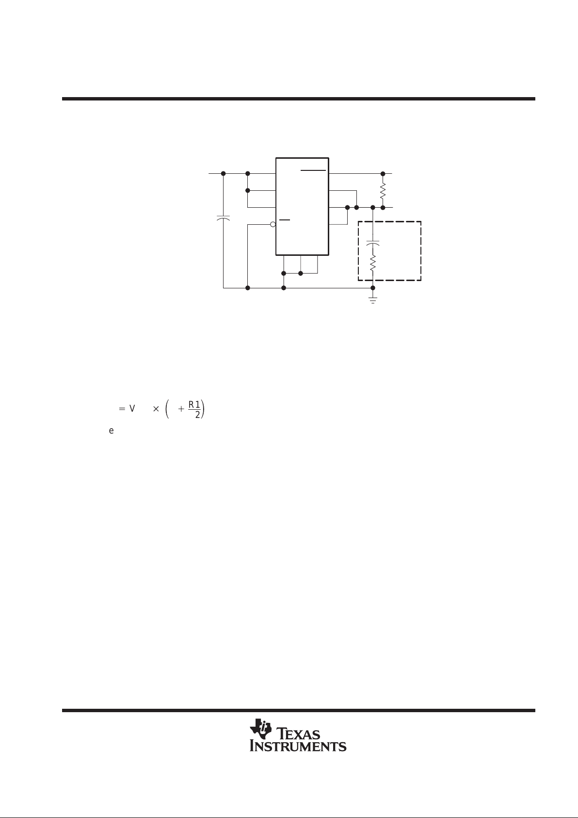
TPS7301Q, TPS7325Q, TPS7330Q, TPS7333Q, TPS7348Q, TPS7350Q
LOW-DROPOUT VOLTAGE REGULATORS
WITH INTEGRATED DELAYED RESET FUNCTION
SLVS124F – JUNE 1995 – REVISED JANUAR Y 1999
37
POST OFFICE BOX 655303 • DALLAS, TEXAS 75265
APPLICATION INFORMATION
external capacitor requirements (continued)
†
TPS7333, TPS7348, TPS7350 (fixed-voltage options)
SENSE
RESET
OUT
OUT
9
8
6
10
IN
IN
IN
EN
GND
321
20
15
14
13
V
I
0.1 µF
To System
Reset
CSR = 1 Ω
V
O
10 µF
+
TPS73xxPW
†
250 kΩ
Figure 47. Typical Application Circuit
programming the TPS7301 adjustable LDO regulator
Programming the adjustable regulators is accomplished using an external resistor divider as shown in
Figure 43. The equation governing the output voltage is:
VO+
V
ref
ǒ1
)
R1
R2
Ǔ
Where
V
ref
= reference voltage, 1.182 V typ
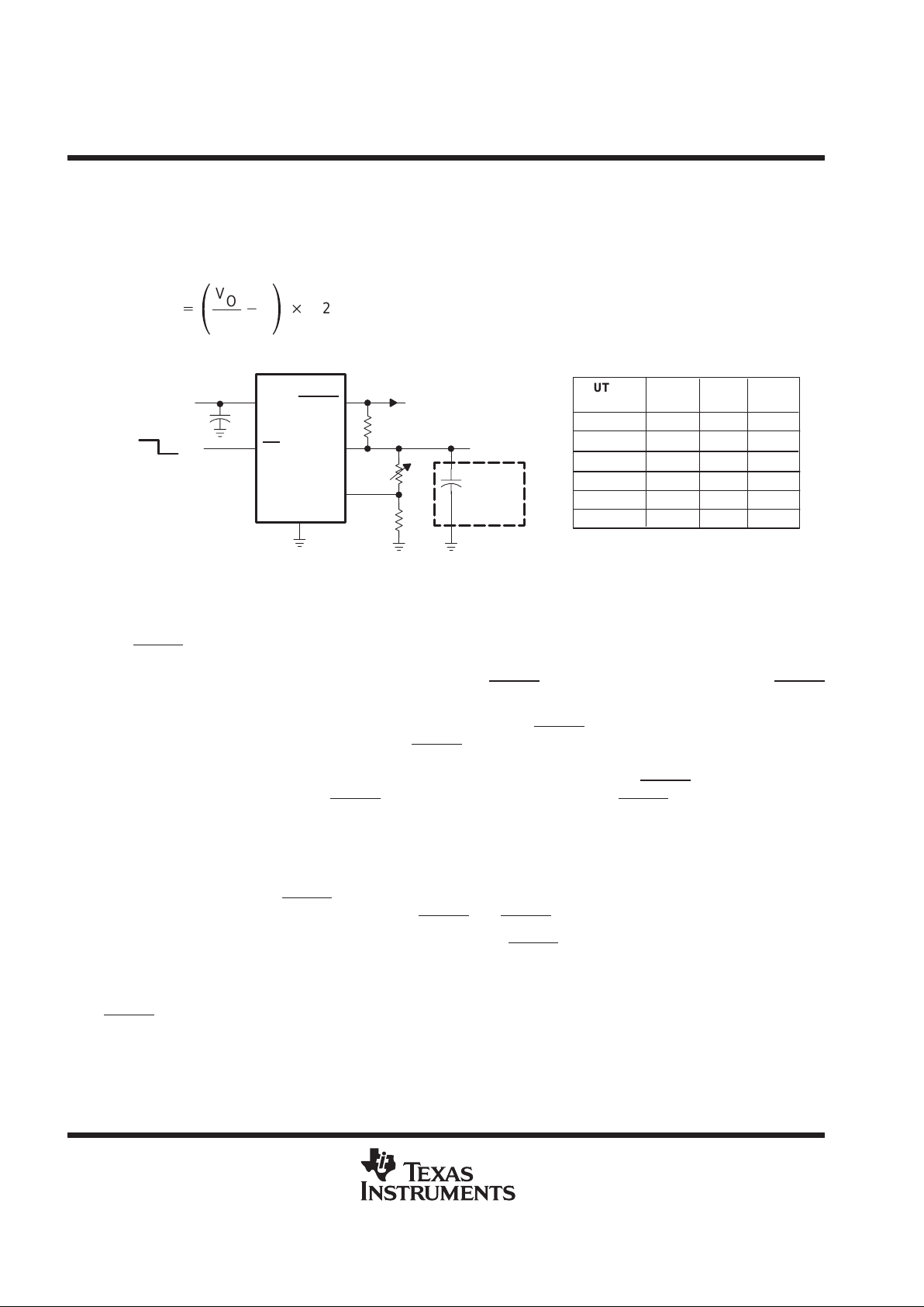
TPS7301Q, TPS7325Q, TPS7330Q, TPS7333Q, TPS7348Q, TPS7350Q
LOW-DROPOUT VOLTAGE REGULATORS
WITH INTEGRATED DELAYED RESET FUNCTION
SLVS124F – JUNE 1995 – REVISED JANUAR Y 1999
38
POST OFFICE BOX 655303 • DALLAS, TEXAS 75265
APPLICATION INFORMATION
Resistors R1 and R2 should be chosen for approximately 7-µA divider current. A recommended value for R2
is 169 kΩ with R1 adjusted for the desired output voltage. Smaller resistors can be used, but offer no inherent
advantage and consume more power. Larger values of R1 and R2 should be avoided as leakage currents at
FB will introduce an error. Solving for R1 yields a more useful equation for choosing the appropriate resistance:
R1
+
ǒ
V
O
V
ref
*
1
Ǔ
R2
OUTPUT
VOLTAGE
R1 R2
2.5 V
3.3 V
3.6 V
4 V
5 V
6.4 V
UNIT
191
309
348
402
549
750
169
169
169
169
169
169
kΩ
kΩ
kΩ
kΩ
kΩ
kΩ
OUTPUT VOLTAGE
PROGRAMMING GUIDE
V
O
RESET
OUT
FB
R1
R2
GND
EN
IN
<0.5 V
>2.7 V
TPS7301
To System
Reset
0.1 µF
250 kΩ
+
V
I
CSR = 1 Ω
10 µF
Figure 48. TPS7301 Adjustable LDO Regulator Programming
undervoltage supervisor function
The RESET output of the TPS73xx initiates a reset in microcomputer and microprocessor systems in the event
of an undervoltage condition. An internal comparator in the TPS73xx monitors the output voltage of the regulator
to detect the undervoltage condition. When that occurs, the RESET
output transistor turns on taking the RESET
signal low.
On power up, the output voltage tracks the input voltage. The RESET
output becomes active (low) as V
I
approaches the minimum required for a valid RESET signal (specified at 1.5 V for 25°C and 1.9 V over full
recommended operating temperature range). When the output voltage reaches the appropriate positive-going
input threshold (V
IT+
), a 200-ms (typical) timeout period begins during which the RESET output remains low.
Once the timeout has expired, the RESET output becomes inactive. Since the RESET output is an open-drain
NMOS, a pullup resistor should be used to ensure that a logic-high signal is indicated.
The supply-voltage-supervisor function is also activated during power-down. As the input voltage decays and
after the dropout voltage is reached, the output voltage tracks linearly with the decaying input voltage. When
the output voltage drops below the specified negative-going input threshold (V
IT–
— see electrical
characteristics tables), the RESET output becomes active (low). It is important to note that if the input voltage
decays below the minimum required for a valid RESET, the RESET is undefined.
Since the circuit is monitoring the regulator output voltage, the RESET output can also be triggered by disabling
the regulator or by any fault condition that causes the output to drop below V
IT–
. Examples of fault conditions
include a short circuit on the output and a low input voltage. Once the output voltage is reestablished, either by
reenabling the regulator or removing the fault condition, then the internal timer is initiated, which holds the
RESET
signal active during the 200-ms (typical) timeout period.

TPS7301Q, TPS7325Q, TPS7330Q, TPS7333Q, TPS7348Q, TPS7350Q
LOW-DROPOUT VOLTAGE REGULATORS
WITH INTEGRATED DELAYED RESET FUNCTION
SLVS124F – JUNE 1995 – REVISED JANUAR Y 1999
39
POST OFFICE BOX 655303 • DALLAS, TEXAS 75265
APPLICATION INFORMATION
undervoltage supervisor function (continued)
Transient loads or line pulses can also cause a reset to occur if proper care is not taken in selecting the input
and output capacitors. Load transients that are faster than 5 µs can cause a reset if high-ESR output capacitors
(greater than approximately 7 Ω) are used. A 1-µs transient causes a reset when using an output capacitor with
greater than 3.5 Ω of ESR. Note that the output-voltage spike during the transient can drop well below the reset
threshold and still not trip if the transient duration is short. A 1-µs transient must drop at least 500 mV below the
threshold before tripping the reset circuit. A 2-µs transient trips RESET
at just 400 mV below the threshold.
Lower-ESR output capacitors help by reducing the drop in output voltage during a transient and should be used
when fast transients are expected.
NOTE:
V
IT+
= V
IT–
+Hysteresis
output noise
The TPS73xx has very low output noise, with a spectral noise density < 2 µV/√Hz. This is important when
noise-susceptible systems, such as audio amplifiers, are powered by the regulator.
regulator protection
The TPS73xx PMOS-pass transistor has a built-in back diode that safely conducts reverse currents when the
input voltage drops below the output voltage (e.g., during power down). Current is conducted from the output
to the input and is not internally limited. If extended reverse voltage is anticipated, external limiting might be
appropriate.
The TPS73xx also features internal current limiting and thermal protection. During normal operation, the
TPS73xx limits output current to approximately 1 A. When current limiting engages, the output voltage scales
back linearly until the overcurrent condition ends. While current limiting is designed to prevent gross device
failure, care should be taken not to exceed the power dissipation ratings of the package. If the temperature of
the device exceeds 165°C, thermal-protection circuitry shuts it down. Once the device has cooled, regulator
operation resumes.

TPS7301Q, TPS7325Q, TPS7330Q, TPS7333Q, TPS7348Q, TPS7350Q
LOW-DROPOUT VOLTAGE REGULATORS
WITH INTEGRATED DELAYED RESET FUNCTION
SLVS124F – JUNE 1995 – REVISED JANUAR Y 1999
40
POST OFFICE BOX 655303 • DALLAS, TEXAS 75265
MECHANICAL DATA
D (R-PDSO-G**) PLASTIC SMALL-OUTLINE PACKAGE
14 PIN SHOWN
4040047/D 10/96
0.228 (5,80)
0.244 (6,20)
0.069 (1,75) MAX
0.010 (0,25)
0.004 (0,10)
1
14
0.014 (0,35)
0.020 (0,51)
A
0.157 (4,00)
0.150 (3,81)
7
8
0.044 (1,12)
0.016 (0,40)
Seating Plane
0.010 (0,25)
PINS **
0.008 (0,20) NOM
A MIN
A MAX
DIM
Gage Plane
0.189
(4,80)
(5,00)
0.197
8
(8,55)
(8,75)
0.337
14
0.344
(9,80)
16
0.394
(10,00)
0.386
0.004 (0,10)
M
0.010 (0,25)
0.050 (1,27)
0°–8°
NOTES: A. All linear dimensions are in inches (millimeters).
B. This drawing is subject to change without notice.
C. Body dimensions do not include mold flash or protrusion, not to exceed 0.006 (0,15).
D. Falls within JEDEC MS-012

TPS7301Q, TPS7325Q, TPS7330Q, TPS7333Q, TPS7348Q, TPS7350Q
LOW-DROPOUT VOLTAGE REGULATORS
WITH INTEGRATED DELAYED RESET FUNCTION
SLVS124F – JUNE 1995 – REVISED JANUAR Y 1999
41
POST OFFICE BOX 655303 • DALLAS, TEXAS 75265
MECHANICAL DATA
P (R-PDIP-T8) PLASTIC DUAL-IN-LINE PACKAGE
4040082/B 03/95
0.310 (7,87)
0.290 (7,37)
0.010 (0,25) NOM
0.400 (10,60)
0.355 (9,02)
58
41
0.020 (0,51) MIN
0.070 (1,78) MAX
0.240 (6,10)
0.260 (6,60)
0.200 (5,08) MAX
0.125 (3,18) MIN
0.015 (0,38)
0.021 (0,53)
Seating Plane
M
0.010 (0,25)
0.100 (2,54)
0°–15°
NOTES: A. All linear dimensions are in inches (millimeters).
B. This drawing is subject to change without notice.
C. Falls within JEDEC MS-001

TPS7301Q, TPS7325Q, TPS7330Q, TPS7333Q, TPS7348Q, TPS7350Q
LOW-DROPOUT VOLTAGE REGULATORS
WITH INTEGRATED DELAYED RESET FUNCTION
SLVS124F – JUNE 1995 – REVISED JANUAR Y 1999
42
POST OFFICE BOX 655303 • DALLAS, TEXAS 75265
MECHANICAL DATA
PW (R-PDSO-G**) PLASTIC SMALL-OUTLINE PACKAGE
4040064/E 08/96
14 PIN SHOWN
Seating Plane
1,20 MAX
1
A
7
14
0,19
4,50
4,30
8
6,20
6,60
0,30
0,75
0,50
0,25
Gage Plane
0,15 NOM
0,65
M
0,10
0°–8°
0,10
PINS **
A MIN
A MAX
DIM
2,90
3,10
8
4,90
5,10
14
6,60
6,404,90
5,10
16
7,70
20
7,90
24
9,60
9,80
28
0,15
0,05
NOTES: A. All linear dimensions are in millimeters.
B. This drawing is subject to change without notice.
C. Body dimensions do not include mold flash or protrusion not to exceed 0,15.
D. Falls within JEDEC MO-153

IMPORTANT NOTICE
T exas Instruments and its subsidiaries (TI) reserve the right to make changes to their products or to discontinue
any product or service without notice, and advise customers to obtain the latest version of relevant information
to verify, before placing orders, that information being relied on is current and complete. All products are sold
subject to the terms and conditions of sale supplied at the time of order acknowledgement, including those
pertaining to warranty, patent infringement, and limitation of liability.
TI warrants performance of its semiconductor products to the specifications applicable at the time of sale in
accordance with TI’s standard warranty. Testing and other quality control techniques are utilized to the extent
TI deems necessary to support this warranty. Specific testing of all parameters of each device is not necessarily
performed, except those mandated by government requirements.
CERT AIN APPLICATIONS USING SEMICONDUCTOR PRODUCTS MAY INVOLVE POTENTIAL RISKS OF
DEATH, PERSONAL INJURY, OR SEVERE PROPERTY OR ENVIRONMENTAL DAMAGE (“CRITICAL
APPLICATIONS”). TI SEMICONDUCTOR PRODUCTS ARE NOT DESIGNED, AUTHORIZED, OR
WARRANTED TO BE SUITABLE FOR USE IN LIFE-SUPPORT DEVICES OR SYSTEMS OR OTHER
CRITICAL APPLICATIONS. INCLUSION OF TI PRODUCTS IN SUCH APPLICA TIONS IS UNDERSTOOD T O
BE FULLY AT THE CUSTOMER’S RISK.
In order to minimize risks associated with the customer’s applications, adequate design and operating
safeguards must be provided by the customer to minimize inherent or procedural hazards.
TI assumes no liability for applications assistance or customer product design. TI does not warrant or represent
that any license, either express or implied, is granted under any patent right, copyright, mask work right, or other
intellectual property right of TI covering or relating to any combination, machine, or process in which such
semiconductor products or services might be or are used. TI’s publication of information regarding any third
party’s products or services does not constitute TI’s approval, warranty or endorsement thereof.
Copyright 1999, Texas Instruments Incorporated
 Loading...