

Datasheet TPS71H50QPWPR, TPS71H50QPWPLE, TPS71H48QPWPR, TPS71H48QPWPLE, TPS71H33QPWPR Datasheet (Texas Instruments)
...
TPS71H01Q, TPS71H33Q, TPS71H48Q, TPS71H50Q
LOW-DROPOUT VOLTAGE REGULATORS
SLVS152A – NOVEMBER 1996 – REVISED JANUAR Y 1997
D
Available in 5-V, 4.85-V, and 3.3-V
Fixed-Output and Adjustable Versions
D
Very Low-Dropout Voltage . . . Maximum of
32 mV at I
D
Very Low Quiescent Current – Independent
= 100 mA (TPS71H50)
O
of Load...285 µA Typ
D
Extremely Low Sleep-State Current
0.5 µA Max
D
2% Tolerance Over Specified Conditions
For Fixed-Output Versions
D
Output Current Range of 0 mA to 500 mA
D
TSSOP Package Option Offers Reduced
Component Height for Space-Critical
Applications
D
Thermally Enhanced Surface-Mount
GND/HEATSINK
GND/HEATSINK
GND
NC
EN
IN
IN
NC
GND/HEATSINK
GND/HEATSINK
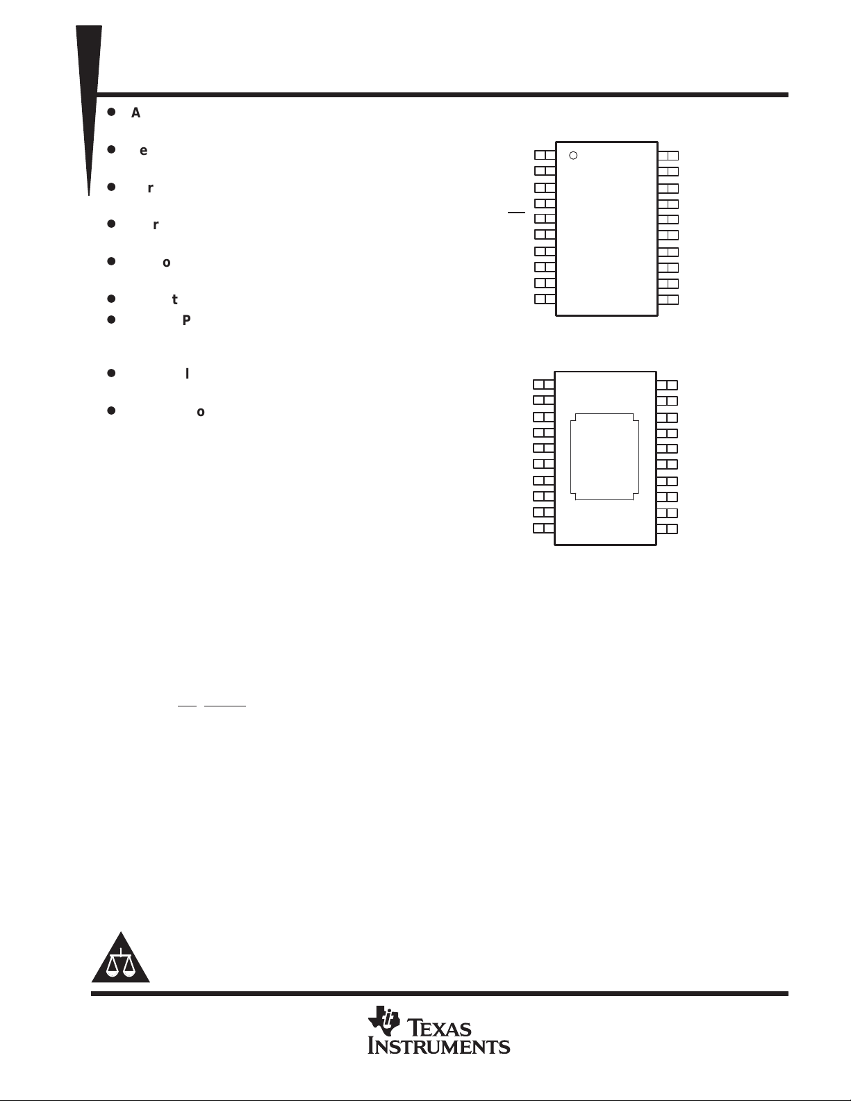
PWP PACKAGE
(TOP VIEW)
1
2
3
4
5
6
7
8
9
10
PWP PACKAGE
(BOTTOM VIEW)
20
19
18
17
16
15
14
13
12
11
GND/HEATSINK
GND/HEATSINK
NC
NC
PG
SENSE†/FB
OUT
OUT
GND/HEATSINK
GND/HEATSINK
Package
D
Power-Good (PG) Status Output
description
The TPS71Hxx integrated circuits are a family of
Thermal
Pad
micropower low-dropout (LDO) voltage regulators. An order of magnitude reduction in dropout
voltage and quiescent current over conventional
LDO performance is achieved by replacing the
typical pnp pass transistor with a PMOS device.
Because the PMOS device behaves as a
low-value resistor, the dropout voltage is very low
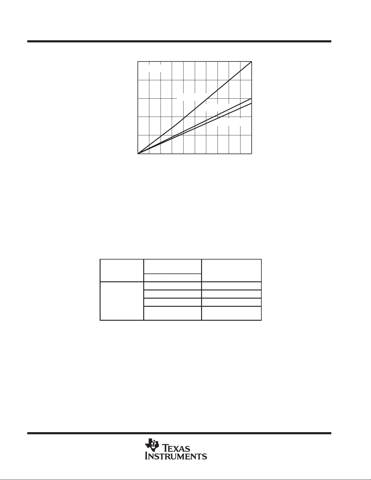
(maximum of 32 mV at an output current of
NC – No internal connection
†
SENSE – Fixed voltage options only (TPS71H33,
TPS71H48, and TPS71H50)
‡
FB – Adjustable version only (TPS71H01)
100 mA for the TPS71H50) and is directly
proportional to the output current (see Figure 1). Additionally, since the PMOS pass element is a voltage-driven
device, the quiescent current is very low and remains independent of output loading (typically 285 µA over the
full range of output current, 0 mA to 500 mA). These two key specifications yield a significant improvement in
operating life for battery-powered systems. The LDO family also features a sleep mode; applying a TTL high
signal to EN
(enable) shuts down the regulator, reducing the quiescent current to 0.5 µA maximum at TJ = 25°C.
‡
Please be aware that an important notice concerning availability, standard warranty, and use in critical applications of
Texas Instruments semiconductor products and disclaimers thereto appears at the end of this data sheet.
PRODUCTION DATA information is current as of publication date.
Products conform to specifications per the terms of Texas Instruments
standard warranty. Production processing does not necessarily include
testing of all parameters.
POST OFFICE BOX 655303 • DALLAS, TEXAS 75265
Copyright 1997, Texas Instruments Incorporated
1
TPS71H01Q, TPS71H33Q, TPS71H48Q, TPS71H50Q
J
(PWP)
LOW-DROPOUT VOLTAGE REGULATORS
SLVS152A – NOVEMBER 1996 – REVISED JANUAR Y 1997
description (continued)
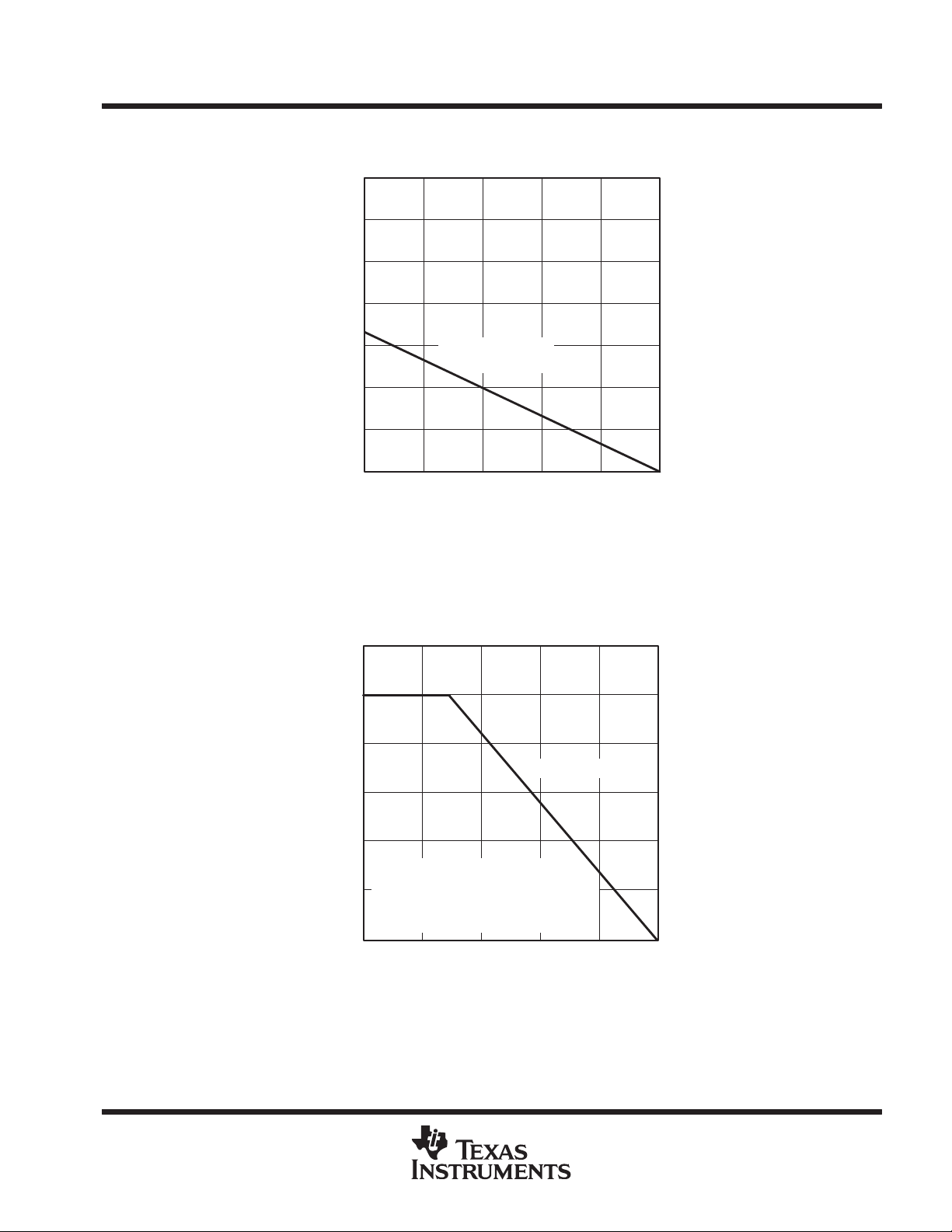
0.25
TA = 25°C
0.2
0.15
0.1
Dropout Voltage – V
0.05
0
0 0.05 0.1 0.15 0.2 0.25 0.3
TPS71H33
TPS71H48
TPS71H50
0.35 0.4 0.45 0.5
IO – Output Current – A
Figure 1. Dropout Voltage Versus Output Current
Power good (PG) reports low output voltage and can be used to implement a power-on reset or a low-battery
indicator.
The TPS71Hxx is offered in 3.3-V, 4.85-V, and 5-V fixed-voltage versions and in an adjustable version
(programmable over the range of 1.2 V to 9.75 V). Output voltage tolerance is specified as a maximum of 2%
over line, load, and temperature ranges (3% for adjustable version). The TPS71Hxx family is available in a
TSSOP (20-pin) thermally enhanced surface-mount power package. The package has an innovative thermal
pad that, when soldered to the printed-wiring board (PWB), enables the device to dissipate several watts of
power (see Thermal Information section). Maximum height of the package is 1.2 mm.
AVAILABLE OPTIONS
OUTPUT VOLTAGE
T
–55°C to 150°C
†
The PWP package is only available left-end taped and reeled, as indicated
by the LE suffix on the device type. The TPS71H01Q is programmable using
an external resistor divider (see application information).
(V)
MIN TYP MAX
4.9 5 5.1 TPS71H50QPWPLE
4.75 4.85 4.95 TPS71H48QPWPLE
3.23 3.3 3.37 TPS71H33QPWPLE
Adjustable
1.2 V to 9.75 V
†
TSSOP
TPS71H01QPWPLE
2
POST OFFICE BOX 655303 • DALLAS, TEXAS 75265
TPS71H01Q, TPS71H33Q, TPS71H48Q, TPS71H50Q
LOW-DROPOUT VOLTAGE REGULATORS
SLVS152A – NOVEMBER 1996 – REVISED JANUAR Y 1997
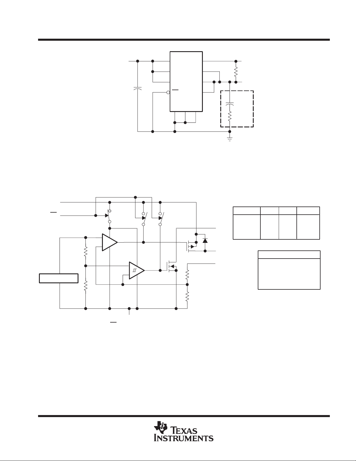
TPS71Hxx
†
functional block diagram
IN
EN
V
ref
= 1.178 V
†
_
+
10
8
IN
9
IN
SENSE
IN
6
EN
GND
V
I
0.1 µF
†
TPS71H33, TPS71H48, TPS71H50 (fixed-voltage options)
‡
Capacitor selection is nontrivial. See application information section
for details.
PG
OUT
OUT
20
15
14
13
+
10 µF
321
CSR
Figure 2. Typical Application Configuration
DEVICE
TPS71H01
TPS71H33
TPS71H48
TPS71H50
NOTE A: Resistors are nominal values only.
1.12 V
††
+
_
PG
OUT
SENSE‡/FB
R1
PG
V
O
‡
C
O
RESISTOR DIVIDER OPTIONS
∞
0
420
726
756
COMPONENT COUNT
MOS transistors
Bilpolar transistors
Diodes
Capacitors
Resistors
233
233
233
UNITR1 R2
Ω
kΩ
kΩ
kΩ
464
41
4
17
76
R2
†
Switch positions are shown with EN
‡
For most applications, SENSE should be externally connected to OUT as close as possible to the device. (For other implementations, refer
to SENSE-pin connection discussion in Applications Information section.)
GND
low (active).
POST OFFICE BOX 655303 • DALLAS, TEXAS 75265
3
TPS71H01Q, TPS71H33Q, TPS71H48Q, TPS71H50Q
PACKAGE
A
PACKAGE
C
LOW-DROPOUT VOLTAGE REGULATORS
SLVS152A – NOVEMBER 1996 – REVISED JANUAR Y 1997
absolute maximum ratings over operating free-air temperature range (unless otherwise noted)
‡
Input voltage range
Output current, I
Continuous total power dissipation See Dissipation Rating Tables 1 and 2. . . . . . . . . . . . . . . . . . . . . . . . . . . . .
Operating virtual junction temperature range, T
Storage temperature range, T
Lead temperature 1,6 mm (1/16 inch) from case for 10 seconds 260°C. . . . . . . . . . . . . . . . . . . . . . . . . . . . . . .
†
Stresses beyond those listed under “absolute maximum ratings” may cause permanent damage to the device. These are stress ratings only, and
functional operation of the device at these or any other conditions beyond those indicated under “recommended operating conditions” is not
implied. Exposure to absolute-maximum-rated conditions for extended periods may affect device reliability.
‡
All voltage values are with respect to network terminal ground.
§
Dissipation rating tables and figures are provided for maintenance of junction temperature at or below
absolute maximum temperature of 150°C. For guidelines on maintaining junction temperature within
recommended operating range, see the Thermal Information section.
¶
Refer to Thermal Information section for detailed power dissipation considerations when using the
TSSOP packages.
, VI, PG, SENSE, EN –0.3 V to 11 V. . . . . . . . . . . . . . . . . . . . . . . . . . . . . . . . . . . . . . . . . . . .
2 A. . . . . . . . . . . . . . . . . . . . . . . . . . . . . . . . . . . . . . . . . . . . . . . . . . . . . . . . . . . . . . . . . . . . . . . . . . .
O
–55°C to 150°C. . . . . . . . . . . . . . . . . . . . . . . . . . . . . . . . . . . . .
–65°C to 150°C. . . . . . . . . . . . . . . . . . . . . . . . . . . . . . . . . . . . . . . . . . . . . . . . . . .
stg
DISSIPATION RA TING TABLE 1 – FREE-AIR TEMPERATURE (see Figure 3)
T
≤ 25°C DERATING FACTOR T
POWER RATING ABOVE TA = 25°CAPOWER RATINGAPOWER RATING
¶
PWP
DISSIPATION RA TING TABLE 2 – CASE TEMPERATURE (see Figure 4)
¶
PWP
700 mW 5.6 mW/°C 448 mW 140 mW
T
≤ 62.5°C DERATING FACTOR T
POWER RATING ABOVE TC = 62.5°CCPOWER RATINGCPOWER RATING
25 W 285.7 mW/°C 22.9 W 7.1 W
J
§
= 70°C T
= 70°C T
= 125°C
§
= 125°C
†
4
POST OFFICE BOX 655303 • DALLAS, TEXAS 75265
TPS71H01Q, TPS71H33Q, TPS71H48Q, TPS71H50Q
LOW-DROPOUT VOLTAGE REGULATORS
SLVS152A – NOVEMBER 1996 – REVISED JANUAR Y 1997
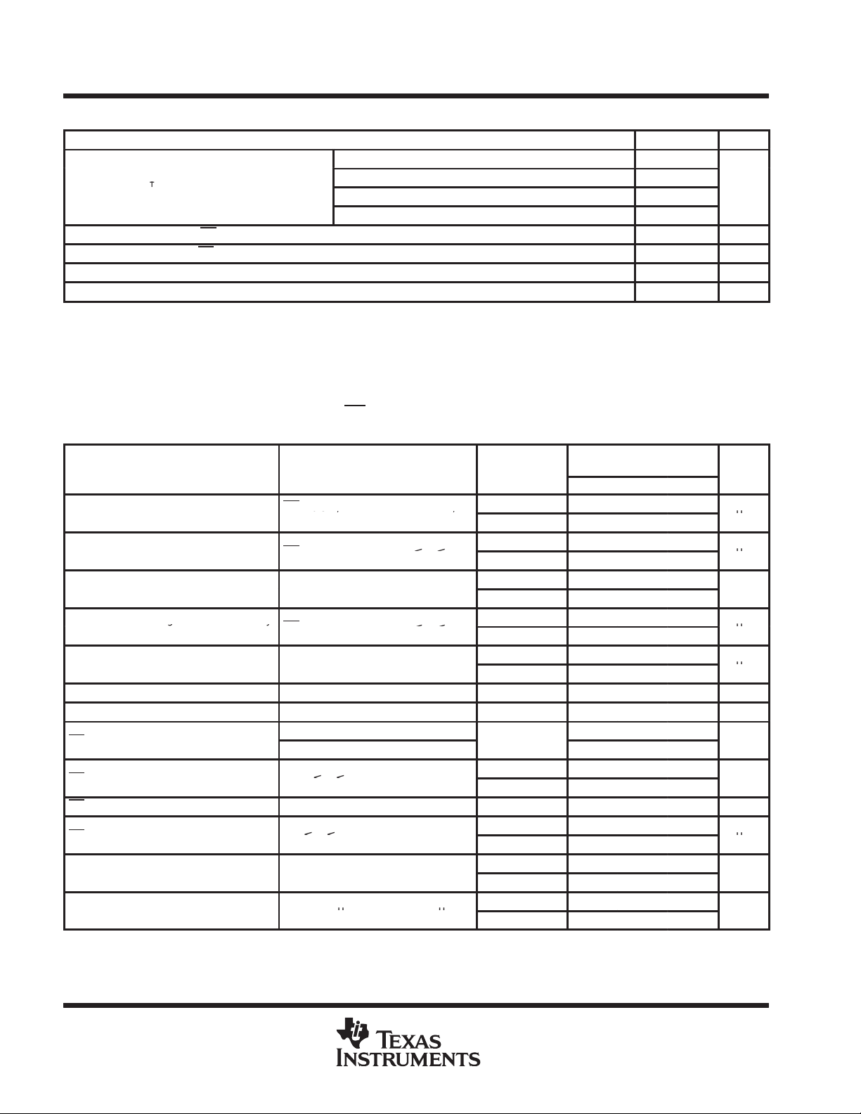
DISSIPATION DERATING CURVE
vs
FREE-AIR TEMPERATURE
1400
1200
1000
800
600
400
200
– Maximum Continuous Dissipation – mW
D
P
0
25 50 75 100
PWP Package
R
= 178°C/W
θJA
TA – Free-Air Temperature – ° C
Figure 3
†
125 150
MAXIMUM CONTINUOUS DISSIPATION
†
vs
CASE TEMPERATURE
30
25
20
PWP Package
15
10
Measured with the exposed thermal pad
coupled to an infinite heat sink with a
5
– Maximum Continuous Dissipation – W
D
P
thermally conductive compound (the
thermal conductivity of the compound
is 0.815 W/m ⋅°C). The R
0
25 50 75 100
TC – Case Temperature – °C
θJC
is 3.5°C/W.
125 150
Figure 4
†
Dissipation rating tables and figures are provided for maintenance of junction temperature at or below absolute maximum temperature of 150°C.
For guidelines on maintaining junction temperature within recommended operating range, see the Thermal Information section.
POST OFFICE BOX 655303 • DALLAS, TEXAS 75265
5
TPS71H01Q, TPS71H33Q, TPS71H48Q, TPS71H50Q
Input voltage, V
†
V
§
J
,
,
Ground current (active mode)
EN ≤ 0.5 V, V
I
V
O
V,
A
Input current (standby mode)
EN
V
2.7 V ≤ V
≤ 10 V
A
Output current limit
V
V
V
A
gy
EN
V
2.7 V ≤ V
V
A
PG leak
t
Normal operation
V
10 V
A
EN logic high (standb
)
40°C to 125°C
V
EN logic l
)
2.7 V ≤ V
V
V
EN i
t
0 V ≤ V
V
A
Minimum V
for active pass element
V
Minimum V
for valid PG
I
300 µA
I
300 µA
V
LOW-DROPOUT VOLTAGE REGULATORS
SLVS152A – NOVEMBER 1996 – REVISED JANUAR Y 1997
recommended operating conditions
MIN MAX UNIT
TPS71H01Q 2.5 10
p
High-level input voltage at EN, V
Low-level input voltage at EN, V
Output current range, I
Operating virtual junction temperature range, T
†
Minimum input voltage defined in the recommended operating conditions is the maximum specified output voltage plus dropout voltage at the
maximum specified load range. Since dropout voltage is a function of output current, the usable range can be extended for lighter loads. To
calculate the minimum input voltage for your maximum output current, use the following equation: V
Because the TPS71H01 is programmable, r
calculating VDO from r
the recommended input voltage range for the TPS71H01.
I
IH
IL
O
is given in Note 2 in the electrical characteristics table. The minimum value of 2.5 V is the absolute lower limit for
DS(on)
DS(on)
electrical characteristics at IO = 10 mA, EN = 0 V , CO = 4.7 µF/CSR‡ = 1 Ω, SENSE/FB shorted to OUT
(unless otherwise noted)
PARAMETER
EN ≤ 0.5 V
0 mA ≤ IO ≤ 500 mA
p
p
Pass-element leakage current in standby
mode
age curren
Output voltage temperature coefficient –40°C to 125°C 61 75 ppm/°C
Thermal shutdown junction temperature 165 °C
y mode
ow (active mode
EN hysteresis voltage 25°C 50 mV
nput curren
I
I
‡
CSR (compensation series resistance) refers to the total series resistance, including the equivalent series resistance (ESR) of the capacitor, any
series resistance added externally, and PWB trace resistance to CO.
§
Pulse-testing techniques are used to maintain virtual junction temperature as close as possible to ambient temperature; thermal effects must
be taken into account separately.
p
O
2.5 V ≤ VI ≤ 6 V
6 V ≤ VI ≤ 10 V
PG
TPS71H33Q 3.77 10
TPS71H48Q 5.2 10
TPS71H50Q 5.33 10
2 V
0.5 V
0 500 mA
J
= V
should be used to calculate VDO before applying the above equation. The equation for
TEST CONDITIONS
=
,
I
= 0,
=
,
I
p
≤ 10
I
≤ 10
I
=
V
= V
+ 1 V
+ 1
I
= 10
I
≤ 10
I
,
=
PG
=
PG
T
25°C 285 350
–40°C to 125°C 460
25°C 0.5
–40°C to 125°C 2
25°C 1.2 2
–40°C to 125°C 2
25°C 0.5
–40°C to 125°C 1
25°C 0.02 0.5
–40°C to 125°C 0.5
°
–
25°C 0.5
–40°C to 125°C 0.5
25°C –0.5 0.5
–40°C to 125°C –0.5 0.5
25°C 2.05 2.5
–40°C to 125°C 2.5
25°C 1.06 1.5
–40°C to 125°C 1.9
I(min)
TPS71H01Q, TPS71H33Q
TPS71H48Q, TPS71H50Q
MIN TYP MAX
°
2
2.7
–40 125 °C
+ V
O(max)
DO(max load)
UNIT
µ
µ
µ
µ
µ
6
POST OFFICE BOX 655303 • DALLAS, TEXAS 75265
PARAMETER
TEST CONDITIONS
‡
T
UNIT
Reference voltage (measured at
V
50 µA ≤ I
150 mA
V
150 mA ≤ I
500 mA
Ω
V
2.9 V
50 µA ≤ I
≤ 500 mA
Input regulation
I
,
µ
O
,
mV
O
,
I
,
mV
Output regulation
O
µ ,
I
,
mV
I
A
Ripple rejection
f
120 H
dB
O
,
†
CSR
†
Ω
PG
§
I
400 µA
V
V
V
FB input current
nA
TPS71H01Q, TPS71H33Q, TPS71H48Q, TPS71H50Q
LOW-DROPOUT VOLTAGE REGULATORS
SLVS152A – NOVEMBER 1996 – REVISED JANUAR Y 1997
TPS71H01 electrical characteristics at IO = 10 mA, V
= 3.5 V, EN = 0 V, CO = 4.7 µF/CSR† = 1 Ω, FB
I
shorted to OUT at device leads (unless otherwise noted)
J
VI = 3.5 V, IO = 10 mA 25°C 1.178 V
FB with OUT connected to FB)
Reference voltage temperature
coefficient
Pass-element series resistance
(see Note 2)
p
p
pp
Output noise-spectral density f = 120 Hz 25°C 2
Output noise voltage
PG trip-threshold voltage
PG hysteresis voltage
p
output low voltage
p
†
CSR refers to the total series resistance, including the ESR of the capacitor, any series resistance added externally, and PWB trace resistance
to CO.
‡
Pulse-testing techniques are used to maintain virtual junction temperature as close as possible to ambient temperature; thermal effects must
be taken into account separately.
§
Output voltage programmed to 2.5 V with closed-loop configuration (see application information).
NOTES: 1. When VI < 2.9 V and IO > 150 mA simultaneously, pass element r
dropout voltage prevents the regulator from maintaining the specified tolerance range.
2. To calculate dropout voltage, use equation:
r
DS(on)
5.9 V , which corresponds to dropout conditions for programmed output voltages of 2.5 V, 3 V, 4 V, and 6 V, respectively. (For other
programmed values, see Figure 26.)
§
§
VDO = IO
⋅ r
is a function of both output current and input voltage. The parametric table lists r
2.5 V ≤ VI ≤ 10 V,
See Note 1
= 2.4 V,
I
= 2.4 V,
I
,
=
I
VI = 3.9 V, 50 µA ≤ IO ≤ 500 mA 25°C 0.32
VI = 5.9 V, 50 µA ≤ IO ≤ 500 mA 25°C 0.23
V
= 2.5 V to 10 V, 50 µA ≤ I
See Note 1
I
= 5 mA to 500 mA, 2.5 V ≤ V
See Note 1
I
= 50 µA to 500 mA, 2.5 V ≤ V
See Note 1
=
10 Hz ≤ f ≤ 100 kHz,
VFB voltage decreasing from above V
Measured at V
PG
DS(on)
=
z
= 1
FB
,
5 mA ≤ IO ≤ 500 mA,
≤
O
≤
O
O
≤ 500 mA,
≤ 10 V,
≤ 10 V,
= 50 µ
O
I
= 500 mA,
See Note 1
CO = 4.7 µF 25°C 95
CO = 10 µF 25°C 89
CO = 100 µF 25°C 74
PG
= 2.13
I
DS(on)
–40°C to 125°C 1.143 1.213 V
–40°C to 125°C 61 75 ppm/°C
25°C 0.7 1
–40°C to 125°C 1
25°C 0.83 1.3
–40°C to 125°C 1.3
25°C 0.52 0.85
–40°C to 125°C 0.85
25°C 18
–40°C to 125°C 25
25°C 14
–40°C to 125°C 25
25°C 22
–40°C to 125°C 54
25°C 48 59
–40°C to 125°C 44
25°C 45 54
–40°C to 125°C 44
–40°C to 125°C 1.101 1.145 V
25°C 12 mV
25°C 0.1 0.4
–40°C to 125°C 0.4
25°C –10 0.1 10
–40°C to 125°C –20 20
increases (see Figure 27) to a point such that the resulting
DS(on)
TPS71H01Q
MIN TYP MAX
µV/√Hz
µVrms
for VI = 2.4 V, 2.9 V, 3.9 V, and
POST OFFICE BOX 655303 • DALLAS, TEXAS 75265
7
TPS71H01Q, TPS71H33Q, TPS71H48Q, TPS71H50Q
PARAMETER
TEST CONDITIONS
‡
T
UNIT
Output voltage
V
I
V
V
D
I
100 mA
V
V
mV
I
500 mA
V
3.23 V
(
O)O
,
I
,
Ω
Input regulation
V
50 µA ≤ I
500 mA
mV
I
5 mA to 500 mA
V
≤ 10 V
mV
Output regulation
I
500 mA
V
V
mV
I
A
Ripple rejection
f
120 H
dB
I
500 mA
CSR
†
Ω
PG output low voltage
I
V
V
V
LOW-DROPOUT VOLTAGE REGULATORS
SLVS152A – NOVEMBER 1996 – REVISED JANUAR Y 1997
TPS71H33 electrical characteristics at IO = 10 mA, V
= 4.3 V , EN = 0 V , CO = 4.7 µF/CSR† = 1 Ω, SENSE
I
shorted to OUT (unless otherwise noted)
J
p
ropout voltage
Pass-element series (3.23 V – V
resistance
p
p
pp
Output noise-spectral density f = 120 Hz 25°C 2
Output noise voltage
PG trip-threshold voltage
PG hysteresis voltage
p
†
CSR refers to the total series resistance, including the ESR of the capacitor, any series resistance added externally, and PWB trace resistance
to CO.
‡
Pulse-testing techniques are used to maintain virtual junction temperature as close as possible to ambient temperature; thermal effects must
be taken into account separately.
VI = 4.3 V, IO = 10 mA 25°C 3.3
4.3 V ≤ VI ≤ 10 V, 5 mA ≤ IO ≤ 500 mA –40°C to 125°C 3.23 3.37
= 10 mA,
O
=
O
=
O
IO = 500 mA
= 4.3 V to 10 V,
I
=
O
= 50 µA to
O
=
10 Hz ≤ f ≤ 100 kHz,
VO voltage decreasing from above V
= 1 mA,
PG
†
= 1
=
,
,
)/I
, V
z
= 3.23
I
= 3.23
I
=
I
= 3.23 V,
,4.3 V ≤
,4.3 V ≤
= 50 µ
O
=
O
CO = 4.7 µF
CO = 10 µF
CO = 100 µF
= 2.8
I
O
I
I
≤
≤ 10
PG
25°C 4.5 7
–40°C to 125°C 8
25°C 47 60
–40°C to 125°C 80
25°C 235 300
–40°C to 125°C 400
25°C 0.47 0.6
–40°C to 125°C 0.8
25°C 20
–40°C to 125°C 27
25°C 21 38
–40°C to 125°C 75
25°C 30 60
–40°C to 125°C 120
25°C 43 54
–40°C to 125°C 40
25°C 39 49
–40°C to 125°C 36
25°C 274
25°C 228
25°C 159
–40°C to 125°C 2.868 3 V
25°C 35 mV
25°C 0.22 0.4
–40°C to 125°C 0.4
TPS71H33Q
MIN TYP MAX
µV/√Hz
µVrms
8
POST OFFICE BOX 655303 • DALLAS, TEXAS 75265
PARAMETER
TEST CONDITIONS
‡
T
UNIT
Output voltage
V
I
V
V
D
I
100 mA
V
V
mV
I
500 mA
V
V
(
O)O
,
I
,
Ω
Input regulation
V
50 µA ≤ I
500 mA
mV
I
500 mA
V
V
mV
Output regulation
I
50 µA to 500 mA
V
≤ 10 V
mV
I
A
Ripple rejection
f
120 H
dB
I
500 mA
CSR
†
Ω
PG
I
V
V
V
TPS71H01Q, TPS71H33Q, TPS71H48Q, TPS71H50Q
LOW-DROPOUT VOLTAGE REGULATORS
SLVS152A – NOVEMBER 1996 – REVISED JANUAR Y 1997
TPS71H48 electrical characteristics at IO = 10 mA, V
= 5.85 V, EN = 0 V, CO = 4.7 µF/CSR† = 1 Ω,
I
SENSE shorted to OUT (unless otherwise noted)
J
p
ropout voltage
Pass-element series (4.75 V – V
resistance
p
p
pp
Output noise-spectral density f = 120 Hz 25°C 2 µV/√Hz
Output noise voltage
PG trip-threshold voltage
PG hysteresis voltage
output low voltage
†
CSR refers to the total series resistance, including the ESR of the capacitor, any series resistance added externally, and PWB trace resistance
to CO.
‡
Pulse-testing techniques are used to maintain virtual junction temperature as close as possible to ambient temperature; thermal effects must
be taken into account separately.
VI = 5.85 V, IO = 10 mA 25°C 4.85
5.85 V ≤ VI ≤ 10 V, 5 mA ≤ IO ≤ 500 mA –40°C to 125°C 4.75 4.95
= 10 mA,
O
=
O
=
O
IO = 500 mA
= 5.85 V to 10 V,
I
= 5 mA to
O
=
O
=
10 Hz ≤ f ≤ 100 kHz,
VO voltage decreasing from above V
= 1.2 mA,
PG
†
= 1
=
,
,
)/I
, V
z
= 4.75
I
= 4.75
I
= 4.75
I
= 4.75 V,
,5.85 V ≤
,5.85 V ≤
= 50 µ
O
=
O
CO = 4.7 µF
CO = 10 µF
CO = 100 µF
= 4.12
I
O
≤
≤ 10
I
I
PG
25°C 2.9 6
–40°C to 125°C 8
25°C 30 37
–40°C to 125°C 54
25°C 150 180
–40°C to 125°C 250
25°C 0.32 0.35
–40°C to 125°C 0.52
25°C 27
–40°C to 125°C 37
25°C 12 42
–40°C to 125°C 80
25°C 42 60
–40°C to 125°C 130
25°C 42 53
–40°C to 125°C 39
25°C 39 50
–40°C to 125°C 35
25°C 410
25°C 328
25°C 212
–40°C to 125°C 4.5 4.7 V
25°C 50 mV
25°C 0.2 0.4
–40°C to 125°C 0.4
TPS71H48Q
MIN TYP MAX
µVrms
POST OFFICE BOX 655303 • DALLAS, TEXAS 75265
9
TPS71H01Q, TPS71H33Q, TPS71H48Q, TPS71H50Q
PARAMETER
TEST CONDITIONS
‡
T
UNIT
Output voltage
V
I
V
V
D
I
100 mA
V
V
mV
I
500 mA
V
V
(
O)O
,
I
Ω
Input regulation
V
50 µA ≤ I
500 mA
mV
I
500 mA
V
V
mV
Output regulation
I
50 µA to 500 mA
V
≤ 10 V
mV
I
A
Ripple rejection
f
120 H
dB
I
500 mA
CSR
†
Ω
PG output low voltage
I
V
V
V
LOW-DROPOUT VOLTAGE REGULATORS
SLVS152A – NOVEMBER 1996 – REVISED JANUAR Y 1997
TPS71H50 electrical characteristics at IO = 10 mA, V
= 6 V , EN = 0 V , CO = 4.7 µF/CSR† = 1 Ω, SENSE
I
shorted to OUT (unless otherwise noted)
J
p
ropout voltage
Pass-element series (4.88 V – V
resistance
p
p
pp
Output noise-spectral density f = 120 Hz 25°C 2
Output noise voltage
PG trip-threshold voltage
PG hysteresis voltage
p
†
CSR refers to the total series resistance, including the ESR of the capacitor, any series resistance added externally, and PWB trace resistance
to CO.
‡
Pulse-testing techniques are used to maintain virtual junction temperature as close as possible to ambient temperature; thermal effects must
be taken into account separately.
VI = 6 V, IO = 10 mA 25°C 5
6 V ≤ VI ≤ 10 V, 5 mA ≤ IO ≤ 500 mA –40°C to 125°C 4.9 5.1
= 10 mA,
O
=
O
=
O
IO = 500 mA
= 6 V to 10 V,
I
= 5 mA to
O
=
O
=
10 Hz ≤ f ≤ 100 kHz,
VO voltage decreasing from above V
= 1.2 mA,
PG
†
= 1
=
,
,
)/I
, V
z
= 4.88
I
= 4.88
I
= 4.88
I
= 4.88 V.
,6 V ≤
,6 V ≤
= 50 µ
O
=
O
CO = 4.7 µF
CO = 10 µF
CO = 100 µF
= 4.25
I
O
≤ 10
I
I
≤
PG
25°C 2.9 6
–40°C to 125°C 8
25°C 27 32
–40°C to 125°C 47
25°C 146 170
–40°C to 125°C 230
25°C 0.29 0.32
–40°C to 125°C 0.47
25°C 25
–40°C to 125°C 32
25°C 30 45
–40°C to 125°C 86
25°C 45 65
–40°C to 125°C 140
25°C 45 55
–40°C to 125°C 40
25°C 42 52
–40°C to 125°C 36
25°C 430
25°C 345
25°C 220
–40°C to 125°C 4.55 4.75 V
25°C 53 mV
25°C 0.2 0.4
–40°C to 125°C 0.4
TPS71H50Q
MIN TYP MAX
µV/√Hz
µVrms
10
POST OFFICE BOX 655303 • DALLAS, TEXAS 75265

VOOutput voltage
rrent
Ripple rejection
Frequenc
Output spectral noise densit
s
Freq
enc
V
CSR
Compensation series resistance
rrent
CSR
Compensation series resistance
Ceramic capacitance
CSR
Compensation series resistance
rrent
CSR
Compensation series resistance
Ceramic capacitance
TPS71H01Q, TPS71H33Q, TPS71H48Q, TPS71H50Q
LOW-DROPOUT VOLTAGE REGULATORS
SLVS152A – NOVEMBER 1996 – REVISED JANUAR Y 1997
TYPICAL CHARACTERISTICS
Table of Graphs
FIGURE
vs Output current 5
I
Q
V
DO
∆V
DO
∆V
O
V
O
∆V
O
r
DS(on)
R Divider resistance vs Free-air temperature 26
I
I(SENSE)
I
I
I(EN)
V
PG
Quiescent current
Typical dropout voltage vs Output current 8
Change in dropout voltage vs Free-air temperature 9
Change in output voltage vs Free-air temperature 10
Output voltage vs Input voltage 11
Change in output voltage vs Input voltage 12
p
pp
p
p
Pass-element resistance vs Input voltage 25
SENSE current vs Free-air temperature 27
FB leakage current vs Free-air temperature 28
Minimum input voltage for active-pass element vs Free-air temperature 29
Minimum input voltage for valid PG vs Free-air temperature 30
Input current (EN) vs Free-air temperature 31
Output voltage response from Enable (EN) 32
Power-good (PG) voltage vs Output voltage 33
p
p
p
p
yv
vs Input voltage 6
vs Free-air temperature 7
13
p
vs Output cu
vs
vs Output cu
vs
vs Output cu
vs
y
u
y
p
p
p
p
14
15
16
17
18
19
20
21
22
23
24
34
35
36
37
38
39
40
41
POST OFFICE BOX 655303 • DALLAS, TEXAS 75265
11
TPS71H01Q, TPS71H33Q, TPS71H48Q, TPS71H50Q
LOW-DROPOUT VOLTAGE REGULATORS
SLVS152A – NOVEMBER 1996 – REVISED JANUAR Y 1997
TYPICAL CHARACTERISTICS
355
TA = 25°C
345
335
Aµ
– Quiescent Current –
Q
I
TPS71Hxx, VI = 10 V
325
315
305
295
TPS71H50, VI = 6 V
285
TPS71H48, VI = 5.85 V
275
TPS71H33, VI = 4.3 V
265
0 50 100 150 200 250 300
FREE-AIR TEMPERATURE
400
VI = V
O(nom)
IO = 10 mA
350
Aµ
300
250
– Quiesent Current –
Q
I
200
QUIESCENT CURRENT
vs
OUTPUT CURRENT
350 400 450 500
IO – Output Current – mA
Figure 5
TPS71H48Q
QUIESCENT CURRENT
vs
+ 1 V
QUIESCENT CURRENT
INPUT VOLTAGE
400
TA = 25°C
RL = 10 Ω
350
Aµ
300
250
200
150
– Quiescent Current –
Q
100
I
50
0
0123456
TPS71H33
VI – Input Voltage – V
Figure 6
DROPOUT VOLTAGE
OUTPUT CURRENT
0.3
TA = 25°C
0.25
0.2
0.15
Dropout Voltage – V
0.1
0.05
vs
TPS71H48
TPS71H50
TPS71H01 With V
Programmed to 2.5 V
O
78910
vs
TPS71H33
TPS71H48
TPS71H50
12
150
–50 –25 0 25 50 75 100 125
TA – Free-Air Temperature – ° C
Figure 7
POST OFFICE BOX 655303 • DALLAS, TEXAS 75265
0
0 50 100 150 200 250 300
IO – Output Current – mA
Figure 8
350 400 450 500

TPS71H01Q, TPS71H33Q, TPS71H48Q, TPS71H50Q
LOW-DROPOUT VOLTAGE REGULATORS
SLVS152A – NOVEMBER 1996 – REVISED JANUAR Y 1997
TYPICAL CHARACTERISTICS
CHANGE IN DROPOUT VOLTAGE
vs
FREE-AIR TEMPERATURE
10
IO = 100 mA
8
6
4
2
0
–2
–4
–6
Change in Dropout Voltage – mV
–8
–10
–50 –25 0 25 50 75 100 125
TA – Free-Air Temperature – ° C
Figure 9
OUTPUT VOLTAGE
vs
INPUT VOLTAGE
6
TA = 25°C
RL = 10 Ω
5
4
3
TPS71H50
TPS71H48
TPS71H33
CHANGE IN OUTPUT VOLTAGE
vs
FREE-AIR TEMPERATURE
20
VI = V
IO = 10 mA
15
10
5
0
–5
–10
– Change in Output Voltage – mV
O
V
–15
∆
–20
–50 –25 0 25 50 75 100 125
+ 1 V
O(nom)
TA – Free-Air Temperature – ° C
Figure 10
CHANGE IN OUTPUT VOLTAGE
vs
INPUT VOLTAGE
20
TA = 25°C
RL = 10 Ω
15
10
5
0
TPS71H50
TPS71H48
2
– Output Voltage – V
O
V
1
0
TPS71H01 With V
Programmed to 2.5 V
0123456
VI – Input Voltage – V
Figure 11
O
78910
POST OFFICE BOX 655303 • DALLAS, TEXAS 75265
–5
–10
– Change In Output Voltage – mV
O
∆V
–15
–20
TPS71H33
4567
VI – Input Voltage – V
Figure 12
8910
13
TPS71H01Q, TPS71H33Q, TPS71H48Q, TPS71H50Q
LOW-DROPOUT VOLTAGE REGULATORS
SLVS152A – NOVEMBER 1996 – REVISED JANUAR Y 1997
TYPICAL CHARACTERISTICS
OUTPUT VOLTAGE
OUTPUT CURRENT
2.52
TA = 25°C
2.515
2.505
2.495
– Output Voltage – V
O
V
2.485
VO Programmed to 2.5 V
2.51
2.5
VI = 10 V
2.49
2.48
0 100 200 300
VI = 3.5 V
IO – Output Current – mA
TPS71H01Q
vs
Figure 13
400 500
OUTPUT VOLTAGE
OUTPUT CURRENT
3.34
TA = 25°C
3.33
3.32
3.31
3.3
3.29
– Output Voltage – V
O
V
3.28
3.27
3.26
0 100 200 300
VI = 4.3 V
IO – Output Current – mA
Figure 14
TPS71H33Q
vs
VI = 10 V
400 500
OUTPUT VOLTAGE
OUTPUT CURRENT
4.92
TA = 25°C
4.91
4.9
4.89
4.88
4.87
4.86
4.85
– Output Voltage – V
4.84
O
V
4.83
4.82
4.81
4.8
0 100 300
IO – Output Current – mA
TPS71H48Q
vs
VI = 5.85 V
VI = 10 V
200 400
Figure 15
500
OUTPUT VOLTAGE
OUTPUT CURRENT
5.06
5.05
5.04
5.03
5.02
5.01
4.99
– Output Voltage – V
4.98
O
V
4.97
4.96
4.95
4.94
TA = 25°C
5
VI = 10 V
0 100 300
IO – Output Current – mA
Figure 16
TPS71H50Q
vs
VI = 6 V
200
400 500
14
POST OFFICE BOX 655303 • DALLAS, TEXAS 75265

TPS71H01Q, TPS71H33Q, TPS71H48Q, TPS71H50Q
LOW-DROPOUT VOLTAGE REGULATORS
SLVS152A – NOVEMBER 1996 – REVISED JANUAR Y 1997
TYPICAL CHARACTERISTICS
TPS71H01Q
RIPPLE REJECTION
vs
FREQUENCY
70
60
50
40
30
TA = 25°C
Ripple Rejection – dB
VI = 3.5 V
20
CO = 4.7 µF (CSR = 1 Ω)
No Input Capacitance
VO Programmed to 2.5 V
10
0
10 100 1K 10K 100K 1M 10M
RL = 10 Ω
f – Frequency – Hz
RL = 100 kΩ
RL = 500 Ω
Figure 17
70
60
50
40
30
20
Ripple Rejection – dB
TA = 25°C
10
VI = 3.5 V
CO = 4.7 µF (CSR = 1 Ω)
0
No Input Capacitance
–10
10
TPS71H33Q
RIPPLE REJECTION
vs
FREQUENCY
RL = 100 kΩ
RL = 500 Ω
RL = 10 Ω
10 M1 M100 k10 k1 k100
f – Frequency – Hz
Figure 18
70
60
50
40
30
20
Ripple Rejection – dB
10
–10
RL = 10 Ω
TA = 25°C
VI = 3.5 V
0
CO = 4.7 µF (CSR = 1 Ω)
No Input Capacitance
10
TPS71H48Q
RIPPLE REJECTION
vs
FREQUENCY
RL = 100 kΩ
RL = 500 Ω
f – Frequency – Hz
Figure 19
TPS71H50Q
RIPPLE REJECTION
vs
FREQUENCY
70
60
50
RL = 10 Ω
40
30
Ripple Rejection – dB
20
TA = 25°C
VI = 3.5 V
10
CO = 4.7 µF (CSR = 1 Ω)
No Input Capacitance
10 M1 M100 k10 k1 k100
0
10
f – Frequency – Hz
RL = 100 kΩ
RL = 500 Ω
10 M1 M100 k10 k1 k100
Figure 20
POST OFFICE BOX 655303 • DALLAS, TEXAS 75265
15

TPS71H01Q, TPS71H33Q, TPS71H48Q, TPS71H50Q
LOW-DROPOUT VOLTAGE REGULATORS
SLVS152A – NOVEMBER 1996 – REVISED JANUAR Y 1997
TYPICAL CHARACTERISTICS
TPS71H01Q
OUTPUT SPECTRAL NOISE DENSITY
FREQUENCY
10
Hzµ
V/
1
0.1
Output Spectral Noise Density –
CO = 100 µF (CSR = 1 Ω)
0.01
10 10
2
f – Frequency – Hz
Figure 21
vs
TA = 25°C
No Input Capacitance
VI = 3.5 V
VO Programmed to 2.5 V
CO = 4.7 µF (CSR = 1 Ω)
CO = 10 µF (CSR = 1 Ω)
10
3
10
4
10
TPS71H33Q
OUTPUT SPECTRAL NOISE DENSITY
vs
FREQUENCY
10
Hzµ
V/
1
0.1
Output Spectral Noise Density –
5
0.01
10
2
10
f – Frequency – Hz
TA = 25°C
No Input Capacitance
VI = 4.3 V
CO = 10 µF (CSR = 1 Ω)
CO = 4.7 µF (CSR = 1 Ω)
CO = 100 µF (CSR = 1 Ω)
10
3
10
4
10
5
Figure 22
TPS71H48Q
OUTPUT SPECTRAL NOISE DENSITY
vs
FREQUENCY
10
V/ Hzµ
1
0.1
CO = 100 µF (CSR = 1 Ω)
Output Spectral Noise Density –
0.01
10 100 1 k 10 k 100 k
f – Frequency – Hz
TA = 25°C
No Input Capacitance
VI = 5.85 V
CO = 10 µF (CSR = 1 Ω)
CO = 4.7 µF (CSR = 1 Ω)
Figure 23
TPS71H50Q
OUTPUT SPECTRAL NOISE DENSITY
vs
FREQUENCY
10
Hzµ
V/
1
0.1
Output Spectral Noise Density –
CO = 100 µF (CSR = 1 Ω)
0.01
10 100 1 k 10 k 100 k
CO = 10 µF (CSR = 1 Ω)
CO = 4.7 µF (CSR = 1 Ω)
TA = 25°C
No Input Capacitance
VI = 6 V
f – Frequency – Hz
Figure 24
16
POST OFFICE BOX 655303 • DALLAS, TEXAS 75265

TPS71H01Q, TPS71H33Q, TPS71H48Q, TPS71H50Q
LOW-DROPOUT VOLTAGE REGULATORS
SLVS152A – NOVEMBER 1996 – REVISED JANUAR Y 1997
TYPICAL CHARACTERISTICS
PASS-ELEMENT RESISTANCE
vs
INPUT VOLTAGE
1.1
1
Ω
0.9
0.8
0.7
0.6
0.5
0.4
– Pass-Element Resistance –
0.3
DS(on)
r
0.2
0.1
2457
368
IO = 500 mA
IO = 100 mA
VI – Input Voltage – V
Figure 25
FIXED-OUTPUT VERSIONS
SENSE PIN CURRENT
vs
FREE-AIR TEMPERATURE
6
VI = V
V
I(sense)
5.8
Aµ
5.6
O(nom)
= V
+ 1 V
O(nom)
T
= 25°C
A
V
= 1.12 V
I(FB)
910
DIVIDER RESISTANCE
vs
FREE-AIR TEMPERATURE
1.2
1.1
Ω
1
0.9
0.8
0.7
0.6
R – Divider Resistance – M
0.5
0.4
–50 –25 0 25 50 75 100 125
TPS71H50
TPS71H48
TPS71H33
TA – Free-Air Temperature – ° C
VI = V
V
I(sense)
O(nom)
= V
Figure 26
ADJUSTABLE VERSION
FB LEAKAGE CURRENT
vs
FREE-AIR TEMPERATURE
0.6
VFB = 2.5 V
0.5
+ 1 V
O(nom)
5.4
5.2
5
– Sense Pin Current –
4.8
I(sense)
I
4.6
4.4
–50 –25 0 25 50 75 100 125
TA – Free-Air Temperature – ° C
Figure 27
POST OFFICE BOX 655303 • DALLAS, TEXAS 75265
0.4
0.3
0.2
FB Leakage Current – nA
0.1
0
–50 –25 0 25 50 75 100 125
TA – Free-Air Temperature – ° C
Figure 28
17

TPS71H01Q, TPS71H33Q, TPS71H48Q, TPS71H50Q
LOW-DROPOUT VOLTAGE REGULATORS
SLVS152A – NOVEMBER 1996 – REVISED JANUAR Y 1997
TYPICAL CHARACTERISTICS
MINIMUM INPUT VOLTAGE FOR ACTIVE
PASS ELEMENT
vs
FREE-AIR TEMPERATURE
2.1
RL = 500 Ω
2.09
2.08
2.07
2.06
2.05
2.04
2.03
– Minimum Input Voltage – V
I
2.02
V
2.01
2
–50 –25 0 25 50 75 100 125
TA – Free-Air Temperature – ° C
Figure 29
MINIMUM INPUT VOLTAGE FOR VALID
POWER GOOD (PG)
vs
FREE-AIR TEMPERATURE
1.1
1.09
1.08
1.07
– Minimum Input Voltage – V
I
V
1.06
1.05
–50 –25 0 25 50 75 100 125
TA – Free-Air Temperature – ° C
Figure 30
EN INPUT CURRENT
vs
FREE-AIR TEMPERATURE
100
VI = V
90
80
70
60
50
40
– Input Current – nA
30
I(EN)
I
20
10
0
–40 –20 0 20 40 60 80 100 120 140
= 10 V
I(EN)
TA – Free-Air Temperature – ° C
Figure 31
18
POST OFFICE BOX 655303 • DALLAS, TEXAS 75265

TPS71H01Q, TPS71H33Q, TPS71H48Q, TPS71H50Q
LOW-DROPOUT VOLTAGE REGULATORS
SLVS152A – NOVEMBER 1996 – REVISED JANUAR Y 1997
TYPICAL CHARACTERISTICS
OUTPUT VOLTAGE RESPONSE FROM
– Output Voltage – V
O
V
ENABLE (EN
V
O(nom)
TA = 25°C
RL = 500 Ω
CO = 4.7 µF (ESR = 1Ω)
No Input Capacitance
)
6
4
2
EN Voltage – V
0
0 20 40 60 80 100 120 140
Time – µs
Figure 32
POWER-GOOD (PG) VOLTAGE
vs
OUTPUT VOLTAGE
6
TA = 25°C
PG Pulled Up to 5 V With 5 kΩ
5
4
3
2
– Power-Good (PG) Voltage – V
PG
1
V
0
93 94 95 96
VO – Output Voltage (VO as a percent of V
Figure 33
97 98
) – %
O(nom)
–2
POST OFFICE BOX 655303 • DALLAS, TEXAS 75265
19

TPS71H01Q, TPS71H33Q, TPS71H48Q, TPS71H50Q
LOW-DROPOUT VOLTAGE REGULATORS
SLVS152A – NOVEMBER 1996 – REVISED JANUAR Y 1997
TYPICAL CHARACTERISTICS
TYPICAL REGIONS OF STABILITY
COMPENSATION SERIES RESISTANCE
OUTPUT CURRENT
100
Compensation Series Resistance – Ω
CSR –
0.1
VI = V
O(nom)
No Input Capacitance
CO = 4.7 µF
No Added Ceramic Capacitance
TA = 25°C
10
1
0 50 100 150 200 250 300
IO – Output Current – mA
Figure 34
+ 1 V
vs
Region of Instability
Region of Instability
350 400 450 500
TYPICAL REGIONS OF STABILITY
COMPENSATION SERIES RESISTANCE
vs
OUTPUT CURRENT
100
VI = V
No Input Capacitance
CO = 4.7 µF + 0.5 µF of
Ceramic Capacitance
TA = 25°C
10
1
Compensation Series Resistance – ΩCSR –
0.1
0 50 100 150 200 250 300 350 400 450 500
+ 1 V
O(nom)
Region of Instability
Region of Instability
IO – Output Current – mA
Figure 35
TYPICAL REGIONS OF STABILITY
COMPENSATION SERIES RESISTANCE
vs
ADDED CERAMIC CAPACITANCE
100
VI = V
No Input Capacitance
IO= 100 mA
CO = 4.7 µF
TA = 25°C
10
1
Compensation Series Resistance – ΩCSR –
0.1
0 0.1 0.2 0.3 0.4 0.5 0.6 0.7 0.8 0.9 1
+ 1 V
O(nom)
Region of Instability
Region of Instability
Ceramic Capacitance – µF
Figure 36
TYPICAL REGIONS OF STABILITY
COMPENSATION SERIES RESISTANCE
vs
ADDED CERAMIC CAPACITANCE
100
VI = V
No Input Capacitance
IO= 500 mA
CO = 4.7 µF
TA = 25°C
10
1
Compensation Series Resistance – ΩCSR –
0.1
0 0.1 0.2 0.3 0.4 0.5 0.6 0.7 0.8 0.9 1
+ 1 V
O(nom)
Region of Instability
Region of Instability
Ceramic Capacitance – µF
Figure 37
20
POST OFFICE BOX 655303 • DALLAS, TEXAS 75265

TPS71H01Q, TPS71H33Q, TPS71H48Q, TPS71H50Q
LOW-DROPOUT VOLTAGE REGULATORS
SLVS152A – NOVEMBER 1996 – REVISED JANUAR Y 1997
TYPICAL CHARACTERISTICS
TYPICAL REGIONS OF STABILITY
COMPENSATION SERIES RESISTANCE
OUTPUT CURRENT
100
Region of Instability
10
1
Compensation Series Resistance – ΩCSR –
0.1
0 50 100 150 200 250 300
IO – Output Current – mA
vs
VI = V
O(nom)
No Input Capacitance
CO = 10 µF
No Ceramic Capacitance
TA = 25°C
Figure 38
†
+ 1 V
350 400 450 500
TYPICAL REGIONS OF STABILITY
COMPENSATION SERIES RESISTANCE
OUTPUT CURRENT
100
VI = V
No Input Capacitance
CO = 10 µF + 0.5 µF of
Added Ceramic Capacitance
TA = 25°C
10
1
Compensation Series Resistance – ΩCSR –
0.1
0 50 100 150 200 250 300
+ 1 V
O(nom)
Region of Instability
IO – Output Current – mA
Figure 39
†
vs
350 400 450 500
TYPICAL REGIONS OF STABILITY
COMPENSATION SERIES RESISTANCE
ADDED CERAMIC CAPACITANCE
100
VI = V
No Input Capacitance
CO = 10 µF
IO = 100 mA
TA = 25°C
10
1
Compensation Series Resistance – ΩCSR –
0.1
0 0.1 0.2 0.3 0.4 0.5 0.6
+ 1 V
O(nom)
Region of Instability
Ceramic Capacitance – µF
vs
Figure 40
†
0.7 0.8 0.9 1
TYPICAL REGIONS OF STABILITY
COMPENSATION SERIES RESISTANCE
ADDED CERAMIC CAPACITANCE
100
VI = V
No Input Capacitance
CO = 10 µF
IO = 500 mA
TA = 25°C
10
1
Compensation Series Resistance – ΩCSR –
0.1
0 0.1 0.2 0.3 0.4 0.5 0.6
+ 1 V
O(nom)
Region of Instability
Ceramic Capacitance – µF
Figure 41
†
vs
0.7 0.8 0.9 1
†CSR values below 0.1 Ω are not recommended.
POST OFFICE BOX 655303 • DALLAS, TEXAS 75265
21

TPS71H01Q, TPS71H33Q, TPS71H48Q, TPS71H50Q
LOW-DROPOUT VOLTAGE REGULATORS
SLVS152A – NOVEMBER 1996 – REVISED JANUAR Y 1997
TYPICAL CHARACTERISTICS
+
C
CSR
To Load
O
†
C
cer
R
L
V
I
†
Ceramic capacitor
IN
EN
OUT
SENSE
GND
Figure 42. Test Circuit for Typical Regions of Stability (see Figures 34 through 41)
22
POST OFFICE BOX 655303 • DALLAS, TEXAS 75265

TPS71H01Q, TPS71H33Q, TPS71H48Q, TPS71H50Q
LOW-DROPOUT VOLTAGE REGULATORS
SLVS152A – NOVEMBER 1996 – REVISED JANUAR Y 1997
THERMAL INFORMATION
standard TSSOP-20
In response to system-miniaturization trends, integrated circuits are being offered in low-profile and fine-pitch
surface-mount packages. Implementation of many of today’s high-performance devices in these packages
requires special attention to power dissipation. Many system-dependent issues such as thermal coupling,
airflow, added heat sinks and convection surfaces, and the presence of other heat-generating components
affect the power-dissipation limits of a given component.
Three basic approaches for enhancing thermal performance are illustrated in this discussion:
D
Improving the power-dissipation capability of the PWB design
D
Improving the thermal coupling of the component to the PWB
D
Introducing airflow in the system
Figure 43 is an example of a thermally enhanced PWB layout for the 20-lead TSSOP package. This layout
involves adding copper on the PWB to conduct heat away from the device. The R
system is illustrated in Figure 44. The family of curves illustrates the effect of increasing the size of the
copper-heat-sink surface area. The PWB is a standard FR4 board (L × W × H = 3.2 inch × 3.2 inch × 0.062 inch);
the board traces and heat sink area are 1-oz (per square foot) copper.
for this component/board
θJA
Copper Heat Sink
1 oz Copper
Figure 43. Thermally Enhanced PWB Layout (not to scale) for the 20-Pin TSSOP
Figure 45 shows the thermal resistance for the same system with the addition of a thermally conductive
compound between the body of the TSSOP package and the PWB copper routed directly beneath the device.
The thermal conductivity for the compound used in this analysis is 0.815 W/m × °C.
POST OFFICE BOX 655303 • DALLAS, TEXAS 75265
23

TPS71H01Q, TPS71H33Q, TPS71H48Q, TPS71H50Q
LOW-DROPOUT VOLTAGE REGULATORS
SLVS152A – NOVEMBER 1996 – REVISED JANUAR Y 1997
THERMAL INFORMATION
standard TSSOP-20 (continued)
THERMAL RESISTANCE, JUNCTION-TO-AMBIENT
vs
AIR FLOW
190
C/W
°
170
2
1 cm
150
130
110
90
70
50
JAθ
0 50 100 150 200 250
R – Thermal Resistance, Junction-to-Ambient –
4 cm
Component/Board System
20-Lead TSSOP
2
0 cm
2
2 cm
2
Air Flow – ft/min
8 cm
2
Figure 44
Using these figures to determine the system R
with the equation:
THERMAL RESISTANCE, JUNCTION-TO-AMBIENT
vs
AIR FLOW
190
C/W
Component/Board System
20-Lead TSSOP
170
Includes Thermally Conductive
Compound Between Body and Board
150
130
2
110
90
70
50
JAθ
8 cm
0 50 100 150 200 250
Air Flow – ft/min
4 cm
2
2 cm
2
0 cm
1 cm
2
2
300
°
R – Thermal Resistance, Junction-to-Ambient –
Figure 45
allows the maximum power-dissipation limit to be calculated
θJA
300
P
D(max)
+
T
J(max)
R
q
*
T
JA(system)
A
Where
T
is the maximum allowable junction temperature (i.e., 150°C absolute maximum and
J(max)
125°C maximum recommended operating temperature for specified operation).
This limit should then be applied to the internal power dissipated by the TPS71Hxx regulator. The equation for
calculating total internal power dissipation of the TPS71Hxx is:
P
D(total)
+
ǒ
VI*
Ǔ
V
@
IO)
V
@
I
O
I
Q
Because the quiescent current of the TPS71Hxx family is very low, the second term is negligible, further
simplifying the equation to:
P
D(total)
+
ǒ
VI*
Ǔ
V
@
I
O
O
24
POST OFFICE BOX 655303 • DALLAS, TEXAS 75265

TPS71H01Q, TPS71H33Q, TPS71H48Q, TPS71H50Q
LOW-DROPOUT VOLTAGE REGULATORS
SLVS152A – NOVEMBER 1996 – REVISED JANUAR Y 1997
THERMAL INFORMATION
standard TSSOP-20 (continued)
For a 20-lead TSSOP /FR4 board system with thermally conductive compound between the board and the
device body, where T
power-dissipation limit can be calculated. As indicated in Figure 45, the system R
maximum power-dissipation limit is:
= 55°C, airflow = 100 ft/min, copper heat sink area = 1 cm2, the maximum
A
is 94°C/W; therefore, the
θJA
T
P
D(max)
If the system implements a TPS71H48 regulator where V
is:
P
D(total)
Comparing P
maximum limit. When it does, one of two corrective actions can be taken. The power-dissipation limit can be
raised by increasing the airflow or the heat-sink area. Alternatively , the internal power dissipation of the regulator
can be lowered by reducing the input voltage or the load current. In either case, the above calculations should
be repeated with the new system parameters.
+
ǒ
+
D(total)
J(max)
R
q
VI*
with P
*
T
JA(system)
Ǔ
V
@
IO+(6*
O
D(max)
A
°°
125 C*55 C
+
reveals that the power dissipation in this example does not exceed the
°
94 CńW
4.85)@0.385+443 mW
+
745 mW
= 6 V and IO = 385 mA, the internal power dissipation
I
thermally enhanced TSSOP-20
The thermally enhanced PWP package is based on the 20-pin TSSOP, but includes a thermal pad [see
Figure 46(c)] to provide an effective thermal contact between the IC and the PWB.
Traditionally, surface mount and power have been mutually exclusive terms. A variety of scaled-down
TO220-type packages have leads formed as gull wings to make them applicable for surface-mount applications.
These packages, however, suffer from several shortcomings: they do not address the very low profile
requirements (<2 mm) of many of today’s advanced systems, and they do not offer a pin-count high enough
to accommodate increasing integration. On the other hand, traditional low-power surface-mount packages
require power-dissipation derating that severely limits the usable range of many high-performance analog
circuits.
The PWP package (thermally enhanced TSSOP) combines fine-pitch surface-mount technology with thermal
performance comparable to much larger power packages.
The PWP package is designed to optimize the heat transfer to the PWB. Because of the very small size and
limited mass of a TSSOP package, thermal enhancement is achieved by improving the thermal conduction
paths that remove heat from the component. The thermal pad is formed using a lead-frame design (patent
pending) and manufacturing technique to provide the user with direct connection to the heat-generating IC.
When this pad is soldered or otherwise coupled to an external heat dissipator, high power dissipation in the
ultrathin, fine-pitch, surface-mount package can be reliably achieved.
POST OFFICE BOX 655303 • DALLAS, TEXAS 75265
25

TPS71H01Q, TPS71H33Q, TPS71H48Q, TPS71H50Q
LOW-DROPOUT VOLTAGE REGULATORS
SLVS152A – NOVEMBER 1996 – REVISED JANUAR Y 1997
THERMAL INFORMATION
thermally enhanced TSSOP-20 (continued)
DIE
Side View (a)
DIE
End View (b)
Thermal
Pad
Bottom View (c)
Figure 46. Views of Thermally Enhanced PWP Package
Because the conduction path has been enhanced, power-dissipation capability is determined by the thermal
considerations in the PWB design. For example, simply adding a localized copper plane (heat-sink surface),
which is coupled to the thermal pad, enables the PWP package to dissipate 2.5 W in free air (reference
Figure 48(a), 8 cm
2
of copper heat sink and natural convection). Increasing the heat-sink size increases the
power dissipation range for the component. The power dissipation limit can be further improved by adding
airflow to a PWB/IC assembly (see Figures 47 and 48). The line drawn at 0.3 cm
2
in Figures 47 and 48 indicates
performance at the minimum recommended heat-sink size, illustrated in Figure 50.
The thermal pad is directly connected to the substrate of the IC, which for the TPS71HxxQPWP series is a
secondary electrical connection to device ground. The heat-sink surface that is added to the PWB can be a
ground plane or left electrically isolated. In other TO220-type surface-mount packages, the thermal connection
is also the primary electrical connection for a given terminal which is not always ground. The PWP package
provides up to 12 independent leads that can be used as inputs and outputs (Note: leads 1, 2, 9, 10, 11, 12,
19, and 20 are internally connected to the thermal pad and the IC substrate).
26
POST OFFICE BOX 655303 • DALLAS, TEXAS 75265

THERMAL INFORMATION
thermally enhanced TSSOP-20 (continued)
COPPER HEAT-SINK AREA
150
TPS71H01Q, TPS71H33Q, TPS71H48Q, TPS71H50Q
LOW-DROPOUT VOLTAGE REGULATORS
SLVS152A – NOVEMBER 1996 – REVISED JANUAR Y 1997
THERMAL RESISTANCE
vs
125
C/W
°
100
75
– Thermal Resistance –
JA
θ
R
50
25
Natural Convection
50 ft/min
250 ft/min
0235
1460.3
100 ft/min
150 ft/min
200 ft/min
300 ft/min
Copper Heat-Sink Area – cm
Figure 47
78
2
POST OFFICE BOX 655303 • DALLAS, TEXAS 75265
27

TPS71H01Q, TPS71H33Q, TPS71H48Q, TPS71H50Q
LOW-DROPOUT VOLTAGE REGULATORS
SLVS152A – NOVEMBER 1996 – REVISED JANUAR Y 1997
THERMAL INFORMATION
thermally enhanced TSSOP-20 (continued)
3.5
TA = 25°C
3
2.5
2
1.5
1
– Power Dissipation Limit – W
D
P
0.5
0
0246
0.3
300 ft/min
Natural Convection
Copper Heat-Sink Size – cm
(a)
3.5
150 ft/min
2
3
TA = 105°C
3.5
TA = 55°C
3
2.5
2
1.5
1
– Power Dissipation Limit – W
D
P
0.5
8
0
0246
0.3
Copper Heat-Sink Size – cm
300 ft/min
150 ft/min
Natural Convection
8
2
(b)
2.5
2
1.5
300 ft/min
1
– Power Dissipation Limit – W
D
P
0.5
0
0246
0.3
Copper Heat-Sink Size – cm
150 ft/min
Natural Convection
8
2
(c)
Figure 48. Power Ratings of the PWP Package at Ambient Temperatures of 25°C, 55°C, and 105°C
28
POST OFFICE BOX 655303 • DALLAS, TEXAS 75265

TPS71H01Q, TPS71H33Q, TPS71H48Q, TPS71H50Q
LOW-DROPOUT VOLTAGE REGULATORS
SLVS152A – NOVEMBER 1996 – REVISED JANUAR Y 1997
THERMAL INFORMATION
thermally enhanced TSSOP-20 (continued)
Figure 49 is an example of a thermally enhanced PWB layout for use with the new PWP package. This board
configuration was used in the thermal experiments that generated the power ratings shown in Figures 47 and
48. As discussed earlier, copper has been added on the PWB to conduct heat away from the device. R
this assembly is illustrated in Figure 47 as a function of heat-sink area. A family of curves is included to illustrate
the effect of airflow introduced into the system.
Heat-Sink Area
1 oz Copper
Board thickness 62 mils
Board size 3.2 in. × 3.2 in.
Board material FR4
Copper trace/heat sink 1 oz
Exposed pad mounting 63/67 tin/lead solder
θJA
for
Figure 49. PWB Layout (Including Copper Heatsink Area) for Thermally Enhanced PWP Package
From Figure 47, R
power-dissipation limit for the component/PWB assembly, with the equation:
P
D(max)
Where
T
max is the maximum specified junction temperature (150°C absolute maximum limit, 125°C recommended
J
operating limit) and T
P
for calculating total internal power dissipation of the TPS71H33QPWP is:
Since the quiescent current of the TPS71H33QPWP is very low, the second term is negligible, further simplifying
the equation to:
For the case where T
power-dissipation limit can be calculated. First, from Figure 47, we find the system R
the maximum power-dissipation limit is:
should then be applied to the internal power dissipated by the TPS71H33QPWP regulator. The equation
D(max)
P
D(total)
P
D(total)
+
+
+
for a PWB assembly can be determined and used to calculate the maximum
θJA
TJmax*T
R
q
JA(system)
is the ambient temperature.
A
ǒ
VI*
ǒ
VI*
A
A
Ǔ
V
IO)
VI
O
Ǔ
V
I
O
= 55°C, airflow = 200 ft/min, copper heat-sink area = 4 cm2, the maximum
O
I
Q
is 50°C/W; therefore,
θJA
P
D(max)
TJmax*T
+
R
q
JA(system)
A
+
°°
125 C*55 C
°
50 CńW
POST OFFICE BOX 655303 • DALLAS, TEXAS 75265
+
1.4 W
29

TPS71H01Q, TPS71H33Q, TPS71H48Q, TPS71H50Q
LOW-DROPOUT VOLTAGE REGULATORS
SLVS152A – NOVEMBER 1996 – REVISED JANUAR Y 1997
THERMAL INFORMATION
thermally enhanced TSSOP-20 (continued)
If the system implements a TPS71H33QPWP regulator, where VI = 6 V and IO = 500 mA, the internal power
dissipation is:
P
D(total)
Comparing P
calculated limit. When it does, one of two corrective actions should be made: raising the power-dissipation limit
by increasing the airflow or the heat-sink area, or lowering the internal power dissipation of the regulator by
reducing the input voltage or the load current. In either case, the above calculations should be repeated with
the new system parameters.
ǒ
+
D(total)
VI*
with P
V
O
Ǔ
IO+(6*
reveals that the power dissipation in this example does not exceed the
D(max)
3.3) 0.5+1.35 W
mounting information
Since the thermal pad is not a primary connection for an electrical signal, the importance of the electrical
connection is not significant. The primary requirement is to complete the thermal contact between the thermal
pad and the PWB metal. The thermal pad is a solderable surface and is fully intended to be soldered at the time
the component is mounted. Although voiding in the thermal-pad solder-connection is not desirable, up to 50%
voiding is acceptable. The data included in Figures 47 and 48 is for soldered connections with voiding between
20% and 50%. The thermal analysis shows no significant difference resulting from the variation in voiding
percentage.
Figure 50 shows the solder-mask land pattern for
the PWP package. The minimum recommended
heat-sink area is also illustrated. This is simply a
copper plane under the body extent of the
package, including metal routed under terminals
1, 2, 9, 10, 11, 12, 19, and 20.
Minimum Recommended
Heat-Sink Area
0.27 mm
Location of Exposed
Thermal Pad on
PWP Package
1.2 mm
reliability information
This section includes demonstrated reliability test
results obtained from the qualification program.
Accelerated tests are performed at high-stress
conditions so that product reliability can be
established during a relatively short test duration.
Specific stress conditions are chosen to represent
accelerated versions of various deviceapplication environments and allow meaningful
extrapolation to normal operating conditions.
component level reliability test results
preconditioning
Preconditioning of components prior to reliability testing is employed to simulate the actual board assembly
process used by the customer. This ensures that reliability test results are more representative of those that
would be seen in the final application. The general form of the preconditioning sequence includes a moisture
soak followed by multiple vapor-phase-reflow or infrared-reflow solder exposures. All components used in the
following reliability tests were preconditioned in accordance with JEDEC Test Method A113 for Level 1 (not
moisture-sensitive) products.
0.65 mm
5.72 mm
Figure 50. PWP Package Land Pattern
30
POST OFFICE BOX 655303 • DALLAS, TEXAS 75265

TPS71H01Q, TPS71H33Q, TPS71H48Q, TPS71H50Q
LOW-DROPOUT VOLTAGE REGULATORS
SLVS152A – NOVEMBER 1996 – REVISED JANUAR Y 1997
THERMAL INFORMATION
high-temperature life test
High-temperature life testing is used to demonstrate long-term reliability of the product under bias. The potential
failure mechanisms evaluated with this stress are those associated with dielectric integrity and design or
process sensitivity to mobile-ion phenomena. Components are tested at an elevated ambient temperature of
155°C for an extended period. Results are derated using the Arrhenius equation to an equivalent number of unit
hours at a representative application temperature. The corresponding predicted failure rate is expressed in
FITs, or failures per billion device-hours. The failure rate shown in this case is data-limited since no actual
failures were experienced during qualification testing.
PREDICTED LONG-TERM FAILURE RATE
Number of Units
325 24,468,090 36.2
biased humidity test
Biased humidity testing is used to evaluate the effects of moisture penetration on plastic-encapsulated devices
under bias. This stress verifies the integrity of the package construction and the die passivation system. The
primary potential failure mechanism is electrolytic corrosion. Components are biased in a low power state to
reduce heat dissipation and are subjected to a 120°C, 85%-relative-humidity environment for 100 hours.
Equivalent Unit Hours at 55°C and 0.7 eV FITs at 50% CL
BIASED HUMIDITY TEST RESULTS
Equivalent Unit Hours at 85°C and 85% RH
357,000 0
Failures
autoclave test
The autoclave stress is used to assess the capabilities of the die and package construction materials with
respect to moisture ingress and extended exposure. Predominant failure mechanisms include leakage currents
that result from internal moisture accumulation and galvanic corrosion resulting from reactions with any present
ionic contaminants. Components are subjected to a 121°C, 15 PSIG, 100%-relative-humidity environment for
240 hours.
AUTOCLAVE TEST RESULTS
Total Unit Hours
54,720 0
Failures
thermal shock test
Thermal shock testing is used to evaluate the capability of the component to withstand mechanical stress
resulting from differences in thermal coefficients of expansion among the die and package construction
materials. Failure mechanisms are typically related to physical damage at interface locations between different
materials. Components are cycled between –65°C and 150°C in liquid mediums for a total duration of 1000
cycles.
THERMAL SHOCK TEST RESULTS
Total Unit Cycles
345,000 0
Failures
POST OFFICE BOX 655303 • DALLAS, TEXAS 75265
31

TPS71H01Q, TPS71H33Q, TPS71H48Q, TPS71H50Q
LOW-DROPOUT VOLTAGE REGULATORS
SLVS152A – NOVEMBER 1996 – REVISED JANUAR Y 1997
THERMAL INFORMATION
PWB assembly level reliability results
temperature cycle test
T emperature cycle testing of the PWB assembly is used to evaluate the capability of the assembly to withstand
mechanical stress resulting from the differences in thermal coefficients of expansion among die, package, and
PWB board materials. This testing is also used to sufficiently age the soldered thermal connection between the
thermal pad and the Cu trace on the FR4 board and evaluate the degradation of the thermal resistance for a
board-mounted test unit. The assemblies were cycled between temperature extremes of –40°C and 125°C for
a total duration of 730 cycles.
TEMPERATURE CYCLE TEST RESULTS
Total Unit
Cycles
36,500 0 –0.41%
solderability test
Solderability testing is used to simulate actual board-mount performance in a reflow process.
Solderability testing is conducted as follows: The test devices are first steam-aged for 8 hours. A stencil is used
to apply a solder-paste terminal pattern on a ceramic substrate (nominal stencil thickness is 0.005 inch). The
test units are manually placed on the solder-paste footprint with proper implements to avoid contamination. The
ceramic substrate and components are subjected to the IR reflow process as follows:
Failures Average Change
in R
θJA(system)
IR REFLOW PROCESS
PREHEAT SOAK
Temperature 150°C to 170°C 215°C to 230°C
Time 60 sec 60 sec
REFLOW
After cooling to room temperature, the component is removed from the ceramic substrate and the component
terminals are subjected to visual inspection at 10X magnification.
Test results are acceptable if all terminations exhibit a continuous solder coating free of defects for a minimum
95% of the critical surface area of any individual termination. Causes for rejection include: dewetting,
nonwetting, and pin holes. The component leads and the exposed thermal pad were evaluated against this
criteria.
SOLDERABILITY TEST RESULTS
Number of Test Units
22 0
Failures
X-ray test
X-ray testing is used to examine and quantify the voiding of the soldered attachment between the thermal pad
and the PWB copper trace. Voiding between 20% and 50% was observed on a 49-piece sample.
32
POST OFFICE BOX 655303 • DALLAS, TEXAS 75265

TPS71H01Q, TPS71H33Q, TPS71H48Q, TPS71H50Q
LOW-DROPOUT VOLTAGE REGULATORS
SLVS152A – NOVEMBER 1996 – REVISED JANUAR Y 1997
APPLICATION INFORMATION
The TPS71Hxx series of low-dropout (LDO) regulators is designed to overcome many of the shortcomings of
earlier-generation LDOs, while adding features such as a power-saving shutdown mode and a power-good
indicator. The TPS71Hxx family includes three fixed-output voltage regulators: the TPS71H33 (3.3 V), the
TPS71H48 (4.85 V), and the TPS71H50 (5 V). The family also offers an adjustable device, the TPS71H01
(adjustable from 1.2 V to 9.75 V).
device operation
The TPS71Hxx, unlike many other LDOs, features very low quiescent currents that remain virtually constant
even with varying loads. Conventional LDO regulators use a pnp-pass element, the base current of which is
directly proportional to the load current through the regulator (I
reveals that those devices are typically specified under near no-load conditions; actual operating currents are
much higher as evidenced by typical quiescent current versus load current curves. The TPS71Hxx uses a
PMOS transistor to pass current; because the gate of the PMOS element is voltage driven, operating currents
are low and invariable over the full load range. The TPS71Hxx specifications reflect actual performance under
load.
Another pitfall associated with the pnp-pass element is its tendency to saturate when the device goes into
dropout. The resulting drop in β forces an increase in I
to large start-up currents. Systems with limited supply current may fail to start up. In battery-powered systems,
it means rapid battery discharge when the voltage decays below the minimum required for regulation. The
TPS71Hxx quiescent current remains low even when the regulator drops out, eliminating both problems.
to maintain the load. During power up, this translates
B
= IC/β). Close examination of the data sheets
B
Included in the TPS71Hxx family is a 4.85-V regulator, the TPS71H48. Designed specifically for 5-V cellular
systems, its 4.85-V output, regulated to within ± 2%, allows for operation within the low-end limit of 5-V systems
specified to ± 5% tolerance; therefore, maximum regulated operating lifetime is obtained from a battery pack
before the device drops out, adding crucial talk minutes between charges.
The TPS71Hxx family also features a shutdown mode that places the output in the high-impedance state
(essentially equal to the feedback-divider resistance) and reduces quiescent current to under 2 µA. If the
shutdown feature is not used, EN
output voltage is reestablished in typically 120 µs.
should be tied to ground. Response to an enable transition is quick; regulated
minimum load requirements
The TPS71Hxx family is stable even at zero load; no minimum load is required for operation.
SENSE-pin connection
The SENSE pin of fixed-output devices must be connected to the regulator output for proper functioning of the
regulator. Normally , this connection should be as short as possible; however , the connection can be made near
a critical circuit (remote sense) to improve performance at that point. Internally, SENSE connects to a
high-impedance wide-bandwidth amplifier through a resistor-divider network and noise pickup feeds through
to the regulator output. Routing the SENSE connection to minimize/avoid noise pickup is essential. Adding an
RC network between SENSE and OUT to filter noise is not recommended because it can cause the regulator
to oscillate.
POST OFFICE BOX 655303 • DALLAS, TEXAS 75265
33

TPS71H01Q, TPS71H33Q, TPS71H48Q, TPS71H50Q
LOW-DROPOUT VOLTAGE REGULATORS
SLVS152A – NOVEMBER 1996 – REVISED JANUAR Y 1997
APPLICATION INFORMATION
external capacitor requirements
An input capacitor is not required; however, a ceramic bypass capacitor (0.047 pF to 0.1 µF) improves load
transient response and noise rejection if the TPS71Hxx is located more than a few inches from the power supply .
A higher-capacitance electrolytic capacitor may be necessary if large (hundreds of milliamps) load transients
with fast rise times are anticipated.
As with most LDO regulators, the TPS71Hxx family requires an output capacitor for stability . A low-ESR 10-µ F
solid-tantalum capacitor connected from the regulator output to ground is sufficient to ensure stability over the
full load range (see Figure 51). Adding high-frequency ceramic or film capacitors (such as power-supply bypass
capacitors for digital or analog ICs) can cause the regulator to become unstable unless the ESR of the tantalum
capacitor is less than 1.2 Ω over temperature. Capacitors with published ESR specifications such as the
AVX TPSD106K035R0300 and the Sprague 593D106X0035D2W work well because the maximum ESR at
25°C is 300 mΩ (typically, the ESR in solid-tantalum capacitors increases by a factor of 2 or less when the
temperature drops from 25°C to –40°C). Where component height and/or mounting area is a problem,
physically smaller, 10-µ F devices can be screened for ESR. Figures 34 through 41 show the stable regions of
operation using different values of output capacitance with various values of ceramic load capacitance.
In applications with little or no high-frequency bypass capacitance (< 0.2 µF), the output capacitance can be
reduced to 4.7 µF, provided ESR is maintained between 0.7 and 2.5 Ω. Because minimum capacitor ESR is
seldom if ever specified, it may be necessary to add a 0.5-Ω to 1-Ω resistor in series with the capacitor and limit
ESR to 1.5 Ω maximum. As show in the ESR graphs (Figures 34 through 41), minimum ESR is not a problem
when using 10-µF or larger output capacitors.
The following is a partial listing of surface-mount capacitors usable with the TPS71Hxx family . This information
(along with the ESR graphs, Figures 34 through 41) is included to assist in selection of suitable capacitance
for the user’s application. When necessary to achieve low height requirements along with high output current
and/or high ceramic load capacitance, several higher ESR capacitors can be used in parallel to meet the
guidelines above.
34
POST OFFICE BOX 655303 • DALLAS, TEXAS 75265

TPS71H01Q, TPS71H33Q, TPS71H48Q, TPS71H50Q
LOW-DROPOUT VOLTAGE REGULATORS
SLVS152A – NOVEMBER 1996 – REVISED JANUAR Y 1997
APPLICATION INFORMATION
external capacitor requirements (continued)
All load and temperature conditions with up to 1 µF of added ceramic load capacitance:
PART NO. MFR. VALUE MAX ESR
T421C226M010AS Kemet 22 µF, 10 V 0.5 2.8 × 6 × 3.2
593D156X0025D2W Sprague 15 µF, 25 V 0.3 2.8 × 7.3 × 4.3
593D106X0035D2W Sprague 10 µF, 35 V 0.3 2.8 × 7.3 × 4.3
TPSD106M035R0300 AVX 10 µF, 35 V 0.3 2.8 × 7.3 × 4.3
Load < 200 mA, ceramic load capacitance < 0.2 µF, full temperature range:
PART NO. MFR. VALUE MAX ESR
592D156X0020R2T Sprague 15 µF, 20 V 1.1 1.2 × 7.2 × 6
595D156X0025C2T Sprague 15 µF, 25 V 1 2.5 × 7.1 × 3.2
595D106X0025C2T Sprague 10 µF, 25 V 1.2 2.5 × 7.1 × 3.2
293D226X0016D2W Sprague 22 µF, 16 V 1.1 2.8 × 7.3 × 4.3
Load < 100 mA, ceramic load capacitance < 0.2 µF, full temperature range:
PART NO. MFR. VALUE MAX ESR
195D106X06R3V2T Sprague 10 µF, 6.3 V 1.5 1.3 × 3.5 × 2.7
195D106X0016X2T Sprague 10 µF, 16 V 1.5 1.3 × 7 × 2.7
595D156X0016B2T Sprague 15 µF, 16 V 1.8 1.6 × 3.8 × 2.6
695D226X0015F2T Sprague 22 µF, 15 V 1.4 1.8 × 6.5 × 3.4
695D156X0020F2T Sprague 15 µF, 20 V 1.5 1.8 × 6.5 × 3.4
695D106X0035G2T Sprague 10 µF, 35 V 1.3 2.5 × 7.6 × 2.5
†
Size is in mm. ESR is maximum resistance at 100 kHz and TA = 25°C. Listings are sorted by height.
SENSE
GND
PG
OUT
OUT
†
20
15
14
13
321
V
I
C1
0.1 µF
50 V
8
9
10
6
TPS71Hxx
IN
IN
IN
EN
†
SIZE (H × L × W)
†
SIZE (H × L × W)
†
SIZE (H × L × W)
PG
250 kΩ
V
O
C
+
O
10 µF
CSR
†
†
†
†
TPS71H33, TPS71H48, TPS71H50 (fixed-voltage options)
Figure 51. Typical Application Circuit
POST OFFICE BOX 655303 • DALLAS, TEXAS 75265
35

TPS71H01Q, TPS71H33Q, TPS71H48Q, TPS71H50Q
LOW-DROPOUT VOLTAGE REGULATORS
SLVS152A – NOVEMBER 1996 – REVISED JANUAR Y 1997
APPLICATION INFORMATION
programming the TPS71H01 adjustable LDO regulator
Programming the adjustable regulators is accomplished using an external resistor divider as shown in
Figure 52. The equation governing the output voltage is:
R1
VO+
V
ǒ1
ref
where
V
= reference voltage, 1.178 V typ
ref
Resistors R1 and R2 should be chosen for approximately 7-µA divider current. A recommended value for R2
is 169 kΩ with R1 adjusted for the desired output voltage. Smaller resistors can be used, but offer no inherent
advantage and consume more power. Larger values of R1 and R2 should be avoided as leakage currents at
FB will introduce an error. Solving equation 1 for R1 yields a more useful equation for choosing the appropriate
resistance:
V
+
O
ǒ
*
V
ref
>2.7 V
R1
V
I
0.1 µF
<0.5V
)
R2
1
Ǔ
TPS71H01
IN
EN
GND
Ǔ
R2
PG
OUT
FB
Power-Good
Indicator
250 kΩ
R1
R2
OUTPUT VOLTAGE
PROGRAMMING GUIDE
OUTPUT
VOLTAGE
2.5 V
V
O
+
3.3 V
3.6 V
4 V
5 V
6.4 V
R1 R2
191
309
348
402
549
750
169
169
169
169
169
169
UNIT
kΩ
kΩ
kΩ
kΩ
kΩ
kΩ
Figure 52. TPS71H01 Adjustable LDO Regulator Programming
power-good indicator
The TPS71Hxx features a power-good (PG) output that can be used to monitor the status of the regulator. The
internal comparator monitors the output voltage: when the output drops to between 92% and 98% of its nominal
regulated value, the PG output transistor turns on, taking the signal low. The open-drain output requires a pullup
resistor. If not used, it can be left floating. PG can be used to drive power-on reset circuitry or as a low-battery
indicator. PG does not assert itself when the regulated output voltage falls outside the specified 2% tolerance,
but instead reports an output voltage low, relative to its nominal regulated value.
36
POST OFFICE BOX 655303 • DALLAS, TEXAS 75265

TPS71H01Q, TPS71H33Q, TPS71H48Q, TPS71H50Q
LOW-DROPOUT VOLTAGE REGULATORS
SLVS152A – NOVEMBER 1996 – REVISED JANUAR Y 1997
APPLICATION INFORMATION
regulator protection
The TPS71Hxx PMOS-pass transistor has a built-in back diode that safely conducts reverse currents when the
input voltage drops below the output voltage (e.g., during power down). Current is conducted from the output
to the input and is not internally limited. When extended reverse voltage is anticipated, external limiting may be
appropriate.
The TPS71Hxx also features internal current limiting and thermal protection. During normal operation, the
TPS71Hxx limits output current to approximately 1 A. When current limiting engages, the output voltage scales
back linearly until the overcurrent condition ends. While current limiting is designed to prevent gross device
failure, care should be taken not to exceed the power dissipation ratings of the package. If the temperature of
the device exceeds 165°C, thermal-protection circuitry shuts it down. Once the device has cooled, regulator
operation resumes.
POST OFFICE BOX 655303 • DALLAS, TEXAS 75265
37

TPS71H01Q, TPS71H33Q, TPS71H48Q, TPS71H50Q
LOW-DROPOUT VOLTAGE REGULATORS
SLVS152A – NOVEMBER 1996 – REVISED JANUAR Y 1997
MECHANICAL DATA
PWP (R-PDSO-G20) PLASTIC SMALL-OUTLINE PACKAGE
0,65
20
1
1,20 MAX
6,80
6,40
11
10
0,10
0,00
0,30
0,19
0,13
6,70
4,50
4,30
6,10
Seating Plane
M
Thermal Pad (3,18 2,41 NOM)
(see Note C)
0,15 NOM
Gage Plane
0,25
+2°–8°
0,75
0,50
0,10
NOTES: A. All linear dimensions are in millimeters.
B. This drawing is subject to change without notice.
C. The package thermal performance may be enhanced by bonding the thermal pad to an external thermal plane. This solderable pad
is electrically and thermally connected to the backside of the die and leads 1, 2, 9, 10, 11, 12, 19 and 20.
4073225/B 01/96
38
POST OFFICE BOX 655303 • DALLAS, TEXAS 75265

IMPORTANT NOTICE
T exas Instruments and its subsidiaries (TI) reserve the right to make changes to their products or to discontinue
any product or service without notice, and advise customers to obtain the latest version of relevant information
to verify, before placing orders, that information being relied on is current and complete. All products are sold
subject to the terms and conditions of sale supplied at the time of order acknowledgement, including those
pertaining to warranty, patent infringement, and limitation of liability.
TI warrants performance of its semiconductor products to the specifications applicable at the time of sale in
accordance with TI’s standard warranty. Testing and other quality control techniques are utilized to the extent
TI deems necessary to support this warranty . Specific testing of all parameters of each device is not necessarily
performed, except those mandated by government requirements.
CERT AIN APPLICATIONS USING SEMICONDUCTOR PRODUCTS MAY INVOLVE POTENTIAL RISKS OF
DEATH, PERSONAL INJURY, OR SEVERE PROPERTY OR ENVIRONMENTAL DAMAGE (“CRITICAL
APPLICATIONS”). TI SEMICONDUCTOR PRODUCTS ARE NOT DESIGNED, AUTHORIZED, OR
WARRANTED TO BE SUITABLE FOR USE IN LIFE-SUPPORT DEVICES OR SYSTEMS OR OTHER
CRITICAL APPLICA TIONS. INCLUSION OF TI PRODUCTS IN SUCH APPLICATIONS IS UNDERST OOD TO
BE FULLY AT THE CUSTOMER’S RISK.
In order to minimize risks associated with the customer’s applications, adequate design and operating
safeguards must be provided by the customer to minimize inherent or procedural hazards.
TI assumes no liability for applications assistance or customer product design. TI does not warrant or represent
that any license, either express or implied, is granted under any patent right, copyright, mask work right, or other
intellectual property right of TI covering or relating to any combination, machine, or process in which such
semiconductor products or services might be or are used. TI’s publication of information regarding any third
party’s products or services does not constitute TI’s approval, warranty or endorsement thereof.
Copyright 1998, Texas Instruments Incorporated
 Loading...