

Page 1
www.ti.com
324
5
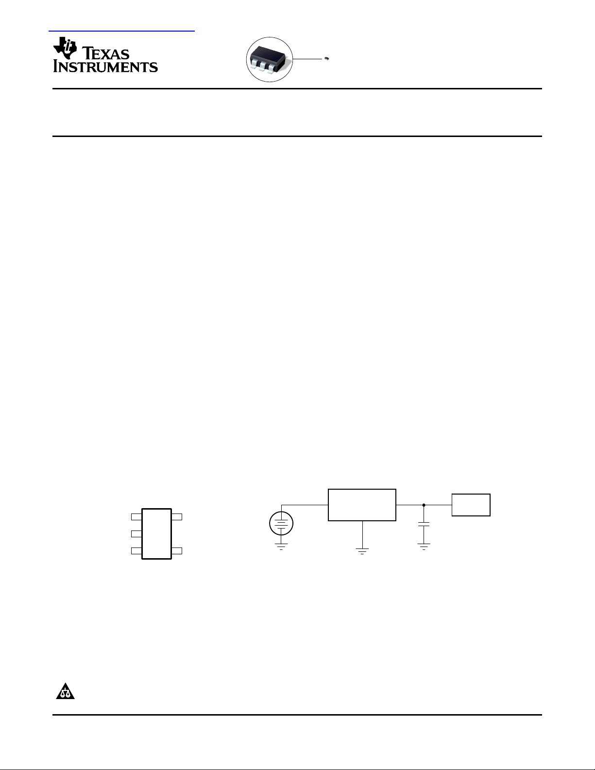
DCK PACKAGE
(TOP VIEW)
1FB/NC
GND
NC
OUT
IN
GND
TPS715xx
OUT
IN
MSP430
Solar
Cell
查询BQ71533DCKRG4供应商
50 mA, 24 V, 3.2 µA Supply Current
Low-Dropout Linear Regulator in SC70 Package
FEATURES APPLICATIONS
• 24-V Maximum Input Voltage
• Low 3.2-µA Quiescent Current at 50 mA
• Stable With Any Capacitor ( ≥ 0.47 µF)
• 50-mA Low-Dropout Regulator
• Available in 1.8 V, 1.9 V, 2.3 V, 2.5 V, 3.0 V, 3.3
V, 3.45 V, 5.0 V, and Adjustable (1.2 V to 15 V)
• Designed to Support MSP430 Families:
– 1.9 V version ensured to be higher than
minimum V
– 2.3 V version ensured to meet 2.2 V
minimum V
– 3.45 V version ensured to be lower than
maximum V
– Wide variety of fixed output voltage options
to match V
desired MSP430 speed
• Minimum/Maximum Specified Current Limit
• 5-Pin SC70/SOT-323 (DCK) Package
• -40°C to +125°C Specified Junction
Temperature Range
• For 80mA Rated Current and Higher Power
Package, see TPS715Axx
of 1.8 V
IN
for FLASH on MSP430F2xx
IN
of 3.6 V
IN
to the minimum required for
IN
TPS715xx
SLVS338K – MAY 2001 – REVISED SEPTEMBER 2005
• Ultra Low Power Microcontrollers
• Cellular/Cordless Handsets
• Portable/Battery-Powered Equipment
DESCRIPTION
The TPS715xx low-dropout (LDO) voltage regulators
offer the benefits of high input voltage, low-dropout
voltage, low-power operation, and miniaturized packaging. The devices, which operate over an input
range of 2.5 V to 24 V, are stable with any capacitor
( ≥ 0.47 µF). The low dropout voltage and low
quiescent current allow operations at extremely low
power levels. Therefore, the devices are ideal for
powering battery management ICs. Specifically, since
the devices are enabled as soon as the applied
voltage reaches the minimum input voltage, the
output is quickly available to power continuously
operating battery charging ICs.
The usual PNP pass transistor has been replaced by
a PMOS pass element. Because the PMOS pass
element behaves as a low-value resistor, the low
dropout voltage, typically 415 mV at 50 mA of load
current, is directly proportional to the load current.
The low quiescent current (3.2 µA typically) is stable
over the entire range of output load current (0 mA to
50 mA).
Please be aware that an important notice concerning availability, standard warranty, and use in critical applications of Texas
Instruments semiconductor products and disclaimers thereto appears at the end of this data sheet.
All trademarks are the property of their respective owners.
PRODUCTION DATA information is current as of publication date.
Products conform to specifications per the terms of the Texas
Instruments standard warranty. Production processing does not
necessarily include testing of all parameters.
Copyright © 2001–2005, Texas Instruments Incorporated
Page 2
www.ti.com
TPS715xx
SLVS338K – MAY 2001 – REVISED SEPTEMBER 2005
This integrated circuit can be damaged by ESD. Texas Instruments recommends that all integrated
circuits be handled with appropriate precautions. Failure to observe proper handling and installation
procedures can cause damage.
ESD damage can range from subtle performance degradation to complete device failure. Precision
integrated circuits may be more susceptible to damage because very small parametric changes could
cause the device not to meet its published specifications.
ORDERING INFORMATION
PRODUCT V
TPS715 xxyyyz XX is nominal output voltage (for example, 28 = 2.8V, 285 = 2.85V, 01 = Adjustable).
YYY is package designator.
Z is package quantity.
(1) For the most current package and ordering information, see the Package Option Addendum at the end of this document, or see the TI
website at www.ti.com .
(2) Output voltages from 1.25V to 5.4V in 50mV increments are available through the use of innovative factory EEPROM programming;
minimum order quantities may apply. Contact factory for details and availability.
(1)
(2)
OUT
ABSOLUTE MAXIMUM RATINGS
over operating temperature range (unless otherwise noted)
VINrange -0.3 V to 24 V
Peak output current Internally limited
ESD rating, HBM 2 kV
ESD rating, CDM 500 V
Continuous total power dissipation See Dissipation Rating Table
Junction temperature range, T
Storage temperature range, T
(1) Stresses beyond those listed under absolute maximum ratings may cause permanent damage to the device. These are stress ratings
only, and functional operation of the device at these or any other conditions beyond those indicated under recommended operating
conditions is not implied. Exposure to absolute-maximum-rated conditions for extended periods may affect device reliability.
(2) All voltage values are with respect to network ground terminal.
J
stg
(1) (2)
UNIT
-40°C to +150°C
-65°C to +150°C
DISSIPATION RATING TABLE
BOARD PACKAGE R
(1)
Low-K
(2)
High-K
(1) The JEDEC Low-K (1s) board design used to derive this data was a 3 inch x 3 inch, two-layer board with 2 ounce copper traces on top
of the board.
(2) The JEDEC High-K (2s2p) board design used to derive this data was a 3 inch x 3 inch, multilayer board with 1 ounce internal power and
ground planes and 2 ounce copper traces on top and bottom of the board.
2
DCK 165 395 2.52 mW/°C 250 mW 140 mW 100 mW
DCK 165 315 3.18 mW/°C 320 mW 175 mW 130 mW
°C/W R
θ JC
°C/W
θ JA
DERATING FACTOR TA≤ 25°C TA= 70°C TA= 85°C
ABOVE TA= 25°C POWER RATING POWER RATING POWER RATING
Page 3
www.ti.com
SLVS338K – MAY 2001 – REVISED SEPTEMBER 2005
ELECTRICAL CHARACTERISTICS
over operating junction temperature range (T
otherwise noted. Typical values are at TJ= 25°C.
PARAMETER TEST CONDITIONS MIN TYP MAX UNIT
Input voltage
V
OUT
V
OUT
Ground pin current I
Load regulation ∆ V
Output voltage
line regulation
Output noise voltage V
Output current limit I
Power-supply ripple rejection PSRR f = 100 kHz, C
Dropout voltage
VIN= V
(1)
V
IN
voltage range (TPS71501) 1.2 15 V
accuracy
(1)
Over VIN, I
OUT
∆ V
OUT
(1)
OUT(NOM)
- 1 V
, and T -4.0 +4.0 %
OUT
GND
/ ∆ I
OUT
/ ∆ V
IN
n
CL
V
DO
= -40°C to 125°C) , V
J
= V
IN
OUT(NOM)
+ 1 V, I
OUT
= 1 mA, C
= 1 µF unless
OUT
IO= 10 mA 2.5 24
IO= 50 mA 3 24
VIN+ 1.0 V ≤ VIN≤ 24 V
100 µA ≤ I
0 ≤ I
OUT
0 mA ≤ I
0 mA ≤ I
I
= 100 µA to 50 mA 22 mV
OUT
V
+ 1 V < VIN≤ 24 V 20 60 mV
OUT
BW = 200 Hz to 100 kHz, C
I
= 50 mA
OUT
≤ 50 mA
OUT
≤ 50 mA, TJ= -40°C to +85°C 3.2 4.2
≤ 50 mA 3.2 4.8 µA
OUT
≤ 50 mA, VIN= 24 V 5.8
OUT
= 10 µF,
OUT
575 µVrms
VO= 0 V 125 750 mA
= 10 µF 60 dB
OUT
I
= 50 mA 415 750 mV
OUT
TPS715xx
V
(1) Minimum VIN= V
+ V
OUT
or the value shown for Input voltage in this table, whichever is greater.
DO
3
Page 4
www.ti.com
_
+
Current
Sense
R1
R2
V
(IN)
GND
V
(OUT)
ILIM
Bandgap
Reference
V
ref
= 1.205 V
FB
_
+
Current
Sense
R1
R2
V
(IN)
GND
V
(OUT)
ILIM
Bandgap
Reference
V
ref
= 1.205 V
R2 = 840 kΩ
TPS715xx
SLVS338K – MAY 2001 – REVISED SEPTEMBER 2005
FUNCTIONAL BLOCK DIAGRAM—ADJUSTABLE VERSION
FUNCTIONAL BLOCK DIAGRAM—FIXED VERSION
Table 1. Terminal Functions
TERMINAL
NAME
FB 1 Adjustable version. This terminal is used to set the output voltage.
NC 1 No connection
GND 2 2 Ground
NC 3 3 No connection
IN 4 4 Input supply.
OUT 5 5 Output of the regulator, any output capacitor ≥ 0.47 µF can be used for stability.
4
FIXED ADJ.
NO. DESCRIPTION
Page 5

www.ti.com
3.290
3.295
3.300
3.305
3.310
3.315
3.320
0 10 20 30 40 50
I
O
− Output Current − mA
VIN = 4.3 V
C
OUT
= 1 µF
TJ = 25°C
V
OUT
− Output Voltage − V
−40−25−10 5 20 35 50 65 80 95 110125
T
J
− Junction Temperature − °C
3.25
3.26
3.27
3.28
3.29
3.30
3.31
3.32
VIN = 4.3 V
C
OUT
= 1 µF
I
OUT
= 50 mA
I
OUT
= 1 mA
V
OUT
− Output Voltage − V
2
2.5
3
3.5
4
4.5
−40−25−10 5 20 35 50 65 80 95 110125
T
J
− Junction Temperature − °C
VIN = 4.3 V
V
OUT
= 3.3 V
I
OUT
= 1 µF
I
GND
− Ground Current − µ A
100 1 k 10 k 100 k
f − Frequency − Hz
I
OUT
= 1 mA
I
OUT
= 50 mA
µ HzOutput Spectral Noise Density −
0
1
2
3
4
5
6
7
8
VIN = 4.3 V
V
OUT
= 3.3 V
C
OUT
= 1 µF
V/
f − Frequency − Hz
− Output Impedance −Z
o
Ω
14
8
0
12
2
4
10
VIN = 4.3 V
V
OUT
= 3.3 V
C
OUT
= 1 µF
TJ = 25°C
I
OUT
= 1 mA
100 1 M10 1k 10k 100k 10 M
I
OUT
= 50 mA
6
16
18
0
100
200
300
400
500
600
0 10 20 30 40 50
TJ = 125°C
TJ = 25°C
TJ = −40°C
VIN = 3.2 V
C
OUT
= 1 µF
I
OUT
− Output Current − mA
− Dropout Voltage − mV
V
DO
0
0.1
0.2
0.4
0.5
0.6
0.7
0.8
0.9
1
0 3 6 9 12 15
V
IN
− Input Voltage − V
− Dropout Voltage − V
V
DO
I
OUT
= 50 mA
TJ = 25°C
TJ = −40°C
TJ = 125°C
0.3
TJ − Junction Temperature − °C
− Dropout Voltage − mV
V
DO
−40 5−25 20 35 65 110 12550−10 80
95
VIN = 3.2 V
I
OUT
= 50 mA
I
OUT
= 10 mA
0
100
200
300
400
500
600
f − Frequency − Hz
0
80
50
10
70
20
30
60
VIN = 4.3 V
V
OUT
= 3.3 V
C
OUT
= 10 µF
TJ = 25°C
I
OUT
= 1 mA
100 1 M10 1k 10k 100k 10 M
I
OUT
= 50 mA
40
90
100
PSRR − Power Supply Ripple Rejection − dB
TPS715xx
SLVS338K – MAY 2001 – REVISED SEPTEMBER 2005
TYPICAL CHARACTERISTICS
OUTPUT VOLTAGE OUTPUT VOLTAGE QUIESCENT CURRENT
vs vs vs
OUTPUT CURRENT JUNCTION TEMPERATURE JUNCTION TEMPERATURE
Figure 1. Figure 2. Figure 3.
OUTPUT SPECTRAL OUTPUT IMPEDANCE DROPOUT VOLTAGE
NOISE DENSITY vs vs
vs FREQUENCY OUTPUT CURRENT
FREQUENCY
DROPOUT VOLTAGE vs RIPPLE REJECTION
INPUT VOLTAGE FREQUENCY
Figure 4. Figure 5. Figure 6.
TPS71501 DROPOUT VOLTAGE POWER-SUPPLY
vs JUNCTION TEMPERATURE vs
Figure 7. Figure 8. Figure 9.
5
Page 6

www.ti.com
t − Time − µs
0 300200100 400 500 700600 800 900 1000
0
400
60
40
20
-200
VIN = 4.3 V
V
OUT
= 3.3 V
C
OUT
= 10 µF
200
0
I
OUT
− Output Current − mV
V
OUT
− Change In
Output Voltage − mV
18161412
V
IN
V
OUT
V
OUT
= 3.3 V
RL = 66 Ω
C
OUT
= 10 µF
8
7
6
5
4
3
2
1
0
t − Time − ms
20 64 108 20
V
OUT
− Output Voltage − V
V
IN
− Input Voltage − V
t − Time − µs
0 15010050 200 250 350300 400 450 500
5.3
V
OUT
= 3.3 V
I
OUT
= 50 mA
C
OUT
= 10 µF
4.3
100
50
0
−50
V
OUT
− Change in
Output Voltage − mV
V
IN
− Input Voltage − V
TPS715xx
SLVS338K – MAY 2001 – REVISED SEPTEMBER 2005
TYPICAL CHARACTERISTICS (continued)
POWER UP / POWER DOWN LINE TRANSIENT RESPONSE LOAD TRANSIENT RESPONSE
Figure 10. Figure 11. Figure 12.
6
Page 7

www.ti.com
TPS71533
IN OUT
V
IN
V
OUT
C1
0.1µF
0.47µF
GND
P
D(max)
TJmax T
A
R
JA
P
D
VINV
OUT
I
OUT
TPS715xx
SLVS338K – MAY 2001 – REVISED SEPTEMBER 2005
APPLICATION INFORMATION
The TPS715xx family of LDO regulators has been optimized for ultra-low power applications such as the
MSP430 microcontroller. Its ultra-low supply current maximizes efficiency at light loads, and its high input voltage
range makes it suitable for supplies such as unconditioned solar panels.
Figure 13. Typical Application Circuit (Fixed Voltage Version)
External Capacitor Requirements
Although not required, a 0.047-µF or larger input bypass capacitor, connected between IN and GND and located
close to the device, is recommended to improve transient response and noise rejection of the power supply as a
whole. A higher-value input capacitor may be necessary if large, fast-rise-time load transients are anticipated and
the device is located several inches from the power source.
The TPS715xx requires an output capacitor connected between OUT and GND to stabilize the internal control
loop. Any capacitor (including ceramic and tantalum) ≥ 0.47 µF properly stabilizes this loop. X7R type capacitors
are recommended but X5R and others may be used.
Power Dissipation and Junction Temperature
To ensure reliable operation, worst-case junction temperature should not exceed 125°C. This restriction limits the
power dissipation the regulator can handle in any given application. To ensure the junction temperature is within
acceptable limits, calculate the maximum allowable dissipation, P
must be less than or equal to P
.
D(max)
, and the actual dissipation, PD, which
D(max)
The maximum-power-dissipation limit is determined using the following equation:
where:
• TJmax is the maximum allowable junction temperature.
• R
is the thermal resistance junction-to-ambient for the package (see the Dissipation Ratings table).
θ JA
• TAis the ambient temperature.
The regulator dissipation is calculated using:
For a higher power package version of the TPS715xx, see the TPS715Axx .
Regulator Protection
The TPS715xx PMOS-pass transistor has a built-in back diode that conducts reverse current when the input
voltage drops below the output voltage (e.g., during power down). Current is conducted from the output to the
input and is not internally limited. If extended reverse voltage operation is anticipated, external limiting might be
appropriate.
The TPS715xx features internal current limiting. During normal operation, the TPS715xx limits output current to
approximately 500 mA. When current limiting engages, the output voltage scales back linearly until the
overcurrent condition ends. Take care not to exceed the power dissipation ratings of the package.
(1)
(2)
7
Page 8

www.ti.com
V
OUT
V
REF
1
R1
R2
R1
V
OUT
V
REF
1 R2
OUTPUT VOLTAGE
PROGRAMMING GUIDE
OUTPUT
VOLTAGE
R1 R2
1.8 V
2.8 V
5.0 V
0.499 MΩ
1.33 MΩ
3.16 MΩ
1 MΩ
1 MΩ
1 MΩ
GND
FB
IN OUT
V
IN
V
OUT
R
1
C
FB
R
2
TPS71501
V
OUT
V
REF
1
R1
R2
0.1µF 0.47µF
TPS715xx
SLVS338K – MAY 2001 – REVISED SEPTEMBER 2005
APPLICATION INFORMATION (continued)
Programming the TPS71501 Adjustable LDO Regulator
The output voltage of the TPS71501 adjustable regulator is programmed using an external resistor divider as
shown in Figure 14 . The output voltage operating range is 1.2 V to 15 V, and is calculated using:
where:
• V
Resistors R1 and R2 should be chosen for approximately 1.5-µA divider current. Lower value resistors can be
used for improved noise performance, but the solution consumes more power. Higher resistor values should be
avoided as leakage current into/out of FB across R1/R2 creates an offset voltage that artificially increases/decreases the feedback voltage and thus erroneously decreases/increases V
design procedure is to choose R2 = 1 M Ω to set the divider current at 1.5 µA, and then calculate R1 using:
= 1.205 V typ (the internal reference voltage)
REF
. The recommended
OUT
(3)
(4)
Figure 14. TPS71501 Adjustable LDO Regulator Programming
Power the MSP430 Microcontroller
Several versions of the TPS715xx are ideal for powering the MSP430 microcontroller. Table 2 shows potential
applications of some voltage versions.
DEVICE V
TPS71519 1.9V V
TPS71523 2.3V V
TPS71530 3.0V V
TPS715345 2.45V V
The TPS715xx family offers many output voltage versions to allow designers to minimize the supply voltage for
the processing speed required of the MSP430. This minimizes the supply current consumed by the MSP430.
8
(TYP) APPLICATION
OUT
Table 2. Typical MSP430 Applications
> 1.800V required by many MSP430s. Allows lowest power consumption operation.
OUT, MIN
> 2.200V required by some MSP430s FLASH operation.
OUT, MIN
> 2.700V required by some MSP430s FLASH operation.
OUT, MIN
< 3.600V required by some MSP430s. Allows highest speed operation.
OUT, MIN
Page 9

PACKAGE OPTION ADDENDUM
www.ti.com
24-Aug-2005
PACKAGING INFORMATION
Orderable Device Status
(1)
Package
Type
Package
Drawing
Pins Package
Qty
Eco Plan
BQ71525DCKR ACTIVE SC70 DCK 5 3000 Green (RoHS &
no Sb/Br)
BQ71533DCKR ACTIVE SC70 DCK 5 3000 Green (RoHS &
no Sb/Br)
BQ71533DCKRG4 ACTIVE SC70 DCK 5 3000 Green (RoHS &
no Sb/Br)
TPS71501DCKR ACTIVE SC70 DCK 5 3000 Green (RoHS &
no Sb/Br)
TPS71501DCKRG4 ACTIVE SC70 DCK 5 3000 Green (RoHS &
no Sb/Br)
TPS71518DCKR PREVIEW SC70 DCK 5 3000 TBD Call TI Call TI
TPS71519DCKR PREVIEW SC70 DCK 5 3000 TBD Call TI Call TI
TPS71523DCKR PREVIEW SC70 DCK 5 3000 TBD Call TI Call TI
TPS71525DCKR ACTIVE SC70 DCK 5 3000 Green (RoHS &
no Sb/Br)
TPS71525DCKRG4 ACTIVE SC70 DCK 5 3000 Green (RoHS &
no Sb/Br)
TPS71530DCKR ACTIVE SC70 DCK 5 3000 Green (RoHS &
no Sb/Br)
TPS71530DCKRG4 ACTIVE SC70 DCK 5 3000 Green (RoHS &
no Sb/Br)
TPS71530QDCKRQ1 ACTIVE SC70 DCK 5 3000 TBD CU NIPDAU Level-1-260C-UNLIM
TPS71533DCKR ACTIVE SC70 DCK 5 3000 Green (RoHS &
no Sb/Br)
TPS71533DCKRG4 ACTIVE SC70 DCK 5 3000 Green (RoHS &
no Sb/Br)
TPS715345DCKR PREVIEW SC70 DCK 5 3000 TBD Call TI Call TI
TPS71550DCKR ACTIVE SC70 DCK 5 3000 Green (RoHS &
no Sb/Br)
TPS71550DCKRG4 ACTIVE SC70 DCK 5 3000 Green (RoHS &
no Sb/Br)
(1)
The marketing status values are defined as follows:
ACTIVE: Product device recommended for new designs.
LIFEBUY: TI has announced that the device will be discontinued, and a lifetime-buy period is in effect.
NRND: Not recommended for new designs. Device is in production to support existing customers, but TI does not recommend using this part in
a new design.
PREVIEW: Device has been announced but is not in production. Samples may or may not be available.
OBSOLETE: TI has discontinued the production of the device.
(2)
Lead/Ball Finish MSL Peak Temp
CU NIPDAU Level-1-260C-UNLIM
CU NIPDAU Level-1-260C-UNLIM
CU NIPDAU Level-1-260C-UNLIM
CU NIPDAU Level-1-260C-UNLIM
CU NIPDAU Level-1-260C-UNLIM
CU NIPDAU Level-1-260C-UNLIM
CU NIPDAU Level-1-260C-UNLIM
CU NIPDAU Level-1-260C-UNLIM
CU NIPDAU Level-1-260C-UNLIM
CU NIPDAU Level-1-260C-UNLIM
CU NIPDAU Level-1-260C-UNLIM
CU NIPDAU Level-1-260C-UNLIM
CU NIPDAU Level-1-260C-UNLIM
(3)
(2)
Eco Plan - The planned eco-friendly classification: Pb-Free (RoHS) or Green (RoHS & no Sb/Br) - please check
http://www.ti.com/productcontent for the latest availability information and additional product content details.
TBD: The Pb-Free/Green conversion plan has not been defined.
Pb-Free (RoHS): TI's terms "Lead-Free" or "Pb-Free" mean semiconductor products that are compatible with the current RoHS requirements
for all 6 substances, including the requirement that lead not exceed 0.1% by weight in homogeneous materials. Where designed to be soldered
at high temperatures, TI Pb-Free products are suitable for use in specified lead-free processes.
Green (RoHS & no Sb/Br): TI defines "Green" to mean Pb-Free (RoHS compatible), and free of Bromine (Br) and Antimony (Sb) based flame
retardants (Br or Sb do not exceed 0.1% by weight in homogeneous material)
(3)
MSL, Peak Temp. -- The Moisture Sensitivity Level rating according to the JEDEC industry standard classifications, and peak solder
temperature.
Addendum-Page 1
Page 10

PACKAGE OPTION ADDENDUM
www.ti.com
Important Information and Disclaimer:The information provided on this page represents TI's knowledge and belief as of the date that it is
provided. TI bases its knowledge and belief on information provided by third parties, and makes no representation or warranty as to the
accuracy of such information. Efforts are underway to better integrate information from third parties. TI has taken and continues to take
reasonable steps to provide representative and accurate information but may not have conducted destructive testing or chemical analysis on
incoming materials and chemicals. TI and TI suppliers consider certain information to be proprietary, and thus CAS numbers and other limited
information may not be available for release.
In no event shall TI's liability arising out of such information exceed the total purchase price of the TI part(s) at issue in this document sold by TI
to Customer on an annual basis.
24-Aug-2005
Addendum-Page 2
Page 11

MECHANICAL DATA
MPDS025C – FEBRUARY 1997 – REVISED FEBRUARY 2002
DCK (R-PDSO-G5) PLASTIC SMALL-OUTLINE P ACKAGE
0,65
1 3
1,10
0,80
2,15
1,85
45
0,10
0,00
0,30
0,15
1,40
1,10
0,10
2,40
1,80
Seating Plane
M
0,13 NOM
Gage Plane
0,15
0°–8°
0,10
0,46
0,26
NOTES: A. All linear dimensions are in millimeters.
B. This drawing is subject to change without notice.
C. Body dimensions do not include mold flash or protrusion.
D. Falls within JEDEC MO-203
4093553-2/D 01/02
POST OFFICE BOX 655303 • DALLAS, TEXAS 75265
Page 12

IMPORTANT NOTICE
Texas Instruments Incorporated and its subsidiaries (TI) reserve the right to make corrections, modifications,
enhancements, improvements, and other changes to its products and services at any time and to discontinue
any product or service without notice. Customers should obtain the latest relevant information before placing
orders and should verify that such information is current and complete. All products are sold subject to TI’s terms
and conditions of sale supplied at the time of order acknowledgment.
TI warrants performance of its hardware products to the specifications applicable at the time of sale in
accordance with TI’s standard warranty. Testing and other quality control techniques are used to the extent TI
deems necessary to support this warranty . Except where mandated by government requirements, testing of all
parameters of each product is not necessarily performed.
TI assumes no liability for applications assistance or customer product design. Customers are responsible for
their products and applications using TI components. To minimize the risks associated with customer products
and applications, customers should provide adequate design and operating safeguards.
TI does not warrant or represent that any license, either express or implied, is granted under any TI patent right,
copyright, mask work right, or other TI intellectual property right relating to any combination, machine, or process
in which TI products or services are used. Information published by TI regarding third-party products or services
does not constitute a license from TI to use such products or services or a warranty or endorsement thereof.
Use of such information may require a license from a third party under the patents or other intellectual property
of the third party, or a license from TI under the patents or other intellectual property of TI.
Reproduction of information in TI data books or data sheets is permissible only if reproduction is without
alteration and is accompanied by all associated warranties, conditions, limitations, and notices. Reproduction
of this information with alteration is an unfair and deceptive business practice. TI is not responsible or liable for
such altered documentation.
Resale of TI products or services with statements different from or beyond the parameters stated by TI for that
product or service voids all express and any implied warranties for the associated TI product or service and
is an unfair and deceptive business practice. TI is not responsible or liable for any such statements.
Following are URLs where you can obtain information on other Texas Instruments products and application
solutions:
Products Applications
Amplifiers amplifier.ti.com Audio www.ti.com/audio
Data Converters dataconverter.ti.com Automotive www.ti.com/automotive
DSP dsp.ti.com Broadband www.ti.com/broadband
Interface interface.ti.com Digital Control www.ti.com/digitalcontrol
Logic logic.ti.com Military www.ti.com/military
Power Mgmt power.ti.com Optical Networking www.ti.com/opticalnetwork
Microcontrollers microcontroller.ti.com Security www.ti.com/security
Telephony www.ti.com/telephony
Video & Imaging www.ti.com/video
Wireless www.ti.com/wireless
Mailing Address: Texas Instruments
Post Office Box 655303 Dallas, Texas 75265
Copyright 2005, Texas Instruments Incorporated
 Loading...