

1
2
3
4
5
6
7
8
9
10
20
19
18
17
16
15
14
13
12
11
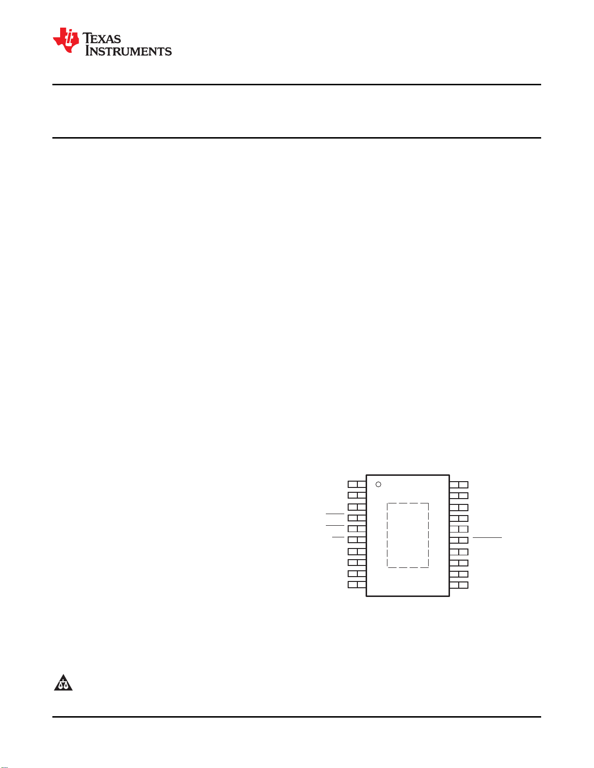
PWP PACKAGE
(TOP VIEW)
NC
V
IN1
V
IN1
MR1
MR2
EN
SEQ
GND
V
IN2
V
IN2
NC
V
OUT1
V
OUT1
V
SENSE1
/FB1
PG1
RESET
V
SENSE2
/FB2
V
OUT2
V
OUT2
NC
www.ti.com
TPS70145, TPS70148
TPS70151, TPS70158
TPS70102
SLVS222I –DECEMBER 1999–REVISED AUGUST 2010
Dual-Output Low Dropout Voltage Regulators
with Power-Up Sequencing for Split-Voltage DSP Systems
Check for Samples: TPS70145, TPS70148, TPS70151, TPS70158, TPS70102
1
FEATURES
23
• Dual Output Voltages for Split-Supply
Applications
• Selectable Power-Up Sequencing for DSP
Applications
• Output Current Range of 500mA on Regulator
1 and 250mA on Regulator 2
• Fast Transient Response
• Voltage Options: 3.3V/2.5V, 3.3V/1.8V,
3.3V/1.5V, 3.3V/1.2V, and Dual Adjustable
Outputs
• Open Drain Power-On Reset with 120ms Delay
• Open Drain Power Good for Regulator 1
• Ultra Low 190mA (typ) Quiescent Current
• 1mA Input Current During Standby
• Low Noise: 65mV
Without Bypass Capacitor
RMS
• Quick Output Capacitor Discharge Feature
• Two Manual Reset Inputs
• 2% Accuracy Over Load and Temperature
• Undervoltage Lockout (UVLO) Feature
• 20-Pin PowerPAD™ TSSOP Package
• Thermal Shutdown Protection
DESCRIPTION
TPS701xx family devices are designed to provide a
complete power management solution for the
TMS320™ DSP family, processor power, ASIC,
FPGA, and digital applications where dual output
voltage regulators are required. Easy programmability
of the sequencing function makes the TPS701xx
family ideal for any TMS320 DSP applications with
power sequencing requirements. Differentiated
features, such as accuracy, fast transient response,
SVS supervisory circuit, manual reset inputs, and an
enable function, provide a complete system solution.
The TPS701xx family of voltage regulators offer very
low dropout voltage and dual outputs with power-up
sequence control, which is designed primarily for
DSP applications. These devices have extremely low
noise output performance without using any added
filter bypass capacitors and are designed to have a
fast transient response and be stable with 10mF low
ESR capacitors.
These devices have fixed 3.3V/2.5V, 3.3V/1.8V,
3.3V/1.5V, 3.3V/1.2V, and adjustable/adjustable
voltage options. Regulator 1 can support up to
500mA, and regulator 2 can support up to 250mA.
Separate voltage inputs allow the designer to
configure the source power.
1
2PowerPAD, TMS320 are trademarks of Texas Instruments.
3All other trademarks are the property of their respective owners.
PRODUCTION DATA information is current as of publication date.
Products conform to specifications per the terms of the Texas
Instruments standard warranty. Production processing does not
necessarily include testing of all parameters.
Please be aware that an important notice concerning availability, standard warranty, and use in critical applications of Texas
Instruments semiconductor products and disclaimers thereto appears at the end of this data sheet.
Copyright © 1999–2010, Texas Instruments Incorporated
1.8 V
V
IN1
V
IN2
EN
SEQ
V
OUT1
V
SENSE1
PG1
MR2
RESET
MR1
V
SENSE2
V
OUT2
TPS70151 PWP
5 V
3.3 V
I/O
MR1
Core
0.1 µF
RESET
10 µF
10 µF
0.1 µF
DSP
MR2
PG1
EN
250 kΩ
>2 V
<0.7 V
250 kΩ
>2 V
<0.7 V
>2 V
<0.7 V
TPS70145, TPS70148
TPS70151, TPS70158
TPS70102
SLVS222I –DECEMBER 1999–REVISED AUGUST 2010
www.ti.com
Because the PMOS device behaves as a low-value resistor, the dropout voltage is very low (typically 170mV on
regulator 1) and is directly proportional to the output current. Additionally, since the PMOS pass element is a
voltage-driven device, the quiescent current is very low and independent of output loading (maximum of 230mA
over the full range of output current). This LDO family also features a sleep mode; applying a high signal to EN
(enable) shuts down both regulators, reducing the input current to 1mA at TJ= +25°C.
The device is enabled when the EN pin is connected to a low-level input voltage. The output voltages of the two
regulators are sensed at the V
SENSE1
and V
SENSE2
pins, respectively.
The input signal at the SEQ pin controls the power-up sequence of the two regulators. When the device is
enabled and the SEQ terminal is pulled high or left open, V
reaches approximately 83% of its regulated output voltage. At that time V
below 83% (for example, an overload condition), V
power-up order and V
is turned on first. The SEQ pin is connected to an internal pull-up current source.
OUT1
is turned off. Pulling the SEQ terminal low reverses the
OUT1
turns on first and V
OUT2
OUT1
is turned on. If V
OUT1
remains off until V
is pulled
OUT2
OUT2
For each regulator, there is an internal discharge transistor to discharge the output capacitor when the regulator
is turned off (disabled).
The PG1 pin reports the voltage conditions at V
, which can be used to implement an SVS for the circuitry
OUT1
supplied by regulator 1.
The TPS701xx features a RESET (SVS, POR, or Power-On Reset). RESET output initiates a reset in DSP
systems and related digital applications in the event of an undervoltage condition. RESET indicates the status of
V
and both manual reset pins (MR1 and MR2). When V
OUT2
and MR2 are in the logic high state, RESET goes to a high impedance state after a 120ms delay. RESET goes
to the logic low state when the V
condition) of its regulated voltage. To monitor V
The device has an undervoltage lockout (UVLO) circuit that prevents the internal regulators from turning on until
V
reaches 2.5V.
IN1
regulated output voltage is pulled below 95% (for example, an overload
OUT2
OUT1
, the PG1 output pin can be connected to MR1 or MR2.
reaches 95% of its regulated voltage and MR1
OUT2
2 Submit Documentation Feedback Copyright © 1999–2010, Texas Instruments Incorporated
www.ti.com
TPS70145, TPS70148
TPS70151, TPS70158
TPS70102
SLVS222I –DECEMBER 1999–REVISED AUGUST 2010
This integrated circuit can be damaged by ESD. Texas Instruments recommends that all integrated circuits be handled with
appropriate precautions. Failure to observe proper handling and installation procedures can cause damage.
ESD damage can range from subtle performance degradation to complete device failure. Precision integrated circuits may be more
susceptible to damage because very small parametric changes could cause the device not to meet its published specifications.
(1)
VOLTAGE (V)
ORDERING INFORMATION
(2)
PACKAGE- SPECIFIED
LEAD TEMPERATURE ORDERING TRANSPORT
PRODUCT V
OUT1
TPS70102 Adjustable Adjustable HTSSOP-20 (PWP) -40°C to +125°C
TPS70145 3.3 V 1.2 V HTSSOP-20 (PWP) -40°C to +125°C
TPS70148 3.3 V 1.5 V HTSSOP-20 (PWP) -40°C to +125°C
TPS70151 3.3 V 1.8 V HTSSOP-20 (PWP) -40°C to +125°C
TPS70158 3.3 V 2.5 V HTSSOP-20 (PWP) -40°C to +125°C
V
OUT2
(DESIGNATOR) RANGE (TJ) NUMBER MEDIA, QUANTITY
TPS70102PWP Tube, 70
TPS70102PWPR Tape and Reel, 2000
TPS70145PWP Tube, 70
TPS70145PWPR Tape and Reel, 2000
TPS70148PWP Tube, 70
TPS70148PWPR Tape and Reel, 2000
TPS70151PWP Tube, 70
TPS70151PWPR Tape and Reel, 2000
TPS70158PWP Tube, 70
TPS70158PWPR Tape and Reel, 2000
(1) For the most current package and ordering information see the Package Option Addendum located at the end of this document, or see
the TI web site at www.ti.com.
(2) For fixed 1.20V operation, tie FB to OUT.
ABSOLUTE MAXIMUM RATINGS
(1)
Over operating free-air temperature range (unless otherwise noted).
TPS701xx UNIT
Input voltage range: V
IN1
Voltage range at EN –0.3 to +7 V
Output voltage range (V
Output voltage range (V
Maximum RESET, PG1 voltage 7 V
Maximum MR1, MR2, and SEQ voltage V
Peak output current Internally limited —
Continuous total power dissipation See Thermal Information Table —
Junction temperature range, T
Storage temperature range, T
ESD rating, HBM 2 kV
(1) Stresses beyond those listed under absolute maximum ratings may cause permanent damage to the device. These are stress ratings
only, and functional operation of the device at these or any other conditions beyond those indicated under recommended operating
conditions is not implied. Exposure to absolute-maximum-rated conditions for extended periods may affect device reliability.
(2) All voltages are tied to network ground.
, V
OUT1
OUT2
IN2
, V
, V
stg
(2)
) 5.5 V
SENSE1
) 5.5 V
SENSE2
J
–0.3 to +7 V
IN1
–40 to +150 °C
–65 to +150 °C
V
Copyright © 1999–2010, Texas Instruments Incorporated Submit Documentation Feedback 3
LineReg. (mV) + (%ń V) V
O
ǒ
V
Imax
*2.7V
Ǔ
100
1000
LineReg. (mV) + (%ń V) V
O
ǒ
V
Imax
*
ǒ
VO)1V
ǓǓ
100
1000
TPS70145, TPS70148
TPS70151, TPS70158
TPS70102
SLVS222I –DECEMBER 1999–REVISED AUGUST 2010
THERMAL INFORMATION
(1) (2)
q
q
q
y
y
q
JA
JCtop
JB
JT
JB
JCbot
THERMAL METRIC
Junction-to-ambient thermal resistance 74.1
Junction-to-case (top) thermal resistance 43.1
Junction-to-board thermal resistance 19.7
Junction-to-top characterization parameter 2.9
Junction-to-board characterization parameter 17.3
Junction-to-case (bottom) thermal resistance 1.4
(1) For more information about traditional and new thermal metrics, see the IC Package Thermal Metrics application report, SPRA953.
(2) For thermal estimates of this device based on PCB copper area, see the TI PCB Thermal Calculator.
TPS701xx
PWP (20 PINS)
RECOMMENDED OPERATING CONDITIONS
Over operating temperature range (unless otherwise noted)
MIN MAX UNIT
Input voltage, V
Output current, IO(regulator 1) 0 500 mA
Output current, IO(regulator 2) 0 250 mA
Output voltage range (for adjustable option) 1.22 5.5 V
Operating junction temperature, T
(1) To calculate the minimum input voltage for maximum output current, use the following equation: V
(1)
(regulator 1 and 2) 2.7 6 V
I
J
–40 +125 °C
I(min)
= V
O(max)
+ V
DO(max load)
www.ti.com
UNITS
°C/W
.
ELECTRICAL CHARACTERISTICS
Over recommended operating junction temperature range (TJ= –40°C to +125°C), V
EN = 0V, CO= 33mF, (unless otherwise noted).
PARAMETER TEST CONDITIONS MIN TYP MAX UNIT
Reference 2.7V < VI< 6V,
voltage TJ= +25°C
1.2V Output 2.7V < VI< 6V, TJ= +25°C 1.2
V
O
voltage
(2)
Output
1.5V Output 2.7V < VI< 6V, TJ= +25°C 1.5
(1) ,
1.8V Output 2.7V < VI< 6V, TJ= +25°C 1.8
2.5V Output 2.7V < VI< 6V, TJ= +25°C 2.5
3.3V Output 2.7V < VI< 6V, TJ= +25°C 3.3
Quiescent current (GND current) for
regulator 1 and regulator 2, EN = 0V
Output voltage line regulation (∆VO/VO)
for regulator 1 and regulator 2
Load regulation for V
OUT 1
and V
(3)
OUT2
2.7V < VI< 6V, FB connected to V
2.7V < VI< 6V, 1.176 1.224
2.7V < VI< 6V, 1.47 1.53
2.7V < VI< 6V, 1.764 1.836
2.7V < VI< 6V, 2.45 2.55
2.7V < VI< 6V, 3.234 3.366
(2)
(1)
(2)
VO+ 1V < VI≤ 6V, TJ= +25°C
VO+ 1V < VI≤ 6V
TJ= +25°C
FB connected to V
O
O
TJ= +25°C 190
(1)
(1)
(2)
or V
IN2
= V
OUT(nom)
IN1
1.196 1.244
+ 1V, IO= 1mA,
1.22
0.01%
0.1%
1 mV
230
V
mA
V
(1) Minimum input operating voltage is 2.7V or V
current = 1mA.
(2) IO= 1mA to 250mA for Regulator 1 and 1mA to 125mA for Regulator 2.
(3) If VO< 1.8V then V
If VO> 2.5V then V
4 Submit Documentation Feedback Copyright © 1999–2010, Texas Instruments Incorporated
+ 1V, whichever is greater. Maximum input voltage = 6V, minimum output
O(typ)
= 6V, V
Imax
= 6V, V
Imax
Imin
Imin
= 2.7V:
= VO+ 1V:
TPS70145, TPS70148
TPS70151, TPS70158
TPS70102
www.ti.com
ELECTRICAL CHARACTERISTICS (continued)
Over recommended operating junction temperature range (TJ= –40°C to +125°C), V
EN = 0V, CO= 33mF, (unless otherwise noted).
PARAMETER TEST CONDITIONS MIN TYP MAX UNIT
V
n
Output noise
voltage
Output current limit V
Thermal shutdown junction temperature +150 °C
I
I
(standby) current
PSRR 60
Standby
Power-supply ripple f = 1kHz, CO= 33mF, TJ= +25°C
rejection
RESET Terminal
Minimum input voltage for valid RESET I
Trip threshold voltage VOdecreasing 92% 95% 98% V
Hysteresis voltage Measured at V
t
(RESET)
t
r (RESET)
Output low voltage VI= 3.5V, I
Leakage current V
PG1 Terminal
Minimum input voltage for valid PG1 I
Trip threshold voltage VOdecreasing 92% 95% 98% V
Hysteresis voltage Measured at V
t
r(PG1)
Output low voltage VI= 2.7V, I
Leakage current V
EN Terminal
High level EN input voltage 2 V
Low level EN input voltage 0.7 V
Input current (EN) –1 1 mA
Falling edge deglitch Measured at V
SEQ Terminal
High level SEQ input voltage 2 V
Low level SEQ input voltage 0.7 V
SEQ pull-up current source 6 mA
MR1 / MR2 Terminals
High level input voltage 2 V
Low level input voltage 0.7 V
Pull-up current source 6 mA
V
Terminal
OUT2
V
UV comparator: Positive-going
OUT2
input threshold voltage of V
comparator
V
UV comparator: Hysteresis 0.5% V
OUT2
V
UV comparator: Falling edge
OUT2
deglitch
Peak output current 2ms pulse width 375 mA
Regulator 1 65
Regulator 2 65
Regulator 1 1.6 1.9
Regulator 2 0.750 1
Regulator 1 mA
Regulator 2 mA
BW 300Hz to 50kHz, CO= 33mF, TJ= +25°C mV
= 0V A
OUT
EN = VI, TJ= +25°C 1
EN = V
I
EN = VI, TJ= +25°C 1
EN = V
I
= 300mA, V
RESET
O
≤ 0.8V 1.0 1.3 V
(RESET)
RESET pulse duration 80 120 160 ms
Rising edge deglitch 30 ms
O(RESET)
= 6V 1 mA
(RESET)
= 300mA, V
(PG1)
O
= 1mA 0.15 0.4 V
≤ 0.8V 1.0 1.3 V
(PG1)
Rising edge deglitch 30 ms
= 1mA 0.15 0.4 V
O(PG1)
= 6V 1 mA
(PG1)
O
UV 80% VO83% VO86% V
OUT2
V
SENSE_2
decreasing below threshold 140 ms
SLVS222I –DECEMBER 1999–REVISED AUGUST 2010
or V
IN2
= V
OUT(nom)
IN1
(1)
+ 1V, IO= 1mA,
0.5% V
0.5% V
140 ms
O
3
3
O
RMS
dB
OUT
OUT
OUT
OUT
V
mV
Copyright © 1999–2010, Texas Instruments Incorporated Submit Documentation Feedback 5
TPS70145, TPS70148
TPS70151, TPS70158
TPS70102
SLVS222I –DECEMBER 1999–REVISED AUGUST 2010
ELECTRICAL CHARACTERISTICS (continued)
Over recommended operating junction temperature range (TJ= –40°C to +125°C), V
EN = 0V, CO= 33mF, (unless otherwise noted).
PARAMETER TEST CONDITIONS MIN TYP MAX UNIT
Discharge transistor current V
V
Terminal
OUT1
V
UV comparator: Positive-going
OUT1
input threshold voltage of V
comparator
V
UV comparator: Hysteresis 0.5% V
OUT1
V
UV comparator: Falling edge
OUT1
deglitch
V
Terminal, continued
OUT1
Dropout voltage
Dropout voltage
Peak output current
(4)
(4)
(4)
UV 80% VO83% VO86% V
OUT1
Discharge transistor current V
V
UVLO threshold 2.4 2.65 V
IN1
FB Terminal
Input current: TPS70102 FB = 1.8V 1 mA
(4) Input voltage (V
The 3.3V regulator input is set to 3.2V to perform this test.
IN1
or V
IN2
) = V
O(typ)
= 1.5V 7.5 mA
OUT2
V
SENSE_1
IO= 500mA, TJ= +25°C V
IO= 500mA, V
decreasing below threshold 140 ms
= 3.2V 170 mV
IN1
= 3.2V 275 mV
IN1
2ms pulse width 750 mA
= 1.5V 7.5 mA
OUT1
– 100mV. For 1.5V, 1.8V and 2.5V regulators, the dropout voltage is limited by input voltage range.
IN1
or V
IN2
= V
OUT(nom)
+ 1V, IO= 1mA,
O
www.ti.com
O
V
mV
6 Submit Documentation Feedback Copyright © 1999–2010, Texas Instruments Incorporated
UVLO1
Comp
+
-
+
-
+
-
+
-
Thermal
Shutdown
2.5V
+-
Current
Sense
Reference
V
ref
V
ref
ENA_1
FB1
ENA_1
120ms
Delay
0.95xV
ref
FB2
Current
Sense
+-
ENA_2
ENA_2
V
ref
V
IN1
(2Pins)
GND
EN
V
IN2
(2Pins)
SEQ
(seeNoteB)
PG1
MR2
RESET
V
IN1
MR1
V
IN1
RisingEdge
Deglitch
Reset
Comp
V
OUT2
(2Pins)
FallingEdge
Deglitch
0.83 x V
ref
FB2
V UVComp
OUT2
FallingEdge
Deglitch
0.83 x V
ref
FB1
V UVComp
OUT1
Power
Sequence
Logic
ENA_1
ENA_2
V
IN1
10kW
V
SENSE1
(seeNoteA)
V (2Pins)
OUT1
V
SENSE2
(seeNoteA)
10kW
0.95xV
ref
FB1
RisingEdge
Deglitch
PG
Comp
+
-
www.ti.com
TPS70145, TPS70148
TPS70151, TPS70158
TPS70102
SLVS222I –DECEMBER 1999–REVISED AUGUST 2010
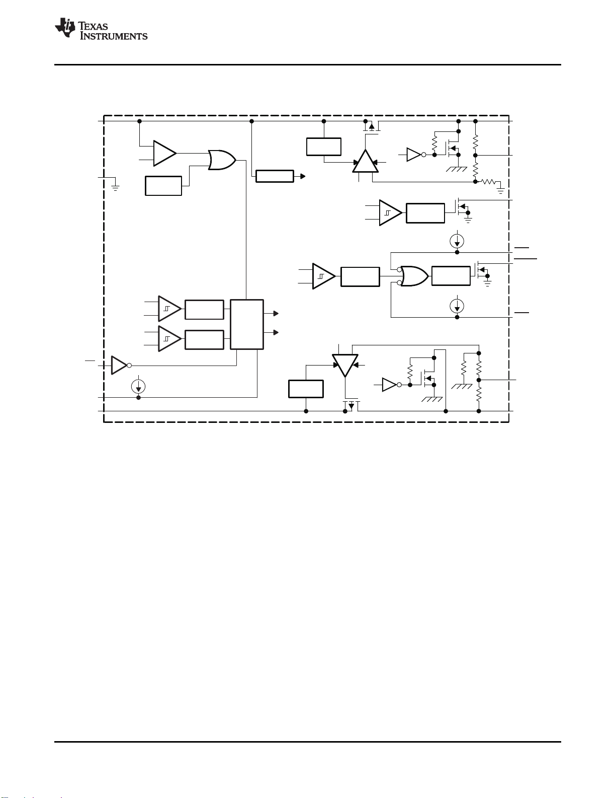
DEVICE INFORMATION
Fixed Voltage Version
A. For most applications, V
SENSE1
and V
should be externally connected to V
SENSE2
as close as possible to the
OUT
device. For other implementations, refer to SENSE terminal connection discussion in the Application Information
section.
B. If the SEQ terminal is floating at the input, V
Copyright © 1999–2010, Texas Instruments Incorporated Submit Documentation Feedback 7
powers up first.
OUT2
UVLO
Comp
+
-
+
-
+
-
+
-
Thermal
Shutdown
2.5V
+-
Current
Sense
Reference
V
ref
V
ref
ENA_1
ENA_1
120ms
Delay
0.95xV
ref
FB1
0.95xV
ref
FB2
RisingEdge
Deglitch
Current
Sense
+-
ENA_2
ENA_2
V
ref
V
IN1
(2Pins)
GND
EN
V
IN2
(2Pins)
SEQ
(seeNoteB)
FB1
(seeNoteA)
PG1
MR2
RESET
FB2
(seeNoteA)
V
IN1
MR1
V
IN1
PG
Comp
RisingEdge
Deglitch
Reset
Comp
V
OUT1
(2Pins)
V
OUT2
(2Pins)
+
-
FallingEdge
Deglitch
0.83 x V
ref
FB2
V UVComp
OUT2
FallingEdge
Deglitch
0.83 x V
ref
FB1
V UVComp
OUT1
Power
Sequence
Logic
ENA_1
ENA_2
V
IN1
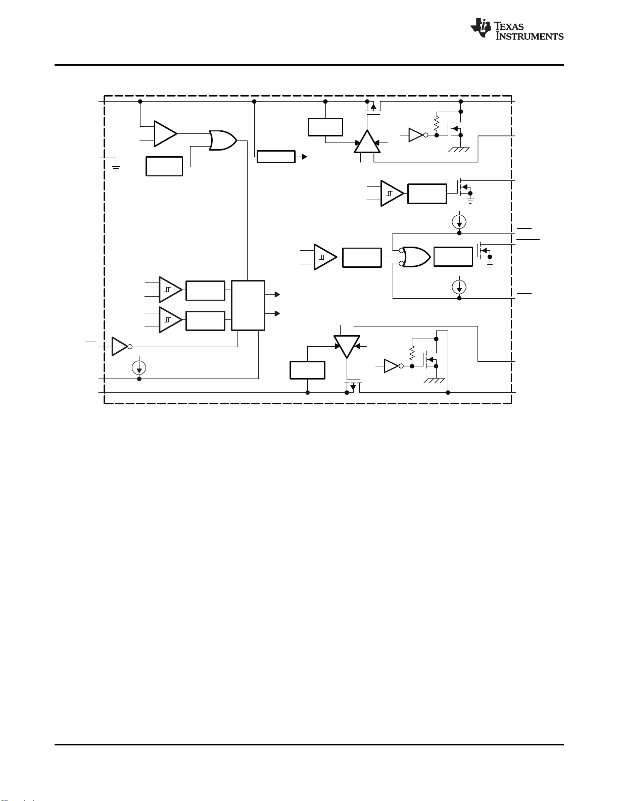
TPS70145, TPS70148
TPS70151, TPS70158
TPS70102
SLVS222I –DECEMBER 1999–REVISED AUGUST 2010
www.ti.com
Adjustable Voltage Version
A. For most applications, FB1 and FB2 should be externally connected to resistor dividers as close as possible to the
device. For other implementations, refer to FB terminals connection discussion in the Application Information
section.
B. If the SEQ terminal is floating at the input, V
8 Submit Documentation Feedback Copyright © 1999–2010, Texas Instruments Incorporated
powers up first
OUT2
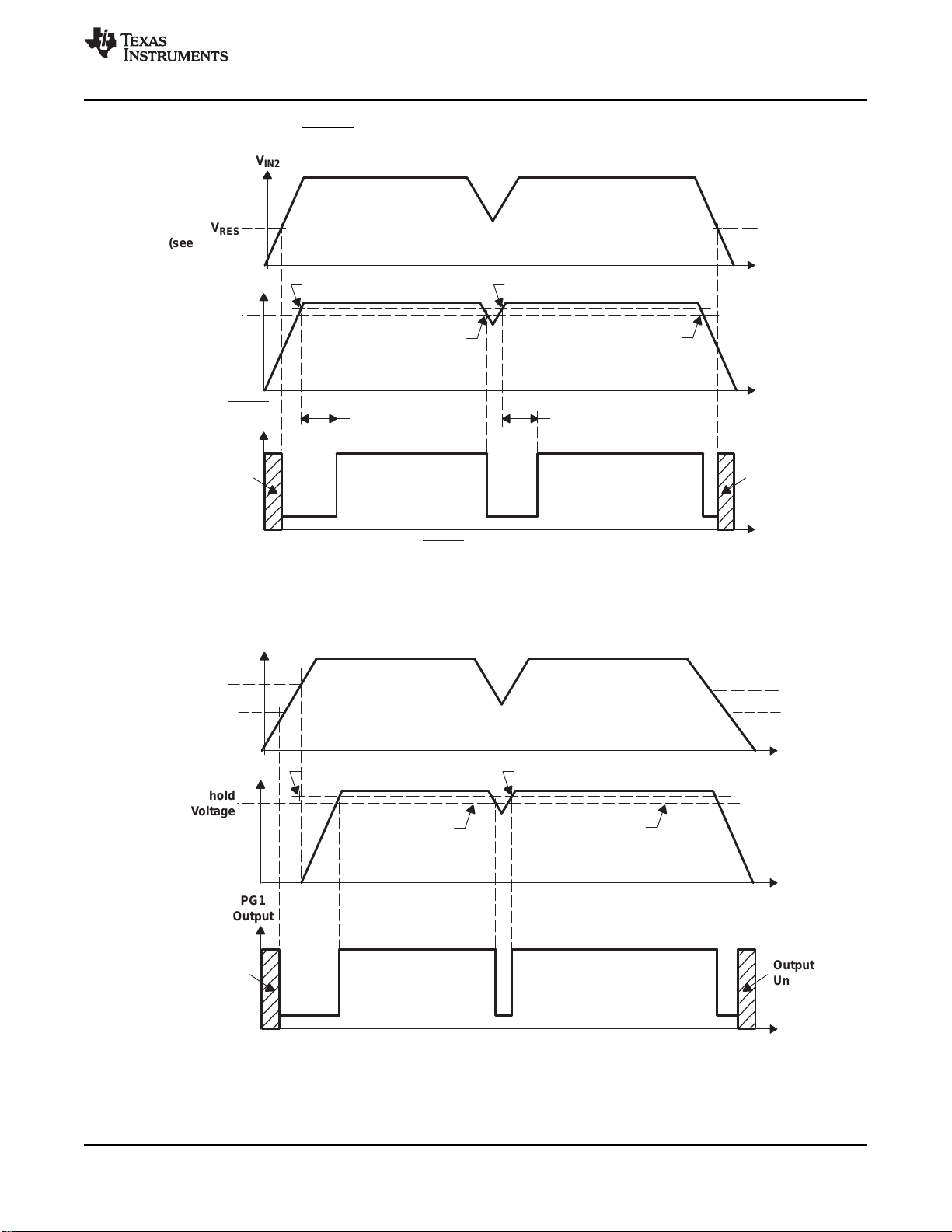
NOTES: A. V
RES
is the minimum input voltage for a valid RESET. The symbol V
RES
is not currently listed within EIA or JEDEC standards
for semiconductor symbology .
Î
Î
Î
Î
Î
V
IN2
V
RES
(see Note A)
V
RES
t
t
t
V
OUT2
Threshold
Voltage
RESET
Output
120 ms
Delay
120 ms
Delay
Output
Undefined
Output
Undefined
V
IT+
(see Note B)
V
IT−
(see Note B)
V
IT+
(see Note B)
B. VIT −Trip voltage is typically 5% lower than the output voltage (95%VO) V
IT−
to V
IT+
is the hysteresis voltage.
V
IT−
(see Note B)
NOTES: A. V
PG1
is the minimum input voltage for a valid PG1. The symbol V
PG1
is not currently listed within EIA or JEDEC
standards for semiconductor symbology.
V
PG1
t
t
t
Threshold
Voltage
PG1
Output
Output
Undefined
Output
Undefined
V
IT+
(see Note B)V
IT+
(see Note B)
B. VIT −Trip voltage is typically 5% lower than the output voltage (95%VO) V
IT−
to V
IT+
is the hysteresis voltage.
V
IN1
V
OUT2
V
PG1
(see Note A)
V
IT−
(see Note B)
V
IT−
(see Note B)
V
UVLO
V
UVLO
www.ti.com
TPS70145, TPS70148
TPS70151, TPS70158
TPS70102
SLVS222I –DECEMBER 1999–REVISED AUGUST 2010
RESET Timing Diagram (with V
Powered Up)
IN1
PG1 Timing Diagram
Copyright © 1999–2010, Texas Instruments Incorporated Submit Documentation Feedback 9
TPS70145, TPS70148
TPS70151, TPS70158
TPS70102
SLVS222I –DECEMBER 1999–REVISED AUGUST 2010
Table 1. TERMINAL FUNCTIONS
TERMINAL
NAME NO.
EN 6 I Active low enable
GND 8 — Ground
MR1 4 I Manual reset input 1, active low, pulled up internally
MR2 5 I Manual reset input 2, active low, pulled up internally
NC 1, 11, 20 — No connection
PG1 16 O
RESET 15 O Open drain output, SVS (power-on reset) signal, active low
SEQ 7 I
V
IN1
V
IN2
V
OUT1
V
OUT2
V
/FB2 14 I Regulator 2 output voltage sense/regulator 2 feedback for adjustable
SENSE2
V
/FB1 17 I Regulator 1 output voltage sense/regulator 1 feedback for adjustable
SENSE1
2, 3 I Input voltage of regulator 1
9, 10 I Input voltage of regulator 2
18, 19 O Output voltage of regulator 1
12, 13 O Output voltage of regulator 2
I/O DESCRIPTION
Open drain output, low when V
voltage
Power-up sequence control: SEQ = High, V
SEQ = Low, V
voltage is less than 95% of the nominal regulated
OUT1
powers up first;
powers up first, SEQ terminal pulled up internally.
OUT1
OUT2
www.ti.com
Detailed Description
The TPS701xx low dropout regulator family provides dual regulated output voltages for DSP applications that
require high-performance power management solutions. These devices provide fast transient response and high
accuracy with small output capacitors, while drawing low quiescent current. Programmable sequencing provides
a power solution for DSPs without any external component requirements. This architecture reduces the
component cost and board space while increasing total system reliability. The TPS701xx family has an enable
feature that puts the device in sleep mode reducing the input currents to less than 3mA. Other features are
integrated SVS (Power-On Reset, RESET) and Power Good (PG1) that monitor output voltages and provide
logic output to the system. These differentiated features provide a complete DSP power solution.
The TPS701xx, unlike many other LDOs, feature very low quiescent current that remains virtually constant even
with varying loads. Conventional LDO regulators use a pnp pass element, the base current of which is directly
proportional to the load current through the regulator (IB= IC/b). The TPS701xx uses a PMOS transistor to pass
current; because the gate of the PMOS is voltage=driven, operating current is low and stable over the full load
range.
Pin Functions
Enable
The EN terminal is an input that enables or shuts down the device. If EN is at a voltage high signal, the device is
in shutdown mode. When EN goes to voltage low, the device is enabled.
Sequence
The SEQ terminal is an input that programs which output voltage (V
device is enabled and the SEQ terminal is pulled high or left open, V
V
reaches approximately 83% of its regulated output voltage. At that time, V
OUT2
pulled below 83% (for example, in an overload condition) V
current to V
IN1
.
is turned off. These terminals have a 6-mA pullup
OUT1
Pulling the SEQ terminal low reverses the power-up order and V
diagrams, refer to Figure 40 through Figure 44.
or V
OUT1
turns on first and V
OUT2
is turned on first. For detailed timing
OUT1
) is turned on first. When the
OUT2
is turned on. If V
OUT1
remains off until
OUT1
OUT2
is
10 Submit Documentation Feedback Copyright © 1999–2010, Texas Instruments Incorporated

TPS70145, TPS70148
TPS70151, TPS70158
TPS70102
www.ti.com
Power-Good
The PG1 is an open drain, active high output terminal that indicates the status of the V
V
reaches 95% of its regulated voltage, PG1 will go to a high impedance state. It will go to a low impedance
OUT1
state when it is pulled below 95% (for example, during an overload condition) of its regulated voltage. The open
drain output of the PG1 terminal requires a pull-up resistor.
Manual Reset Pins (MR1 and MR2)
MR1 and MR2 are active low input terminals used to trigger a reset condition. When either MR1 or MR2 is pulled
to logic low, a POR (RESET) will occur. These terminals have a 6mA pull-up current to V
SLVS222I –DECEMBER 1999–REVISED AUGUST 2010
regulator. When the
OUT1
.
IN1
Sense (V
SENSE1
, V
SENSE2
)
The sense terminals of fixed-output options must be connected to the regulator output, and the connection
should be as short as possible. Internally, sense connects to high-impedance, wide-bandwidth amplifiers through
a resistor-divider network and noise pickup feeds through to the regulator output. It is essential to route the
sense connection in such a way to minimize or avoid noise pickup. Adding RC networks between the V
terminals and V
terminals to filter noise is not recommended because these networks can cause the
OUT
SENSE
regulators to oscillate.
FB1 and FB2
FB1 and FB2 are input terminals used for adjustable-output devices and must be connected to the external
feedback resistor divider. FB1 and FB2 connections should be as short as possible. It is essential to route them
in such a way as to minimize or avoid noise pickup. Adding RC networks between the FB terminals and V
OUT
terminals to filter noise is not recommended because these networks cause the regulators to oscillate.
RESET Indicator
The TPS701xx features a RESET (SVS, POR, or Power-On Reset). RESET can be used to drive power-on reset
circuitry or a low-battery indicator. RESET is an active low, open drain output that indicates the status of the
V
regulator and both manual reset pins (MR1 and MR2). When V
OUT2
exceeds 95% of its regulated voltage,
OUT2
and MR1 and MR2 are in the high impedance state, RESET will go to a high-impedance state after 120ms delay.
RESET will go to a low-impedance state when V
its regulated voltage. To monitor V
, the PG1 output pin can be connected to MR1 or MR2. The open drain
OUT1
is pulled below 95% (for example, an overload condition) of
OUT2
output of the RESET terminal requires a pullup resistor. If RESET is not used, it can be left floating.
V
and V
IN1
V
IN1
and V
IN2
are input to the regulators. Internal bias voltages are powered by V
IN2
IN1
.
V
and V
OUT1
V
OUT1
Copyright © 1999–2010, Texas Instruments Incorporated Submit Documentation Feedback 11
and V
OUT2
are output terminals of the LDO.
OUT2
IO − Output Current − A
3.296
3.295
3.293
3.292
0 0.1 0.2 0.3
− Output Voltage − V
3.298
3.299
3.300
0.4 0.5 0.6
3.297
3.294
V
O
V
IN1
= 4.3 V
TA = 25°C
VOUT1
1.799
1.797
1.796
1.795
0 0.05 0.1 0.15
1.800
1.801
1.802
0.2 0.25 0.3
1.798
IO − Output Current − A
− Output Voltage − VV
O
V
IN2
= 2.8V
TA = 25°C
VOUT2
TPS70145, TPS70148
TPS70151, TPS70158
TPS70102
SLVS222I –DECEMBER 1999–REVISED AUGUST 2010
TYPICAL CHARACTERISTICS
Table 2. Table of Graphs
V
O
PSRR Power-supply rejection ratio vs Frequency Figure 9 to Figure 12
Z
O
V
O
Output voltage
Ground current vs Junction temperature Figure 8
Output spectral noise density vs Frequency Figure 13 to Figure 16
Output impedance vs Frequency Figure 17 to Figure 20
Dropout voltage
Load transient response Figure 25 and Figure 26
Line transient response Figure 27 and Figure 28
Output voltage and enable voltage vs Time (start-up) Figure 29 and Figure 30
Equivalent series resistance vs Output current Figure 31 to Figure 38
Test circuit for typical regions of stability (equivalent series resistance) performance Figure 39
vs Output current Figure 1 to Figure 3
vs Temperature Figure 4 to Figure 7
vs Temperature Figure 21 and Figure 22
vs Input voltage Figure 23 and Figure 24
www.ti.com
FIGURE
TPS70151 TPS70151
OUTPUT VOLTAGE OUTPUT VOLTAGE
vs vs
OUTPUT CURRENT OUTPUT CURRENT
Figure 1. Figure 2.
12 Submit Documentation Feedback Copyright © 1999–2010, Texas Instruments Incorporated
T − Temperature − °C
3.268
3.270
3.272
3.274
3.276
3.278
3.280
3.282
3.284
3.286
− Output Voltage − VV
O
−40 −25 −10 5 20 35 50 65 80 95 110 125
V
IN1
= 4.3 V
IO = 1 mA
VOUT1
1.198
1.197
1.196
1.195
0 0.05 0.1 0.15
1.199
1.200
1.201
0.2 0.25 0.3
IO − Output Current − A
− Output Voltage − VV
O
V
IN2
= 2.7 V
T
A
= 25°C
VOUT2
3.270
3.272
3.274
3.276
3.278
3.280
3.282
3.284
3.286
3.288
T − Temperature − °C
− Output Voltage − VV
O
−40 −25 −10 5 20 35 50 65 80 95 110 125
V
IN1
= 4.3 V
IO = 500 mA
VOUT1
1.786
1.788
1.790
1.792
1.794
1.796
1.798
1.800
T − Temperature − °C
− Output Voltage − VV
O
−40 −25 −10 5 20 35 50 65 80 95 110 125
V
IN2
= 2.8 V
IO = 1 mA
VOUT2
www.ti.com
TPS70145, TPS70148
TPS70151, TPS70158
TPS70102
SLVS222I –DECEMBER 1999–REVISED AUGUST 2010
TPS70145 TPS70151
OUTPUT VOLTAGE OUTPUT VOLTAGE
vs vs
OUTPUT CURRENT TEMPERATURE
Figure 3. Figure 4.
TPS70151 TPS70151
OUTPUT VOLTAGE OUTPUT VOLTAGE
vs vs
TEMPERATURE TEMPERATURE
Figure 5. Figure 6.
Copyright © 1999–2010, Texas Instruments Incorporated Submit Documentation Feedback 13

1.790
1.791
1.792
1.793
1.794
1.795
1.796
1.797
1.798
1.799
T − Temperature − °C
− Output Voltage − VV
O
−40 −25 −10 5 20 35 50 65 80 95 110 125
V
IN2
= 2.8 V
IO = 250 mA
VOUT2
150
160
170
180
−40 −25 −10 5 20 35 50 65 80
TJ − Junction Temperature − °C
95 110 125
190
200
210
Ground Current − Aµ
Regulator 1 and Regulator 2
I
OUT1
= 1 mA
I
OUT2
= 1 mA
I
OUT1
= 250 mA
I
OUT2
= 500 mA
IO = 10 mA
CO = 22 µF
VOUT1
−60
−80
−90
10 100 1 k 10 k
−40
−20
−10
100 k 1 M
−30
−50
−70
PSRR − Power Supply Rejection Ratio − dB
f − Frequency − Hz
−40
−60
−70
−90
10 100 1 k 10 k
−20
0
10
100 k 1 M
−10
−30
−50
−80
IO = 500 mA
CO = 22 µF
VOUT1
PSRR − Power Supply Rejection Ratio − dB
f − Frequency − Hz
TPS70145, TPS70148
TPS70151, TPS70158
TPS70102
SLVS222I –DECEMBER 1999–REVISED AUGUST 2010
TPS70151
OUTPUT VOLTAGE GROUND CURRENT
vs vs
TEMPERATURE JUNCTION TEMPERATURE
www.ti.com
Figure 7. Figure 8.
TPS70151 TPS70151
POWER-SUPPLY REJECTION RATIO POWER-SUPPLY REJECTION RATIO
FREQUENCY FREQUENCY
Figure 9. Figure 10.
14 Submit Documentation Feedback Copyright © 1999–2010, Texas Instruments Incorporated
vs vs

−60
−80
−90
10 100 1 k 10 k
−40
−20
−10
100 k 1 M
−30
−50
−70
PSRR − Power Supply Rejection Ratio − dB
f − Frequency − Hz
IO = 10 mA
CO = 22 µF
VOUT2
−40
−60
−70
10 100 1 k 10 k
−20
0
10
100 k 1 M
−10
−30
−50
PSRR − Power Supply Rejection Ratio − dB
f − Frequency − Hz
IO = 250 mA
CO = 22 µF
VOUT2
0.01
0.1
1
10
100 1 k 10 k 100 k
f − Frequency − Hz
V
IN1
= 4.3 V
V
OUT1
= 3.3 V
I
O
= 10 mA
V HzOutput Spectral Noise Density − µ
0.01
0.1
1
10
100 1 k 10 k 100 k
f − Frequency − Hz
V
IN1
= 4.3 V
V
OUT1
= 3.3 V
I
O
= 500 mA
V HzOutput Spectral Noise Density − µ
www.ti.com
TPS70145, TPS70148
TPS70151, TPS70158
TPS70102
SLVS222I –DECEMBER 1999–REVISED AUGUST 2010
TPS70151 TPS70151
POWER-SUPPLY REJECTION RATIO POWER-SUPPLY REJECTION RATIO
vs vs
FREQUENCY FREQUENCY
Figure 11. Figure 12.
OUTPUT SPECTRAL NOISE DENSITY OUTPUT SPECTRAL NOISE DENSITY
vs vs
FREQUENCY FREQUENCY
Figure 13. Figure 14.
Copyright © 1999–2010, Texas Instruments Incorporated Submit Documentation Feedback 15

0.01
0.1
1
10
100 1 k 10 k 100 k
f − Frequency − Hz
V
IN2
= 2.8 V
V
OUT2
= 1.8 V
I
O
= 250 mA
V HzOutput Spectral Noise Density − µ
0.01
0.1
1
10
100 1 k 10 k 100 k
f − Frequency − Hz
V
IN2
= 2.8 V
V
OUT2
= 1.8 V
I
O
= 10 mA
V HzOutput Spectral Noise Density − µ
CO=33 mF
IO=500mA
VO=3.3 V
TA=25 C°
10 100 1k 10 k
-OutputImpedance
-
10
f-Frequency-Hz
100
100 k
1M
10 M
1
0.1
0.01
Z
O
W
CO=33 mF
IO=10mA
VO=3.3 V
TA=25 C°
10 100 1k 10 k
-OutputImpedance-
10
f-Frequency-Hz
100
100 k 1M 10 M
1
0.1
0.01
Z
O
W
TPS70145, TPS70148
TPS70151, TPS70158
TPS70102
SLVS222I –DECEMBER 1999–REVISED AUGUST 2010
OUTPUT SPECTRAL NOISE DENSITY OUTPUT SPECTRAL NOISE DENSITY
vs vs
FREQUENCY FREQUENCY
www.ti.com
Figure 15. Figure 16.
OUTPUT IMPEDANCE OUTPUT IMPEDANCE
vs vs
FREQUENCY FREQUENCY
Figure 17. Figure 18.
16 Submit Documentation Feedback Copyright © 1999–2010, Texas Instruments Incorporated

CO=33 mF
IO=250mA
VO=1.8 V
TA=25°C
10 100 1k 10 k
-OutputImpedance-
10
f-Frequency-Hz
100
100 k
1M
10 M
1
0.1
0.01
Z
O
W
CO=33 mF
IO=10mA
VO=1.8 V
TA=25 C°
10 100 1k 10 k
-OutputImpedance-
10
f-Frequency-Hz
100
100 k 1M 10 M
1
0.1
0.01
Z
O
W
0
50
100
150
200
250
−40 −25 −10 5 20 35 50 65 80
T − Temperature − °C
Dropout Voltage − mV
IO = 500 mA
CO = 33 µF
VIN1 = 3.2 V
95 110 125
0
1
2
3
4
5
6
T − Temperature − °C
Dropout Voltage − mV
−40 −25 −10 5 20 35 50 65 80 95 110 125
IO = 10 mA
IO = 0 mA
CO = 33 µF
VIN1 = 3.2 V
www.ti.com
TPS70145, TPS70148
TPS70151, TPS70158
TPS70102
SLVS222I –DECEMBER 1999–REVISED AUGUST 2010
OUTPUT IMPEDANCE OUTPUT IMPEDANCE
vs vs
FREQUENCY FREQUENCY
Figure 19. Figure 20.
DROPOUT VOLTAGE DROPOUT VOLTAGE
vs vs
TEMPERATURE TEMPERATURE
Figure 21. Figure 22.
Copyright © 1999–2010, Texas Instruments Incorporated Submit Documentation Feedback 17

0
50
100
150
200
250
2.5 3 3.5 4 4.5 5 5.5
VI − Input Voltage − V
Dropout Voltage − mV
IO = 500 mA
VIN1
300
TJ = 125°C
TJ = 25°C
TJ= −40°C
0
100
200
300
400
500
2.5 3 3.5 4 4.5 5 5.5
VI − Input Voltage − V
Dropout Voltage − mV
IO = 250 mA
VIN2
TJ = 125°C
TJ = 25°C
TJ = −40°C
0 0.2 0.4 0.6 0.8 1 1.2 1.4 1.6 1.8 2
20
250
− Output Current − mA
V
O
− Change in∆
Output Voltage − mV I
O
t − Time − ms
Co = 33 µF
TA = 25°C
V
OUT1
= 3.3 V
0
0
−20
500
0 0.2 0.4 0.6 0.8 1 1.2 1.4 1.6 1.8 2
20
0
− Output Current − mA
V
O
− Change in∆
Output Voltage − mV I
O
t − Time − ms
250
0
−20
Co = 33 µF
TA = 25°C
V
OUT2
= 1.8 V
TPS70145, TPS70148
TPS70151, TPS70158
TPS70102
SLVS222I –DECEMBER 1999–REVISED AUGUST 2010
TPS70102 TPS70102
DROPOUT VOLTAGE DROPOUT VOLTAGE
vs vs
INPUT VOLTAGE INPUT VOLTAGE
www.ti.com
Figure 23. Figure 24.
LOAD TRANSIENT RESPONSE LOAD TRANSIENT RESPONSE
Figure 25. Figure 26.
18 Submit Documentation Feedback Copyright © 1999–2010, Texas Instruments Incorporated

0 20 40 60 80 100 120
2.8
140 160 180 200
− Input Voltage − VV
I
t − Time − µs
IO = 250 mA
Co = 33 µF
V
OUT2
V
O
− Change in∆
Output Voltage − mV
0
10
−10
3.8
0 20 40 60 80 100 120
5.3
4.3
140 160 180 200
− Input Voltage − V
V
I
t − Time − µs
IO = 500 mA
Co = 33 µF
V
OUT1
0
50
−50
V
O
− Change in∆
Output Voltage − mV
t − Time (Start-Up) − ms
VO = 3.3 V
Co = 33 µF
IO = 500 mA
V
OUT1
SEQ = Low
0 2
−5
2
3
1
0
0
5
0.2 1.81.61.41.210.4 0.6 0.8
− Output Voltage − V
V
O
Enable Voltage − V
VO = 1.8 V
Co = 33 µF
IO = 250 mA
V
OUT2
SEQ = High
t − Time (Start-Up) − ms
0 2
−5
1
2
0
−1
0
5
0.2 1.81.61.41.210.4 0.6 0.8
Enable Voltage − V
− Output Voltage − V
V
O
www.ti.com
TPS70145, TPS70148
TPS70151, TPS70158
TPS70102
SLVS222I –DECEMBER 1999–REVISED AUGUST 2010
LINE TRANSIENT RESPONSE LINE TRANSIENT RESPONSE
Figure 27. Figure 28.
OUTPUT VOLTAGE AND ENABLE VOLTAGE OUTPUT VOLTAGE AND ENABLE VOLTAGE
vs vs
TIME (START-UP) TIME (START-UP)
Figure 29. Figure 30.
Copyright © 1999–2010, Texas Instruments Incorporated Submit Documentation Feedback 19

10
1
0.1
0.01
0 100 200 300 400 500
IO−Output Current −mA
ESR −Equivalent Series Resistance −
Ω
50 m
Ω
REGION OF INSTABILITY
REGION OF INSTABILITY
VO = 3.3V
CO = 33 mF
TJ = 255C
10
1
0.1
0.01
0 100 200 300 400 500
IO−Output Current −mA
ESR −Equivalent Series Resistance −
Ω
50 m
Ω
REGION OF INSTABILITY
REGION OF INSTABILITY
VO = 3.3 V
CO = 33 mF + 1 mF
TJ = 255C
10
1
0.1
0.01
0 100 200 300 400 500
IO−Output Current −mA
ESR −Equivalent Series Resistance −
Ω
REGION OF INSTABILITY
REGION OF INSTABILITY
50mW
VO = 3.3 V
CO = 10 mF
TJ = 255C
10
1
0.1
0.01
0 100 200 300 400 500
IO−Output Current −mA
ESR −Equivalent Series Resistance −
Ω
50 m
Ω
REGION OF INSTABILITY
REGION OF INSTABILITY
VO = 3.3V
CO = 10 mF + 1 mF
TJ = 255C
TPS70145, TPS70148
TPS70151, TPS70158
TPS70102
SLVS222I –DECEMBER 1999–REVISED AUGUST 2010
www.ti.com
TYPICAL REGION OF STABILITY TYPICAL REGION OF STABILITY
EQUIVALENT SERIES RESISTANCE
vs vs
OUTPUT CURRENT OUTPUT CURRENT
Figure 31. Figure 32.
TYPICAL REGION OF STABILITY TYPICAL REGION OF STABILITY
EQUIVALENT SERIES RESISTANCE
vs vs
OUTPUT CURRENT OUTPUT CURRENT
(1)
(1)
EQUIVALENT SERIES RESISTANCE
EQUIVALENT SERIES RESISTANCE
(1)
(1)
(1)
Equivalent series resistance (ESR) refers to the total series resistance, including the ESR of the capacitor, any
series resistance added externally, and PWB trace resistance to CO.
20 Submit Documentation Feedback Copyright © 1999–2010, Texas Instruments Incorporated
Figure 33. Figure 34.

10
1
0.1
0.01
0 100 200 300 400 500
IO−Output Current −mA
ESR −Equivalent Series Resistance −
Ω
50 m
Ω
REGION OF INSTABILITY
REGION OF INSTABILITY
VO = 1.8 V
CO = 33 mF
TJ = 255C
10
1
0.1
0.01
0 100 200 300 400 500
IO−Output Current −mA
ESR −Equivalent Series Resistance −
Ω
50 m
Ω
REGION OF INSTABILITY
REGION OF INSTABILITY
VO = 1.8 V
CO = 33 mF + 1 mF
TJ = 255C
10
1
0.1
0.01
0 100 200 300 400 500
IO−Output Current −mA
ESR −Equivalent Series Resistance −
Ω
REGION OF INSTABILITY
REGION OF INSTABILITY
50mW
VO = 1.8 V
CO = 10 mF
TJ = 255C
10
1
0.1
0.01
0 100 200 300 400 500
IO−Output Current −mA
ESR −Equivalent Series Resistance −
Ω
50 m
Ω
REGION OF INSTABILITY
REGION OF INSTABILITY
VO = 1.8 V
CO = 10 mF + 1 mF
TJ = 255C
www.ti.com
TPS70145, TPS70148
TPS70151, TPS70158
TPS70102
SLVS222I –DECEMBER 1999–REVISED AUGUST 2010
TYPICAL REGION OF STABILITY TYPICAL REGION OF STABILITY
EQUIVALENT SERIES RESISTANCE
vs vs
OUTPUT CURRENT OUTPUT CURRENT
Figure 35. Figure 36.
TYPICAL REGION OF STABILITY TYPICAL REGION OF STABILITY
EQUIVALENT SERIES RESISTANCE
vs vs
OUTPUT CURRENT OUTPUT CURRENT
(1)
(1)
EQUIVALENT SERIES RESISTANCE
EQUIVALENT SERIES RESISTANCE
(1)
(1)
(1)
Equivalent series resistance (ESR) refers to the total series resistance, including the ESR of the capacitor, any
series resistance added externally, and PWB trace resistance to CO.
Copyright © 1999–2010, Texas Instruments Incorporated Submit Documentation Feedback 21
Figure 37. Figure 38.

IN
EN
OUT
GND
C
O
ESR
R
L
V
I
To Load
TPS70145, TPS70148
TPS70151, TPS70158
TPS70102
SLVS222I –DECEMBER 1999–REVISED AUGUST 2010
Figure 39. Test Circuit for Typical Regions of Stability
www.ti.com
22 Submit Documentation Feedback Copyright © 1999–2010, Texas Instruments Incorporated

V
OUT2
V
IN1
V
IN2
EN
SEQ
V
OUT1
V
SENSE1
PG1
MR2
RESET
MR1
V
SENSE2
V
OUT2
TPS701xxPWP
(Fixed Output Option)
V
I
V
OUT1
MR1
0.1 µF
RESET
10 µF
10 µF
0.1 µF
MR2
EN
>2 V
<0.7 V
250 kΩ
83%
95%
120ms
EN
V
OUT2
V
OUT1
PG1
MR1
MR2
(MR2 tied to PG1)
RESET
SEQ
95%
83%
NOTE A: t1 − T ime at which both V
OUT1
and V
OUT2
are greater than the PG1 thresholds and MR1 is logic high.
t1
(see Note A)
www.ti.com
APPLICATION INFORMATION
Sequencing Timing Diagrams
This section provides a number of timing diagrams
showing how this device functions in different
configurations.
Application condition: MR2 is tied to PG1, V
V
are tied to the same input voltage, the SEQ pin
IN2
is tied to logic low and the device is toggled with the
enable (EN) function.
When the device is enabled (EN is pulled low), V
turns on first and V
remains off until V
OUT2
reaches approximately 83% of its regulated output
voltage. At that time, V
is turned on. When V
OUT2
reaches 95% of its regulated output, PG1 turns on
(active high). Since MR2 is connected to PG1 for this
application, it follows PG1. When V
reaches 95%
OUT2
of its regulated voltage, RESET switches to high
voltage level after a 120ms delay (see Figure 40).
IN1
and
OUT1
OUT1
OUT1
TPS70145, TPS70148
TPS70151, TPS70158
TPS70102
SLVS222I –DECEMBER 1999–REVISED AUGUST 2010
Copyright © 1999–2010, Texas Instruments Incorporated Submit Documentation Feedback 23
Figure 40. Timing when SEQ = Low

RESET
V
OUT2
V
IN1
V
IN2
EN
SEQ
V
OUT1
V
SENSE1
PG1
MR2
RESET
MR1
V
SENSE2
V
OUT2
V
I
V
OUT1
MR1
0.1 µF
10 µF
10 µF
0.1 µF
MR2
EN
TPS701xxPWP
(Fixed Output Option)
>2 V
<0.7 V
250 kΩ
83%
95%
83%
95%
120ms
EN
V
OUT2
V
OUT1
PG1
MR1
MR2
(MR2 tied to PG1)
RESET
SEQ
NOTE A: t1 − T ime at which both V
OUT1
and V
OUT2
are greater than the PG1 thresholds and MR1 is logic high.
t1
(see Note A)
TPS70145, TPS70148
TPS70151, TPS70158
TPS70102
SLVS222I –DECEMBER 1999–REVISED AUGUST 2010
www.ti.com
Application condition: MR2 is tied to PG1, V
V
are tied to the same input voltage, the SEQ pin
IN2
IN1
and
is tied to logic high and the device is toggled with the
enable (EN) function.
When the device is enabled (EN is pulled low), V
OUT2
begins to power up. When it reaches 83% of its
regulated voltage, V
turns on when V
OUT1
begins to power up. PG1
OUT1
reaches 95% of its regulated
voltage, and since MR2 and PG1 are tied together,
MR2 follows PG1. When V
reaches 95% of its
OUT1
regulated voltage, RESET switches to high voltage
level after a 120ms delay (see Figure 41).
24 Submit Documentation Feedback Copyright © 1999–2010, Texas Instruments Incorporated
Figure 41. Timing when SEQ = High

V
OUT2
V
IN1
V
IN2
EN
SEQ
V
OUT1
V
SENSE1
PG1
MR2
RESET
MR1
V
SENSE2
V
OUT2
V
I
V
OUT1
MR1
0.1 µF
RESET
10 µF
10 µF
0.1 µF
MR2
EN
2 V
0.7 V
TPS701xxPWP
(Fixed Output Option)
>2 V
<0.7 V
250 kΩ
83%
95%
120ms
EN
V
OUT2
V
OUT1
PG1
MR1
MR2
(MR2 tied to PG1)
RESET
SEQ
120ms
83%
95%
NOTE A: t1 − T ime at which both V
OUT1
and V
OUT2
are greater than the PG1 thresholds and MR1 is logic high.
t1
(see Note A)
www.ti.com
TPS70145, TPS70148
TPS70151, TPS70158
TPS70102
SLVS222I –DECEMBER 1999–REVISED AUGUST 2010
Application condition: MR2 is tied to PG1, V
V
are tied to the same input voltage, the SEQ pin
IN2
IN1
and
is tied to logic high and MR1 is toggled.
When the device is enabled (EN is pulled low), V
OUT2
begins to power up. When it reaches 83% of its
regulated voltage, V
turns on when V
OUT1
begins to power up. PG1
OUT1
reaches to 95% of its regulated
voltage, and since MR2 and PG1 are tied together,
MR2 follows PG1. When V
reaches 95% of its
OUT1
regulated voltage, the RESET switches to high
voltage level after a 120ms delay. When MR1 is
pulled low, it causes RESET to go low, but the
regulators remains in regulation (see Figure 42).
Copyright © 1999–2010, Texas Instruments Incorporated Submit Documentation Feedback 25
Figure 42. Timing when MR1 is Toggled

RESET
V
OUT2
V
IN1
V
IN2
EN
SEQ
V
OUT1
V
SENSE1
PG1
MR2
RESET
MR1
V
SENSE2
V
OUT2
V
I
V
OUT1
MR1
0.1 µF
10 µF
10 µF
0.1 µF
MR2
EN
TPS701xxPWP
(Fixed Output Option)
>2 V
<0.7 V
250 kΩ
120ms
EN
V
OUT2
V
OUT1
PG1
MR1
MR2
(MR2 tied to PG1)
RESET
SEQUENCE
95%
83%
83%
95%
NOTE A: t1 − T ime at which both V
OUT1
and V
OUT2
are greater than the PG1 thresholds and MR1 is logic high.
t1
(see Note A)
V
OUT1
faults out
TPS70145, TPS70148
TPS70151, TPS70158
TPS70102
SLVS222I –DECEMBER 1999–REVISED AUGUST 2010
www.ti.com
Application condition: MR2 is tied to PG1, V
V
are tied to the same input voltage, the SEQ pin
IN2
is tied to logic high and V
V
begins to power up when the device is enabled
OUT2
(EN is pulled low). When V
regulated voltage, then V
When V
reaches 95% of its regulated voltage,
OUT1
OUT1
OUT1
faults out.
reaches 83% of its
OUT2
begins to power up.
IN1
and
PG1 turns on and RESET switches to high voltage
level after a 120ms delay. When V
V
remains powered on because the SEQ pin is
OUT2
OUT1
faults out,
high. PG1 is tied to MR2 and both change state to
logic low. RESET is driven by MR2 and goes to logic
low when V
faults out (see Figure 43).
OUT1
26 Submit Documentation Feedback Copyright © 1999–2010, Texas Instruments Incorporated
Figure 43. Timing when V
OUT1
Faults Out

RESET
V
OUT2
V
IN1
V
IN2
EN
SEQ
V
OUT1
V
SENSE1
PG1
MR2
RESET
MR1
V
SENSE2
V
OUT2
V
I
V
OUT1
MR1
0.1 µF
10 µF
10 µF
0.1 µF
MR2
EN
TPS701xxPWP
(Fixed Output Option)
>2 V
<0.7 V
83%
95%
83%
95%
120ms
ENABLE
V
OUT2
V
OUT1
PG1
MR1
MR2
(MR2 tied to PG1)
RESET
SEQUENCE
NOTE A: t1 − T ime at which both V
OUT1
and V
OUT2
are greater than the PG1 thresholds and MR1 is logic high.
t1
(see Note A)
V
OUT2
faults out
www.ti.com
TPS70145, TPS70148
TPS70151, TPS70158
TPS70102
SLVS222I –DECEMBER 1999–REVISED AUGUST 2010
Application condition: MR2 is tied to PG1, V
V
are tied to same input voltage, the SEQ is tied to
IN2
logic high, the device is enabled, and V
OUT2
IN1
faults
and
out.
V
begins to power up when the device is enabled
OUT2
(EN is pulled low). When V
regulated voltage, V
V
reaches 95% of its regulated voltage, PG1
OUT1
begins to power up. When
OUT1
reaches 83% of its
OUT2
turns on and RESET switches to high voltage level
after a 120ms delay. When V
faults out, V
OUT2
OUT1
powered down because SEQ is high. PG1 is tied to
MR2 and both change state to logic low. RESET
goes low when V
faults out (see Figure 44).
OUT2
is
Copyright © 1999–2010, Texas Instruments Incorporated Submit Documentation Feedback 27
Figure 44. Timing when V
OUT2
Faults Out

1.8 V
V
IN1
V
IN2
EN
SEQ
V
OUT1
V
SENSE1
PG1
MR2
RESET
MR1
V
SENSE2
V
OUT2
TPS70151 PWP
5 V
3.3 V
I/O
MR1
Core
0.1 µF
RESET
10 µF
10 µF
0.1 µF
DSP
MR2
PG1
EN
250 kΩ
>2 V
<0.7 V
250 kΩ
>2 V
<0.7 V
>2 V
<0.7 V
5 V
83%
95%
120ms
EN
V
OUT2
(Core)
PG1
RESET
SEQ
95%
83%
V
OUT1
(I/O)
NOTE A: t1 − T ime at which both V
OUT1
and V
OUT2
are greater than the PG1 thresholds and MR1
is logic high.
t1
(see Note A)
TPS70145, TPS70148
TPS70151, TPS70158
TPS70102
SLVS222I –DECEMBER 1999–REVISED AUGUST 2010
Split Voltage DSP Application
Figure 45 shows a typical application where the TPS70151 is powering up a DSP. In this application, by
grounding the SEQ pin, V
(I/O) is powered up first, and then V
OUT1
OUT2
(core).
www.ti.com
28 Submit Documentation Feedback Copyright © 1999–2010, Texas Instruments Incorporated
Figure 45. Application Timing Diagram (SEQ = Low)

V
IN1
V
IN2
EN
SEQ
V
OUT1
V
SENSE1
PG1
MR2
RESET
MR1
V
SENSE2
V
OUT2
TPS70151 PWP
5 V
0.1 µF
0.1 µF
1.8 V
3.3 V
I/O
MR1
Core
RESET
10 µF
10 µF
DSP
MR2
PG1
250 kΩ
EN
>2 V
<0.7 V
250 kΩ
5 V
83%
95%
83%
95%
120ms
EN
V
OUT2
(Core)
V
OUT1
(I/O)
PG1
RESET
SEQ
NOTE A: t1 − T ime at which both V
OUT1
and V
OUT2
are greater than the PG1 thresholds and MR1 is logic high.
t1
(see Note A)
TPS70145, TPS70148
TPS70151, TPS70158
TPS70102
www.ti.com
Figure 46 shows a typical application where the TPS70151 is powering up a DSP. In this application, by pulling
up the SEQ pin, V
(core) is powered up first, and then V
OUT2
OUT1
(I/O).
SLVS222I –DECEMBER 1999–REVISED AUGUST 2010
Input Capacitor
For a typical application, an input bypass capacitor (0.1mF to 1mF) is recommended. This capacitor filters any
high-frequency noise generated in the line. For fast transient conditions where droop at the input of the LDO may
of this capacitor depends on the output current and response time of the main power supply, as well as the
distance to the VIpins of the LDO.
Copyright © 1999–2010, Texas Instruments Incorporated Submit Documentation Feedback 29
occur because of high inrush current, it is recommended to place a larger capacitor at the input as well. The size
Figure 46. Application Timing Diagram (SEQ = High)

R
ESR
L
ESL
C
TPS70145, TPS70148
TPS70151, TPS70158
TPS70102
SLVS222I –DECEMBER 1999–REVISED AUGUST 2010
Output Capacitor
As with most LDO regulators, the TPS701xx requires an output capacitor connected between OUT and GND to
stabilize the internal control loop. The minimum recommended capacitance value is 10mF and the ESR
(equivalent series resistance) must be between 50mΩ and 2.5Ω. Capacitor values 10mF or larger are acceptable,
provided the ESR is less than 2.5Ω. Solid tantalum electrolytic, aluminum electrolytic, and multilayer ceramic
capacitors are all suitable, provided they meet the requirements described above. Larger capacitors provide a
wider range of stability and better load transient response. Table 3 provides a partial listing of surface-mount
capacitors suitable for use with the TPS701xx for fast transient response application.
This information, along with the ESR graphs, is included to assist in selection of suitable capacitance for the user
application. When necessary to achieve low height requirements along with high output current and/or high load
capacitance, several higher ESR capacitors can be used in parallel to meet the guidelines above.
Table 3. Partial Listing of TPS701xx-Compatible Surface-Mount Capacitors
VALUE MANUFACTURER MAXIMUM ESR MFR PART NO.
22mF Kemet 345mΩ 7495C226K0010AS
33mF Sanyo 100mΩ 10TPA33M
47mF Sanyo 100mΩ 6TPA47M
68mF Sanyo 45mΩ 10TPC68M
www.ti.com
ESR and Transient Response
LDOs typically require an external output capacitor for stability. In fast transient response applications, capacitors
are used to support the load current while the LDO amplifier is responding. In most applications, one capacitor is
used to support both functions.
Besides its capacitance, every capacitor also contains parasitic impedances. These parasitic impedances are
resistive as well as inductive. The resistive impedance is called equivalent series resistance (ESR), and the
inductive impedance is called equivalent series inductance (ESL). The equivalent schematic diagram of any
capacitor can therefore be drawn as shown in Figure 47.
Figure 47. ESR and ESL
In most cases one can neglect the effect of inductive impedance ESL. Therefore, the following application
focuses mainly on the parasitic resistance ESR.
30 Submit Documentation Feedback Copyright © 1999–2010, Texas Instruments Incorporated

LDO
V
in
V
ESR
I
out
R
ESR
C
out
R
LOAD
V
out
+
−
TPS70145, TPS70148
TPS70151, TPS70158
www.ti.com
Figure 48 shows the output capacitor and its parasitic resistances in a typical LDO output stage.
Figure 48. LDO Output Stage with Parasitic Resistances ESR
SLVS222I –DECEMBER 1999–REVISED AUGUST 2010
TPS70102
In steady state (dc state condition), the load current is supplied by the LDO (solid arrow) and the voltage across
the capacitor is the same as the output voltage (V
CObranch. If I
suddenly increases (a transient condition), the following results occur:
OUT
(CO)
= V
). This condition means no current is flowing into the
OUT
• The LDO is not able to supply the sudden current need because of its response time (t1in Split Voltage DSP
Application). Therefore, capacitor COprovides the current for the new load condition (dashed arrow). COnow
acts like a battery with an internal resistance, ESR. Depending on the current demand at the output, a voltage
drop occurs at R
• When COis conducting current to the load, initial voltage at the load will be VO= V
. This voltage is shown as V
ESR
in Figure 44.
ESR
(CO)
– V
. As a result of
ESR
the discharge of CO, the output voltage VOdrops continuously until the response time t1of the LDO is
reached and the LDO resumes supplying the load. From this point, the output voltage starts rising again until
it reaches the regulated voltage. This period is shown as t2in Figure 49.
Copyright © 1999–2010, Texas Instruments Incorporated Submit Documentation Feedback 31

ESR 1
ESR 2
ESR 3
3
1
2
t
1
t
2
I
O
V
O
R1 +
ǒ
V
O
V
ref
*1Ǔ R2
TPS70145, TPS70148
TPS70151, TPS70158
TPS70102
SLVS222I –DECEMBER 1999–REVISED AUGUST 2010
www.ti.com
Figure 49. Correlation of Different ESRs and Their Influence on the Regulation of VOat a Load Step from
Low-to-High Output Current
Figure 49 also shows the impact of different ESRs on the output voltage. The left brackets show different levels
of ESRs where number 1 displays the lowest and number 3 displays the highest ESR.
From above, the following conclusions can be drawn:
• The higher the ESR, the larger the droop at the beginning of load transient.
• The smaller the output capacitor, the faster the discharge time and the greater the voltage droop during the
LDO response period.
Conclusion
To minimize the transient output droop, capacitors must have a low ESR and be large enough to support the
minimum output voltage requirement.
Programming the TPS70102 Adjustable LDO Converter
The output voltage of the TPS70102 adjustable regulators are programmed using external resistor dividers as
shown in Figure 50.
Resistors R1 and R2 should be chosen for approximately 50mA divider current. Lower value resistors can be
used, but offer no inherent advantage and waste more power. Higher values should be avoided as leakage
currents at the sense terminal increase the output voltage error. The recommended design procedure is to
choose R2 = 30.1kΩ to set the divider current at approximately 50mA, and then calculate R1 using Equation 1:
where:
• V
REF
= 1.224V typ (the internal reference voltage)
(1)
32 Submit Documentation Feedback Copyright © 1999–2010, Texas Instruments Incorporated

OUTPUTVOLTAGE
PROGRAMMINGGUIDE
V
O
V
I
OUT
FB
R1
R2
GND
EN
IN
<0.7V
>2.0 V
TPS70102
0.1 mF
+
OUTPUT
VOLTAGE
R1 R2
2.5V
3.3V
3.6V
UNIT
31.6
51.1
59.0
30.1
30.1
30.1
kW
kW
kW
P
D(max)
+
TJmax*T
A
R
qJA
P
D
+
ǒ
VI*V
O
Ǔ
I
O
TPS70145, TPS70148
TPS70151, TPS70158
TPS70102
www.ti.com
Figure 50. TPS70102 Adjustable LDO Regulator Programming
Regulator Protection
Both TPS701xx PMOS-pass transistors have built-in back diodes that conduct reverse currents when the input
voltage drops below the output voltage (for example, during power-down). Current is conducted from the output
to the input and is not internally limited. When extended reverse voltage is anticipated, external limiting may be
appropriate.
The TPS701xx also features internal current limiting and thermal protection. During normal operation, the
TPS701xx regulator 1 limits output current to approximately 1.6A (typ) and regulator 2 limits output current to
approximately 750mA (typ). When current limiting engages, the output voltage scales back linearly until the
overcurrent condition ends. While current limiting is designed to prevent gross device failure, care should be
taken not to exceed the power dissipation ratings of the package. If the temperature of the device exceeds
+150°C (typ), thermal-protection circuitry shuts it down. Once the device has cooled below +130°C (typ),
regulator operation resumes.
SLVS222I –DECEMBER 1999–REVISED AUGUST 2010
Power Dissipation and Junction Temperature
Specified regulator operation is assured to a junction temperature of +125°C; the maximum junction temperature
should be restricted to +125°C under normal operating conditions. This restriction limits the power dissipation the
regulator can handle in any given application. To ensure the junction temperature is within acceptable limits,
calculate the maximum allowable dissipation, P
equal to P
D(max)
.
The maximum-power-dissipation limit is determined using Equation 2:
where:
• T
• R
is the maximum allowable junction temperature
Jmax
is the thermal resistance junction-to-ambient for the package; that is, 32.6°C/W for the 20-terminal PWP
qJA
with no airflow
• TAis the ambient temperature
The regulator dissipation is calculated using Equation 3:
Power dissipation resulting from quiescent current is negligible. Excessive power dissipation will trigger the
thermal protection circuit.
Copyright © 1999–2010, Texas Instruments Incorporated Submit Documentation Feedback 33
, and the actual dissipation, PD, which must be less than or
D(max)
(2)
(3)

TPS70145, TPS70148
TPS70151, TPS70158
TPS70102
SLVS222I –DECEMBER 1999–REVISED AUGUST 2010
REVISION HISTORY
NOTE: Page numbers for previous revisions may differ from page numbers in the current version.
Changes from Revision H (December, 2009) to Revision I Page
• Replaced the Dissipation Ratings table with the Thermal Information table ........................................................................ 4
Changes from Revision G (August, 2009) to Revision H Page
• Corrected typo in output current limit specification units ...................................................................................................... 5
• Corrected typo in V
UV comparator, falling edge deglitch specification units ................................................................ 5
OUT2
www.ti.com
34 Submit Documentation Feedback Copyright © 1999–2010, Texas Instruments Incorporated

PACKAGE OPTION ADDENDUM
www.ti.com
PACKAGING INFORMATION
Orderable Device Status
TPS70102PWP ACTIVE HTSSOP PWP 20 70 RoHS & Green NIPDAU Level-2-260C-1 YEAR -40 to 125 PT70102
TPS70102PWPG4 ACTIVE HTSSOP PWP 20 70 RoHS & Green NIPDAU Level-2-260C-1 YEAR -40 to 125 PT70102
TPS70102PWPR ACTIVE HTSSOP PWP 20 2000 RoHS & Green NIPDAU Level-2-260C-1 YEAR -40 to 125 PT70102
TPS70102PWPRG4 ACTIVE HTSSOP PWP 20 2000 RoHS & Green NIPDAU Level-2-260C-1 YEAR -40 to 125 PT70102
TPS70145PWP ACTIVE HTSSOP PWP 20 70 RoHS & Green NIPDAU Level-2-260C-1 YEAR -40 to 125 PT70145
TPS70145PWPG4 ACTIVE HTSSOP PWP 20 70 RoHS & Green NIPDAU Level-2-260C-1 YEAR -40 to 125 PT70145
TPS70145PWPR ACTIVE HTSSOP PWP 20 2000 RoHS & Green NIPDAU Level-2-260C-1 YEAR -40 to 125 PT70145
TPS70145PWPRG4 ACTIVE HTSSOP PWP 20 2000 RoHS & Green NIPDAU Level-2-260C-1 YEAR -40 to 125 PT70145
TPS70148PWP ACTIVE HTSSOP PWP 20 70 RoHS & Green NIPDAU Level-2-260C-1 YEAR -40 to 125 PT70148
TPS70148PWPG4 ACTIVE HTSSOP PWP 20 70 RoHS & Green NIPDAU Level-2-260C-1 YEAR -40 to 125 PT70148
TPS70148PWPR ACTIVE HTSSOP PWP 20 2000 RoHS & Green NIPDAU Level-2-260C-1 YEAR -40 to 125 PT70148
Package Type Package
(1)
Drawing
Pins Package
Qty
Eco Plan
(2)
Lead finish/
Ball material
(6)
MSL Peak Temp
(3)
Op Temp (°C) Device Marking
10-Dec-2020
Samples
(4/5)
TPS70148PWPRG4 ACTIVE HTSSOP PWP 20 2000 RoHS & Green NIPDAU Level-2-260C-1 YEAR -40 to 125 PT70148
TPS70151PWP ACTIVE HTSSOP PWP 20 70 RoHS & Green NIPDAU Level-2-260C-1 YEAR -40 to 125 PT70151
TPS70151PWPG4 ACTIVE HTSSOP PWP 20 70 RoHS & Green NIPDAU Level-2-260C-1 YEAR -40 to 125 PT70151
TPS70151PWPR ACTIVE HTSSOP PWP 20 2000 RoHS & Green NIPDAU Level-2-260C-1 YEAR -40 to 125 PT70151
TPS70151PWPRG4 ACTIVE HTSSOP PWP 20 2000 RoHS & Green NIPDAU Level-2-260C-1 YEAR -40 to 125 PT70151
TPS70158PWP ACTIVE HTSSOP PWP 20 70 RoHS & Green NIPDAU Level-2-260C-1 YEAR -40 to 125 PT70158
TPS70158PWPG4 ACTIVE HTSSOP PWP 20 70 RoHS & Green NIPDAU Level-2-260C-1 YEAR -40 to 125 PT70158
TPS70158PWPR ACTIVE HTSSOP PWP 20 2000 RoHS & Green NIPDAU Level-2-260C-1 YEAR -40 to 125 PT70158
(1)
The marketing status values are defined as follows:
Addendum-Page 1

PACKAGE OPTION ADDENDUM
www.ti.com
ACTIVE: Product device recommended for new designs.
LIFEBUY: TI has announced that the device will be discontinued, and a lifetime-buy period is in effect.
NRND: Not recommended for new designs. Device is in production to support existing customers, but TI does not recommend using this part in a new design.
PREVIEW: Device has been announced but is not in production. Samples may or may not be available.
OBSOLETE: TI has discontinued the production of the device.
10-Dec-2020
(2)
RoHS: TI defines "RoHS" to mean semiconductor products that are compliant with the current EU RoHS requirements for all 10 RoHS substances, including the requirement that RoHS substance
do not exceed 0.1% by weight in homogeneous materials. Where designed to be soldered at high temperatures, "RoHS" products are suitable for use in specified lead-free processes. TI may
reference these types of products as "Pb-Free".
RoHS Exempt: TI defines "RoHS Exempt" to mean products that contain lead but are compliant with EU RoHS pursuant to a specific EU RoHS exemption.
Green: TI defines "Green" to mean the content of Chlorine (Cl) and Bromine (Br) based flame retardants meet JS709B low halogen requirements of <=1000ppm threshold. Antimony trioxide based
flame retardants must also meet the <=1000ppm threshold requirement.
(3)
MSL, Peak Temp. - The Moisture Sensitivity Level rating according to the JEDEC industry standard classifications, and peak solder temperature.
(4)
There may be additional marking, which relates to the logo, the lot trace code information, or the environmental category on the device.
(5)
Multiple Device Markings will be inside parentheses. Only one Device Marking contained in parentheses and separated by a "~" will appear on a device. If a line is indented then it is a continuation
of the previous line and the two combined represent the entire Device Marking for that device.
(6)
Lead finish/Ball material - Orderable Devices may have multiple material finish options. Finish options are separated by a vertical ruled line. Lead finish/Ball material values may wrap to two
lines if the finish value exceeds the maximum column width.
Important Information and Disclaimer:The information provided on this page represents TI's knowledge and belief as of the date that it is provided. TI bases its knowledge and belief on information
provided by third parties, and makes no representation or warranty as to the accuracy of such information. Efforts are underway to better integrate information from third parties. TI has taken and
continues to take reasonable steps to provide representative and accurate information but may not have conducted destructive testing or chemical analysis on incoming materials and chemicals.
TI and TI suppliers consider certain information to be proprietary, and thus CAS numbers and other limited information may not be available for release.
In no event shall TI's liability arising out of such information exceed the total purchase price of the TI part(s) at issue in this document sold by TI to Customer on an annual basis.
Addendum-Page 2

PACKAGE MATERIALS INFORMATION
www.ti.com 20-Feb-2019
TAPE AND REEL INFORMATION
*All dimensions are nominal
Device Package
Type
TPS70102PWPR HTSSOP PWP 20 2000 330.0 16.4 6.95 7.1 1.6 8.0 16.0 Q1
TPS70145PWPR HTSSOP PWP 20 2000 330.0 16.4 6.95 7.1 1.6 8.0 16.0 Q1
TPS70148PWPR HTSSOP PWP 20 2000 330.0 16.4 6.95 7.1 1.6 8.0 16.0 Q1
TPS70151PWPR HTSSOP PWP 20 2000 330.0 16.4 6.95 7.1 1.6 8.0 16.0 Q1
TPS70158PWPR HTSSOP PWP 20 2000 330.0 16.4 6.95 7.1 1.6 8.0 16.0 Q1
Package
Drawing
Pins SPQ Reel
Diameter
(mm)
Reel
Width
W1 (mm)
A0
(mm)B0(mm)K0(mm)P1(mm)W(mm)
Pin1
Quadrant
Pack Materials-Page 1

PACKAGE MATERIALS INFORMATION
www.ti.com 20-Feb-2019
*All dimensions are nominal
Device Package Type Package Drawing Pins SPQ Length (mm) Width (mm) Height (mm)
TPS70102PWPR HTSSOP PWP 20 2000 350.0 350.0 43.0
TPS70145PWPR HTSSOP PWP 20 2000 350.0 350.0 43.0
TPS70148PWPR HTSSOP PWP 20 2000 350.0 350.0 43.0
TPS70151PWPR HTSSOP PWP 20 2000 350.0 350.0 43.0
TPS70158PWPR HTSSOP PWP 20 2000 350.0 350.0 43.0
Pack Materials-Page 2


IMPORTANT NOTICE AND DISCLAIMER
TI PROVIDES TECHNICAL AND RELIABILITY DATA (INCLUDING DATASHEETS), DESIGN RESOURCES (INCLUDING REFERENCE
DESIGNS), APPLICATION OR OTHER DESIGN ADVICE, WEB TOOLS, SAFETY INFORMATION, AND OTHER RESOURCES “AS IS”
AND WITH ALL FAULTS, AND DISCLAIMS ALL WARRANTIES, EXPRESS AND IMPLIED, INCLUDING WITHOUT LIMITATION ANY
IMPLIED WARRANTIES OF MERCHANTABILITY, FITNESS FOR A PARTICULAR PURPOSE OR NON-INFRINGEMENT OF THIRD
PARTY INTELLECTUAL PROPERTY RIGHTS.
These resources are intended for skilled developers designing with TI products. You are solely responsible for (1) selecting the appropriate
TI products for your application, (2) designing, validating and testing your application, and (3) ensuring your application meets applicable
standards, and any other safety, security, or other requirements. These resources are subject to change without notice. TI grants you
permission to use these resources only for development of an application that uses the TI products described in the resource. Other
reproduction and display of these resources is prohibited. No license is granted to any other TI intellectual property right or to any third
party intellectual property right. TI disclaims responsibility for, and you will fully indemnify TI and its representatives against, any claims,
damages, costs, losses, and liabilities arising out of your use of these resources.
TI’s products are provided subject to TI’s Terms of Sale (www.ti.com/legal/termsofsale.html) or other applicable terms available either on
ti.com or provided in conjunction with such TI products. TI’s provision of these resources does not expand or otherwise alter TI’s applicable
warranties or warranty disclaimers for TI products.
Mailing Address: Texas Instruments, Post Office Box 655303, Dallas, Texas 75265
Copyright © 2020, Texas Instruments Incorporated
 Loading...