

Page 1
User's Guide
SLVUAW8–August 2016
TPS65981EVM User's Guide
This document is the user's guide for the TPS65981 evaluation module (TPS65981EVM). The
TPS65981EVM allows for evaluation of the TPS65981 device as part of a stand-alone testing kit and for
development and testing of USB Type-C and Power Delivery (PD) end products.
All trademarks are the property of their respective owners.
SLVUAW8–August 2016
Submit Documentation Feedback
Copyright © 2016, Texas Instruments Incorporated
TPS65981EVM User's Guide
1
Page 2
ATTENTION
STATIC SENSITIVE DEVICES
HANDLE ONLY AT
STATIC SAFE WORK STATIONS
About this Manual
1 About this Manual
This user's guide describes the TPS65981EVM. The guide consists of an introduction, setup instructions,
the EVM schematic, board layouts, component views, internal PWR and GND plane layouts, and a bill of
materials (BOM).
2 Information About Cautions and Warnings
This EVM contains components that can potentially be damaged by
electrostatic discharge. Always transport and store the EVM in the supplied
ESD bag when not in use. Handle using an antistatic wristband. Operate on an
antistatic work surface. For more information on proper handling, refer to
Electrostatic Discharge (ESD) [SSYA010].
www.ti.com
CAUTION
3 Items Required for Operation
The following items are required to use the TPS65981EVM:
• TPS65981 data sheet (TPS65981 USB Type-C and USB PD Controller, Power Switch, and High
Speed Multiplexer, SLVSDC2)
• TPS65981EVM
• DP-EXPANSION-EVM (DP-EXPANSION-EVM User Guide, SLVUAR1)
– Testing for DisplayPort, USB data, or both
– Mini DisplayPort to DisplayPort cable
• TPS6598x Application Customization Tool (www.ti.com/tool/tps6598x-config)
• Barrel-jack adapter or DC power supply
• USB micro-B to Type A or TotalPhase Aardvark
• USB Type-C cable
• USB Type-C to Type-A cable
4 Introduction
The TPS65981 device is a stand-alone USB Type-C and Power Delivery (PD) controller providing cableplug and orientation detection at the USB Type-C connector. Upon cable detection, the TPS65981 device
communicates on the CC wire using the USB PD protocol. When cable detection and USB PD negotiation
are complete, the TPS65981 device enables the appropriate power path and configures alternate mode
settings for internal and (optional) external multiplexers.
This user's guide describes the TPS65981EVM and its capabilities with the DP-EXPANSION-EVM. This
guide also contains testing procedures of various PD power and alternate mode configurations. The EVM
comes with preloaded firmware for out-of-the-box functionality and is also customizable through the
TPS6598x Application Customization Tool. Additionally, the EVM has a USB micro-B and Aardvark to SPI
or I2C interface for debugging and development. The TPS65981EVM is a module based design, allowing
the user to design a custom board to prototype Type-C and PD products using the TPS65981 device.
2
TPS65981EVM User's Guide
Copyright © 2016, Texas Instruments Incorporated
SLVUAW8–August 2016
Submit Documentation Feedback
Page 3

www.ti.com
5 Setup
This section describes the various EVM features and how to test the various configurations.
5.1 Switch, Connector, and Test Point Descriptions
5.1.1 Switch Banks
5.1.1.1 S1: Configuration Switch
The S1 switch bank is used to configure the EVM. By default, all switches should be placed in the right or
off (pulled down to GND) position. The top switch is tied to BUSPOWERZ and allows the EVM to be
powered from dead battery using different the different power paths. The second, third, and fourth
switches are bits 0, 1, and 2, respectively. These switches are reserved for future use and, currently,
should always be set right. Bit 0, bit 1, and bit 2 are connected to DEBUG_CTL1, GPIO6, and GPIO5,
respectively. The left or high position is pulled up through an 11-kΩ resistor to LD0_3V3.
5.1.1.2 S3: FTDI Enable and Disable
The switches labeled 3.3V EN and 5V EN pass the supply from the FTDI board to the J8 header. These
two switches should be disabled by default and should be in the down position.
The BP Enable and Force Enable switches control the reset on the FTDI device. When BP Enable is set
high, the TPS65981 device holds the FTDI in reset until it has successfully loaded the firmware. When set
low, a weak pulldown on the FTDI reset pin occurs, holding the device in reset. This switch should be set
low by default in the down position.
The Force Enable switch has a weak pullup to the board 3.3-V supply to always enable the FTDI device
and a weak pull down on the FTDI reset pin which holds the device in reset when switched low. This
switch should be set high in the up position by default.
Setup
5.1.2 Connectors
5.1.2.1 J1: Barrel-Jack Power Connector
The barrel-jack power connector accepts a 19-V to 20-V DC supply. A standard Dell or HP notebook
adaptor (or similar adapter) provides the required power. This input provides the SYS_PWR with 19 V to
20 V for high-power PD contracts up to 60 W. Be sure to select an appropriate power adapter that is
capable of 60-W operation. For example, the Dell 130W part number, 492-BBGP, could be used.
The TPS65981EVM is capable of requesting a power-role swap when the barrel jack is connected on an
EVM that is currently bus powered. This is valid for the configurations that are capable of delivering power.
The barrel-jack voltage is sensed by a comparator, which drives GPIO2 on the TPS65981 device. To
enable barrel-jack detect or other GPIOs, refer to the TPS6598x Utilities Tool User's Guide and
TPS65981, TPS65982, and TPS65986 Firmware User’s Guide (SLVUAH7).
SLVUAW8–August 2016
Submit Documentation Feedback
Copyright © 2016, Texas Instruments Incorporated
TPS65981EVM User's Guide
3
Page 4

Setup
5.1.2.2 J3 and J8: Headers
These headers allow the EVM to be connected to any debug board. Additionally, this allows the left and
right halves of the board to be stacked, which produces the equivalent connections prior to breaking off.
See Figure 27 for names of all connections.
NOTE: Some of the header pins are not connected unless a 0-Ω option resistor is placed.
5.1.2.3 J4: Expansion Board Connector
The connector routes the power, SSTX/RX, USB_RP_P/N, AUX_P/N, HPD, I2C, and GPIO control signals
for the DP-EXPANSION-EVM.
5.1.2.4 J5: Type-C Connector
This receptacle is a full-feature port, with power, SSTX/RX, SBU1/2, and DP/N signals. The TPS65981
device can be used in self-powered and bus-powered configurations for added flexibility. When selfpowered, the EVM can provide up to 60 W of power (20 V/3 A). The EVM is also capable of sinking 60 W
of power (20 V/3 A) when device is powered or in dead battery or consumer mode.
5.1.2.5 J6: Power Path Connector
This connector allows jumpers to be placed based on which paths are being used for sourcing and
sinking. When using the default firmware, the Variable DC/DC pin (bottom-middle) should be connected to
the PP_HV pin (left) and the Barrel Jack pin (top-middle) should be connected to PP_EXT (right). See
Figure 23 and the EVM labeling for the pin locations and routing.
www.ti.com
5.1.2.6 J11: Debug Connector
This connector is only used for TI testing purposes.
5.1.2.7 J13: USB micro-B Connector
J13 is the USB connection to the PC for the TPS6598x Utilities GUI and TPS6598x Application
Customization Tool. A standard USB micro-B to Type-A cable can be used to connect the EVM to the
USB port on a computer.
5.1.2.8 J14: Aardvark Connector
This connector matches the Aardvark I2C or SPI master that allows the user to access the I2C and SPI
pins on the TPS6598x EVM. In other words, this allows the user to use the TotalPhase Aardvark.
NOTE: The FT4323 will load the I2C or SPI pins when powered. TI recommends leaving the FT4323
in reset by having the Force Enable and BP Enable switches in the off (down) position.
4
TPS65981EVM User's Guide
Copyright © 2016, Texas Instruments Incorporated
SLVUAW8–August 2016
Submit Documentation Feedback
Page 5
www.ti.com
5.1.3 Test Points
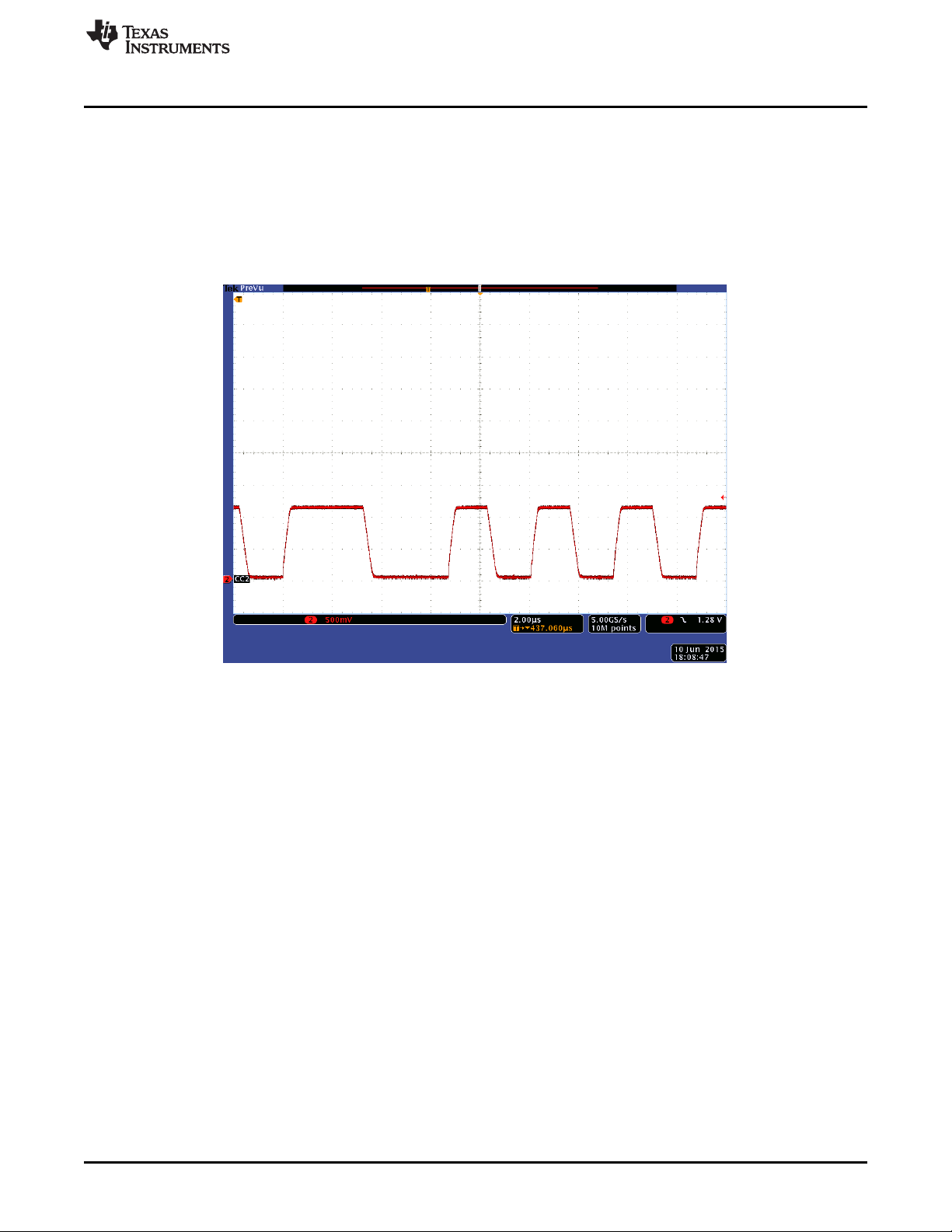
5.1.3.1 TP1 and TP2: CC1/CC2 Test Points
These test points can be used to tie a PD-protocol analyzer for PD BMC data or to verify the BMC signal
integrity with an oscilloscope (depending on the cable orientation). A multimeter or oscilloscope can be
used to measure VCONN when an electronically marked Type-C cable is connected. These test points
are not intended to provide an external load on VCONN. Figure 1 shows the BMC data oscilloscope
capture.
Setup
Figure 1. TPS65981 BMC Data
5.1.3.2 TP3, TP4, TPS, TP7, and TP8: GND Test Points
Two GND test points are provided for attaching an oscilloscope, multimeter, or external load GND. These
test points are connected to the board GND planes through four vias.
SLVUAW8–August 2016
Submit Documentation Feedback
Copyright © 2016, Texas Instruments Incorporated
TPS65981EVM User's Guide
5
Page 6
Setup
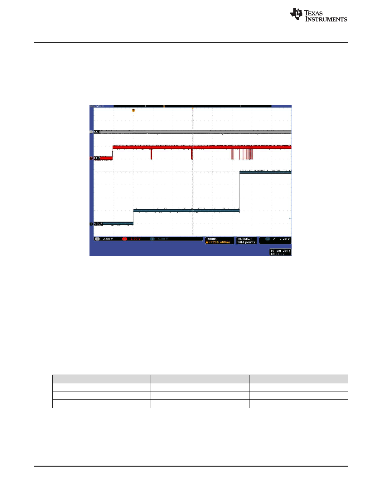
5.1.3.3 TP5: VBUS Test Point
The VBUS test point is used to measure VBUS at the connector. With PD power possibly going up to 20
V, use caution when connecting and disconnecting probes on the TPS65981EVM. The VBUS test point is
capable of drawing up to 3 A for an external load. A PD-power contract with the required capability must
be negotiated to draw current from the VBUS test point. Refer to the TPS6598x Application-Customization
Tool User Guide (SLVUAR8) for configuration instruction. Figure 2 shows the VBUS voltage during PD-
power negotiation.
www.ti.com
Figure 2. TPS65981 VBUS Voltage Transition
5.1.3.4 TP9 and TP10: 5V and 3.3V Test Points
These test points can be used to measure the output voltage of the DC-DC converters that produce the
required functionality of the voltage rails including power delivery, the TPS65981, LEDs, and more.
5.1.4 LED Indicators
5.1.4.1 MXCTL0-2 LEDs (Super-Speed Mux Contol LED)
These LEDs correspond to the GPIOs required to drive a super-speed mux for the SSTX/RX signals to a
Type-C connector. Table 1 lists the LED behavior according to the type of connection.
Table 1. MXCTLx LED Functions
LED Indicator GPIO Function
MXCTL0 GPIO 0 Type-C Connection
MXCTL1 DEBUG1 (GPIO 15) HD3SS460 POL
MXCTL2 GPIO 3 HD3SS460 AMSEL
6
TPS65981EVM User's Guide
Copyright © 2016, Texas Instruments Incorporated
SLVUAW8–August 2016
Submit Documentation Feedback
Page 7
www.ti.com
5.1.4.2 Var DC-DC Enable
This LED is high when the variable DC-DC converter is on which occurs when SYS_PWR is
approximately 20 V.
5.1.4.3 PDO LED 0 and PDO LED 1
These LEDs are high depending on which high-voltage PDO is negotiated. Table 2 lists the LED behavior.
PDO PDO LED 1 PDO LED 0
PDO 1 (5 V) 0 0
PDO 2 (9 V) 0 1
PDO 3 (15 V) 1 0
PDO 4 (20 V) 1 1
6 Using the TPS65981EVM
This section describes the EVM configurations on the preloaded firmware, getting started, and debugging
the EVM.
6.1 Powering the TPS65981EVM
The main power supply for the EVM is J1 barrel jack, which accepts 19 V to 20 V through a barrel jack
adaptor. The EVM can also be powered with an external power supply on J6. The input voltage can range
from 12 V to 20 V, but the appropriate power profile should be configured in the firmware using the
configuration tool. The EVM can also be powered from a TI MCU LaunchPad Development Kit by placing
0-Ω resistors (see Figure 18). If powering with a LaunchPad Development Kit, the EVM does not support
high-voltage contracts or provide high currents at 5 V because of the limited power capability. The EVM
can also be bus powered from the Type-C connector and accepts 5 V to 20 V on VBUS, depending on the
sink configuration.
Using the TPS65981EVM
Table 2. PDO LED Functions
6.2 Firmware Configurations
The EVM is shipped with a preloaded firmware image that supports various Type-C and PD products:
dock and notebook. The firmware is loaded at start-up and the configuration is defined by the state of the
third switch on the S1 configuration switch (see Section 5.1.1.1). The top three switches in the switch bank
represent B0, B1, and B2, respectively. Table 3 lists the configurations on the EVM.
CFG
ID
0
1
Switch S1
0 → ■
0 → ■
0 → ■
0 → ■
0 → ■
0 → ■
■ ← 1
0 → ■
Port Type
Data Power A
DRP
Rp/Rd
DRP
Rp/Rd
Table 3. Firmware Configurations
Type-C
Power
V atAV atAV atAV atAV atAV at
3 5at 3 9at 3
5 at
3
0.9
PD Source
15 at320 at35 at
— — —
PD Sink
Capabilities
A
—
0.9
12 to
5 at
20 at
3
3
DP Support
UFP_D
Config C and D
DFP_D
Config C, D and E
PD Control
Initiated DR/PR Swaps
Initiate DR swap to UFP
Initiate PR swap to Src
Initiate DR swap to DFP
Initiate PR swap to Snk
Application
Docking system
Notebook
system
SLVUAW8–August 2016
Submit Documentation Feedback
Copyright © 2016, Texas Instruments Incorporated
TPS65981EVM User's Guide
7
Page 8
TPS65981EVM
DP-EXPANSION-EVM
(Source)
Notebook
(DP and USB
Source)
USB Source
DP Source
Type-C to Type-A Flash Drive
Notebook with
TPS6598x Utilities
GUI
(Connected with
Type-A)
TPS65981EVMType-A to Type-C Cable
Using the TPS65981EVM
6.3 Connecting the TPS65981EVM
Various Type-C cables can be used to connect the EVM to a legacy Type-A host, legacy Type-A device,
or Type-C device.
6.3.1 Connecting to a Legacy Type-A Host
Using a Type-A plug to Type-C cable allows connection to a legacy host. When the billboarding and
endpoint functions are enabled on the EVM, the user can access the registers and update the firmware by
using the TPS6598x Utilities GUI. The EVM can be powered from the Type-A to Type-C cable and does
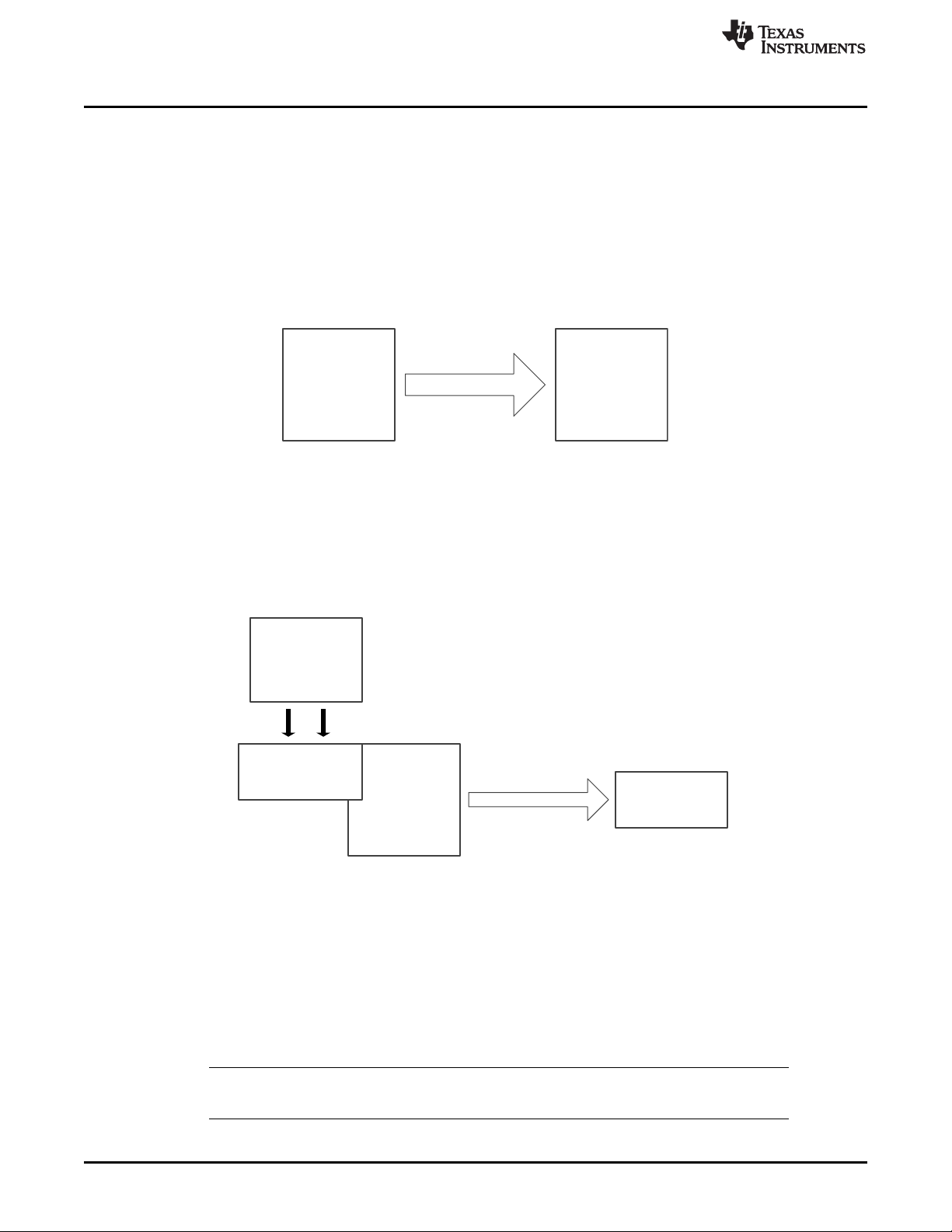
not require a power-supply function with the TPS6598x Utilities GUI. Figure 3 shows how the TPS65981
device is connected to a notebook with the TPS6598x Utilities GUI.
Figure 3. Connecting EVM to Legacy Host
6.3.2 Connecting to a Legacy Type-A Device
Using a Type-C to Type-A receptacle cable allows for connection to a legacy USB device, such as a flashdrive. The TPS65981 device cannot act as a host but can pass the USB connection to a host by using the
DP-EXPANSION-EVM (DisplayPort source board). Figure 4 shows how the notebook, DP-EXPANSIONEVM, TPS65981EVM, cable, and flash drive are connected
www.ti.com
Figure 4. Connecting EVM to Type-A Device
6.3.3 Connecting to Type-C Devices
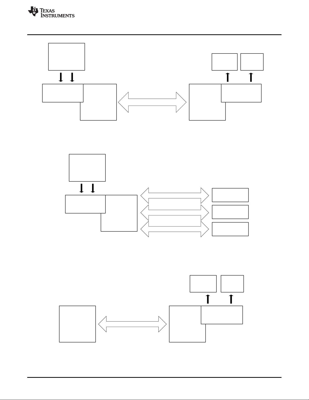
Using a Type-C cable allows for connection to a Type-C device or host. When two TPS65981EVMs are
used with the DP-EXPANSION-EVM (source and sink boards), a complete Type-C system can be verified.
The DisplayPort alternate mode is entered when the two setups appropriately configure as defined in
Table 3. The source setup requires a USB source with DisplayPort to provide data to the sink board. A
monitor can be connected to sink board, along with a USB device to connect to the source board. Figure 5
shows how the boards are connected.
NOTE: Signal integrity can be a factor on USB and DisplayPort video quality because of going
8
TPS65981EVM User's Guide
through multiple connectors and cables.
Copyright © 2016, Texas Instruments Incorporated
SLVUAW8–August 2016
Submit Documentation Feedback
Page 9
Type-C Notebook
(MacBook/
ChromeBook)
TPS65981EVM
DP-EXPANSION-EVM
(Sink)
Monitor
(DisplayPort)
USB
Device
USB SinkDP SInk
Type-C Cable
Type-C Cable
TPS65981EVM
DP-EXPANSION-EVM
(Source)
Notebook
(DP and USB
Source)
USB Source
DP Source
Type-C to Type-A Cable
Type-C to DP/HDMI Dongle
Type-C
Docking System
Type-A
Flash Drive
Monitor
Connection Options
TPS65981EVM
DP-EXPANSION-EVM
(Source)
TPS65981EVM
DP-EXPANSION-EVM
(Sink)
Notebook
(DP and USB
Source)
USB Source
DP Source
Monitor
(DisplayPort)
USB
Device
USB SinkDP SInk
Type-C Cable
www.ti.com
Figure 6 shows how a source setup can be connected to a Type-C device (DisplayPort, USB, or both),
such as a Type-C flash drive, Type-C to DisplayPort dongle, Type-C to HDMI, or Type-C docking system.
Using the TPS65981EVM
Figure 5. Connecting EVM to EVM for Type-C System
Figure 7 shows how a sink setup can be connected to a Type-C host, such as MacBook or ChromeBook
Pixel, to enter the DisplayPort alternate mode. The sink allows DisplayPort and USB connections to the
notebooks.
SLVUAW8–August 2016
Submit Documentation Feedback
Figure 6. Connecting EVM to Type-C Devices
Figure 7. Connecting EVM to Type-C Host
Copyright © 2016, Texas Instruments Incorporated
TPS65981EVM User's Guide
9
Page 10
Using the TPS65981EVM
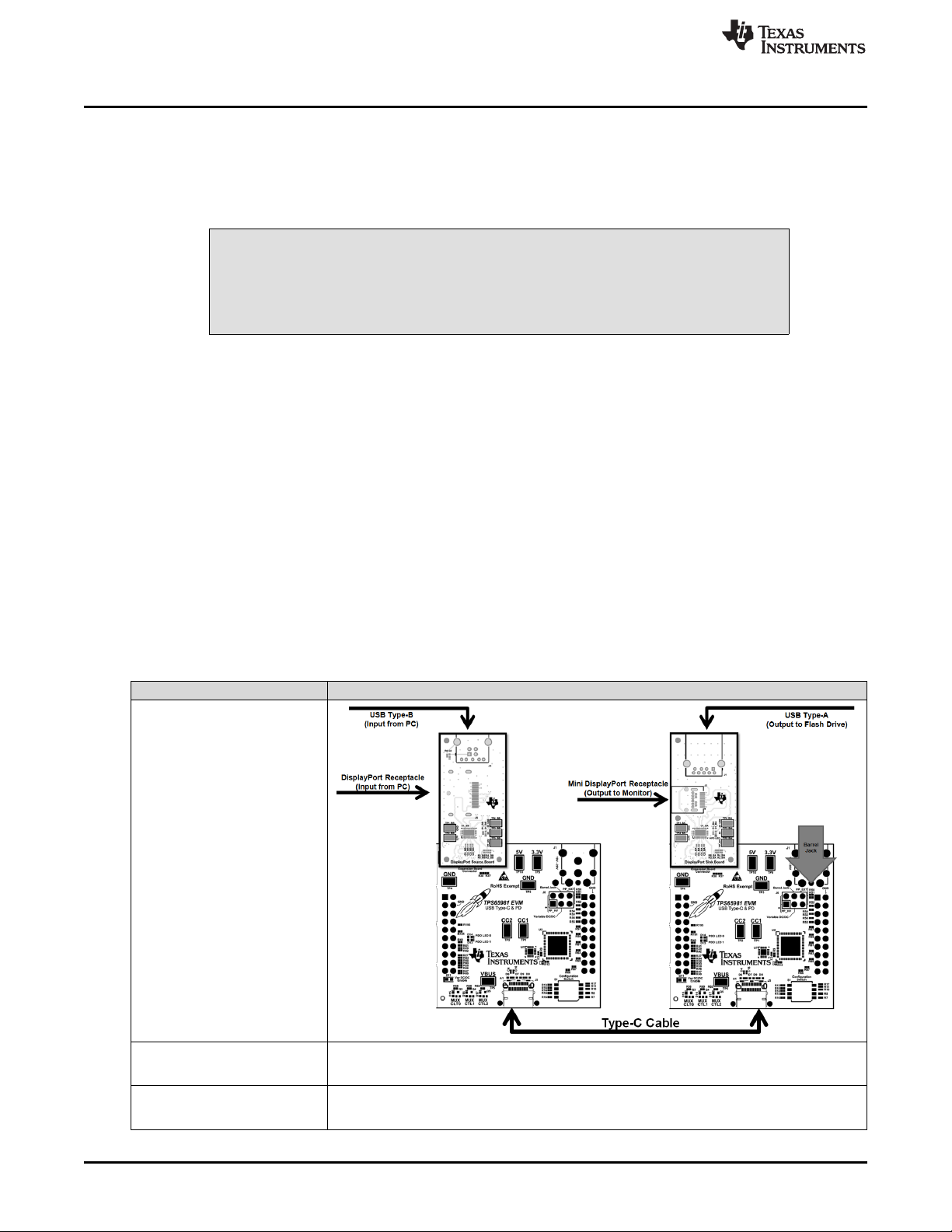
6.3.4 Testing DisplayPort Alternate Mode
The DisplayPort alternate mode can be tested with a non-Type-C notebook, allowing the user to simulate
a DisplayPort DFP_D (video source) or UFP_D (video sink). Table 4 lists the testing flow used to verify
DisplayPort functionality with two TPS65981EVMs and the DP-EXPANSION-EVM (DIsplayPort source
and sink boards).
Do not connect the DP-EXPANSION-EVM to the TPS65981EVM when the
barrel jack is connected—this may result in a short if the expansion board
connectors are misaligned.
The required hardware is listed as follows:
• A Windows PC with a USB Type-A receptacle and DisplayPort video output
– USB3.0 Type-A to Type-B cable
– USB3.0 flash drive
– USB2.0 Type-A to Type-B cable
• USB Type-C Cable
• 1080p Monitor with DisplayPort input
• Mini DisplayPort to DisplayPort cable
• On board FTDI or Aardvark I2C/SPI Host Adapter (Used for programming the TPS695986-EVM and
interfacing with Utilities GUI)
• ACS002 DP-EXPANSION-EVM (source and sink board)
• Two TPS65981EVMs with base firmware (preloaded before shipping)
• Dell laptop power-supply model: DA130PE1-00
www.ti.com
CAUTION
Table 4. DisplayPort Testing Table
Test Step Pass Criteria
Left switch setting:
0 → ■
0 → ■
■ ← 1
0 → ■
Right switch setting:
0 → ■
0 → ■
0 → ■
0 → ■
Connect the ACS002 DisplayPort
source board to board on left output of
the PC and USB3.0 output of the PC.
Connect the ACS002 DisplayPort sink
board to board on right of the monitor
and to a USB3.0 flash drive.
DisplayPort source board should be connected to the DisplayPort
DisplayPort sink board should be connected to the DisplayPort input
10
TPS65981EVM User's Guide
SLVUAW8–August 2016
Submit Documentation Feedback
Copyright © 2016, Texas Instruments Incorporated
Page 11

www.ti.com
Test Step Pass Criteria
Connect the barrel jack to the device
under test (DUT)
Connect the Type-C Cable from the
DUT to the Tester with Texas
Instruments Logo facing DOWN on
both
Check for video on DisplayPort
monitor and verify USB flash drive is
accessible
Verify the voltages on the DUT
DisplayPort source and sink boards
6.4 Debugging the EVM
This section describes various debugging examples.
Using the TPS65981EVM
Table 4. DisplayPort Testing Table (continued)
Variable DC-DC LED (blue LED) will turn ON
DUT LEDs Test LEDs
MXCTL0: ON MXCTL1: ON
MXCTL1: ON MXCTL2: ON
MXCTL2: ON MXCTL3: ON
Variable DC-DC: ON Variable DC-DC: ON
PDO 0: ON PDO 0: OFF
PDO 1: ON PDO 1: OFF
Successfully copy and paste a file to and from the USB flash drive. Extend the PC to the DisplayPort monitor
and play video to verify video stream.
DUT DisplayPort Source Board Tester DisplayPort Sink Board
TP2_BB: 3.3 V TP2_BB: 3.3 V
TP3_BB: 5 V TP3_BB: 5 V
TP4_BB: 5 V TP4_BB: 5 V
TP5_BB: 19 V to 20 V TP5_BB: 5 V
NOTE: The testing and debugging approaches on the EVM can be applied to an actual system to
help identify any issues.
6.4.1 Connection Not Established
The following checks can help resolve issues when connecting the EVM to another Type-C device or EVM
and no status LEDs are on:
• Verify that a firmware image is loaded in on the TPS65981 device using the TPS6598x Utilities GUI.
• Verify the CC lines are toggling for dual-role port functionality (see Figure 8).
• Verify the following system supplies:
– VIN_3V3: 3.3 V
– LDO_3V3: 3.3 V
– LDO_1V8D/A: 1.8 V
– PP_5 V0/PP_CABLE: 5 V
– Barrel Jack: 20 V
• Verify that the devices connected are compatible (see Table 3). Some of the compatible connections
are listed as follows:
– Dual Role Port → UFP
– Dual Role Port → DFP
– DFP → UFP
• Verify that VBUS is reaching 5 V when connected (see Figure 9)
.
SLVUAW8–August 2016
Submit Documentation Feedback
Copyright © 2016, Texas Instruments Incorporated
TPS65981EVM User's Guide
11
Page 12

Using the TPS65981EVM
www.ti.com
Figure 8. DRP CC1 and CC2 Toggling
6.4.2 Reseting Behavior
Improper configurations and shorts can cause a Type-C PD system to constantly reset. Use the following
checks to debug these types of issues:
• Verify that the required power paths have the correct voltages:
– PP_5 V0/PP_CABLE: 5 V
– PP_HV: 20 V (or appropriately configured voltage)
• Probe VBUS, CC1, and CC2 to check for any anomalies. Figure 10 shows a successful power
contract.
• When a short occurs on VBUS, the initial 5 V on VBUS is not present.
• Check for a small spike during a cable attach event to verify that the 5-V switch is closed and is
opened once the overcurrent event is detected.
Figure 9. Type-C Connection and VBUS
12
TPS65981EVM User's Guide
Figure 10. Type-C Connection and PD Negotiation
Copyright © 2016, Texas Instruments Incorporated
SLVUAW8–August 2016
Submit Documentation Feedback
Page 13

www.ti.com
7 Programming the TPS65981EVM Firmware
This section describes loading firmware onto the TPS65981EVM.
NOTE: Other methods of firmware loading are available and are discussed in the TPS6598x Utilities
Tool User Guide.
Step 1. Connect the USB Type-A to micro-B cable from the computer to the TPS65981EVM.
Step 2. Open the TPS6598x Utilities GUI, click the Configure link on the left side of the GUI, verify
the settings, and confirm the connection by clicking the Test Configuration Settings button
(see Figure 11).
Programming the TPS65981EVM Firmware
Step 3. Wait until the results are displayed in the Connection Results section. An EVM that does not
have firmware displays BOOT after the Mode Register returns field.
Step 4. Click the Save Settings as Default button to save configuration settings.
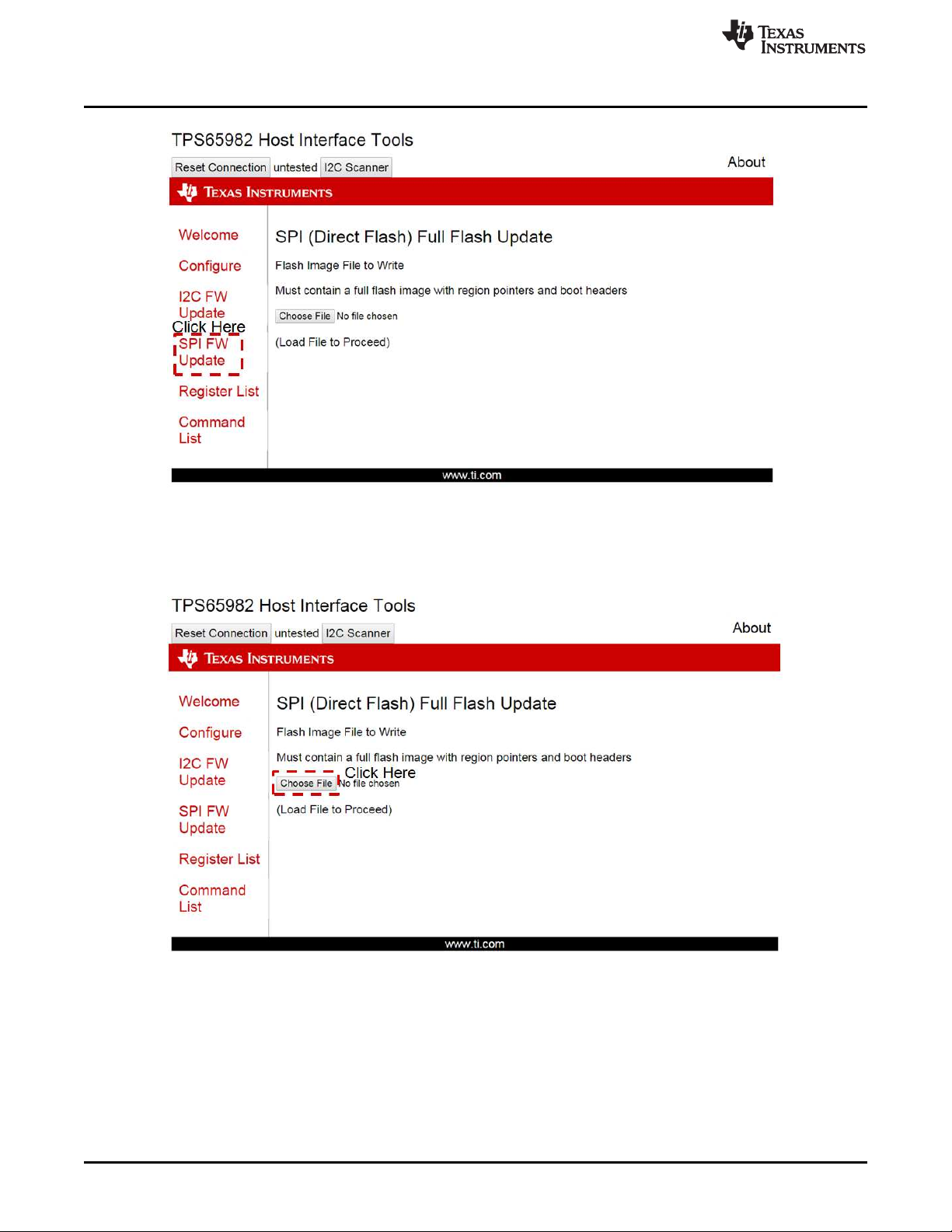
Step 5. Click the SPI FW Update link on the left side of the GUI (see Figure 12).
SLVUAW8–August 2016
Submit Documentation Feedback
Figure 11. FTDI Configuration Settings
Copyright © 2016, Texas Instruments Incorporated
TPS65981EVM User's Guide
13
Page 14
Programming the TPS65981EVM Firmware
Figure 12. SPI Firmware Update Screen
Step 6. Choose the TPS65981EVM firmware image to load by clicking on the Choose File button
(see Figure 13). Select the appropriate EVM image (2 region binary file) in the window and
verify that it is 191KB in size. Click Open to load the file to the TPS6598x Utilities GUI.
www.ti.com
14
Figure 13. SPI Firmware Update – Choose File
Step 7. Click the Program Flash Image (see Figure 14).
TPS65981EVM User's Guide
Copyright © 2016, Texas Instruments Incorporated
SLVUAW8–August 2016
Submit Documentation Feedback
Page 15

www.ti.com
Programming the TPS65981EVM Firmware
Figure 14. SPI Firmware Update – Start Flash Update
Step 8. Wait until the programming process is complete. Verify that the firmware was successfully
loaded. Figure 15 shows a successful firmware update.
Figure 15. SPI Firmware Update – Firmware Update Complete
Step 9. 8. Power cycle the EVM to load the new firmware image.
Step 10. On the TPS6598x Utilities GUI, click the Register List link on the left side of the GUI and
then click the MODE button (see Figure 16). This register will check the I2C communication
and verify that the firmware was loaded on the EVM.
SLVUAW8–August 2016
Submit Documentation Feedback
Copyright © 2016, Texas Instruments Incorporated
TPS65981EVM User's Guide
15
Page 16

Programming the TPS65981EVM Firmware
www.ti.com
Figure 16. Register List
Step 11. Verify the that the MODE register reads APP (see Figure 17).
Figure 17. Mode Register
16
TPS65981EVM User's Guide
Copyright © 2016, Texas Instruments Incorporated
SLVUAW8–August 2016
Submit Documentation Feedback
Page 17

SWD_DATA
SWD_CLK
I2C_IRQ1Z
GPIO5
GPIO0
GPIO4_HPD
SPI_MOSI
SPI_MISO
SPI_CLK
SPI_SSZ
MRESET
LDO_3V3
AUX_P
AUX_N
P3V3
P5V
DEBUG_CTL1
DEBUG_CTL2
GPIO3
RESETZ
GPIO6
GPIO2
DEBUG1
I2C_SDA1
I2C_SCL1
ISENSE_VOUT
HV_GATE_1
HV_GATE_2
IVBUS_SENSE_N
V_SENSE_OUT VCC
IVBUS_SENSE_P
IVIN_3V3_P
IVIN_3V3_N
U_ACS005E2_Current_Sense
ACS005E2_Current_Sense.SchDoc
F_I2C_SDA1
F_I2C_SCL1
F_RESETN
FS_SPI_CLK
FS_SPI_MISO
FS_SPI_MOSI
FS_SPI_CSZ
U_ACS005E2_FTDI
ACS005E2_FTDI.SchDoc
C_CC1
C_CC2
RESETZ
MRESET
USB2_RP_P
USB2_RP_N
AUX_P
AUX_N
DEBUG1
SWD_DATA
SWD_CLK
I2C_IRQ1Z
I2C_SDA1
I2C_SCL1
GPIO8
GPIO7
GPIO6
GPIO4_HPD
GPIO3
GPIO2
GPIO0
SPI_MOSI
SPI_MISO
SPI_CLK
SPI_SSZ
VBUS_SENSE
DEBUG_CTL1
DEBUG_CTL2
LDO_3V3
PP_EXT
GPIO5
BUSPOWERZ
LDO_1V8
USB_T_P
USB_T_N
USB_B_P
USB_B_N
SBU_P
SBU_N
HV_GATE_2
HV_GATE_1
P5V0
U_ACS005E2_Processor
ACS005E2_Processor.SchDoc
HPD
LDO_3V3
PPHV
P5V
USB_5V
P3V3
GPIO_0
GPIO_6
GPIO_2
GPIO_3
C_SSRX2_P
C_SSRX2_N
C_SSRX1_P
C_SSRX1_N
C_SSTX2_N
C_SSTX2_P
I2C1_SCL
I2C1_SDA
I2C1_IRQz
AUX_P
AUX_N
USB2_P
USB2_N
DEBUG_2
DEBUG_1
C_SSTX1_P
C_SSTX1_N
U_ACS005E2_Inter_PCB
ACS005E2_Inter_PCB.SchDoc
VBUS
P5V
LDO_3V3
VIN_3V3
PPHV
VBUS_SENSE
IVIN_3V3_P
IVIN_3V3_N
BUSPOWERZ
LDO_1V8
U_ACS005E2_Power_Path
ACS005E2_Power_Path.SchDoc
P3V3
USB_5V
PGood
PDO_0
PDO_1
SYS_PWR
VAR_DCDC
3V3_EN
PLUG_EVENT
U_ACS005E2_Power_Supply
ACS005E2_Power_Supply.SchDoc
C_SSRX1_P
C_SSRX1_N
C_USB_B_N
C_USB_B_P
C_SSTX2_N
C_SSTX2_P
VBUS
C_SSTX1_P
C_SSTX1_N
C_USB_T_P
C_USB_T_N
C_SSRX2_N
C_SSRX2_P
C_CC1
C_CC2
C_SBU_P
C_SBU_N
LDO_3V3
C_VBUS_SENSE_N
C_VBUS_SENSE_P
U_ACS00E2_Type_C
ACS005E2_Type_C.SchDoc
VAR_DCDC
SYS_PWR PP_EXT
PP_HV
U_ACS005E2_Power_Jumper
ACS005E2_Power_Jumper.SchDoc
P3V3
P5V0
SYS_PWR
P3V3
P5V0
LDO_3V3
SYS_PWR
GPIO_2
GPIO_2
GPIO_7
GPIO_8
C_USB_T_N
C_USB_T_P
C_USB_B_P
C_USB_B_N
C_SSRX2_P
C_SSRX2_N
C_SSRX1_P
C_SSRX1_N
C_SSTX2_P
C_SSTX2_N
C_SSTX1_P
C_SSTX1_N
AUX_P
AUX_N
USB2_N
USB2_P
VBUS_SENSE
PP_HV
PP_EXT
LDO_3V3
Copyright © 2016, Texas Instruments Incorporated
www.ti.com
8 TPS65981EVM Schematic
SLVUAW8–August 2016
Submit Documentation Feedback
Figure 18 shows the block diagram of the main components of the TPS65981EVM.
Figure 18. TPS65981EVM Block Diagram
Copyright © 2016, Texas Instruments Incorporated
TPS65981EVM Schematic
TPS65981EVM User's Guide
17
Page 18

GND
0.22µF
C5
15.0kR5
GND
GND
CS
1
DO/IO1
2
WP/IO2
3
GND
4
DI/IO0
5
CLK
6
HOLD/IO3
7
VCC
8
U1
W25Q80DVSNIG
3.3k
R1
3.3k
R2
GND
GND
0.1µF
C1
3.3kR33.3k
R4
C_CC1
C_CC2
RESETZ
MRESET
USB_T_P
USB_T_N
USB_B_P
USB_B_N
SBU_P
SBU_N
USB2_RP_P
USB2_RP_N
AUX_P
AUX_N
DEBUG1
GND
100k
R22
100k
R21
SWD_DATA
SWD_CLK
I2C_IRQ1Z
I2C_SDA1
I2C_SCL1
GPIO8
GPIO7
GPIO6
GPIO4_HPD
GPIO3
GPIO2
63
1 8
2 7
54
S1
100k
R13
100k
R14
100k
R15
100k
R16
GPIO0
0R9
0R12
SPI_MOSI
SPI_MISO
SPI_CLK
SPI_SSZ
LDO_3V3
LDO_3V3
VBUS_SENSE
DEBUG_CTL1
DEBUG_CTL2
11.0kR7
11.0kR8
11.0kR10
11.0kR11
I2C_SCL1
I2C_SDA1
I2C_IRQ1Z
3.83kR27
3.83kR28
10.0kR29
LDO_3V3
LDO_3V3
1.00M
R23
1.00M
R24
1.00M
R25
1.00M
R26
GND
LDO_3V3
GND
GND
A2A1
B2B1
C2
C1
D2D1
E2E1
Q8
CSD87501L
0.005
R94
SENSEP
SENSEN
HV_GATE2
HV_GATE1
SENSEN
SENSEP
HV_GATE2HV_GATE1
PP_EXT
AUX_N
55
AUX_P
54
C_CC1
13
C_CC2
15
C_SBU1
10
C_SBU2
11
C_USB_BN
9
C_USB_BP
8
C_USB_TN
7
C_USB_TP
6
DEBUG1
2
DEBUG_CTL1
45
DEBUG_CTL2
44
GPIO0
41
GPIO2
25
GPIO3
19
GPIO4
26
GPIO5
23
GPIO6
20
GPIO7
38
GPIO8
1
HV_GATE1
31
HV_GATE2
32
I2C_IRQ1
43
I2C_SCL1
47
I2C_SDA1
46
MRESET
24
RESET
21
RPD_G1
12
RPD_G2
16
R_OSC
52
SENSEN
29
SENSEP
30
SPI_CLK
37
SPI_CS
39
SPI_MISO
35
SPI_MOSI
36
SS
3
SWD_CLK
50
SWD_DAT
49
USB_RP_N
5
USB_RP_P
4
U2:1
TPS65981ABQWRWERQ1
GPIO5
BUSPOWERZ
11.0kR17
LDO_1V8
I2C_SCL1
I2C_SDA1
I2C_IRQ1Z
DEBUG1 = MX_CTL1 = POL
GPIO7 = PDO_TT_0
GPIO8 = PDO_TT_1
GPIO3 = MX_CTL2 = AMSE L(HD3SS460)
GPIO0 = MX_CTL0_EN (HD3SS460)
GPIO0 = MX_CTL0_USB3 (TUSB546)
GPIO3 = MX_CTL2 = DP_M ODE (TUSB546)
DEBUG1 = MX_CTL1 = POL
GPIO2 = BARREL_JACK_DETEC T
0
R18
HV_GATE_2
HV_GATE_1
SPI_MISO
SPI_MOSI
SPI_CSZ
SPI_CLK
3
2
1
Q3
2.00k
R58
GND
White
1
2
D15
3
2
1
Q4
2.00k
R60
GND
White
1
2
D16
3
2
1
Q5
2.00k
R62
GND
White
1
2
D17
MX_CTL0
MX_CTL1
MX_CTL2
MX_CTL0 MX_CTL1 MX_CTL2
P5V0
220pF
C2
220pF
C3
Copyright © 2016, Texas Instruments Incorporated
TPS65981EVM Schematic
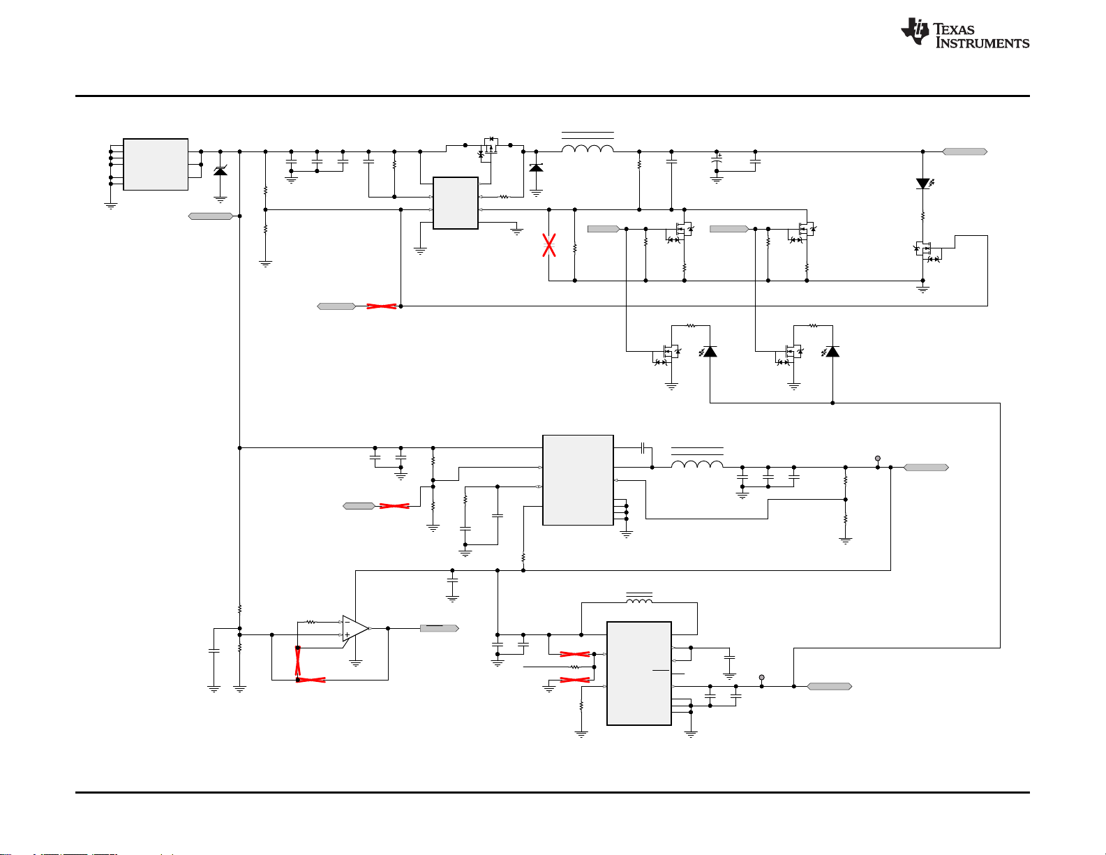
Figure 19 shows the processor block, which contains the TPS65981 PD protocol functions, flash for the TPS65981 device, S2 for the firmware
configuration, and the required passives.
www.ti.com
Figure 19. TPS65981EVM Processor Block
18
TPS65981EVM User's Guide
Copyright © 2016, Texas Instruments Incorporated
SLVUAW8–August 2016
Submit Documentation Feedback
Page 19

VREGIN
50
VREGOUT
49
DM
7
REF
6
RESET#
14
EECS
63
EECLK
62
EEDATA
61
OSCI
2
OSCO
3
ADBUS0
16
VPHY
4
VPLL
9
VCORE
12
VCCIO
20
AGND
10
GND
1
SUSPEND#
36
PWREN#
60
TEST
13
DP
8
ADBUS1
17
ADBUS2
18
ADBUS3
19
ADBUS4
21
ADBUS5
22
ADBUS6
23
ADBUS7
24
BDBUS0
26
BDBUS1
27
BDBUS3
29
BDBUS2
28
BDBUS4
30
BDBUS5
32
BDBUS6
33
BDBUS7
34
CDBUS0
38
CDBUS1
39
CDBUS2
40
CDBUS3
41
CDBUS4
43
CDBUS5
44
CDBUS6
45
CDBUS7
46
DDBUS0
48
DDBUS1
52
DDBUS2
53
DDBUS3
54
DDBUS4
55
DDBUS5
57
DDBUS6
58
DDBUS7
59
GND
5
GND
11
GND
15
GND
25
GND
47
GND
51
VCORE
37
VCORE
64
VCCIO
31
VCCIO
42
VCCIO
56
GND
35
U11
FT4232HL
GND
GND
VBUS
1
D-
2
D+
3
ID
4
GND
5
678
9
10
J13
ZX62RD-AB-5P8
1
2
12MHz
Y1
ECS-120-20-3X-TR
27pF
C63
27pF
C62
VSS
2
DI
3
VCC
6
CS
5
CLK
4
DO
1
U14
93LC56B-I/OT
2.20k
R204
GND
0.1µF
C50
GND
10.0k
R121
10.0k
R120
10.0k
R119
GND
0
R165
12kR152
GND
0.1µF
C57
0.1µF
C58
0.1µF
C59
0.1µF
C60
0.1µF
C53
0.1µF
C51
0.1µF
C54
0.1µF
C55
0.1µF
C56
GND
GND
GND
GND
GND
GND
0R126
0R131
0R146
0R137
0R139
0R136
0R125
0R123
0R129
0R132
0R138
0R141
0R144
0R148
0R130
0R133
0R135
0R145
0R149
1 2
3 4
5 6
7 8
9 10
J14
0R183
0R184
0R186
0R188
0R190
0R189
1 2
3 4
5 6
7 8
9 10
J11
0R162
0R168
0R170
0R163
1
EN
2
IN
3
IN
4
OUT
5
OUT
6
NC
7
PG
8
GND
U13 TPS76833QD
0.1µF
C65
GND
GND
GND
249k
R203
10µF
C66
DNPR181
DNPR182
Aardvark Connector
GND
0
R172
0
R192
GND
ULINK2 Debugger
DNPR175
DNPR173
DNPR171
DNPR169
DNPR167
DNPR166
DNPR164
DNPR161
DNPR159
DNPR158
DNPR157
DNPR155
DNPR154
DNPR153
DNPR140
GNDGND
GND
DNPR128
3.3kR176
10kR180
3.3kR177
3.3kR178
3.3kR179
10kR174
Connectors
DNPR143
DNPR147
DNPR150
DNPR151
GND
TP7
GND
TP8
GND
D+1D-
2
GND
3
U12
TPD2E009DRTR
GND
0R142
0R127
0R122
0R124
0
R210
4.7µF
C52
4.7µF
C49
4.7µF
C61
GND
26 ohmL5
0.01µF
C64
0R134
1.00k
R156
F_SPI_CLK
F_SPI_MOSI
F_SPI_MISO
F_SPI_CSZ
F_I2C_SCL1
F_I2C_SDA1
F_I2C_SCL1
F_I2C_SDA1
F_SPI_CLK
F_SPI_CSZ
F_SPI_MISO
F_SPI_MOSI
F_SPI_CSZ
F_I2C_SCL1
F_I2C_SDA1
F_I2C_IRQ1
F_I2C_IRQ2
F_I2C_SCL2
F_I2C_SDA2
F_I2C_SCL2
F_I2C_SDA2
F_I2C_SCL1
F_I2C_SDA1
F_SPI_CLK F_SPI_MOSI
F_SPI_MISO
F_SPI_CSZ
F_I2C_IRQ2
F_I2C_SCL2
F_I2C_SDA2
F_SYSTEM_3V3
F_SYSTEM_3V3
F_SYSTEM_3V3
F_SYSTEM_3V3
F_SYSTEM_3V3
F_SYSTEM_3V3
F_SYSTEM_3V3
F_SYSTEM_3V3
F_SYSTEM_3V3
F_SYSTEM_3V3 F_SYSTEM_3V3
F_SYSTEM_3V3
F_5V_VBUS
F_5V_VBUS
F_5V_VBUS
F_SWD_DATA
F_SWD_CLK
F_SWD_CLK
F_SWD_DATA
VREGOUT
VREGOUT
F_USB_D_P
F_USB_D_N
F_USB_D_P
F_USB_D_N
F_USB_D_P F_USB_D_N
EECS
EECLK
EEDATA
EECS
EECLK
EEDATA
EECS
EECLK
EEDATA
EEDATA
F_RESETN
RESETN
F_D_UART_TX
F_D_UART_RX
F_C_UART_RX
F_C_UART_TX
F_C_UART_RX
F_C_UART_TX
F_D_UART_TX
F_D_UART_RX
F_D_UART_TX
F_D_UART_RX
F_A_GPIO_0
F_A_GPIO_1
F_A_GPIO_2
F_A_GPIO_3
F_B_GPIO_0
F_B_GPIO_1
F_B_GPIO_2
F_B_GPIO_3
F_A_GPIO_0
F_A_GPIO_1
F_A_GPIO_2
F_I2C_SCL1
F_I2C_SDA1
F_SPI_CLK
F_SPI_MOSI
F_SPI_MISO
F_SPI_CSZ
F_I2C_SDA1
F_I2C_SCL1
F_RESETN
F_RESETN
1
3
5 6
4
2
7
9 10
8
1211
1413
1615
1817
2019
J8
CRD-081413-A-G
1
3
5 6
4
2
7
9 10
8
1211
1413
1615
1817
2019
J9
CRD-081413-A-G
124
3
S2
63
1 8
2 7
54
S4
0R33
0R35
0R39
0R43
FS_SPI_CLK
FS_SPI_MISO
FS_SPI_MOSI
FS_SPI_CSZ
63
1 8
2 7
54
S3
F_RESETN RESETN
100k
R160
GND
10µF
C67
F_I2C_IRQ1
Copyright © 2016, Texas Instruments Incorporated
www.ti.com
Figure 20 shows the FTDI block, which contains circuitry for the USB and Aardvark to SPI or I2C interface.
SLVUAW8–August 2016
Submit Documentation Feedback
Figure 20. FTDI Block
Copyright © 2016, Texas Instruments Incorporated
TPS65981EVM Schematic
TPS65981EVM User's Guide
19
Page 20

-IN
1
GND
2
REF2
3
NC
4
OUT
5
V+
6
REF1
7
+IN
8
U8
INA284AIDGKR
IVBUS_SENSE_N
V_SENSE_OUT
VCC
IVBUS_SENSE_P
IVIN_3V3_P
IVIN_3V3_N
0.1µF
C70
GND
GND
0 R90
0 R93
0 R111
0 R92
0 R91
Copyright © 2016, Texas Instruments Incorporated
1 2
3 4
5 6
J6
VAR_DCDC SYS_PWR
PP_HV
PP_EXT
Copyright © 2016, Texas Instruments Incorporated
TPS65981EVM Schematic
Figure 21 shows the power-jumper connector, which allows the user to connect the power paths according to the firmware configuration.
Figure 22 shows the optional current-sense circuitry for VBUS and VIN_3V3.
www.ti.com
Figure 21. Power Jumper Block
20
TPS65981EVM User's Guide
Figure 22. Current-Sense Block
Copyright © 2016, Texas Instruments Incorporated
SLVUAW8–August 2016
Submit Documentation Feedback
Page 21

21 ohm
L1
GND
1µFC17
0.1µF
C15
GND
1µFC7
GND
1µF
C6
VBUS
P5V
22µF
C14
LDO_3V3
VIN_3V3
PPHV
VBUS_SENSE
TP3
GND
TP4
GND
IVIN_3V3_P
IVIN_3V3_N
0.51R88
I_3V3_N
BUSPOWER
22
LDO_1V8A
56
LDO_1V8D
40
LDO_BMC
48
PAD
57
PP_5V0
28
PP_5V0
27
PP_CABLE
14
PP_HV
34
PP_HV
33
VBUS
17
VDDIO
42
VIN_3V3
53
VBUS
18
LDO_3V3
51
U2:2
TPS65981ABQWRWERQ1
GND
10µFC18
1µFC20
1µFC19 LDO_1V8A
GND GND
GND
BUSPOWERZ
LDO_1V8
0.1µF
C13
10µF
C12
Copyright © 2016, Texas Instruments Incorporated
www.ti.com
Figure 23 shows the power path block of the TPS65981 and the required passives.
TPS65981EVM Schematic
Figure 24 shows the power-supply block, which has all of the board supplies generated and the comparator circuit for barrel jack detection. The
P3V3 rail is on in bus-powered and self-powered conditions, and it has the ability to operate at 4 V to compensate for IR drop through the Type-C
cable. The P5V supply can operate at 4.5 V at 100% duty cycle, but it is intended to supply the 5 V at 3 A when the barrel jack (J4) is connected to
the EVM only. USB_5V is supplied by a boost converter from the main 3.3-V rail and is intended to ensure there is 5 V for the USB DFP port on
the DP-EXPANSION_EVM, when acting bus-powered or self-powered.
SLVUAW8–August 2016
Figure 23. TPS65981EVM Power Path Block
Submit Documentation Feedback
Copyright © 2016, Texas Instruments Incorporated
TPS65981EVM User's Guide
21
Page 22
AUX
10
EN
4
ENUSB
7
FAULT
8
GND
5
ILIM
6
IN
3
PGND
2
SW
1
USB
9
PAD
11
U6
TPS2500DRCR
0.1µF
C29
0.1µF
C31
GND
GND
GND
10uH
L3
V3V3_Sense
GND
0.1µF
C39
IMax = 3A
IMax = 1100 mA (adjustable Il im)
GND
GND
GND
ILim set
Max 1100mA
Typ 900mA
Min 700mA
P3V3
USB_5V
3
4
1
6
2
V+
V-
5
U5
TLV3012AIDCKR
560k
R213
39k
R212
GND
GND
Hysterisis
Vh 1.376V
Vl 1.16V
100k
R207
15.0k
R209
GND
Good @ 11.2V
!Good @9.5V
PGood
22pF
C40
GND
2.2µH
L4
0.1µF
C34
0
R208
GND
22µF
C30
VIN
1
VSENSE
6
EN
8
PGOOD
10
GND
3
COMP
7
PH
2
BOOT
9
PAD
11
GND
4
GND
5
U4
TPS54334DRCR
300pF
C35
2.61k
R202
6800pF
C36
GND
PGD_3V3
PGD_3V3
GND
383
R84
22µF
C22
22µF
C23
1000pF
C27
GND
8.2k
R80
GND
GND
100k
R191
PDO_0 PDO_1
PD Contract: 5V
GND
Output capacitors must be rated to
at least 25V and have ESR in 1 00s of mOhms
DCR: 62mOhm
GND
VIN
8
ADJ
5
PGND6GND
2
ISEN
1
PGATE
7
EN3FB
4
U3
LM3489QMM/NOPB
270
R83
D3
1000pF
C28
GND
0.1µF
C26
0.1µF
C24
11.0k
R85
100k
R82
GND
0R86
10uH
L2
3
5,6,84,7
1,2,
Q21
Blue
2
1
D11
SYS_PWR
47µF
C42
47µF
C43
100k
R200
32.4k
R206
100k
R205
150k
R199
66.5k
R201
0R215
32.4k
R214
3
2
1
Q23
3
2
1
Q22
100k
R195
19.1k
R187
18.0k
R194
7.15k
R196
3
2
1
Q25
0.1µF
C25
60.4k
R81
100µF
C21
VAR_DCDC
3V3_EN
0
R6
PLUG_EVENT
D1
GND
SENSE
1
GND
4
POWER
2
POWER
3
GND
5
SHIELD
6
SHIELD
7
SHIELD
8
SHIELD
9
J1
JPD1135-509-7F
GND
100kR211
51.0kR32
GND
TP9
TP10
3
2
1
Q1
3
2
1
Q2
2.00k
R19
2.00k
R20
GND GND
White
1
2
D14
White
1
2
D13
0.1µF
C37
47µF
C32
47µF
C33
47µF
C41
47µF
C38
Copyright © 2016, Texas Instruments Incorporated
TPS65981EVM Schematic
www.ti.com
22
TPS65981EVM User's Guide
Figure 24. TPS65981EVM Power-Supply Block
Copyright © 2016, Texas Instruments Incorporated
SLVUAW8–August 2016
Submit Documentation Feedback
Page 23

GND GND
GNDGND
C_SSRX1_P
C_SSRX1_N
C_USB_B_N
C_USB_B_P
C_SSTX2_N
C_SSTX2_P
VBUS
C_SSTX1_P
C_SSTX1_N
C_USB_T_P
C_USB_T_N
C_SSRX2_N
C_SSRX2_P
GND
A1
TX1+
A2
TX1-
A3
VBUS
A4
CC1
A5
D+
A6
D-
A7
SBU1
A8
VBUS
A9
RX2-
A10
RX2+
A11
GND
A12
GND
B1
TX2+
B2
TX2-
B3
VBUS
B4
CC2
B5
D+
B6
D-
B7
SBU2
B8
VBUS
B9
RX1-
B10
RX1+
B11
GND
B12
H1
H1
H2
H2
H3
H3
H4
H4
H5
H5
H6
H6
11223
3
J5
20-0000016-01
FLT
9
CC1
12
CC2
11
C_CC1
4
C_CC2
5
C_SBU1
1
C_SBU2
2
D1
20
D2
19
D3
17
D4
16
GND
18
GND
13
GND
8
PAD
21
RPD_G1
7
RPD_G2
6
SBU1
15
SBU2
14
VBIAS
3
VPWR
10
U7
TPD8S300RUK
CC1
CC2
C_USB_T_P
C_USB_T_N
100k
R87
1µF
C68
GND
LDO_3V3
0.001
R89
C_VBUS_SENSE_N
C_VBUS_SENSE_P
D2
GND
D9
D6 D7
D8
GND
GND
D12D10
GND
D5D4
C_CC1
C_CC2
C_SBU_P
C_SBU_N
CC1
CC2
SBU_P
SBU_N
C_CC1
C_CC2
C_SBU_P
C_SBU_N
SBU_P
SBU_N
C_USB_T_P
C_USB_T_N
C_USB_B_N
C_USB_B_P
C_USB_B_P
C_USB_B_N
TC_SSTX2_N
TC_SSTX2_P
TC_SSTX1_P
TC_SSTX1_N
0.01µFC80.01µFC90.01µF
C10
0.01µF
C11
GND
TP5
TP1
TP2
GND
0.1µF
C69
0 C45
0 C44
0 C4
0 C16
Copyright © 2016, Texas Instruments Incorporated
www.ti.com
Figure 25 shows the Type-C block, which includes the Type-C connector and ESD protection.
TPS65981EVM Schematic
SLVUAW8–August 2016
Submit Documentation Feedback
Figure 25. TPS65981EVM Type-C Block
Copyright © 2016, Texas Instruments Incorporated
TPS65981EVM User's Guide
23
Page 24

HPD
1
3
5 6
4
2
7
9 10
8
1211
1413
1615
1817
2019
2221
2423
2625
2827
3029
3231
3433
3635
3837
4039
J4
LSEM-120-03.0-F-DV-A-N-K-TR
LDO_3V3
PPHV
P5V
USB_5V
P3V3
GPIO_0
GPIO_6
GPIO_2
GPIO_3
GNDGND
C_SSRX2_P
C_SSRX2_N
C_SSRX1_P
C_SSRX1_N
C_SSTX2_N
C_SSTX2_P
I2C1_SCL
I2C1_SDA
I2C1_IRQz
AUX_P
AUX_N
USB2_P
USB2_N
DEBUG_2
DEBUG_1
C_SSTX1_P
C_SSTX1_N
Removed GPIO7 & 8 (Used for Var DC/DC)EMPTY_GPIO7
EMPTY_GPIO8
Shorted Debug1 & 2 on Block Diagram
POL Signal Coming from Debug 1 on Processor Block
Copyright © 2016, Texas Instruments Incorporated
TPS65981EVM Schematic
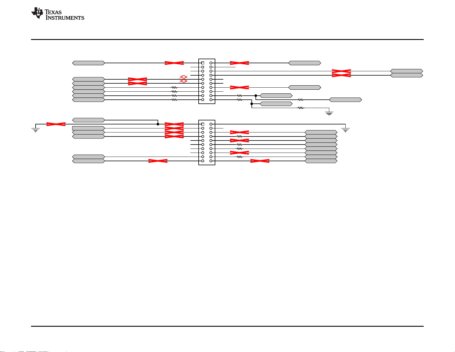
Figure 26 shows the Inter_PCB block, which has the connections that go to the DP-EXPANSION-EVM.
www.ti.com
Figure 26. TPS65981EVM Inter PCB Block
24
TPS65981EVM User's Guide
Copyright © 2016, Texas Instruments Incorporated
SLVUAW8–August 2016
Submit Documentation Feedback
Page 25
0 R59
DNP R57
DNP R63
0 R61
DNP R54
DNP R41
DNP R55 GND
DNP R53
0 R51
DNP R67DNP R66
0 R65
0 R47
0 R45
DNP R56
3.83k
R48
100k R49
GND
DNP R37
DNP R38
0 R40
0 R42
0 R44
0 R46
DNP R36
DNP R34
100k
R50
GND
SWD_DATA
SWD_CLK
I2C_IRQ1Z
GPIO5
GPIO0
GPIO4_HPD
SPI_MOSI
SPI_MISO
SPI_CLK
SPI_SSZ
MRESET
LDO_3V3
AUX_P
AUX_N
P3V3 P5V
DNP R31DNP R30
DEBUG_CTL1
DEBUG_CTL2
GPIO3 RESETZ
GPIO6
GPIO2
DNP R52
DEBUG1
ISENSE_VOUT
I2C_SDA1
I2C_SCL1
GND
GND
1
3
5 6
4
2
7
9 10
8
1211
1413
1615
1817
2019
J3
CRD-081413-A-G
1
3
5 6
4
2
7
9 10
8
1211
1413
1615
1817
2019
J2
CRD-081413-A-G
B_AUX_N
B_AUX_P
HV_GATE_2 HV_GATE_1
Copyright © 2016, Texas Instruments Incorporated
www.ti.com
Figure 27 shows the Debug_Connectors block, which contain the connections to the debug headers.
TPS65981EVM Schematic
Figure 27. TPS65981EVM Debug Connector Block
SLVUAW8–August 2016
Submit Documentation Feedback
Copyright © 2016, Texas Instruments Incorporated
TPS65981EVM User's Guide
25
Page 26

TPS65981EVM Board Layout
9 TPS65981EVM Board Layout
The following figures contain the PCB layouts of the TPS65981EVM.
Figure 28. TPS65981EVM Top Layer Figure 29. TPS65981EVM Top Layer Component View
www.ti.com
Figure 30. TPS65981EVM GND Plane 1 Figure 31. TPS65981EVM Mid Layer 1
Figure 32. TPS65981EVM GND Plane 2 Figure 33. TPS65981EVM Mid Layer 2
26
TPS65981EVM User's Guide
Copyright © 2016, Texas Instruments Incorporated
SLVUAW8–August 2016
Submit Documentation Feedback
Page 27

www.ti.com
TPS65981EVM Board Layout
Figure 34. TPS65981EVM Mid Layer 3 Figure 35. TPS65981EVM GND Plane 3
Figure 36. TPS65981EVM Bottom Layer Figure 37. TPS65981EVM Bottom Layer Component
View
SLVUAW8–August 2016
Submit Documentation Feedback
Copyright © 2016, Texas Instruments Incorporated
TPS65981EVM User's Guide
27
Page 28

TPS65981EVM Bill of Materials
www.ti.com
10 TPS65981EVM Bill of Materials
Table 5 list the bill of materials (BOM) for the TPS65981EVM.
Table 5. BOM
Designator Quantity Value Description Package Reference Part Number Manufacturer
!PCB1 1 Printed Circuit Board ACS005 Any
C1, C15 2 0.1µF CAP, CERM, 0.1 µF, 10 V, ±10%, X5R, 0201 0201 CL03A104KP3NNNC Samsung
C2, C3 2 220pF CAP, CERM, 220 pF, 25 V, ±10%, X7R, 0201 0201 GRM033R71E221KA01D MuRata
C4, C16, C44, C45, R9, R12,
R40, R42, R44, R45, R46,
R47, R56, R59, R61, R65,
R90, R91, R93, R215
C5 1 0.22µF CAP, CERM, 0.22 µF, 6.3 V, ±20%, X5R, 0201 0201 GRM033R60J224ME90 MuRata
C6 1 1µF CAP, CERM, 1 µF, 35 V, ±10%, JB, 0402 0402 C1005JB1V105K050BC TDK
C7, C17, C19, C20 4 1µF CAP, CERM, 1 µF, 10 V, ±20%, X5R, 0201 0201 CL03A105MP3NSNC Samsung
C8, C9, C10, C11 4 0.01µF CAP, CERM, 0.01 µF, 50 V, ±10%, X7R, 0402 0402 GRM155R71H103KA88D MuRata
C12 1 10µF CAP, CERM, 10 µF, 25 V, ±20%, X5R, 0603 0603 GRM188R61E106MA73D MuRata
C13, C37 2 0.1µF CAP, CERM, 0.1 µF, 35 V, ±10%, X5R, 0402 0402 GMK105BJ104KV-F Taiyo Yuden
C14 1 22µF CAP, CERM, 22 µF, 10 V, ±20%, X5R, 0603 0603 GRM188R61A226ME15D MuRata
C18 1 10µF CAP, CERM, 10 µF, 10 V, ±20%, X5R, 0402 0402 CL05A106MP5NUNC Samsung
C21 1 100µF CAP, TA, 100 µF, 25 V, ±10%, 0.15 ohm, SMD 7343-43 T495X107K025ZTE150 Kemet
C22, C23, C30 3 22µF CAP, CERM, 22 µF, 35 V, ±20%, X5R, 0805 0805 C2012X5R1V226M125AC TDK
C24, C25, C26 3 0.1µF CAP, CERM, 0.1 µF, 50 V, ±10%, X7R, 0402 0402 C1005X7R1H104K050BB TDK
C27 1 1000pF CAP, CERM, 1000 pF, 50 V, ±20%, X7R, 0402 0402 C1005X7R1H102M TDK
C29, C31, C39 3 0.1µF CAP, CERM, 0.1µF, 50V, +/-20%, C0G/NP0, 0402 0402 C1005X7R1H104M TDK
C32, C33 2 47µF CAP, CERM, 47 µF, 6.3 V, ±20%, X5R, 0805 0805 GRM21BR60J476ME15L MuRata
C34 1 0.1µF CAP, CERM, 0.1 µF, 25 V, ±10%, X7R, 0402 0402 GRM155R71E104KE14D MuRata
C35 1 300pF CAP, CERM, 300 pF, 25 V, ±5%, C0G/NP0, 0402 0402 GRM1555C1E301JA01D MuRata
C36 1 6800pF CAP, CERM, 6800 pF, 50 V, ±10%, X7R, 0402 0402 GRM155R71H682KA88D MuRata
C38, C41, C42 3 47µF CAP, CERM, 47 µF, 6.3 V, ±20%, X5R, 0603 0603 GRM188R60J476ME15D MuRata
C43 1 100µF CAP, TANT, 100µF, 6.3 V, ±20%, 0603 0603 F980J107MMAAXE AVX
C40 1 22pF CAP, CERM, 22 pF, 50 V, ±5%, C0G/NP0, 0402 0402 C1005C0G1H220J050BA TDK
C49, C52, C61 3 4.7µF CAP, CERM, 4.7 µF, 25 V, ±10%, X5R, 0603 0603 GRM188R61E475KE11D MuRata
C50, C51, C53, C54, C55,
C56, C57, C58, C59, C60, C65
C62, C63 2 27pF CAP, CERM, 27 pF, 50 V, ±1%, C0G/NP0, 0603 0603 CL10C270FB8NNNC Samsung Electro-Mechanics
C64 1 0.01µF CAP, CERM, 0.01 µF, 50 V, ±5%, X7R, 0402 0402 C0402C103J5RACTU Kemet
C66 1 10µF CAP, TA, 10 µF, 10 V, ±10%, 2.5 ohm, SMD 3528-21 293D106X9010B2TE3 Vishay-Sprague
C67 1 10µF CAP, CERM, 10 µF, 10 V, ±20%, X5R, 0402 0402 GRM155R61A106ME21D MuRata
C68 1 1µF CAP, CERM, 1 µF, 6.3 V, ±20%, X5R, 0201 0201 GRM033R60J105MEA2D MuRata
C69 1 0.1µF CAP, CERM, 0.1 µF, 100 V, ±10%, X7R, 0603 0603 GRM188R72A104KA35D MuRata
C70 1 0.1µF CAP, CERM, 0.1 µF, 25 V, ±10%, X5R, 0201 0201 GRM033R61E104KE14J MuRata
D1 1 24V
20 0 RES, 0, 5%, 0.05 W, 0201 0201 ERJ-1GE0R00C Panasonic
11 0.1µF CAP, CERM, 0.1 µF, 50 V, ±10%, X7R, 0603 0603 GRM188R71H104KA93D MuRata
Diode, TVS, Bi, 24 V, 200 W, SOD323, 2-Leads, Body 1.9x1.45mm,
No Polarity Mark
SOD323, 2-Leads, Body
1.9x1.45mm, No Polarity Mark
PESD24VL1BA,115 NXP Semiconductor
28
TPS65981EVM User's Guide
SLVUAW8–August 2016
Submit Documentation Feedback
Copyright © 2016, Texas Instruments Incorporated
Page 29

www.ti.com
TPS65981EVM Bill of Materials
Table 5. BOM (continued)
Designator Quantity Value Description Package Reference Part Number Manufacturer
D2 1 30V Diode, Schottky, 30 V, 2 A, 2-XFDFN 2-XFDFN NSR20F30NXT5G ON Semiconductor
D3 1 30V Diode, Schottky, 30 V, 5 A, SOD-128 SOD-128 PMEG3050EP,115 NXP Semiconductor
D4, D5, D6, D7, D8, D9, D10,
D12
D11 1 Blue LED, Blue, SMD 0.8x1.6mm 19-213/BHC-AN1P2/3T Everlight
D13, D14, D15, D16, D17 5 White LED, White, SMD 0402, White LW QH8G-Q2S2-3K5L-1 OSRAM
FID1, FID2, FID3, FID4, FID5,
FID6
J1 1 Connector, DC Power Jack, R/A, 3 Pos, TH Power connector JPD1135-509-7F Foxconn
J2, J3, J8, J9 4 Receptacle, 2.54 mm, 10x2, Gold, TH Receptacle, 2.54 mm, 10x2, TH CRD-081413-A-G Major League Electronics
J4 1 Socket, 0.8mm, 20x2, Gold, SMT Socket, 0.8mm, 20x2, Gold, SMT LSEM-120-03.0-F-DV-A-N-K-TR Samtec
J5 1 Connector, Receptacle, USB Type C, R/A, SMT
J6 1 Header, 100mil, 3x2, Gold, TH 3x2 Header TSW-103-07-G-D Samtec
J11, J14 2 Header, 100mil, 5x2, Tin, TH Header, 5x2, 100mil, Tin PEC05DAAN SullinsConnector Solutions
J13 1 Connector,Receptacle, Micro-USB Type AB, R/A, Bottom Mount SMT
L1 1 21 ohm Ferrite Bead, 21 ohm to 100MHz, 6A, 0805 0805 FBMJ2125HM210NT Taiyo Yuden
L2, L3 2 10uH 7.2mm x 6.65 mm ASPI-0630LR-100M-T15 ABRACON
L4 1 2.2uH Inductor, Flat Wire, Powdered Iron, 2.2 µH, 4 A, 0.033 ohm, SMD Inductor, 4.8x2x4mm SRP4020-2R2M Bourns
L5 1 26 ohm Ferrite Bead, 26 ohm to 100 MHz, 6 A, 0603 0603 BLM18SG260TN1D MuRata
Q1, Q2, Q3, Q4, Q5, Q22,
Q23, Q25
Q8 1 30V MOSFET, N-CH, 30 V, A, YJG0010A YJG0010A CSD87501L Texas Instruments
Q21 1 -30V MOSFET, P-CH, -30 V, -10 A, UDFN6B UDFN6B SSM6J507NU,LF Toshiba
R1, R2, R3, R4 4 3.3k RES, 3.3 k, 5%, 0.063 W, 0402 0402 CRCW04023K30JNED Vishay-Dale
R5, R209 2 15.0k RES, 15.0 k, 1%, 0.063 W, 0402 0402 CRCW040215K0FKED Vishay-Dale
R7, R8, R10, R17, R85 5 11.0k RES,11.0 k, 1%, 0.05 W, 0201 0201 CRCW020111K0FKED Vishay-Dale
R13, R14, R15, R16, R49,
R82, R87, R191, R195, R205
R19, R20, R58, R60, R62 5 2.00k RES, 2.00 k, 1%, 0.05 W, 0201 0201 CRCW02012K00FKED Vishay-Dale
R27, R28, R48 3 3.83k RES, 3.83 k, 1%, 0.05 W, 0201 0201 CRCW02013K83FKED Vishay-Dale
R29 1 10.0k RES, 10.0 k, 1%, 0.05 W, 0201 0201 MCR006YRTF1002 Rohm
R33, R35, R39, R43, R130,
R133, R134, R135, R137,
R138, R139, R141, R144,
R145, R146, R148, R149,
R162, R163, R165, R168,
R170, R172, R183, R184,
R186, R188, R189, R190,
R192, R210
R80 1 8.2k RES, 8.2 k, 5%, 0.063 W, 0402 0402 CRCW04028K20JNED Vishay-Dale
R81 1 60.4k RES, 60.4 k, 1%, 0.063 W, 0402 0402 CRCW040260K4FKED Vishay-Dale
R83 1 270 RES, 270, 5%, 0.063 W, 0402 0402 CRCW0402270RJNED Vishay-Dale
8
0 Fiducial mark. There is nothing to buy or mount. Fiducial N/A N/A
8 30V MOSFET, N-CH, 30 V, 0.1 A, SOT-416 SOT-416 2SK3019TL Rohm
10 100k RES, 100 k, 1%, 0.05 W, 0201 0201 CRCW0201100KFKED Vishay-Dale
31 0 RES, 0, 5%, 0.1 W, 0603 0603 CRCW06030000Z0EA Vishay-Dale
1 Channel ESD Protection Diode for High Speed Data Lines up to
20Gbps, DPY0002A
DPY0002A TPD1E5B04DPYR Texas Instruments
Connector, Receptacle, USB
Type C, SMT
Connector, Receptacle, MicroUSB Type AB, R/A, Bottom
Mount SMT
20-0000016-01 Lintes Technology
ZX62RD-AB-5P8 Hirose Electric Co. Ltd.
SLVUAW8–August 2016
Submit Documentation Feedback
Copyright © 2016, Texas Instruments Incorporated
TPS65981EVM User's Guide
29
Page 30

TPS65981EVM Bill of Materials
www.ti.com
Table 5. BOM (continued)
Designator Quantity Value Description Package Reference Part Number Manufacturer
R84 1 383 RES, 383, 0.1%, 0.063 W, 0603 0603 CPF0603B383RE TE Connectivity
R88 1 0.51 RES, 0.51, 1%, 0.125 W, 0402 0402 ERJ-2BQFR51X Panasonic
R89 1 0.001 RES, 0.001, 1%, 1 W, AEC-Q200 Grade 0, 1206 1206 CSNL1206FT1L00 Stackpole Electronics Inc
R94 1 0.005 RES, 0.005, 1%, 0.25 W, AEC-Q200 Grade 1, 0603 0603 ERJ3LWFR005V Panasonic
R119, R120, R121 3 10.0k RES, 10.0 k, 1%, 0.1 W, 0603 0603 RC0603FR-0710KL Yageo America
R152 1 12k RES, 12 k, 5%, 0.1 W, 0603 0603 CRCW060312K0JNEA Vishay-Dale
R156 1 1.00k RES, 1.00 k, 1%, 0.1 W, 0603 0603 CRCW06031K00FKEA Vishay-Dale
R160 1 100k RES, 100 k, 5%, 0.1 W, 0603 0603 CRCW0603100KJNEA Vishay-Dale
R174, R180 2 10k RES, 10 k, 5%, 0.1 W, 0603 0603 RC1608J103CS Samsung Electro-Mechanics
R176, R177, R178, R179 4 3.3k RES, 3.3 k, 5%, 0.1 W, 0603 0603 CRCW06033K30JNEA Vishay-Dale
R187 1 19.1k RES, 19.1 k, 1%, 0.063 W, 0402 0402 CRCW040219K1FKED Vishay-Dale
R194 1 18.0k RES, 18.0 k, 1%, 0.063 W, AEC-Q200 Grade 0, 0402 0402 CRCW040218K0FKED Vishay-Dale
R196 1 7.15k RES, 7.15 k, 1%, 0.063 W, 0402 0402 CRCW04027K15FKED Vishay-Dale
R199 1 150k RES, 150 k, 1%, 0.063 W, 0402 0402 CRCW0402150KFKED Vishay-Dale
R200, R207 2 100k RES, 100 k, 1%, 0.063 W, 0402 0402 CRCW0402100KFKED Vishay-Dale
R201 1 66.5k RES, 66.5 k, 1%, 0.063 W, 0402 0402 CRCW040266K5FKED Vishay-Dale
R202 1 2.61k RES, 2.61 k, 1%, 0.063 W, 0402 0402 CRCW04022K61FKED Vishay-Dale
R203 1 249k RES, 249 k, 1%, 0.1 W, 0603 0603 CRCW0603249KFKEA Vishay-Dale
R204 1 2.20k RES, 2.20 k, 1%, 0.1 W, 0603 0603 RC0603FR-072K2L Yageo America
R206, R214 2 32.4k RES, 32.4 k, 1%, 0.063 W, 0402 0402 CRCW040232K4FKED Vishay-Dale
R208 1 0 RES, 0, 5%, 0.063 W, 0402 0402 CRCW04020000Z0ED Vishay-Dale
S1, S3 2 DIPSwitch, SPST 4Pos, Slide, SMT 6.2x2.0x6.2mm TDA04H0SB1 C&K Components
SH-J1, SH-J2 2 1x2 Shunt, 100mil, Gold plated, Black 382811-6 AMP
TP1, TP2, TP3, TP4, TP5,
TP7, TP8, TP9, TP10
U1 1 3V, 8Mbit, Serial Flash Memory with Dual and Qual SPI, SOIC-8 SOIC-8 W25Q80DVSNIG Winbond
U2 1
U3 1
U4 1
U5 1 Nanopower, 1.8V, Comparator with Voltage Reference, DCK0006A DCK0006A TLV3012AIDCKR Texas Instruments
U6 1 Integrated USB Power Switch with Boost Converter, DRC0010J DRC0010J TPS2500DRCR Texas Instruments
U7 1
U8 1
U11 1 Quad High Speed USB to Multipurpose UART/MPSSE IC LQFP_10x10mm FT4232HL FTDI
U12 1
9 Test Point, Miniature, SMT Test Point, Miniature, SMT 5019 Keystone
USB Type-C and USB PD Controller, Power Switch, and High Speed
Multiplexer, RWE0056B
Hysteretic PFET Buck Controller with Enable Pin, 8-pin MSOP, PbFree
4.2V TO 28V INPUT, 3A OUTPUT, SYNCHRONOUS SWIFT™ STEP
DOWN VOLTAGE CONVERTER, DRC0010J
USB Type C Interface Protector: Short-to-VBUS Over Voltage and
IEC 61000-4-2 ESD Protection, RUK0020B
High-Accuracy, Wide Common-Mode Range, Bidirectional Current
Shunt Monitors, Zero-Drift Series, DGK0008A
ESD Protection Array for High-Speed Data Interfaces, 2 Channels, 40 to +85 degC, 3-pin SOT (DRT), Green (RoHS and no Sb/Br)
RWE0056B TPS65981ABQWRWERQ1 Texas Instruments
MUA08A LM3489QMM/NOPB Texas Instruments
DRC0010J TPS54334DRCR Texas Instruments
RUK0020B TPD8S300RUK Texas Instruments
DGK0008A INA284AIDGKR Texas Instruments
DRT0003A TPD2E009DRTR Texas Instruments
30
TPS65981EVM User's Guide
SLVUAW8–August 2016
Submit Documentation Feedback
Copyright © 2016, Texas Instruments Incorporated
Page 31

www.ti.com
TPS65981EVM Bill of Materials
Table 5. BOM (continued)
Designator Quantity Value Description Package Reference Part Number Manufacturer
U13 1
U14 1 2K Microwire Compatible Serial EEPROM, SOT-23-6 SOT-23-6 93LC56B-I/OT Microchip
Y1 1 CRYSTAL, 12MHz, 20pF, SMD 7x2.3x4.1mm ECS-120-20-3X-TR ECS Inc.
C28 0 1000pF CAP, CERM, 1000 pF, 50 V, ±20%, X7R, 0402 0402 C1005X7R1H102M TDK
R6, R18, R30, R31, R34, R36,
R37, R38, R41, R51, R52,
R53, R54, R55, R57, R63,
R66, R67, R86, R92, R111
R11 0 11.0k RES, 11.0 k, 1%, 0.05 W, 0201 0201 CRCW020111K0FKED Vishay-Dale
R21, R22, R50, R211 0 100k RES, 100 k, 1%, 0.05 W, 0201 0201 CRCW0201100KFKED Vishay-Dale
R23, R24, R25, R26 0 1.00Meg RES,1.00 M, 1%, 0.05 W, AEC-Q200 Grade 0, 0201 0201 RK73H1HTTC1004F KOA Speer
R32 0 51.0k RES, 51.0 k, 1%, 0.05 W, AEC-Q200 Grade 0, 0201 0201 RK73H1HTTC5102F KOA Speer
R122, R123, R124, R125,
R126, R127, R128, R129,
R131, R132, R136, R140,
R142, R143, R147, R150,
R151, R153, R154, R155,
R157, R158, R159, R161,
R164, R166, R167, R169,
R171, R173, R175, R181,
R182
R212 0 39k RES, 39 k, 5%, 0.063 W, 0402 0402 CRCW040239K0JNED Vishay-Dale
R213 0 560k RES, 560 k, 5%, 0.063 W, 0402 0402 CRCW0402560KJNED Vishay-Dale
S2 0 Switch, SPST, 2 Pos, 25mA, 24VDC, SMD 3.71x5.8mm 218-2LPST CTS Electrocomponents
S4 0 DIP Switch, SPST 4Pos, Slide, SMT 6.2x2.0x6.2mm TDA04H0SB1 C&K Components
0 0 RES, 0, 5%, 0.05 W, 0201 0201 ERJ-1GE0R00C Panasonic
0 0 RES, 0, 5%, 0.1 W, 0603 0603 CRCW06030000Z0EA Vishay-Dale
Single Output Fast Transient Response LDO, 1 A, Fixed 3.3 V
Output, 2.7 to 10 V Input, with Low IQ, 8-pin SOIC (D), -40 to 125
degC, Green (RoHS and no Sb/Br)
D0008A TPS76833QD Texas Instruments
SLVUAW8–August 2016
Submit Documentation Feedback
Copyright © 2016, Texas Instruments Incorporated
TPS65981EVM User's Guide
31
Page 32

IMPORTANT NOTICE
Texas Instruments Incorporated and its subsidiaries (TI) reserve the right to make corrections, enhancements, improvements and other
changes to its semiconductor products and services per JESD46, latest issue, and to discontinue any product or service per JESD48, latest
issue. Buyers should obtain the latest relevant information before placing orders and should verify that such information is current and
complete. All semiconductor products (also referred to herein as “components”) are sold subject to TI’s terms and conditions of sale
supplied at the time of order acknowledgment.
TI warrants performance of its components to the specifications applicable at the time of sale, in accordance with the warranty in TI’s terms
and conditions of sale of semiconductor products. Testing and other quality control techniques are used to the extent TI deems necessary
to support this warranty. Except where mandated by applicable law, testing of all parameters of each component is not necessarily
performed.
TI assumes no liability for applications assistance or the design of Buyers’ products. Buyers are responsible for their products and
applications using TI components. To minimize the risks associated with Buyers’ products and applications, Buyers should provide
adequate design and operating safeguards.
TI does not warrant or represent that any license, either express or implied, is granted under any patent right, copyright, mask work right, or
other intellectual property right relating to any combination, machine, or process in which TI components or services are used. Information
published by TI regarding third-party products or services does not constitute a license to use such products or services or a warranty or
endorsement thereof. Use of such information may require a license from a third party under the patents or other intellectual property of the
third party, or a license from TI under the patents or other intellectual property of TI.
Reproduction of significant portions of TI information in TI data books or data sheets is permissible only if reproduction is without alteration
and is accompanied by all associated warranties, conditions, limitations, and notices. TI is not responsible or liable for such altered
documentation. Information of third parties may be subject to additional restrictions.
Resale of TI components or services with statements different from or beyond the parameters stated by TI for that component or service
voids all express and any implied warranties for the associated TI component or service and is an unfair and deceptive business practice.
TI is not responsible or liable for any such statements.
Buyer acknowledges and agrees that it is solely responsible for compliance with all legal, regulatory and safety-related requirements
concerning its products, and any use of TI components in its applications, notwithstanding any applications-related information or support
that may be provided by TI. Buyer represents and agrees that it has all the necessary expertise to create and implement safeguards which
anticipate dangerous consequences of failures, monitor failures and their consequences, lessen the likelihood of failures that might cause
harm and take appropriate remedial actions. Buyer will fully indemnify TI and its representatives against any damages arising out of the use
of any TI components in safety-critical applications.
In some cases, TI components may be promoted specifically to facilitate safety-related applications. With such components, TI’s goal is to
help enable customers to design and create their own end-product solutions that meet applicable functional safety standards and
requirements. Nonetheless, such components are subject to these terms.
No TI components are authorized for use in FDA Class III (or similar life-critical medical equipment) unless authorized officers of the parties
have executed a special agreement specifically governing such use.
Only those TI components which TI has specifically designated as military grade or “enhanced plastic” are designed and intended for use in
military/aerospace applications or environments. Buyer acknowledges and agrees that any military or aerospace use of TI components
which have not been so designated is solely at the Buyer's risk, and that Buyer is solely responsible for compliance with all legal and
regulatory requirements in connection with such use.
TI has specifically designated certain components as meeting ISO/TS16949 requirements, mainly for automotive use. In any case of use of
non-designated products, TI will not be responsible for any failure to meet ISO/TS16949.
Products Applications
Audio www.ti.com/audio Automotive and Transportation www.ti.com/automotive
Amplifiers amplifier.ti.com Communications and Telecom www.ti.com/communications
Data Converters dataconverter.ti.com Computers and Peripherals www.ti.com/computers
DLP® Products www.dlp.com Consumer Electronics www.ti.com/consumer-apps
DSP dsp.ti.com Energy and Lighting www.ti.com/energy
Clocks and Timers www.ti.com/clocks Industrial www.ti.com/industrial
Interface interface.ti.com Medical www.ti.com/medical
Logic logic.ti.com Security www.ti.com/security
Power Mgmt power.ti.com Space, Avionics and Defense www.ti.com/space-avionics-defense
Microcontrollers microcontroller.ti.com Video and Imaging www.ti.com/video
RFID www.ti-rfid.com
OMAP Applications Processors www.ti.com/omap TI E2E Community e2e.ti.com
Wireless Connectivity www.ti.com/wirelessconnectivity
Mailing Address: Texas Instruments, Post Office Box 655303, Dallas, Texas 75265
Copyright © 2016, Texas Instruments Incorporated
 Loading...