

Page 1

TPS65980EVM
User's Guide
Literature Number: SLVUA50
April 2014
Page 2
Contents
1 Introductions....................................................................................................................... 4
2 Setup.................................................................................................................................. 4
2.1 Power Supply Inputs..................................................................................................... 4
2.2 Jumper Settings .......................................................................................................... 5
2.3 Device Configurations ................................................................................................... 6
2.4 Test Points ................................................................................................................ 8
3 Board Assembly and Layout ................................................................................................. 9
4 Schematic ......................................................................................................................... 11
5 Bill of Materials .................................................................................................................. 12
2
Table of Contents SLVUA50–April 2014
Copyright © 2014, Texas Instruments Incorporated
Submit Documentation Feedback
Page 3

www.ti.com
1 Connection Points ........................................................................................................... 4
2 Low Voltage Input............................................................................................................ 6
3 High Voltage Input During Sleep .......................................................................................... 6
4 High Voltage Input With Lower CBL_OUT Current Limit............................................................... 7
5 High Voltage Input With Higher CBL_OUT Current Limit .............................................................. 7
6 Top Layer Assembly......................................................................................................... 9
7 Bottom Layer Assembly..................................................................................................... 9
8 Top Layer Routing ......................................................................................................... 10
9 Bottom Layer Routing...................................................................................................... 10
10 Schematic ................................................................................................................... 11
List of Figures
SLVUA50–April 2014 List of Figures
Submit Documentation Feedback
3
Copyright © 2014, Texas Instruments Incorporated
Page 4
TBT
IN
+
-
J1
DEV_EN
J5
OFF|ON
CBL_ILIM
J6
HI|LOW
+
-
J2
+
-
J3
+
-
J4
DEV
OUT
TBT
OUT
CBL
OUT
TPS65980EVM
1 Introductions
The Texas Instruments TPS65980EVM evaluation module (EVM) helps designers evaluate the operation
and performance of the TPS65980: a DC/DC switching regulator that receives power from a Thunderbolt
bus ranging from 2.5V to 15.75V on TBT_IN and generates three separate 3.3V supply outputs
TBT_OUT, CBL_OUT, and DEV_OUT.
The TBT_OUT supply provides power to the local peripheral Thunderbolt™ controller and support
circuitry. The CBL_OUT supply provides power back to the Thunderbolt™ cable and has adjustable
current limit. The DEV_OUT supply provides power to all other circuitry in the device to perform its
designed function.
The TPS65980 is available in a 24-pin 5mm x 4mm x 0.9mm QFN package.
User's Guide
SLVUA50–April 2014
Table 1. Device and Package Configurations
CONVERTER IC PACKAGE
U1 TPS65980RHF RHF
2 Setup
This section describes the jumpers and connectors on the EVM as well as how to properly connect, set
up, and use the TPS65980EVM.
2.1 Power Supply Inputs
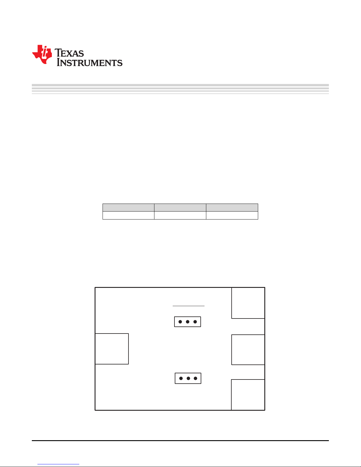
Figure 1 shows the connection points needed to fully and correctly interface with the TPS65980EVM.
Figure 1. Connection Points
4
TPS65980EVM SLVUA50–April 2014
Copyright © 2014, Texas Instruments Incorporated
Submit Documentation Feedback
Page 5

www.ti.com
The TPS65980 has three operating modes dictated by the voltage applied on TBT_IN. The total power
available at each of the outputs is determined by the operating mode. Table 2 summarizes the operating
modes in terms of input voltage range and output current ranges.
Operating Mode TBT_IN Vrange TBT_OUT Irange
Low Voltage 2.5V – 3.4V 5mA – 50mA Output Disabled Output Disabled
High Voltage 10V – 15.75V 235mA – 1A 0 – 1.44A
High Voltage
(Sleep)
(1)
Note: the total combined output current from TBT_OUT, CBL_OUT, and DEV_OUT should never
exceed 3.5A.
2.2 Jumper Settings
There are two digital input signals which can be set with jumpers as defined in Table 3. These signals
can be set to a logical value of “0” or “1” by moving the jumper between the 2 available positions (left and
right). See the TPS65980 data sheet for more information on the functionality of these signals.
Header Name Logic Jumper Position Effect
J5 DEV_EN 1 Left (TBT_OUT) DEV_OUT
J6 CBL_ILIM 1 Left (TBT_OUT) CBL_OUT using
Input/Output Supply Ranges
(1)
CBL_OUT DEV_OUT
(1)
Irange
(1)
5.2V – 15.75V 5mA – 31mA 0 – 235mA 0 – 700mA
Irange
0 – 2.5A
(1)
Digital Signal Jumpers
Disabled
DEV_EN 0 Right (GND) DEV_OUT Enabled
higher current limit
CBL_ILIM 0 Right (GND) CBL_OUT using
lower current limit
Setup
SLVUA50–April 2014 TPS65980EVM
Submit Documentation Feedback
5
Copyright © 2014, Texas Instruments Incorporated
Page 6

TBT
IN
+
-
J1
DEV_EN
J5
OFF|ON
CBL_ILIM
J6
HI|LOW
+
-
J2
+
-
J3
+
-
J4
DEV
OUT
TBT
OUT
CBL
OUT
3.0V – 3.319V
0mA – 700mA
3.221V – 3.319V
5mA – 31mA
3.171V – 3.319V
0mA – 235mA
5.2V – 15.75V
TBT
IN
+
-
J1
DEV_EN
J5
OFF|ON
CBL_ILIM
J6
HI|LOW
+
-
J2
+
-
J3
+
-
J4
DEV
OUT
TBT
OUT
CBL
OUT
OUTPUT
OFF
3.135V – 3.4V
5mA – 50mA
OUTPUT
OFF
2.5V – 3.4V
Setup
2.3 Device Configurations
Figure 2, Figure 3, Figure 4, and Figure 5illustrate the three operating modes discussed in section 2.1 as
well as the two programmable CBL_OUT current limits.
This is the average output voltage range for normal loads. During light load, the peak output voltage from TBT_OUT
may surpass 3.4V, but not exceeding 3.42V
www.ti.com
Figure 2. Low Voltage Input
This is the average output voltage range for normal loads. During light load, the average output voltage from
CBL_OUT may reach 3.4 with peaks not exceeding 3.42V.
6
TPS65980EVM SLVUA50–April 2014
Figure 3. High Voltage Input During Sleep
Copyright © 2014, Texas Instruments Incorporated
Submit Documentation Feedback
Page 7

TBT
IN
+
-
J1
DEV_EN
J5
OFF|ON
CBL_ILIM
J6
HI|LOW
+
-
J2
+
-
J3
+
-
J4
DEV
OUT
TBT
OUT
CBL
OUT
3.0V – 3.319V
0mA – 2500mA
3.221V – 3.319V
235mA – 1000mA
3.12V – 3.319V
0mA – 1440mA
TBT
IN
+
-
J1
DEV_EN
J5
OFF|ON
CBL_ILIM
J6
HI|LOW
+
-
J2
+
-
J3
+
-
J4
DEV
OUT
TBT
OUT
CBL
OUT
3.0V – 3.319V
0mA – 2500mA
3.221V – 3.319V
235mA – 1000mA
3.171V – 3.319V
0mA – 720mA
5.2V – 15.75V
www.ti.com
A This is the average output voltage range for normal loads. During light load, the average output voltage from
TBT_OUT and CBL_OUT may reach 3.4 with peaks not exceeding 3.42V
B The total combined output current from TBT_OUT, CBL_OUT, and DEV_OUT should never exceed 3.5A.
Figure 4. High Voltage Input With Lower CBL_OUT Current Limit
Setup
A This is the average output voltage range for normal loads. During light load, the average output voltage from
TBT_OUT and CBL_OUT may reach 3.4 with peaks not exceeding 3.42V
B The total combined output current from TBT_OUT, CBL_OUT, and DEV_OUT should never exceed 3.5A.
Figure 5. High Voltage Input With Higher CBL_OUT Current Limit
SLVUA50–April 2014 TPS65980EVM
Submit Documentation Feedback
Copyright © 2014, Texas Instruments Incorporated
7
Page 8

Setup
2.4 Test Points
Several test points are provided solely for the purpose measuring certain signals. It is NOT recommended
to use the test points to supply power to TBT_IN or load TBT_OUT, CBL_OUT, or DEV_OUT.
www.ti.com
Table 2. Test Point Descriptions
Test Point Signal Description
TP1 GND
TP2 DEV_OUT
TP3 Switching Node
TP4 BOOT
TP5 GND
TP6 TBT_IN
TP7 GND
TP8 TBT_OUT
TP9 Compensation Pin
TP10 GND
TP11 GND
TP12 Soft Start Pin
TP13 RESET_N Signal
TP14 HV_OK Signal
TP15 GND
TP16 CBL_OUT
8
TPS65980EVM SLVUA50–April 2014
Copyright © 2014, Texas Instruments Incorporated
Submit Documentation Feedback
Page 9

www.ti.com
3 Board Assembly and Layout
Figure 6 and Figure 7 show the top and bottom assembly for the TPS65980EVM.
Board Assembly and Layout
Figure 6. Top Layer Assembly
SLVUA50–April 2014 TPS65980EVM
Submit Documentation Feedback
Figure 7. Bottom Layer Assembly
9
Copyright © 2014, Texas Instruments Incorporated
Page 10

Board Assembly and Layout
Figure 8 and Figure 9 show the top and bottom layout for the TPS65980EVM.
www.ti.com
Figure 8. Top Layer Routing
10
TPS65980EVM SLVUA50–April 2014
Figure 9. Bottom Layer Routing
Copyright © 2014, Texas Instruments Incorporated
Submit Documentation Feedback
Page 11

www.ti.com
4 Schematic
The Schematic for the EVM is given in Figure 10.
Schematic
SLVUA50–April 2014 TPS65980EVM
Submit Documentation Feedback
Figure 10. Schematic
11
Copyright © 2014, Texas Instruments Incorporated
Page 12

Bill of Materials
www.ti.com
5 Bill of Materials
This section contains details on the bill of materials for the TPS65980EVM. Unpopulated items have a quantity of 0.
Bill of Materials
Designator Quantity Value Description Package Reference Part Number Manufacturer Alternate Part Alternate
Number Manufacturer
!PCB 1 Printed Circuit Board HVL071 Any
C1, C2, C8, C9 4 10µF CAP, CERM, 10µF, 25V, ±20%, X7R, 1210 1210 C3225X7R1E106M250AC TDK
C5, C15, C16 3 1µF CAP, CERM, 1µF, 10V, ±10%, X5R, 0603 0603 GRM188R61A105KA61D MuRata
C6, C12, C13 3 0.01µF CAP, CERM, 0.01µF, 25V, ±10%, X7R, 0402 0402 GRM155R71E103KA01D MuRata
C10 1 0.1µF CAP,CERM, 0.1µF, 25V, ±10%, X5R, 0402 0402 GRM155R61E104KA87D MuRata
D1, D2 2 Blue LED, Blue, SMD BLUE 0603 LED LB Q39G-L2N2-35-1 OSRAM
H9, H10, H11, 4 Bumpon, Hemisphere, 0.44 X 0.20, Clear Transparent Bumpon SJ-5303 (CLEAR) 3M
H12
J1, J2, J3, J4 4 C-282834-2 Header, Shrouded 2-pin, 100 mil space, 6.5x5.54 mm C-282834-2 Tyco
J5, J6 2 Header, TH, 100mil, 3x1, Gold plated, 230 mil above 3x1 Header TSW-103-07-G-S Samtec
insulator
L1 1 10µH Inductor, Shielded, Powdered Iron, 10µH, 6.8A, IHLP-4040DZ IHLP4040DZER100M01 Vishay-Dale
36.5Ω, SMD
Q1 1 25V MOSFET, N-CH, 25V, 4.5A, 2.28x.62x1.7mm 2.28x.62x1.7mm CSD86311W1723 Texas None
Instruments
R1, R2 2 249 RES, 249Ω, 1%, 0.063W, 0402 0402 CRCW0402249RFKED Vishay-Dale
R3 1 10.0kΩ RES, 10.0kΩ, 1%, 0.063W, 0402 0402 CRCW040210K0FKED Vishay-Dale
SH-J5, SH-J6 2 1x2 Shunt, 100mil, Gold plated, Black Shunt 969102-0000-DA 3M SNT-100-BK-G Samtec
TP1, TP5, TP7, 6 Black Test Point, Miniature, Black, TH Black Miniature Testpoint 5001 Keystone
TP10, TP11,
TP15
TP2, TP3, TP4, 10 Red Test Point, Compact, Red, TH RedCompact Testpoint 5005 Keystone
TP6, TP8, TP9,
TP12, TP13,
TP14, TP16
U1 1 Thunderbolt™ Bus Power Buck/Boost, RHF0024A RHF0024A TPS65980RHF Texas None
Instruments
C3, C7 0 10µF CAP, CERM, 10µF, 25V, ±20%, X7R, 1210 1210 C3225X7R1E106M250AC TDK
C4, C14 0 1µF CAP, CERM, 1µF, 10V, ±10%, X5R, 0805 0805 GRM219R61A105KC01D MuRata
C11 0 0.01µF CAP, CERM, 0.01µF, 25V, ±10%, X7R, 0402 0402 GRM155R71E103KA01D MuRata
FID1, FID2, 0 Fiducial mark. There is nothing to buy or mount. Fiducial N/A N/A
FID3
12
TPS65980EVM SLVUA50–April 2014
Submit Documentation Feedback
Copyright © 2014, Texas Instruments Incorporated
Page 13

IMPORTANT NOTICE
Texas Instruments Incorporated and its subsidiaries (TI) reserve the right to make corrections, enhancements, improvements and other
changes to its semiconductor products and services per JESD46, latest issue, and to discontinue any product or service per JESD48, latest
issue. Buyers should obtain the latest relevant information before placing orders and should verify that such information is current and
complete. All semiconductor products (also referred to herein as “components”) are sold subject to TI’s terms and conditions of sale
supplied at the time of order acknowledgment.
TI warrants performance of its components to the specifications applicable at the time of sale, in accordance with the warranty in TI’s terms
and conditions of sale of semiconductor products. Testing and other quality control techniques are used to the extent TI deems necessary
to support this warranty. Except where mandated by applicable law, testing of all parameters of each component is not necessarily
performed.
TI assumes no liability for applications assistance or the design of Buyers’ products. Buyers are responsible for their products and
applications using TI components. To minimize the risks associated with Buyers’ products and applications, Buyers should provide
adequate design and operating safeguards.
TI does not warrant or represent that any license, either express or implied, is granted under any patent right, copyright, mask work right, or
other intellectual property right relating to any combination, machine, or process in which TI components or services are used. Information
published by TI regarding third-party products or services does not constitute a license to use such products or services or a warranty or
endorsement thereof. Use of such information may require a license from a third party under the patents or other intellectual property of the
third party, or a license from TI under the patents or other intellectual property of TI.
Reproduction of significant portions of TI information in TI data books or data sheets is permissible only if reproduction is without alteration
and is accompanied by all associated warranties, conditions, limitations, and notices. TI is not responsible or liable for such altered
documentation. Information of third parties may be subject to additional restrictions.
Resale of TI components or services with statements different from or beyond the parameters stated by TI for that component or service
voids all express and any implied warranties for the associated TI component or service and is an unfair and deceptive business practice.
TI is not responsible or liable for any such statements.
Buyer acknowledges and agrees that it is solely responsible for compliance with all legal, regulatory and safety-related requirements
concerning its products, and any use of TI components in its applications, notwithstanding any applications-related information or support
that may be provided by TI. Buyer represents and agrees that it has all the necessary expertise to create and implement safeguards which
anticipate dangerous consequences of failures, monitor failures and their consequences, lessen the likelihood of failures that might cause
harm and take appropriate remedial actions. Buyer will fully indemnify TI and its representatives against any damages arising out of the use
of any TI components in safety-critical applications.
In some cases, TI components may be promoted specifically to facilitate safety-related applications. With such components, TI’s goal is to
help enable customers to design and create their own end-product solutions that meet applicable functional safety standards and
requirements. Nonetheless, such components are subject to these terms.
No TI components are authorized for use in FDA Class III (or similar life-critical medical equipment) unless authorized officers of the parties
have executed a special agreement specifically governing such use.
Only those TI components which TI has specifically designated as military grade or “enhanced plastic” are designed and intended for use in
military/aerospace applications or environments. Buyer acknowledges and agrees that any military or aerospace use of TI components
which have not been so designated is solely at the Buyer's risk, and that Buyer is solely responsible for compliance with all legal and
regulatory requirements in connection with such use.
TI has specifically designated certain components as meeting ISO/TS16949 requirements, mainly for automotive use. In any case of use of
non-designated products, TI will not be responsible for any failure to meet ISO/TS16949.
Products Applications
Audio www.ti.com/audio Automotive and Transportation www.ti.com/automotive
Amplifiers amplifier.ti.com Communications and Telecom www.ti.com/communications
Data Converters dataconverter.ti.com Computers and Peripherals www.ti.com/computers
DLP® Products www.dlp.com Consumer Electronics www.ti.com/consumer-apps
DSP dsp.ti.com Energy and Lighting www.ti.com/energy
Clocks and Timers www.ti.com/clocks Industrial www.ti.com/industrial
Interface interface.ti.com Medical www.ti.com/medical
Logic logic.ti.com Security www.ti.com/security
Power Mgmt power.ti.com Space, Avionics and Defense www.ti.com/space-avionics-defense
Microcontrollers microcontroller.ti.com Video and Imaging www.ti.com/video
RFID www.ti-rfid.com
OMAP Applications Processors www.ti.com/omap TI E2E Community e2e.ti.com
Wireless Connectivity www.ti.com/wirelessconnectivity
Mailing Address: Texas Instruments, Post Office Box 655303, Dallas, Texas 75265
Copyright © 2014, Texas Instruments Incorporated
 Loading...