

Page 1

Abstract
This user’s guide provides a detailed account of the TPS65912x Evaluation Module (EVM) including a
general overview, schematic diagram, board layout, setup instructions, graphical user interface (GUI) and
bill of materials (BOM). Use this EVM for integrated circuit (IC) evaluation and also for design reference.
The TPS65912x is a power management unit (PMU) for processor power.
How to Use This Manual
This document is formatted in order of operation; become familiar with the schematic and layout before
proceeding to the setup section.
Notational Conventions
• EVM – Evaluation Module
• PMU – Power Management Unit
• IC – Integrated Circuit
• PMIC – Power Management Integrated Circuit
• BOM – Bill of Materials
• PCB – Printed-circuit board
• GUI – Graphical User Interface
Preface
SLVU750A–July 2012–Revised May 2013
TPS65912xEVM-081 User's Guide
Information About Cautions and Warnings
This book may contain cautions and warnings.
Please read this document thoroughly.
Not following this document in detail could potentially damage your software or
equipment.
Please take all possible safety precautions.
Improper use of this evaluation module could potentially cause
physical harm.
The information in a caution or a warning is provided for protection. Please read each caution and warning
carefully.
CAUTION
WARNING
SLVU750A–July 2012–Revised May 2013 TPS65912xEVM-081 User's Guide
Submit Documentation Feedback
Copyright © 2012–2013, Texas Instruments Incorporated
1
Page 2

Related Documentation From Texas Instruments
Related Documentation From Texas Instruments
Refer to the data sheet, SWCS054, for detailed information on the TPS65912x IC features and operating
specifications.
If You Need Assistance
Visit the TI E2E Forums: http://e2e.ti.com
FCC Warning
This equipment is intended for use in a laboratory test environment only. It generates, uses, and can
radiate radio frequency energy and has not been tested for compliance with the limits of computing
devices pursuant to subpart J of part 15 of FCC rules, which are designed to provide reasonable
protection against radio frequency interference. Operation of this equipment in other environments may
cause interference with radio communications, in which case the user, at his/her own expense, is required
to take whatever measures necessary to correct this interference.
www.ti.com
2
TPS65912xEVM-081 User's Guide SLVU750A–July 2012–Revised May 2013
Copyright © 2012–2013, Texas Instruments Incorporated
Submit Documentation Feedback
Page 3

1 TPS65912xEVM-081 Overview
The TPS65912xEVM-081 allows evaluation of the IC and serves a reference design.
1.1 Introduction to Using the TPS65912xEVM-081
Make a copy of this user’s guide available to the operator of this EVM.
User's Guide
SLVU750A–July 2012–Revised May 2013
TPS65912xEVM-081
SLVU750A–July 2012–Revised May 2013 TPS65912xEVM-081
Submit Documentation Feedback
Copyright © 2012–2013, Texas Instruments Incorporated
3
Page 4
CLOCKS
Components with no values are not installed.
1
DEF_SPI_I2C
GPIO1_MISO
GPIO2_CE
LEDA_GPIO3
LEDB_GPIO4
LEDC_GPIO5
GND
A1
VLDO7
A2
VINLDO67
A3
VLDO6
A4
VDCDC4
A5
PGND4
A6
SW4
A7
VINDCDC4
A8
LSO
A9
LSO
B1
LEDC_GPIO5
B2
LEDB_GPIO4
B3
LEDA_GPIO3
B4
VDCDC4_GND
B5
PGND4
B6
SW4
B7
VINDCDC4
B8
LSI
B9
LSI
C1
VINDCDC3
C2
EN_LS1
C3
EN_LS0
C4
GPIO2_CE
C5
EN4_DCDC4_SEL
C6
EN3_DCDC3_SEL
C7
AGND
C8
VINDCDC_ANA
C9
VINDCDC2
D1
SW3
D2
CONFIG2
D3
PWRON
D4
GPIO1_MISO
D5
SCLK_SCK
D6
POWERHOLD_ON
D7
VDCDC2
D8
EN2_DCDC2_SEL
D9
SW2
E1
PGND3
E2
CONFIG1
E3
DGND
E4
SDA_MOSI
E5
SCL_AVS_CLK_REQ1
E6
SDA_AVS_CLK_REQ2
E7
DEF_SPI_I2C-GPIO0
E8
EN1_DCDC1_SEL
E9
PGND2
F1
VINLDO4
F2
VDCDC3
F3
AGND
F4
VCON_PWM
F5
VCON_CLK
F6
OMAP_WDI_32K_OUT
F7
VDDIO
F8
VINLDO3
F9
VLDO3
G1
VLDO4
G2
VCCS_VIN_MON
G3
LDOAO
G4
SLEEP_PWR_REQ
G5
INT1
G6
~RESPWRON_VSUP_OUT
G7
CPCAP_WDI
G8
VINLDO5
G9
VLDO5
H1
VLD02
H2
VCC
H3
VREF1V25
H4
VDCDC1_GND
H5
PGND1
H6
SW1
H7
VINDCDC1
H8
VINLDO8
H9
VLDO8
J1
VLDO10
J2
VINLDO1210
J3
VLDO1
J4
VDCDC1
J5
PGND1
J6
SW1
J7
VINDCDC1
J8
VINLDO9
J9
VLDO9
U1
TPS65912YFF
L3 1.0uH
L4 1.0uH
C1 22uF
C2
10uF
C3
10uF
L1 1.0uH
C5
10uF
C6
10uF
C7 10uF
C8
10uF
C9 10uF
L2 1.0uH
C10
10uF
C11
2.2uF
C12 2.2uF
C13 2.2uF
C14 2.2uF
C15 2.2uF
C16 2.2uF
C17 2.2uF
C18 2.2uF
C19 2.2uF
C20 2.2uF
C21 2.2uF
C22 2.2uF
C23 2.2uF
C24 4.7uF
C25 4.7uF
C26 4.7uF
C27 4.7uF
D1
LTST-C190YKT
D2
LTST-C190GKT
D3
LTST-C190CKT
C28 220nF
C29 2.2uF
C30
2.2uF
R1 0
R13 0
C4 22uF
C31 2.2uF
1
2
3
4
5
6
7
J40
R9
R10
R11
3.30k
R12
R14
3.30k
R15
3.30k
Y1
R19
J1
1
2
3
4 5
6
7
8
U2
Y2
R2
R3
J2
R16
0
R5
0
R6
0
R7 0
R17
0
C53
J8
R8
R20 0
R21
0
R22 0
R24
0
VDCDC4
VDCDC1
VDCDC4_SENSE
VDCDC4_GND_SENSE
VDCDC3
VDCDC2
LSI
LSO
VINLDO3
VLDO3
VINLDO1210
VLDO1
VLDO2
VINLDO4
VLDO4
VINLDO5
VLDO5
VINLDO67
VLDO6
VLDO7
VINLDO8
VLDO8
VINLDO9
VLDO9
VLDO10
VCC
SCL_CLK
SDA_MOSI
GPIO1_MISO
GPIO2_CE
SCL_AVS
SDA_AVS
EN2_DCDC2
EN3_DCDC3
EN4_DCDC4
PWRHOLD
VBAT
VBAT
LDOAO
VREF1V25
LEDA_GPIO3
LEDB_GPIO4
LEDC_GPIO5
VBAT
CONFIG1
CONFIG2
CPCAP_WDI
DEF_SPI_I2C
EN1_DCDC1
EN_LS0
EN_LS1
INT1
NRESPWRON
OMAP_WDI
PWRON
SLEEP
VCCS_VIN_MON
VCON_CLK
VCON_PWM
VDCDC1_GND_SENSE
VDCDC1_SENSE
VDDIO
VDCDC3_SENSE
VDCDC2_SENSE
VBAT
VBAT
VBAT
VBAT
VDDIO
DEF_SPI_I2C
GPIO1_MISO
GPIO2_CE
LEDA_GPIO3
LEDB_GPIO4
LEDC_GPIO5
GND
TXCOUT
SCL_CLK
SDA_MOSI
INTA
INTA
INTA
SQW_INTB
VLDO3
VCLKS
GND
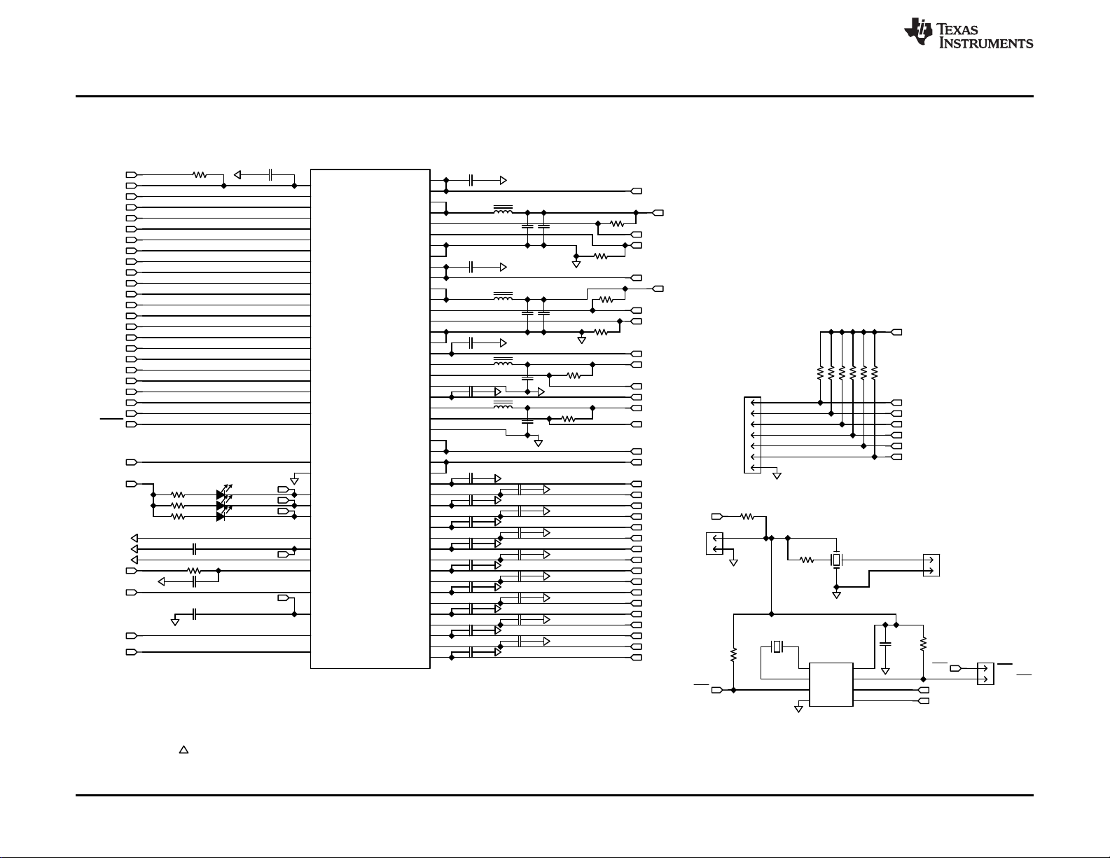
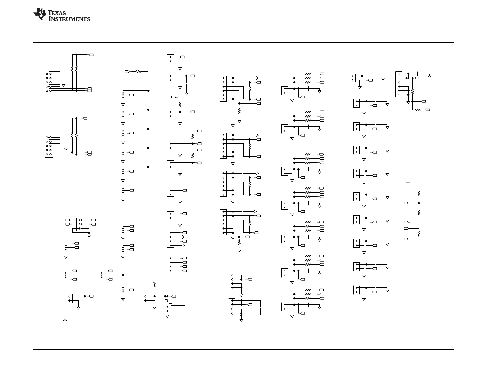
Schematic Diagram
2 Schematic Diagram
The following figures represent the schematic diagram for the EVM:
www.ti.com
4
TPS65912xEVM-081 SLVU750A–July 2012–Revised May 2013
Figure 1. TPS65912xEVM-081 Schematic Page 1/2
Submit Documentation Feedback
Copyright © 2012–2013, Texas Instruments Incorporated
Page 5
SPI
ENABLE
CONFIG
I2C
AVS-I2C
DCDC OUTPUT
LOAD SWITCH
VDCDC1
VDCDC2
VDCDC3
VDCDC4
LSI
LSO
LDO SUPPLY
VINLDO1210
VINLDO3
VINLDO4
VINLDO5
VINLDO67
VINLDO8
VINLDO9
LDO OUTPUT
VLDO1
VLDO2
VLDO3
VLDO4
VLDO5
VLDO6
VLDO7
VLDO8
VLDO9
VLDO10
SUPPLY INPUT
CLK_REQ1
CLK_REQ2
PWR_REQ
3V to 5V
GND
GND
GND
GND
GND
GND
GND
GND
GND
GND
GND
GND
GND
GND
GND
GND
GND
GND
GND
GND
GND
GND
GND
S+
S-
S+
S+
S+
S-
VREF1V25
GND
VDDIO
GND
SLEEP
GND
INT1
GND
NRESPWRON
GND
SCL_AVS
GND
SDA_AVS
GND
VCON_CLK
GND
VCON_PWM
GND
CPCAP_WDI
LDOAO
OMAP_WDI
VDDIO
EN_LS1
GND
VDDIO
EN_LS0
GND
VDDIO
EN4
GND
VDDIO
EN3
GND
VDDIO
EN2
GND
VDDIO
EN1
GND
LDOA0
CONFIG1
GND
LDOA0
CONFIG2
GND
LDOA0
DEF_SPI_I2C
GND
LSI
VCCS_VIN_MON
VBAT
VCCS_VIN_MON
GND
LDOA0
PWRON
VDDIO
(JP12)
PWRHOLD
GND
PWRON
GND
Components with no values are not installed.
1
VDDIO
VBAT
GND
PWRHOLD
JP8
JP9
JP1
JP2
JP3
JP4
JP5
1
2
J28
1
2
3
4
J29
JP6
JP7
1
2
J30
1
2
J31
1
2
J35
1
2
J36
1
2
3
4
5
6
7
8
9
10
J37
1
2
3
4
5
6
7
8
9
10
J38
1
2
3 4
5
6
J39
1
2
3
4
J32
R30
3.30k
R31
3.30k
R32
3.30k
R33
3.30k
1
2
J34
1
2
3
4
5
6
J3
C32 10uF
R26
0
R27
0
1
2
3
4
5
6
J4
C33 10uF
R28
0
1
2
3
4
5
6
J5
C34 10uF
R29
0
1
2
3
4
5
6
J6
C35 10uF
R34
0
R35
0
1
2
3
4
J26
1
2
3
4
J27
1
2
J9
1
2
J10
1
2
J11
1
2
J12
C36 2.2uF
C37 2.2uF
C38 2.2uF
C39 2.2uF
R36
R37 0
R38
R39
R40
R41 0
R42
R43 0
R44
R45 0
1
2
J13
C40 2.2uF
R46
R47 0
1
2
J14
C41 2.2uF
R48
R49 0
1
2
J15
C42 2.2uF
R50
R51 0
1
2
J16
C43
2.2uF
1
2
J17
C44
2.2uF
1
2
J18
C45
2.2uF
1
2
J19
C46
2.2uF
1
2
J20
C47
2.2uF
1
2
J21
C48
2.2uF
1
2
J22
C49
2.2uF
1
2
J23
C50
2.2uF
1
2
J24
C51
2.2uF
1
2
J25
C52
2.2uF
1
2
3
4
5
6
J7
C54 10uF
R53
0
R54
R56
R57
R58
0
JP11
S1
R18
10.0k
1
2
J33
C55
4.7uF
R23
3.30k
1
2
J41
1
2
J42
R60
R61
C56
22uF
R4 0
JP10
R25
R52
R55
R59
R62
JP12
LDOAO
LDOAO
LDOAO
CONFIG1
CONFIG2
DEF_SPI_I2C
EN1_DCDC1
EN2_DCDC2
EN3_DCDC3
EN4_DCDC4
CPCAP_WDI
NRESPWRON
LDOAO
EN_LS0
EN_LS1
VREF1V25
VDDIO
SLEEP
INT1
SDA_MOSI
SCL_CLK
SDA_AVS
GPIO2_CE
SDA_MOSI SCL_CLK
GPIO1_MISO
VDDIO
OMAP_WDI
VDDIO
VCON_CLK
VCON_PWM
VDDIO
VDDIO
SCL_AVS
VCCS_VIN_MON
VBAT
LSI
VDCDC1
VDCDC1_SENSE
VDCDC1_GND_SENSE
VDCDC2
VDCDC2_SENSE
VDCDC3
VDCDC3_SENSE
VDCDC4
VDCDC4_SENSE
VDCDC4_GND_SENSE
LSI
LSO
VINLDO1210
VINLDO3
VINLDO4
VINLDO5
VDCDC3
VBAT
VDCDC2
VDCDC3
VDCDC2
VBAT
VDCDC2
VBAT
VDCDC3
VBAT
VINLDO67
VDCDC3
VBAT
VINLDO8
VDCDC3
VBAT
VINLDO9
VDCDC3
VBAT
VLDO1
VLDO2
VLDO3
VLDO4
VLDO5
VLDO6
VLDO7
VLDO8
VLDO9
VLDO10
VBAT
LSI
VBAT
LSI
LSO
VBAT
VDCDC2
LDOAO
VDDIO
PWRHOLD
PWRON
SCL_AVS
SDA_AVS
VDDIO
VDDIO
VDDIO
VCC
VDCDC2
VDCDC2
VDCDC2
VDCDC2
VDCDC3
www.ti.com
Schematic Diagram
SLVU750A–July 2012–Revised May 2013 TPS65912xEVM-081
Submit Documentation Feedback
Figure 2. TPS65912xEVM-081 Schematic Page 2/2
Copyright © 2012–2013, Texas Instruments Incorporated
5
Page 6

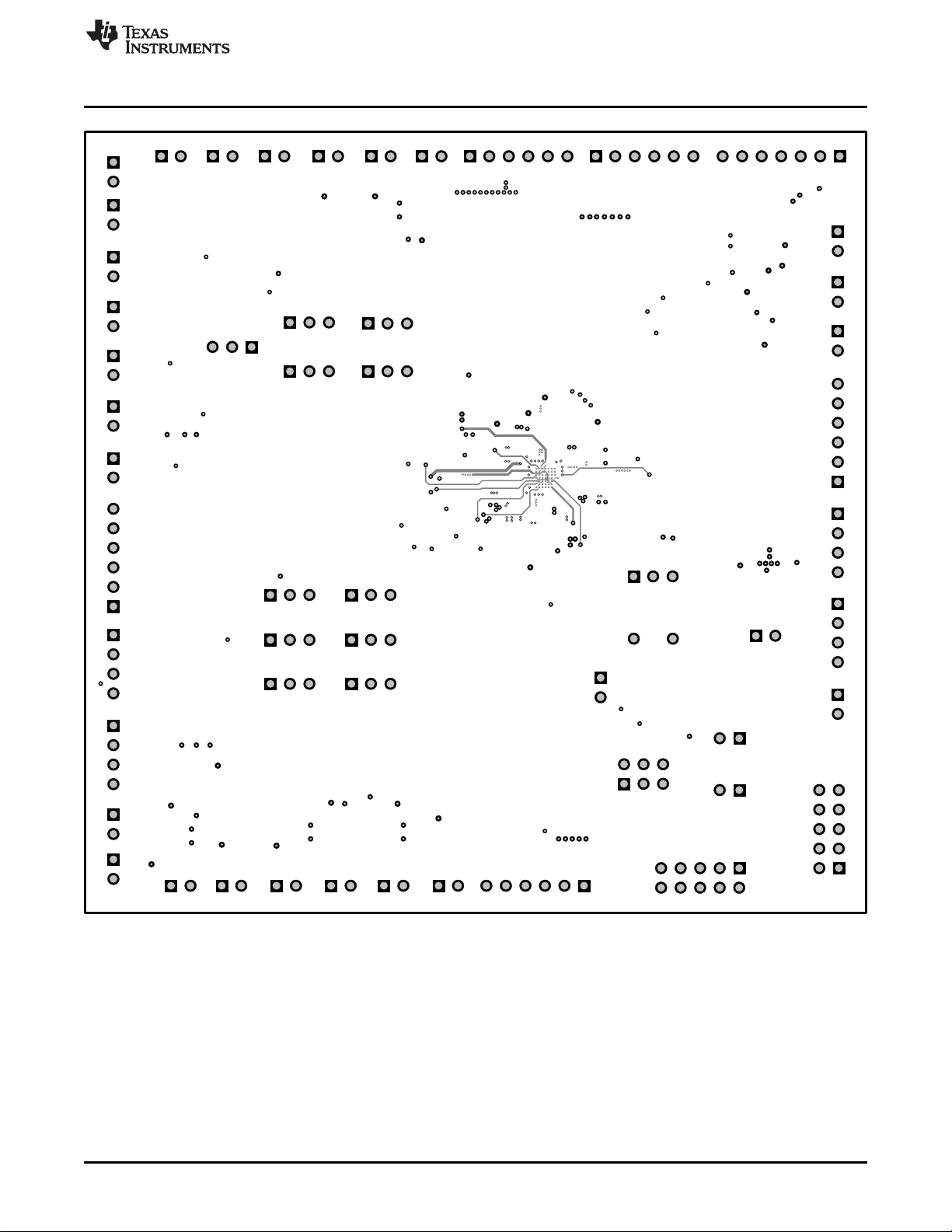
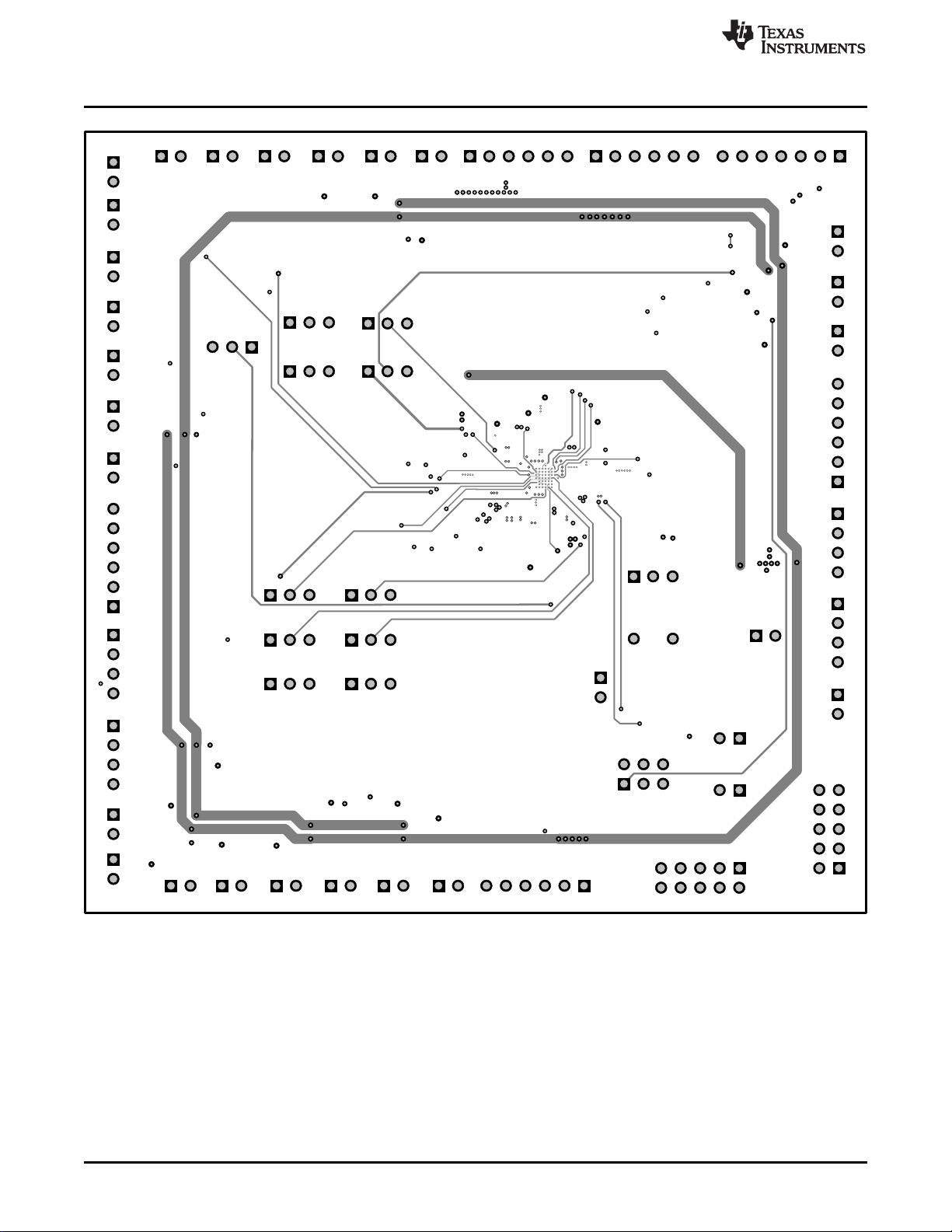
Layout
3 Layout
The EVM board layout is detailed in the following images:
www.ti.com
Figure 3. TPS65912xEVM-081 Layout Top
6
TPS65912xEVM-081 SLVU750A–July 2012–Revised May 2013
Copyright © 2012–2013, Texas Instruments Incorporated
Submit Documentation Feedback
Page 7
www.ti.com
Layout
Figure 4. TPS65912xEVM-081 Layout Layer 2
SLVU750A–July 2012–Revised May 2013 TPS65912xEVM-081
Submit Documentation Feedback
Copyright © 2012–2013, Texas Instruments Incorporated
7
Page 8
Layout
www.ti.com
Figure 5. TPS65912xEVM-081 Layout Layer 3
8
TPS65912xEVM-081 SLVU750A–July 2012–Revised May 2013
Copyright © 2012–2013, Texas Instruments Incorporated
Submit Documentation Feedback
Page 9

www.ti.com
Layout
Figure 6. TPS65912xEVM-081 Layout Layer 4
SLVU750A–July 2012–Revised May 2013 TPS65912xEVM-081
Submit Documentation Feedback
Copyright © 2012–2013, Texas Instruments Incorporated
9
Page 10

Layout
www.ti.com
10
Figure 7. TPS65912xEVM-081 Layout Layer 5
TPS65912xEVM-081 SLVU750A–July 2012–Revised May 2013
Copyright © 2012–2013, Texas Instruments Incorporated
Submit Documentation Feedback
Page 11

www.ti.com
Layout
Figure 8. TPS65912xEVM-081 Layout Bottom
SLVU750A–July 2012–Revised May 2013 TPS65912xEVM-081
Submit Documentation Feedback
Copyright © 2012–2013, Texas Instruments Incorporated
11
Page 12

Setup
4 Setup
This section describes setup of the EVM.
4.1 Additional Hardware
Two external power supplies are required to operate the EVM. One supply must deliver 5 A at 5 V and the
other must deliver 1 A at 1.8 V.
NOTE: I2C™ Bus: A personal computer and USB-TO-GPIO box and cable are required to use the
I2C bus with the GUI.
4.2 Jumper Settings
Verify shorting jumpers are installed per Table 1:
www.ti.com
Table 1. Jumper Settings
Jumper Shunt Location
JP1 Between pin1 and pin2
JP2 Between pin2 and pin3
JP3 Between pin2 and pin3
JP4 Between pin2 and pin3
JP5 Between pin2 and pin3
JP6 Between pin2 and pin3
JP7 Between pin2 and pin3
JP8 Between pin2 and pin3
JP9 Between pin2 and pin3
JP10 Between pin2 and pin3
JP11 Between pin1 and pin2
4.3 Power Supply Connections
Set the 5-V power supply to the off state and connect it to the VBAT input header, J9; positive lead to pin
1 and negative lead to pin 6.
Make sure the 1.8-V power supply is switched off and connect it to the VDDIO input header, J43; positive
lead to pin 1 and negative lead to pin 2.
Switch on the 1.8-V power supply.
Switch on the 5-V power supply.
Neither supply sources more than a few milliamps in this no load condition.
4.4 Operation
If the preceding instructions were followed, the EVM is operating under its default conditions. Refer to the
TPS65912x data sheet (SWCS054) for default converter/LDO state and loading conditions.
12
TPS65912xEVM-081 SLVU750A–July 2012–Revised May 2013
Copyright © 2012–2013, Texas Instruments Incorporated
Submit Documentation Feedback
Page 13
www.ti.com
5 Layout Considerations
This section describes basic layout requirements for the TPS65912x.
5.1 General Layout
As for all switching power supplies, the layout is an important step in the design. Proper function of the
device demands careful attention to PCB layout. Follow board layout instructions carefully to attain the
specified performance. If the layout is not carefully done, the regulators may show poor line and/or load
regulation and stability issues as well as EMI problems. It is critical to provide a low impedance ground
path. Therefore, use wide and short traces for the main current paths. Place input capacitors as close as
possible to the IC pins as well as the inductor and output capacitor. Keep the common path to the GND
pins, which returns the small signal components, and the high current of the output capacitors as short as
possible to avoid ground noise. Connect the VDCDCx trace right to the output capacitor and routed away
from noisy components and traces (for example, the L1, L2, L3 and L4 traces).
5.2 Critical Signals for Layout
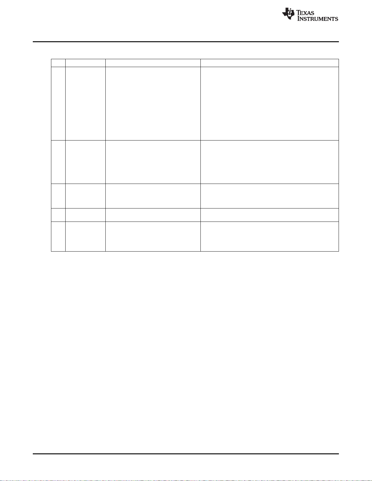
As outlined above, a number of signals require careful layout. Item numbers are assigned in Table 2
linking them to the examples in Section 5.3.
Item Signal Name Description Layout Guidelines
1 PGND1, Power-ground connection for DCDC1 to Connect to the GND plane. Ideally, route this signal on the
PGND2, DCDC4. This pin is internally tied to the same layer that the device is placed. Use multiple vias to the
PGND3, PGND4 source of the low side transistor and GND plane if it is on a different layer. As DCDC1 and DCDC4
carries the full output current + inductor are designed (operated) for larger output current, they are
current ripple. more critical than DCDC2 and DCDC3. The GND-terminal of
2 VINDCDC1, Input supply to the power stage for Connect to the supply voltage trace. Place an input capacitor
VINDCDC2,VIN DCDC1 to DCDC4. This pin is connected on each of the VINDCDCx pins with low impedance to GND
DCDC3, to the high-side power switch and carries and low impedance to the VINDCDCx pin. The input capacitor
VINDCDC4 the full output current + inductor current will have to buffer the input current rising within less than
ripple. As there is only an input current 10ns to the average output current (in PWM mode) minus the
when the internal high-side switch is inductor current ripple.
closed, the input current of a step-down
converter is discontinuous. This causes
current spikes on the input and requires
an input capacitor on each of the
VINDCDCx pins.
3 VINDCD-ANA Analog supply input to the DCDC1-to- This pin needs to be powered by the same voltage
DCDC4 converters. It supplies part of the VINDCDC1 to VINDCDC4 are tied to. Its input should be
gate driver and other analog circuitry. properly bypassed with a capacitor and routed to the supply
Layout Considerations
Table 2. Layout Guidelines and Descriptions
the output capacitor requires a low-impedance connection to
the respective PGND pin, as in case where the internal lowside switch is closed, the current flows in the path of output
inductor, output capacitor, PGND pin and L pin. Do not
connect VDCDCx_GND (the GND-SENSE connection for
DCDC1 and DCDC4) directly to the PGND pins. Tie
VDCDCx_GND to the GND-pad of the output capacitor or
directly to the GND plane. Tie AGND directly to the GND
plane. Connect PGND to the GND-plane independently of
other pins, not coupling noise on PGND into other pins.
voltage separately from VINDCDCx in order to avoid noise
generated by the power stages being coupled into
VINDCDC_ANA. Its input current is only a few mA, so the
trace does not have to be very wide.
SLVU750A–July 2012–Revised May 2013 TPS65912xEVM-081
Submit Documentation Feedback
Copyright © 2012–2013, Texas Instruments Incorporated
13
Page 14
Layout Considerations
Item Signal Name Description Layout Guidelines
4 L1, L2, L3, L4 These are the connections to the mid The pin carries the output current including inductor current
5 VDCDC1, Voltage feedback pins for DCDC1 to The pins are high impedance (MR) and sensible to noise from
VDCDC2, DCDC4 the switch node. The trace should not be routed in parallel to
DCDC3,VDCDC the L-traces and should be tied to the V+-pad of the output
4 capacitor directly.
6 VDCDC1_GND, GND-terminal for remote sense The pins are the GND connections for remote sense and can
VDCDC4_GND either be tied to the GND pad of the output capacitor or
7 Vcc Analog supply voltage pin Must be bypassed with a separate input capacitor, does not
8 AGND, DGND Analog and digital GND connection These GND pins need to be tied to the GND plane. The
www.ti.com
Table 2. Layout Guidelines and Descriptions (continued)
point of the power stage consisting of the ripple. It charges the output capacitor through the high side
high- and low-side switch. The output switch and inductor from the input supply and through the
inductor is connected here. inductor and GND while the high side switch is open and low
side switch is closed. As the L pins toggle with the switching
frequency with high slew rates the trace should be routed
apart from sensitive signals such as the feedback connection
to the error amplifier (VDCDCx pins). It is acceptable to
increase the trace length in order to place the input capacitor
close to the device. Having the input capacitor close to
TPS65912x is more critical than having a short connection to
the output inductor as long as the L-trace is shielded to the
feedback trace.
DCDC1 and DCDC4 allow remote sense, so the pin could
alternatively be routed to the input capacitor on the load side.
Coupling from fast switching signals must be avoided.
simply to the GND plane. DO NOT CONNECT TO PGND
PINS DIRECTLY.
carry high currents.
current is quite small but they are the GND connection of the
analog and digital circuitry such as the control loop, so the
connection to a solid GND plane needs to be done without
using long traces- preferably by a via to the GND plane.
14
TPS65912xEVM-081 SLVU750A–July 2012–Revised May 2013
Copyright © 2012–2013, Texas Instruments Incorporated
Submit Documentation Feedback
Page 15

www.ti.com
5.3 Detailed Layout Example
Note that the top view is shown here for the device, while the data sheet of TPS65912 shows its pinout as
bottom view.
5.3.1 Connection to Power GND
Layout Considerations
Figure 9. Example for Item1: GND Connections for Elements in DCDC1.
Figure 10. Example for Item 1. GND Plane
SLVU750A–July 2012–Revised May 2013 TPS65912xEVM-081
Submit Documentation Feedback
Copyright © 2012–2013, Texas Instruments Incorporated
15
Page 16

Layout Considerations
5.3.2 Input Capacitor
www.ti.com
Figure 11. Example for Item 2: GND Connections for Elements in DCDC1.
5.3.3 Analog Supply
16
Figure 12. Example for Item 3: Analog Supply
TPS65912xEVM-081 SLVU750A–July 2012–Revised May 2013
Copyright © 2012–2013, Texas Instruments Incorporated
Submit Documentation Feedback
Page 17

www.ti.com
5.3.4 Inductor
Layout Considerations
Figure 13. Example for Item 4: Inductor Location and Routing
SLVU750A–July 2012–Revised May 2013 TPS65912xEVM-081
Submit Documentation Feedback
Copyright © 2012–2013, Texas Instruments Incorporated
17
Page 18

Layout Considerations
5.3.5 DCDC Output Voltage Feedback and Remote Sensing
www.ti.com
18
Figure 14. Example for Items 5 and 6: DCDC Feedback and Remote Sensing
TPS65912xEVM-081 SLVU750A–July 2012–Revised May 2013
Copyright © 2012–2013, Texas Instruments Incorporated
Submit Documentation Feedback
Page 19

www.ti.com
5.3.6 Analog Supply Voltage Pin
Layout Considerations
Figure 15. Example for Item 7: Vcc, Analog Supply Voltage
5.3.7 Analog, Digital and Power GND Connections
Figure 16. Example for Item 8: Connection of PGND to GND
SLVU750A–July 2012–Revised May 2013 TPS65912xEVM-081
Submit Documentation Feedback
Copyright © 2012–2013, Texas Instruments Incorporated
19
Page 20

Layout Considerations
www.ti.com
20
Figure 17. Example for Item 8: Connection of AGND and DGND to GND
TPS65912xEVM-081 SLVU750A–July 2012–Revised May 2013
Copyright © 2012–2013, Texas Instruments Incorporated
Submit Documentation Feedback
Page 21

www.ti.com
6 Graphical User Interface
The provided GUI facilitates PC to IC communication though the I2C bus using the USB-TO-GPIO box and
USB cable. Please refer to USB Interface Adapter Evaluation Module User's Guide, SLLU093, for detailed
operating instructions of the USB-TO-GPIO interface. Connect the 10-pin ribbon cable to J60 of the EVM.
Connect the USB cable of the USB-TO-GPIO to the PC. An overview of the GUI is shown in Figure 18.
Graphical User Interface
Figure 18. Graphical User Interface Screen Shot
SLVU750A–July 2012–Revised May 2013 TPS65912xEVM-081
Submit Documentation Feedback
Copyright © 2012–2013, Texas Instruments Incorporated
21
Page 22

Bill of Materials
7 Bill of Materials
Table 3. PWR081A BOM
Count
-001 -002 RefDes Value Description Size Part Number MFR
3 3 C1, C4, C56 22 µF Capacitor, ceramic, 6.3 V, X5R, 20% 0805 GRM21BR60J226ME39 Murata
33 33 C16-23, C29-31, C11-14, 2.2 µF Capacitor, ceramic, 10 V, X7R, 10% 0603 GRM188R71A225KE15 Murata
C36-52, C15
13 13 C2-3, C5-10, C32-35, C54 10 µF Capacitor, ceramic, 6.3 V, X5R, 20% 0603 GRM188R60J106ME47 Murata
5 5 C24-27, C55 4.7 µF Capacitor, ceramic, 6.3 V, X5R, 10% 0603 GRM188R60J475KE19 Murata
1 1 C28 220 nF Capacitor, ceramic, 6.3 V, X5R, 20% 0603 std std
0 0 C53 Open Capacitor, ceramic, 10 V, X5, 20% 0603 STD STD
1 1 D1 LTST-C190YKT Diode, LED, yellow, 2.1 V, 20 mA, 6 mcd 0603 LTST-C190YKT Lite On
1 1 D2 LTST-C190GKT Diode, LED, green, 2.1 V, 20 mA, 6 mcd 0603 LTST-C190GKT Lite On
1 1 D3 LTST-C190CKT Diode, LED, red, 2.1 V, 20 mA, 6 mcd 0603 LTST-C190CKT Lite On
0 0 J1-2, J8 Open Header, male 2-pin, 100-mil spacing 0.100 in × 2 PEC02SAAN Sullins
4 4 J26-27, J29, J32 PEC04SAAN Header, male 4-pin, 100-mil spacing 0.100 in × 4 PEC04SAAN Sullins
5 5 J3-7 PEC06SAAN Header, male 6-pin, 100-mil spacing 0.100 in × 6 PEC06SAAN Sullins
2 2 J37-38 N2510-6002RB Connector, male straight 2 × 5 pin, 100-mil spacing, 4 wall 0.338 × 0.788 in N2510-6002RB 3M
1 1 J39 30306-6002HB Connector, male right angle 2 × 3 pin, 100-mil spacing, 0.100 in × 2X3 30306-6002HB 3M
shrouded
1 1 J40 PEC07SAAN Header, male 7-pin, 100-mil spacing 0.100 in × 7 PEC07SAAN Sullins
26 26 J9-25, J28, J30-31, J33-36, PEC02SAAN Header, male 2-pin, 100-mil spacing 0.100 in × 2 PEC02SAAN Sullins
J41-42
12 12 JP1-12 PEC03SAAN Header, male 3-pin, 100-mil spacing 0.100 in × 3 PEC03SAAN Sullins
4 4 L1-4 1.0 µH Inductor, SMT ±30% 2 × 2.5 mm 1239AS-H-1R0N=P2 Toko
24 24 R1, R4-7, R13, R16-17, 0 Ω Resistor, chip, 1/16W, 1% 0603 STD STD
R20-22, R24, R26-29, R3435, R37, R40, R45, R47,
R49, R51
8 8 R14, R31-32, R15, R33, 3.30 kΩ Resistor, chip, 1/16W, 1% 0603 STD STD
R11, R23, R30
1 1 R18 10.0 kΩ Resistor, chip, 1/16W, 1% 0603 STD STD
0 0 R19, R8, R2-3 Open Resistor, chip, 1/16W, 1% 0603 std std
1 1 R53 0 Ω Resistor, chip, 1/10W, ±1% 0805 STD STD
0 0 R54 open Resistor, chip, 1/10W, ±1% 0805 STD STD
0 0 R56-57 open Resistor, metal film, 1/4W, ± 1% 1206 STD Vishay
1 1 R58 0 Ω Resistor, metal film, 1/4W, ± 1% 1206 STD Vishay
20 20 R9-10, R36, R12, R38-39, open Resistor, chip, 1/16W, 1% 0603 STD STD
R41-44, R46, R48, R25,
R50, R52, R55, R59-62
1 1 S1 KT11P2JM34LFS Switch, SPST, PB momentary, sealed tactile 0.245 × 0.251 in KT11P2JM34LFS C & K
www.ti.com
22
TPS65912xEVM-081 SLVU750A–July 2012–Revised May 2013
Submit Documentation Feedback
Copyright © 2012–2013, Texas Instruments Incorporated
Page 23

www.ti.com
Table 3. PWR081A BOM (continued)
Count
-001 -002 RefDes Value Description Size Part Number MFR
1 0 U1 TPS659121YFF IC, PMU FOR PROCESSOR POWER BGA TPS659121YFF TI
0 1 U1 TPS659122YFF IC, PMU FOR PROCESSOR POWER BGA TPS659122YFF TI
0 0 U2 Open IC, REAL-TIME CLOCK WITH I2C SERIAL INTERFACE SO IDT1337DCGI IDT
0 0 Y1 Open Oscillator, SMT, xxMHz, ±3ppm per year 3.2 × 5 mm CXO-7CxxMHz TXC
0 0 Y2 Open Clock oscillator HC-49 MPxxx CTS
12 12 – – Shunt, 100-mil, black 0.100 929950-00 3M
1 1 – – PCB PWR081 Any
Bill of Materials
SLVU750A–July 2012–Revised May 2013 TPS65912xEVM-081
Submit Documentation Feedback
Copyright © 2012–2013, Texas Instruments Incorporated
23
Page 24

IMPORTANT NOTICE
Texas Instruments Incorporated and its subsidiaries (TI) reserve the right to make corrections, enhancements, improvements and other
changes to its semiconductor products and services per JESD46, latest issue, and to discontinue any product or service per JESD48, latest
issue. Buyers should obtain the latest relevant information before placing orders and should verify that such information is current and
complete. All semiconductor products (also referred to herein as “components”) are sold subject to TI’s terms and conditions of sale
supplied at the time of order acknowledgment.
TI warrants performance of its components to the specifications applicable at the time of sale, in accordance with the warranty in TI’s terms
and conditions of sale of semiconductor products. Testing and other quality control techniques are used to the extent TI deems necessary
to support this warranty. Except where mandated by applicable law, testing of all parameters of each component is not necessarily
performed.
TI assumes no liability for applications assistance or the design of Buyers’ products. Buyers are responsible for their products and
applications using TI components. To minimize the risks associated with Buyers’ products and applications, Buyers should provide
adequate design and operating safeguards.
TI does not warrant or represent that any license, either express or implied, is granted under any patent right, copyright, mask work right, or
other intellectual property right relating to any combination, machine, or process in which TI components or services are used. Information
published by TI regarding third-party products or services does not constitute a license to use such products or services or a warranty or
endorsement thereof. Use of such information may require a license from a third party under the patents or other intellectual property of the
third party, or a license from TI under the patents or other intellectual property of TI.
Reproduction of significant portions of TI information in TI data books or data sheets is permissible only if reproduction is without alteration
and is accompanied by all associated warranties, conditions, limitations, and notices. TI is not responsible or liable for such altered
documentation. Information of third parties may be subject to additional restrictions.
Resale of TI components or services with statements different from or beyond the parameters stated by TI for that component or service
voids all express and any implied warranties for the associated TI component or service and is an unfair and deceptive business practice.
TI is not responsible or liable for any such statements.
Buyer acknowledges and agrees that it is solely responsible for compliance with all legal, regulatory and safety-related requirements
concerning its products, and any use of TI components in its applications, notwithstanding any applications-related information or support
that may be provided by TI. Buyer represents and agrees that it has all the necessary expertise to create and implement safeguards which
anticipate dangerous consequences of failures, monitor failures and their consequences, lessen the likelihood of failures that might cause
harm and take appropriate remedial actions. Buyer will fully indemnify TI and its representatives against any damages arising out of the use
of any TI components in safety-critical applications.
In some cases, TI components may be promoted specifically to facilitate safety-related applications. With such components, TI’s goal is to
help enable customers to design and create their own end-product solutions that meet applicable functional safety standards and
requirements. Nonetheless, such components are subject to these terms.
No TI components are authorized for use in FDA Class III (or similar life-critical medical equipment) unless authorized officers of the parties
have executed a special agreement specifically governing such use.
Only those TI components which TI has specifically designated as military grade or “enhanced plastic” are designed and intended for use in
military/aerospace applications or environments. Buyer acknowledges and agrees that any military or aerospace use of TI components
which have not been so designated is solely at the Buyer's risk, and that Buyer is solely responsible for compliance with all legal and
regulatory requirements in connection with such use.
TI has specifically designated certain components as meeting ISO/TS16949 requirements, mainly for automotive use. In any case of use of
non-designated products, TI will not be responsible for any failure to meet ISO/TS16949.
Products Applications
Audio www.ti.com/audio Automotive and Transportation www.ti.com/automotive
Amplifiers amplifier.ti.com Communications and Telecom www.ti.com/communications
Data Converters dataconverter.ti.com Computers and Peripherals www.ti.com/computers
DLP® Products www.dlp.com Consumer Electronics www.ti.com/consumer-apps
DSP dsp.ti.com Energy and Lighting www.ti.com/energy
Clocks and Timers www.ti.com/clocks Industrial www.ti.com/industrial
Interface interface.ti.com Medical www.ti.com/medical
Logic logic.ti.com Security www.ti.com/security
Power Mgmt power.ti.com Space, Avionics and Defense www.ti.com/space-avionics-defense
Microcontrollers microcontroller.ti.com Video and Imaging www.ti.com/video
RFID www.ti-rfid.com
OMAP Applications Processors www.ti.com/omap TI E2E Community e2e.ti.com
Wireless Connectivity www.ti.com/wirelessconnectivity
Mailing Address: Texas Instruments, Post Office Box 655303, Dallas, Texas 75265
Copyright © 2015, Texas Instruments Incorporated
Page 25

Mouser Electronics
Authorized Distributor
Click to View Pricing, Inventory, Delivery & Lifecycle Information:
Texas Instruments:
TPS659122EVM-081 TPS659121EVM-081
 Loading...