

PRODUCTPREVIEW
TPS659122
www.ti.com
SWCS079 –JUNE 2012
PMU FOR PROCESSOR POWER
Check for Samples: TPS659122
1 INTRODUCTION
1.1 Features
1
• 4 Step-Down Converters:
– VINRange From 2.7V to 5.5V
– Power Save Mode at Light Load Current
– Output Voltage Accuracy in PWM Mode ±2%
– Typical 26 μA Quiescent Current per
Converter • Bypass Switch
– Dynamic Voltage Scaling – Used with DCDC4 in Applications Powering
– 100% Duty Cycle for Lowest Dropout
• 10 LDOs:
– 8 General Purpose LDOs
– Output Voltage Range 0.8V to 3.3V
– 2 Low Noise RF-LDOs
– Output Voltage Range 1.6V to 3.3V
– 32 μA Quiescent Current
– Pre-Regulation Support by Separate Power
Inputs
– ECO mode
– VINRange of LDOs:
• 1.8V to 3.6V or
• 3.0V to 5.5V, respectively
• 3 LED Outputs:
– Internal Dimming Using I2C
– Multiplexed with GPIOs
– Up to 20mA per Current Sink
• Thermal Monitoring
– High Temperature Warning
– Thermal Shutdown
an RF-PA
– As Supply Switch for e.g. SD cards
• Interface
– I2C Interface
– Power I2C Interface for Dynamic Voltage
Scaling
– SPI
• 32kHz RC Oscillator
• Undervoltage Lockout and Battery Fault
Comparator
• Long Button-Press Detection
• Flexible Power-Up and Power-Down
Sequencing
• 3.6mm x 3.6mm WCSP Package with 0.4mm
pitch
1.2 Applications
• Data cards
• Smartphones
1.3 Description
1
PRODUCT PREVIEW information concerns products in the formative or design phase of
development. Characteristic data and other specifications are design goals. Texas
Instruments reserves the right to change or discontinue these products without notice.
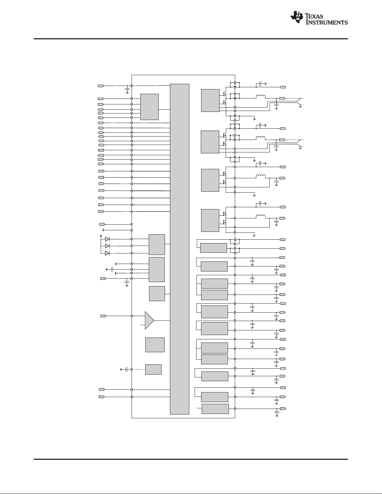
The TPS659122 device provides four configurable step-down converters with up to 2.5A output current for
memory, processor core, I/O, or pre-regulation of LDOs. It also contains 10 LDO regulators for external
usage which can be supplied from either a battery or a pre-regulated supply. Power-up/power-down
controller is configurable and can support any power-up/power-down sequences (OTP based).
TPS659122 integrate a 32 kHz RC Oscillator to sequence all resources during Power up / down. All LDOs
and DCDC converters can be controlled by I2C/SPI interface or Basic ENABLE Balls. In addition, an
Independent automatic Voltage Scaling interface allows transitioning DCDC to different voltage by I2C or
basic Roof/Floor Control. 3 RGB LED with advanced dimming feature are integrated inside the device.
GPIO functionality is multiplexed with LED/ENBLE/SPI when not used. Each GPIO can be configured as
part of the Power up sequence to control external resources. One Sleep pin enables power mode control
between ACTIVE and pre-programmed SLEEP mode for power optimization. For system control the
TPS659122 has 1 comparator for system state management. The TPS659122 comes in a 9 ball x 9 ball
WCSP package (3.6mm x 3.6mm) with a 0.4mm pitch. To request a full data sheet, please send an email
to: pmu_contact@list.ti.com.
Please be aware that an important notice concerning availability, standard warranty, and use in critical applications of
Texas Instruments semiconductor products and disclaimers thereto appears at the end of this data sheet.
Copyright © 2012, Texas Instruments Incorporated
PRODUCTPREVIEW
VBat
VBat
Vbat
SDA_MOSI
SCL_CLK
VINLDO3
LDO3
VDDIO
SW4
DCDC4
2.5A
VDCDC4
1uH
VINDCDC4
10uF
AGND
VREF1V25
100nF
PGND4
SW3
DCDC3
1.6A
VDCDC3
1uH
10uF
PGND3
SW2
DCDC2
0.75A
1uH
VINDCDC2
10uF
PGND2
GPIO2_CE
GPIO1_MISO
I2C/SPI
nPWRON (nRESIN)
nRESPWRON
INT1
SLEEP (PWR_REQ)
PWRHOLD
DGND
VINLDO1210
LDO1
LDO1
(0.8-3.3V, 50mV step
@100mA)
LDO2
LDO2
(0.8-3.3V, 50mV step
@100mA)
VINLDO4
LDO4
LDO4
(1.6-3.3V, 50mV step
@200mA)
Low noise
LDO5
LDO6
VINLDO5
LDO7
LDO7
(0.8-3.3V, 50mV step
@200mA)
LDO8
LDO9
LDO9
(0.8-3.3V, 50mV step
@300mA)
RGB
LED
BIAS
POWER
CONTROL
TPS65912x
32kHz
RC
OSC
ON/OFF
Vth
+
-
SDA_AVS (CLK_REQ2)
SCL_AVS (CLK_REQ1)
EN1 (DCDC1_SEL)
EN2 (DCDC2_SEL)
VINLDO67
LDO5
(1.6-3.3V, 50mV step
@250mA)
Low noise
LDO6
(0.8-3.3V, 50mV step
@100mA)
LDO3
(0.8-3.3V, 50mV step
@100mA)
LDO8
(0.8-3.3V, 50mV step
@100mA)
EN3 (DCDC3_SEL)
EN4 (DCDC4_SEL)
Thermal
warning &
shutdown
LDOAO
Internal
LDO
LEDA/GPIO3
LEDB/GPIO4
LEDC/GPIO5
LDO10
LDO10
(0.8-3.3V, 50mV step
@300mA)
VINLDO
1210
load switch
LSI
LSO
L4
L3
L2
CoutDCDC4
CoutDCDC3
CoutDCDC3
CIN4
CIN3
CIN2
VDCDC4_GND
Vbat
SW1
DCDC1
2.5A
VDCDC1
1uH
VINDCDC1
10uF
PGND1
L1
CoutDCDC1
CIN1
VDCDC1_GND
VINDCDC3
VDCDC2
CoutLDO3
CoutLDO2
CoutLDO1
CoutLDO4
CoutLDO5
CoutLDO6
CoutLDO7
CoutLDO8
CoutLDO9
CoutLDO10
CinLDO67
CinLDO5
CinLDO4
CinLDO1210
CinLDO3
VINLDO8
CinLDO8
VINLDO9
CinLDO9
VCON_PWM
VCON_CLK
OMAP_WDI (32k_OUT)
CONFIG1
CONFIG2
VIN_DCDC_ANA
DEF_SPI_I2C-GPIO
VCC
CPCAP_WDI
AGND
EN_LS0
EN_LS1
CVIN_DCDC_ANA
CVCC
VCCS_VIN_MON
tie to GND
or LDOAO
TPS659122
SWCS079 –JUNE 2012
1.4 Block Diagram & Pin Functions
1.4.1 Functional Block Diagram
2 INTRODUCTION Copyright © 2012, Texas Instruments Incorporated
Figure 1-1. TPS65912x Block Diagram
Submit Documentation Feedback
Product Folder Link(s): TPS659122
www.ti.com
PRODUCTPREVIEW
VLDO7
A1
A2 A3 A4
TPS65912 (bottom view)
B1
C1
D1
VINLDO67 VLDO6 VDCDC4
VDCDC4_
GND
LEDC_
GPIO5
VINDCDC3 EN_LS1 EN_LS0 GPIO2_CE
SW3
CONFIG2 PWRON
GPIO1
_MISO
PGND4
A5
A6
A7
SW4
VINDCDC4 LSO
LSI
VINDCDC4
SW4PGND4
EN4/
DCDC4
_SEL
AGND
VINDCDC
_ANA
SCL_CLK
PWRHOLD
_ON
VDCDC2
EN2 /
DCDC2
_SEL
VINDCDC2
SW2
LSI
PGND3
E1 E2 E3 E4
F1
G1
H1
CONFIG1
DGND
SDA_MOSI
VCON
_PWM
AGNDVDCDC3VINLDO4
VLDO4
VCCS /
VIN_MON
LDOAO
SLEEP /
PWR_REQ
VLDO2 VCC VREF1V25
VDCDC1
_GND
SCL_AVS
CLKREQ1
E5
E7 E8
SDA_AVS
CLKREQ2
DEF_SPI
_I2C
EN1 /
DCDC1
_SEL
VINLDO3VDDIO
OMAP
_WDI
/32kCLK
VCON
_CLK
INT1
nRES
PWRON/
VSUPOUT
CPCAP
_WDI
VINLDO5
PGND1 SW1 VINDCDC1 VINLDO8
PGND2
VLDO5
VLDO8
VLDO3
J1
VLDO10
VINLDO
1210
VLDO1 VDCDC1
PGND1 SW1 VINDCDC1 VINLDO9 VLDO9
A8 A9
LSO
B2 B3
B4
B5
B6 B7 B8 B9
LEDB_
GPIO4
LEDA_
GPIO3
C2 C3
C4 C5 C6
EN3/
DCDC3
_SEL
C7
C8
C9
D2 D3
D4 D5
D6 D7
D8 D9
E6
E9
F2
F3
F4
F5 F6 F7
F8
F9
G2
G3
G4 G5
G6
G7
G8
G9
H2 H3 H4 H5 H6 H7 H8 H9
J9J8J7
J6J5
J4J3
J2
TPS659122
www.ti.com
1.4.2 Pinout
SWCS079 –JUNE 2012
YFF PACKAGE
(BOTTOM VIEW)
Copyright © 2012, Texas Instruments Incorporated INTRODUCTION 3
Product Folder Link(s): TPS659122
Submit Documentation Feedback

PRODUCTPREVIEW
TPS659122
SWCS079 –JUNE 2012
TERMINAL
NAME NO.
TPS659121
REFERENCE
VREF1V25 H3 O
AGND F3, C7 - analog ground connection; connect to PGND on the PCB
DRIVERS / LIGHTING
LEDA/GPIO3 B3 I/O general purpose I/O or LED driver output
LEDB/GPIO4 B2 I/O general purpose I/O or LED driver output
LEDC/GPIO5 B1 I/O general purpose I/O or LED driver output
STEP_DOWN CONVERTERS
VINDCDC_ANA C8 I
VINDCDC1 H7, J7 I
VDCDC1 J4 I voltage sense (feedback) input "+" for DCDC1
VDCDC1_GND H4 I voltage sense (feedback) input "GND" for DCDC1
SW1 H6, J6 O switch node of DCDC1; connect output inductor
PGND1 H5, J5 - power GND connection for DCDC1 converter
VCON_PWM F4 I PWM period signal for dynamic voltage scaling on DCDC1
VCON_CLK F5 I clock signal for dynamic voltage scaling on DCDC1
VINDCDC2 C9 I
VDCDC2 D7 I voltage sense (feedback) input for DCDC2
SW2 D9 O switch node of DCDC2; connect output inductor
PGND2 E9 - power GND connection for DCDC2 converter
VINDCDC3 C1 I
VDCDC3 F2 I voltage sense (feedback) input for DCDC3
SW3 D1 O switch node of DCDC3; connect output inductor
PGND3 E1 - power GND connection for DCDC3 converter
VINDCDC4 A7, B7 I
VDCDC4 A4 I voltage sense (feedback) input "+" for DCDC4
VDCDC4_GND B4 I voltage sense (feedback) input "GND" for DCDC4
SW4 A6, B6 O switch node of DCDC4; connect output inductor
PGND4 A5, B5 - power GND connection for DCDC4 converter
LOAD SWITCH
LSI B8, B9 I input of the load switch
LSO A8, A9 O output of the load switch
EN_LS0 C3 I load switch enable pin; the status is copied to Bit [LOADSWITCH:ENABLE0] in state CONFIG
EN_LS1 C2 I load switch enable pin; the status is copied to Bit [LOADSWITCH:ENABLE1] in state CONFIG
LOW DROPOUT REGULATORS
VINLDO1210 J2 I power input for LDO1, LDO2 and LDO10
VINLDO3 F8 I power input for LDO3
VINLDO4 F1 I power input for LDO4
VINLDO5 G8 I power input for LDO5
VINLDO67 A2 I power input for LDO6 and LDO7
VINLDO8 H8 I power input for LDO8
VINLDO9 J8 I power input for LDO9
www.ti.com
Table 1-1. TERMINAL FUNCTIONS
I/O DESCRIPTION
analog supply input for DCDC converters; needs to be connected to VINDCDC1, VINDCDC2,
VINDCDC3 and VINDCDC4
power input to DCDC1 converter; connect to VINDCDC2, VINDCDC3, VINDCDC4 and
VINDCDC_ANA
power input to DCDC2 converter; connect to VINDCDC1, VINDCDC3, VINDCDC4 and
VINDCDC_ANA
power input to DCDC3 converter; connect to VINDCDC1, VINDCDC2, VINDCDC4 and
VINDCDC_ANA
power input to DCDC4 converter; connect to VINDCDC1, VINDCDC2, VINDCDC3 and
VINDCDC_ANA
4 INTRODUCTION Copyright © 2012, Texas Instruments Incorporated
Submit Documentation Feedback
Product Folder Link(s): TPS659122

PRODUCTPREVIEW
TPS659122
www.ti.com
TERMINAL
NAME NO.
TPS659121
LDOAO G3 O "LDO always on" internal supply; connect buffer capacitor
VLDO1 J3 O LDO1 output
VLDO2 H1 O LDO2 output
VLDO3 F9 O LDO3 output
VLDO4 G1 O LDO4 output
VLDO5 G9 O LDO5 output
VLDO6 A3 O LDO6 output
VLDO7 A1 O LDO7 output
VLDO8 H9 O LDO8 output
VLDO9 J9 O LDO9 output
VLDO10 J1 O LDO10 output
STANDARD INTERFACE
DEF_SPI_I2C-GPIO E7 I
SCK D5 I I2C SCL for DEF_SPI_I2C=1 or SPI SCK for DEF_SPI_I2C=0
MOSI E4 I/O I2C SDA for DEF_SPI_I2C=1 or SPI MASTER OUT SLAVE IN (MOSI) for DEF_SPI_I2C=0
MISO D4 I/O GPIO1 for DEF_SPI_I2C=1 or SPI MASTER IN SLAVE OUT (MISO) for DEF_SPI_I2C=0
CE C4 I/O GPIO2 for DEF_SPI_I2C=1 or SPI CHIP ENABLE (CE) active HIGH for DEF_SPI_I2C=0
ENABLE / VOLTAGE SCALING
DCDC1_SEL E8 I
DCDC2_SEL D8 I
DCDC3_SEL C6 I
DCDC4_SEL C5 I
CLK_REQ1 E5 I
CLK_REQ2 E6 I/O
PWR_REQ G4 I SLEEP mode input or CLK request input
VSUP_OUT G6 O Reset output or output of voltage monitor
VIN_MON G2 I voltage sense for input voltage monitor; output on pin VSUP_OUT
ON D6 I POWERHOLD or ON; enable input
INT1 G5 O interrupt output
RESIN (optional) D3 I alternatively active low reset input to TPS65912x; debounced by 10ms(OTP option); tie to
OMAP_WDI_32k_OU
T
CPCAP_WDI G7 O push-pull output at VDDIO level of AND gate; connect to CPCAP WDI input
CONFIG1 E2 I
CONFIG2 D2 I and DCDC4_SEL as well as CLK_REQ and PWR_REQ signals with CONFIG2 tied to GND. Tie
F6 I input from OMAP WDI pin to AND gate; alternatively 32kHz RC oscillator output. The option is
SWCS079 –JUNE 2012
Table 1-1. TERMINAL FUNCTIONS (continued)
I/O DESCRIPTION
digital input that defines whether SPI or I2C and GPIOs is available on pins C4, D4, E4, D5:
0=SPI; 1=I2C and GPIO1 and GPIO2
DCDCx_SEL is selected by pulling pin CONFIG2 to GND; this also selects CLK_REQx and
PWR_REQ as enable resources
enable pin or voltage scaling pin changing the output of a converter or a group of converters
between 2 pre-defined values
enable pin or voltage scaling pin changing the output of a converter or a group of converters
between 2 pre-defined values
enable pin or voltage scaling pin changing the output of a converter or a group of converters
between 2 pre-defined values
enable pin or voltage scaling pin changing the output of a converter or a group of converters
between 2 pre-defined values
CLK-REQ1, CLK_REQ2 and PWR_REQ is selected by puling pin CONFIG2 to GND
power I2C for dynamic voltage scaling: clock pin or clock request signal1 used to enable and
disable power resources
power I2C for dynamic voltage scaling; data pin or clock request signal2 used to enable and
disable power resources
active low, debounced power-on input or power request input to start power-up sequencing;
LDOAO for a logic high if not used.
selects pre-defined startup options and default voltages; chooses from two internal OTP settings;
tie to GND or LDOAO
selects pre-defined startup options; configures pins as DCDC1_SEL, DCDC2_SEL, DCDC3_SEL
to LDOAO for a logic high level.
Copyright © 2012, Texas Instruments Incorporated INTRODUCTION 5
Submit Documentation Feedback
Product Folder Link(s): TPS659122

PRODUCTPREVIEW
TPS659122
SWCS079 –JUNE 2012
www.ti.com
Table 1-1. TERMINAL FUNCTIONS (continued)
TERMINAL
NAME NO.
TPS659121
VCC H2 I digital supply input
VDDIO F7 I supply voltage input for GPIOs and output stages that sets the HIGH level voltage (I/O voltage)
DGND E3 - digital GND connection, tie to AGND and PGNDx on the pcb
I/O DESCRIPTION
6 INTRODUCTION Copyright © 2012, Texas Instruments Incorporated
Submit Documentation Feedback
Product Folder Link(s): TPS659122

PACKAGE OPTION ADDENDUM
www.ti.com
19-Dec-2012
PACKAGING INFORMATION
Orderable Device Status
TPS659122YFFR ACTIVE DSBGA YFF 81 1500 Green (RoHS
TPS659122YFFT ACTIVE DSBGA YFF 81 250 Green (RoHS
(1)
The marketing status values are defined as follows:
ACTIVE: Product device recommended for new designs.
LIFEBUY: TI has announced that the device will be discontinued, and a lifetime-buy period is in effect.
NRND: Not recommended for new designs. Device is in production to support existing customers, but TI does not recommend using this part in a new design.
PREVIEW: Device has been announced but is not in production. Samples may or may not be available.
OBSOLETE: TI has discontinued the production of the device.
Package Type Package
(1)
Drawing
Pins Package Qty Eco Plan
(2)
& no Sb/Br)
& no Sb/Br)
Lead/Ball Finish MSL Peak Temp
(3)
SNAGCU Level-1-260C-UNLIM
SNAGCU Level-1-260C-UNLIM
Samples
(Requires Login)
(2)
Eco Plan - The planned eco-friendly classification: Pb-Free (RoHS), Pb-Free (RoHS Exempt), or Green (RoHS & no Sb/Br) - please check http://www.ti.com/productcontent for the latest availability
information and additional product content details.
TBD: The Pb-Free/Green conversion plan has not been defined.
Pb-Free (RoHS): TI's terms "Lead-Free" or "Pb-Free" mean semiconductor products that are compatible with the current RoHS requirements for all 6 substances, including the requirement that
lead not exceed 0.1% by weight in homogeneous materials. Where designed to be soldered at high temperatures, TI Pb-Free products are suitable for use in specified lead-free processes.
Pb-Free (RoHS Exempt): This component has a RoHS exemption for either 1) lead-based flip-chip solder bumps used between the die and package, or 2) lead-based die adhesive used between
the die and leadframe. The component is otherwise considered Pb-Free (RoHS compatible) as defined above.
Green (RoHS & no Sb/Br): TI defines "Green" to mean Pb-Free (RoHS compatible), and free of Bromine (Br) and Antimony (Sb) based flame retardants (Br or Sb do not exceed 0.1% by weight
in homogeneous material)
(3)
MSL, Peak Temp. -- The Moisture Sensitivity Level rating according to the JEDEC industry standard classifications, and peak solder temperature.
Important Information and Disclaimer:The information provided on this page represents TI's knowledge and belief as of the date that it is provided. TI bases its knowledge and belief on information
provided by third parties, and makes no representation or warranty as to the accuracy of such information. Efforts are underway to better integrate information from third parties. TI has taken and
continues to take reasonable steps to provide representative and accurate information but may not have conducted destructive testing or chemical analysis on incoming materials and chemicals.
TI and TI suppliers consider certain information to be proprietary, and thus CAS numbers and other limited information may not be available for release.
In no event shall TI's liability arising out of such information exceed the total purchase price of the TI part(s) at issue in this document sold by TI to Customer on an annual basis.
Addendum-Page 1

PACKAGE MATERIALS INFORMATION
www.ti.com 19-Dec-2012
TAPE AND REEL INFORMATION
*All dimensions are nominal
Device Package
TPS659122YFFR DSBGA YFF 81 1500 180.0 12.4 3.79 3.79 0.71 8.0 12.0 Q1
TPS659122YFFT DSBGA YFF 81 250 180.0 12.4 3.79 3.79 0.71 8.0 12.0 Q1
Type
Package
Drawing
Pins SPQ Reel
Diameter
(mm)
Reel
Width
W1 (mm)
A0
(mm)B0(mm)K0(mm)P1(mm)W(mm)
Pin1
Quadrant
Pack Materials-Page 1

PACKAGE MATERIALS INFORMATION
www.ti.com 19-Dec-2012
*All dimensions are nominal
Device Package Type Package Drawing Pins SPQ Length (mm) Width (mm) Height (mm)
TPS659122YFFR DSBGA YFF 81 1500 210.0 185.0 35.0
TPS659122YFFT DSBGA YFF 81 250 210.0 185.0 35.0
Pack Materials-Page 2

IMPORTANT NOTICE
Texas Instruments Incorporated and its subsidiaries (TI) reserve the right to make corrections, enhancements, improvements and other
changes to its semiconductor products and services per JESD46, latest issue, and to discontinue any product or service per JESD48, latest
issue. Buyers should obtain the latest relevant information before placing orders and should verify that such information is current and
complete. All semiconductor products (also referred to herein as “components”) are sold subject to TI’s terms and conditions of sale
supplied at the time of order acknowledgment.
TI warrants performance of its components to the specifications applicable at the time of sale, in accordance with the warranty in TI’s terms
and conditions of sale of semiconductor products. Testing and other quality control techniques are used to the extent TI deems necessary
to support this warranty. Except where mandated by applicable law, testing of all parameters of each component is not necessarily
performed.
TI assumes no liability for applications assistance or the design of Buyers’ products. Buyers are responsible for their products and
applications using TI components. To minimize the risks associated with Buyers’ products and applications, Buyers should provide
adequate design and operating safeguards.
TI does not warrant or represent that any license, either express or implied, is granted under any patent right, copyright, mask work right, or
other intellectual property right relating to any combination, machine, or process in which TI components or services are used. Information
published by TI regarding third-party products or services does not constitute a license to use such products or services or a warranty or
endorsement thereof. Use of such information may require a license from a third party under the patents or other intellectual property of the
third party, or a license from TI under the patents or other intellectual property of TI.
Reproduction of significant portions of TI information in TI data books or data sheets is permissible only if reproduction is without alteration
and is accompanied by all associated warranties, conditions, limitations, and notices. TI is not responsible or liable for such altered
documentation. Information of third parties may be subject to additional restrictions.
Resale of TI components or services with statements different from or beyond the parameters stated by TI for that component or service
voids all express and any implied warranties for the associated TI component or service and is an unfair and deceptive business practice.
TI is not responsible or liable for any such statements.
Buyer acknowledges and agrees that it is solely responsible for compliance with all legal, regulatory and safety-related requirements
concerning its products, and any use of TI components in its applications, notwithstanding any applications-related information or support
that may be provided by TI. Buyer represents and agrees that it has all the necessary expertise to create and implement safeguards which
anticipate dangerous consequences of failures, monitor failures and their consequences, lessen the likelihood of failures that might cause
harm and take appropriate remedial actions. Buyer will fully indemnify TI and its representatives against any damages arising out of the use
of any TI components in safety-critical applications.
In some cases, TI components may be promoted specifically to facilitate safety-related applications. With such components, TI’s goal is to
help enable customers to design and create their own end-product solutions that meet applicable functional safety standards and
requirements. Nonetheless, such components are subject to these terms.
No TI components are authorized for use in FDA Class III (or similar life-critical medical equipment) unless authorized officers of the parties
have executed a special agreement specifically governing such use.
Only those TI components which TI has specifically designated as military grade or “enhanced plastic” are designed and intended for use in
military/aerospace applications or environments. Buyer acknowledges and agrees that any military or aerospace use of TI components
which have not been so designated is solely at the Buyer's risk, and that Buyer is solely responsible for compliance with all legal and
regulatory requirements in connection with such use.
TI has specifically designated certain components as meeting ISO/TS16949 requirements, mainly for automotive use. In any case of use of
non-designated products, TI will not be responsible for any failure to meet ISO/TS16949.
Products Applications
Audio www.ti.com/audio Automotive and Transportation www.ti.com/automotive
Amplifiers amplifier.ti.com Communications and Telecom www.ti.com/communications
Data Converters dataconverter.ti.com Computers and Peripherals www.ti.com/computers
DLP® Products www.dlp.com Consumer Electronics www.ti.com/consumer-apps
DSP dsp.ti.com Energy and Lighting www.ti.com/energy
Clocks and Timers www.ti.com/clocks Industrial www.ti.com/industrial
Interface interface.ti.com Medical www.ti.com/medical
Logic logic.ti.com Security www.ti.com/security
Power Mgmt power.ti.com Space, Avionics and Defense www.ti.com/space-avionics-defense
Microcontrollers microcontroller.ti.com Video and Imaging www.ti.com/video
RFID www.ti-rfid.com
OMAP Applications Processors www.ti.com/omap TI E2E Community e2e.ti.com
Wireless Connectivity www.ti.com/wirelessconnectivity
Mailing Address: Texas Instruments, Post Office Box 655303, Dallas, Texas 75265
Copyright © 2012, Texas Instruments Incorporated
 Loading...