

Datasheet TPS659101A1RSL, TPS659102A1RSL, TPS659103A1RSL, TPS659104A1RSL, TPS659105A1RSL Datasheet (Texas Instruments) [ru]
...
TPS65910, TPS65910A, TPS65910A3, TPS659101, TPS659102, TPS659103
TPS659104, TPS659105, TPS659106, TPS659107, TPS659108, TPS659109
www.ti.com
SWCS046T –MARCH 2010–REVISED SEPTEMBER 2013
Integrated Power Management Unit Top Specification
Check for
Samples: TPS65910, TPS65910A, TPS65910A3, TPS659101, TPS659102, TPS659103, TPS659104, TPS659105, TPS659106,
1
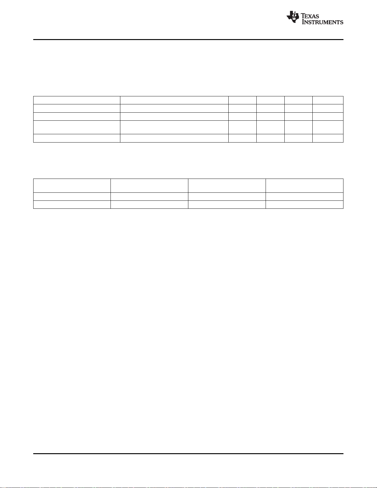
FEATURES
The purpose of the TPS65910 device is to
provide the following resources:
• Embedded power controller
• Two efficient step-down dc-dc converters for
processor cores
• One efficient step-down dc-dc converter for I/O
power
• One efficient step-up 5-V dc-dc converter
• SmartReflex™ compliant dynamic voltage
management for processor cores
• 8 LDO voltage regulators and one RTC LDO
(internal purpose)
• One high-speed I2C interface for generalpurpose control commands (CTL-I2C)
• One high-speed I2C interface for SmartReflex
Class 3 control and command (SR-I2C)
• Two enable signals multiplexed with SR-I2C,
configurable to control any supply state and
processor cores supply voltage
• Thermal shutdown protection and hot-die
detection
• A real-time clock (RTC) resource with:
– Oscillator for 32.768-kHz crystal or 32-kHz
built-in RC oscillator
– Date, time and calendar
– Alarm capability
• One configurable GPIO
• DC-DC switching synchronization through
internal or external 3-MHz clock
TPS659107, TPS659108, TPS659109
APPLICATIONS
• Portable and handheld systems
• OMAP3 power management
DESCRIPTION
The TPS65910 is an integrated power-management
IC available in 48-QFN package and dedicated to
applications powered by one Li-Ion or Li-Ion polymer
battery cell or 3-series Ni-MH cells, or by a 5-V input;
it requires multiple power rails. The device provides
three step-down converters, one step-up converter,
and eight LDOs and is designed to support the
specific power requirements of OMAP-based
applications.
Two of the step-down converters provide power for
dual processor cores and are controllable by a
dedicated class-3 SmartReflex interface for optimum
power savings. The third converter provides power for
the I/Os and memory in the system.
The device includes eight general-purpose LDOs
providing a wide range of voltage and current
capabilities; they are fully controllable by the I2C
interface. The use of the LDOs is flexible; they are
intended to be used as follows: Two LDOs are
designated to power the PLL and video DAC supply
rails on the OMAP based processors, four generalpurpose auxiliary LDOs are available to provide
power to other devices in the system, and two LDOs
are provided to power DDR memory supplies in
applications requiring these memories.
In addition to the power resources, the device
contains an embedded power controller (EPC) to
manage the power sequencing requirements of the
OMAP systems and an (RTC).
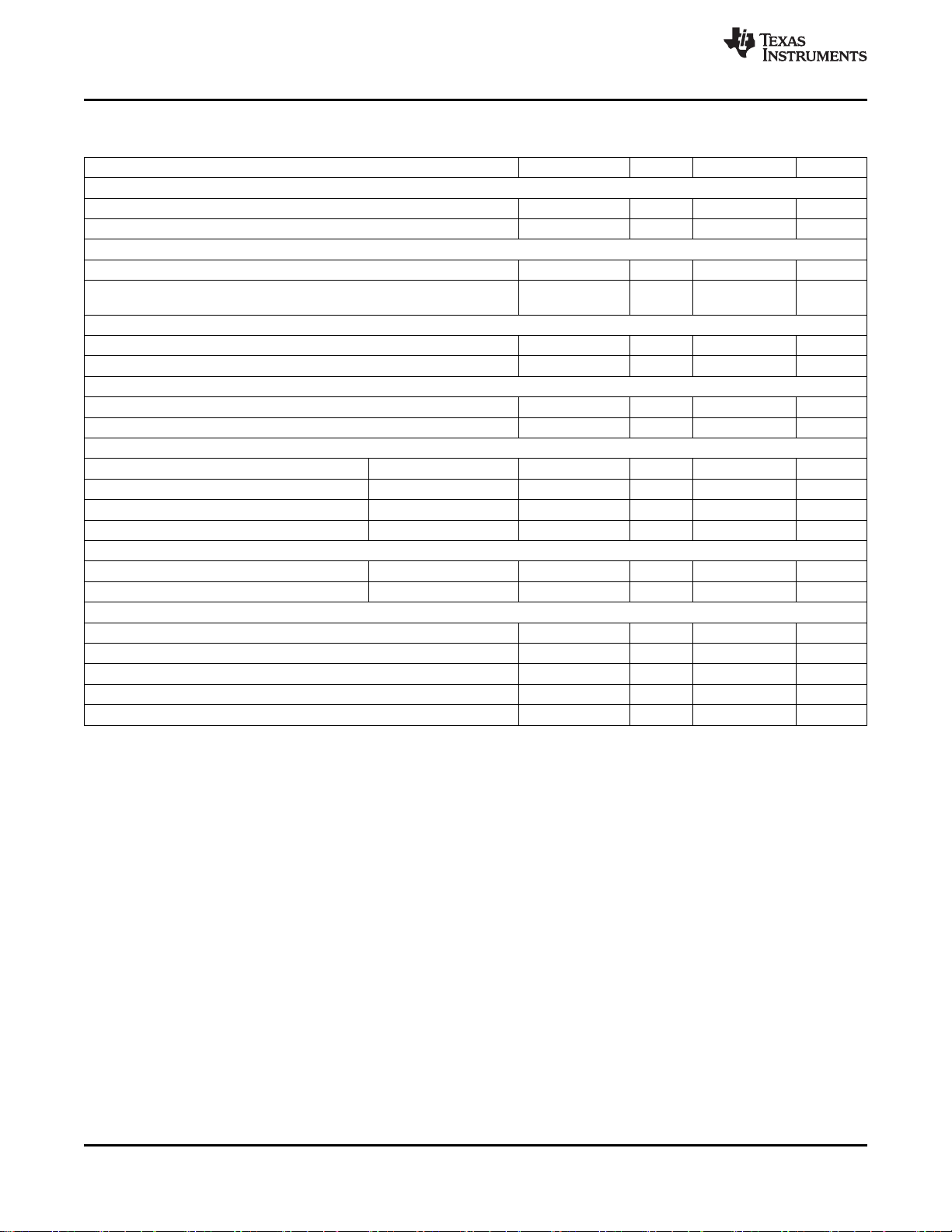
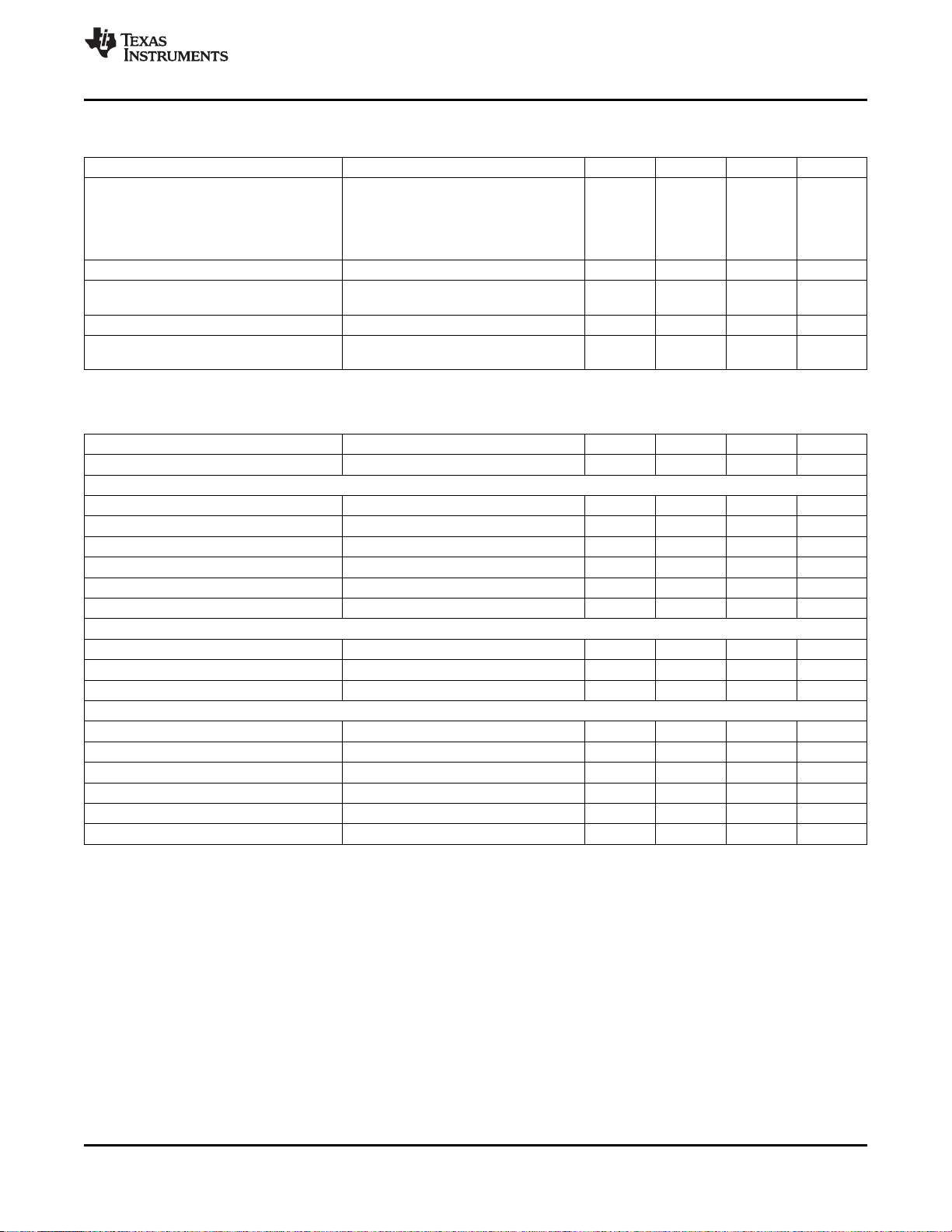
Figure 1 shows the top-level diagram of the device.
1
Please be aware that an important notice concerning availability, standard warranty, and use in critical applications of
Texas Instruments semiconductor products and disclaimers thereto appears at the end of this data sheet.
PRODUCTION DATA information is current as of publication date.
Products conform to specifications per the terms of the Texas
Instruments standard warranty. Production processing does not
necessarily include testing of all parameters.
Copyright © 2010–2013, Texas Instruments Incorporated
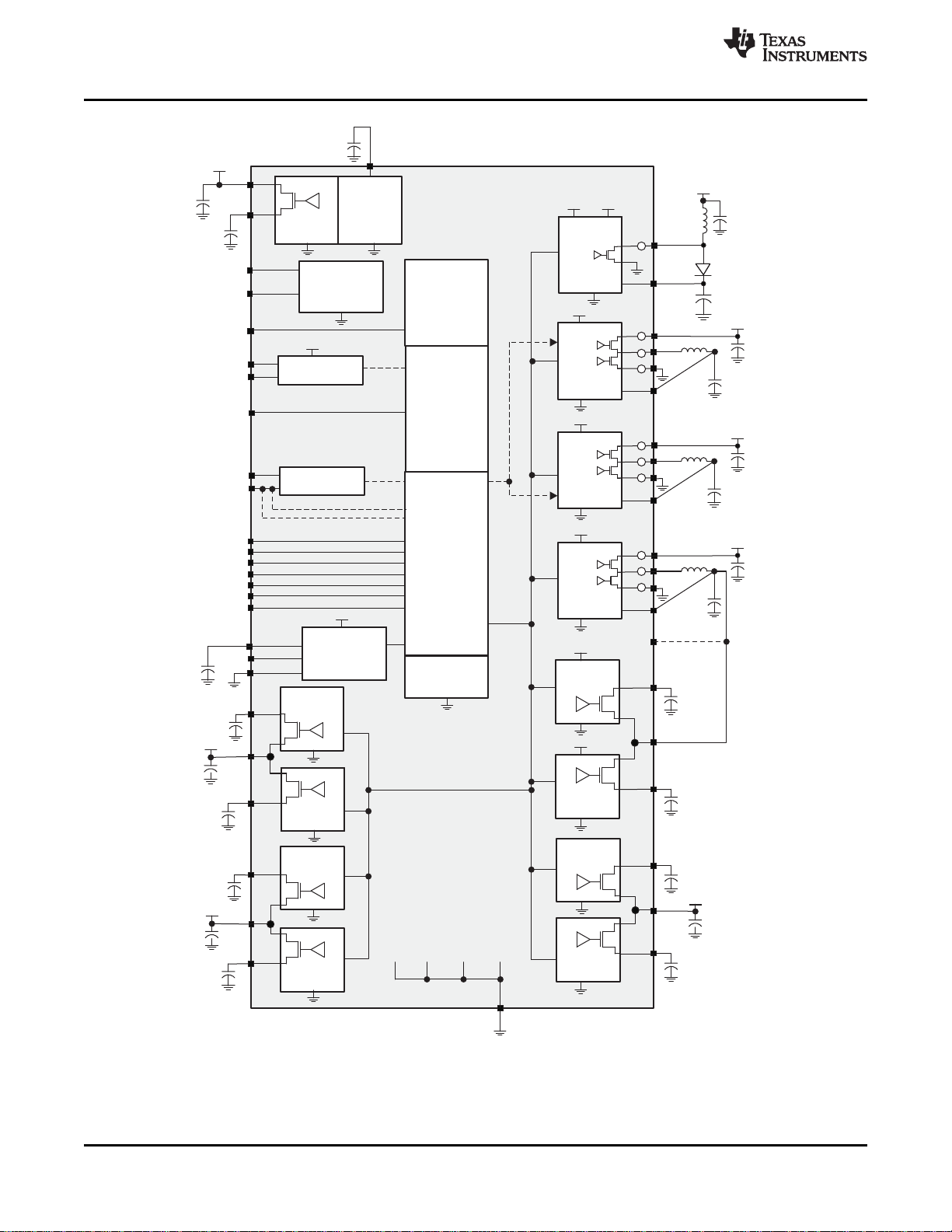
VFB1
INT1
PWRON
VREF
REFGND
Test interface
CLK32KOUT
VAUX33
VMMC
OSC32KIN
OSC32KOUT
TESTV
SLEEP
NRESPWRON
PWRHOLD
BOOT1
BOOT0
SDASR_EN2
SCLSR_EN1
SDA_SDI
VDAC
VPLL
VAUX1
VRTC
Real-time
clock
VFB3
SW3
VDIG2
VAUX2
VDIG1
VDD1
(SMPS)
VCC1
GND1
SW1
VFBIO
VBAT
VCC7
VCC7
VCC7
VBAT
VBAT
VBAT
VCC6
VCC3
VCC4
VCC5
VCC 7
VBAT
VCC7
VDDIO
VDDIO
AGND2
AGND
AGND
GNDA
GNDA
DGND
VAUX33
REFGND
GND3
OSC
32-kHz
SCL_SCK
Bus
control
GPIO_CKSYNC
Power
control
state-
machine
Analog
references
and comparators
VBACKUP
Backup
management
VRTC (LDO)
and POR
VFB2
VCC2
GND2
SW2
VCCIO
GNDIO
SWIO
GNDP
AGND
AGND2
AGND2
VDAC
(LDO)
VPLL
(LDO)
VAUX1
(LDO)
VAUX2
(LDO)
VDIG1
(LDO)
AGND2
AGND2
AGND2
VDIG2
(LDO)
VAUX33
(LDO)
VMMC
(LDO)
I C
2
I C
2
AGND2
AGND
AGND
VCC7
VCC7
VCC4
VDD2
(SMPS)
VIO
(SMPS)
VDD3
(SMPS)
SWCS046-001
GNDP: Power pad ground
Ci
(VCC7)
Co
(VRTC)
Co
(VREF)
Co
(VDAC)
Ci
(VCC5)
C
BB
Co
(VPLL)
Co
(VAUX1)
Ci
(VCC4)
Co
(VAUX2)
DGND AGND AGND2
GND3
Co
(VMMC)
VBAT
Ci
(VCC4)
Co
(VAUX33)
Co
(VDIG2)
Co
(VDIG1)
Co
(VIO)
Ci
(VCCIO)
VBAT
Ci
(VCC2)
Co
(VDD2)
VBAT
Ci
(VCC1)
Co
(VDD1)
Co
(VDD3)
Ci
(VDD3)
TPS65910, TPS65910A, TPS65910A3, TPS659101, TPS659102, TPS659103
TPS659104, TPS659105, TPS659106, TPS659107, TPS659108, TPS659109
SWCS046T –MARCH 2010–REVISED SEPTEMBER 2013
2 Submit Documentation Feedback Copyright © 2010–2013, Texas Instruments Incorporated
Product Folder Links: TPS65910 TPS65910A TPS65910A3 TPS659101 TPS659102 TPS659103 TPS659104
Figure 1. 48-QFN Top-Level Diagram
TPS659105 TPS659106 TPS659107 TPS659108 TPS659109
www.ti.com
TPS65910, TPS65910A, TPS65910A3, TPS659101, TPS659102, TPS659103
TPS659104, TPS659105, TPS659106, TPS659107, TPS659108, TPS659109
www.ti.com
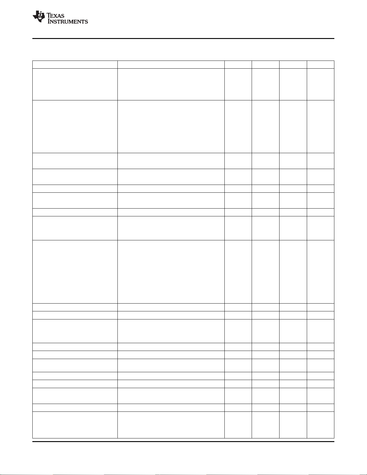
Table 1. SUPPORTED PROCESSORS AND CORRESPONDING PART NUMBERS
Compatible Processor
TI processor - AM335x with DDR2 TPS65910AA1RSL
TI processor - AM335x with DDR3 TPS65910A3A1RSL
TI processor - AM335x with DDR3
TI processors - AM1705/07, AM1806/08, AM3505/17, AM3703/15, DM3730/25, TPS65910A1RSL
OMAP-L137/38, OMAP3503/15/25/30, TMS320C6742/6/8
Samsung - S5PV210, S5PC110 TPS659101A1RSL
Rockchip - RK29xx, RK30xx TPS659102A1RSL
Samsung - S5PC100 TPS659103A1RSL
Samsung - S5P6440 TPS659104A1RSL
TI processors - DM643x, DM644x TPS659105A1RSL
Reserved TPS659106A1RSL
Freescale - i.MX27, Freescale - i.MX35 TPS659107A1RSL
Freescale - i.MX508 TPS659108A1RSL
Freescale - i.MX51 TPS659109A1RSL
(1) The RSL package is available in tape and reel. See for details for corresponding part numbers, quantities and ordering information.
(2) Refer to SWCU093 document.
(1)
(2)
SWCS046T –MARCH 2010–REVISED SEPTEMBER 2013
Part Number
TPS65910A31A1RSL
(1)
ABSOLUTE MAXIMUM RATINGS
over operating free-air temperature range (unless otherwise noted)
Stresses beyond those listed under below may cause permanent damage to the device. These are stress ratings only and
functional operation of the device at these or any other conditions beyond those indicated below are not implied. Exposure to
absolute-maximum-rated conditions for extended periods may affect device reliability.
The absolute maximum ratings for the TPS65910 device are listed below:
PARAMETER MIN MAX UNIT
Voltage range on pins/balls VCC1, VCC2, VCCIO, VCC3, VCC4,
VCC5, VCC6, VCC7
Voltage range on pins/balls VDDIO –0.3 3.6 V
Voltage range on pins/balls OSC32KIN, OSC32KOUT, BOOT1,
BOOT0
Voltage range on pins/balls SDA_SDI, SCL_SCK, SDASR_EN2,
SCLSR_EN1, SLEEP, INT1, CLK32KOUT, NRESPWRON
Voltage range on pins/balls PWRON –0.3 7 V
Voltage range on pins/balls PWRHOLD
Functional junction temperature range –45 150 °C
Peak output current on all other terminals than power resources –5 5 mA
(1) I/O supplied from VDDIO but which can be driven from to a VBAT voltage level
(2) I/O supplied from VRTC but can be driven to a VBAT voltage level
(1)
GPIO_CKSYNC
(2)
–0.3 7 V
–0.3 VRTC
–0.3 VDDIO
–0.3 7 V
+ 0.3 V
MAX
+ 0.3 V
MAX
THERMAL CHARACTERISTICS
over operating free-air temperature range (unless otherwise noted)
Package R
RSL 48-QFN 37 2.6 37 1.48 1
θja
(°C/W)
TA < 25°C Power FACTOR ABOVE TA = 70°C Power TA = 85°C Power
Rating (W) 25 °C (W) Rating (W)
DERATING
(mW/°C)
The thermal resistance R
The value of thermal resistance R
Copyright © 2010–2013, Texas Instruments Incorporated Submit Documentation Feedback 3
Product Folder Links: TPS65910 TPS65910A TPS65910A3 TPS659101 TPS659102 TPS659103 TPS659104
junction-to-power PAD of the RSL package is 1.1°C/W
θJP
junction-to-ambient was measured on a high K.
θJA
TPS659105 TPS659106 TPS659107 TPS659108 TPS659109
TPS65910, TPS65910A, TPS65910A3, TPS659101, TPS659102, TPS659103
TPS659104, TPS659105, TPS659106, TPS659107, TPS659108, TPS659109
SWCS046T –MARCH 2010–REVISED SEPTEMBER 2013
RECOMMENDED OPERATING CONDITIONS
over operating free-air temperature range (unless otherwise noted)
Lists of the recommended operating maximum ratings for the TPS65910 device are given below.
Note1: VCC7 should be connected to the highest supply that is connected to the device VCCx pin. The exception is that
VCC2 and VCC4 can be higher than VCC7.
Note2: VCC2 and VCC4 must be connected together (to the same voltage).
Note3: If VDD3 boost is used, VAUX33 must be set to 2.8 V or higher and enabled before VDD3.
PARAMETER TEST CONDITIONS MIN NOM MAX UNIT
VCC: Input voltage range on pins/balls VCC1, VCC2, VCCIO, VCC3, VCC4, VCC5,
VCC7
V
: Input voltage range on pins/balls VCC6 1.7 3.6 5.5 V
CCP
Input voltage range on pins/balls VDDIO 1.65 1.8/3.3 3.45 V
Input voltage range on pins/balls PWRON 0 3.6 5.5 V
Input voltage range on pins/balls SDA_SDI, SCL_SCK, SDASR_EN2, SCLSR_EN1,
SLEEP
Input voltage range on pins/balls PWRHOLD, GPIO_CKSYNC 1.65 VDDIO 5.5 V
Input voltage range on balls BOOT1, BOOT0, OSC32KIN 1.65 VRTC 1.95 V
Operating free-air temperature, T
Junction temperature T
J
A
Storage temperature range –65 27 150 °C
Lead temperature (soldering, 10 s) 260 °C
Power References
VREF filtering capacitor C
O(VREF)
Connected from VREF to REFGND 100 nF
VDD1 SMPS
Input capacitor C
Filter capacitor C
I(VCC1)
O(VDD1)
X5R or X7R dielectric 10 µF
X5R or X7R dielectric 4 10 12 µF
COfilter capacitor ESR f = 3 MHz 10 300 mΩ
Inductor L
LOinductor dc resistor DCR
O(VDD1)
L
VDD2 SMPS
Input capacitor C
Filter capacitor C
I(VCC2)
O(VDD2)
X5R or X7R dielectric 10 µF
X5R or X7R dielectric 4 10 12 µF
COfilter capacitor ESR f = 3 MHz 10 300 mΩ
Inductor L
LOinductor dc resistor DCR
O(VDD2)
L
VIO SMPS
Input capacitor C
Filter capacitor C
I(VIO)
O(VIO)
X5R or X7R dielectric 10 µF
X5R or X7R dielectric 4 10 12 µF
COfilter capacitor ESR f = 3 MHz 10 300 mΩ
Inductor L
LOinductor dc resistor DCR
O(VIO)
L
VDIG1 LDO
Input capacitor C
I(VCC6)
Filtering capacitor C
O(VDIG1)
X5R or X7R dielectric 4.7 µF
COfiltering capacitor ESR 0 500 mΩ
VDIG2 LDO
Filtering capacitor C
O(VDIG2)
COfiltering capacitor ESR 0 500 mΩ
VPLL LDO
Input capacitor C
I(VCC5)
Filtering capacitor C
O(VPLL)
X5R or X7R dielectric 4.7 µF
2.7 3.6 5.5 V
1.65 VDDIO 3.45 V
–40 27 85 °C
–40 27 125 °C
2.2 µH
125 mΩ
2.2 µH
125 mΩ
2.2 µH
125 mΩ
0.8 2.2 2.64 µF
0.8 2.2 2.64 µF
0.8 2.2 2.64 µF
www.ti.com
4 Submit Documentation Feedback Copyright © 2010–2013, Texas Instruments Incorporated
Product Folder Links: TPS65910 TPS65910A TPS65910A3 TPS659101 TPS659102 TPS659103 TPS659104
TPS659105 TPS659106 TPS659107 TPS659108 TPS659109
TPS65910, TPS65910A, TPS65910A3, TPS659101, TPS659102, TPS659103
TPS659104, TPS659105, TPS659106, TPS659107, TPS659108, TPS659109
www.ti.com
RECOMMENDED OPERATING CONDITIONS (continued)
over operating free-air temperature range (unless otherwise noted)
Lists of the recommended operating maximum ratings for the TPS65910 device are given below.
Note1: VCC7 should be connected to the highest supply that is connected to the device VCCx pin. The exception is that
VCC2 and VCC4 can be higher than VCC7.
Note2: VCC2 and VCC4 must be connected together (to the same voltage).
Note3: If VDD3 boost is used, VAUX33 must be set to 2.8 V or higher and enabled before VDD3.
PARAMETER TEST CONDITIONS MIN NOM MAX UNIT
COfiltering capacitor ESR 0 500 mΩ
VDAC LDO
Filtering capacitor C
COfiltering capacitor ESR 0 500 mΩ
Input capacitor C
Filtering capacitor C
COfiltering capacitor ESR 0 500 mΩ
Filtering capacitor C
COfiltering capacitor ESR 0 500 mΩ
Input capacitor C
Filtering capacitor C
COfiltering capacitor ESR 0 500 mΩ
Filtering capacitor C
COfiltering capacitor ESR 0 500 mΩ
Input capacitor C
Filtering capacitor C
COfiltering capacitor ESR 0 500 mΩ
Input capacitor C
Filter capacitor C
COfilter capacitor ESR f = 1 MHz 10 300 mΩ
Inductor L
O(VDD3)
LOinductor DC resistor DCR
Backup battery capacitor C
Series resistors Ω
SDA_SDI, SCL_SCK, SDASR_EN2,
SCLSR_EN1 external pull-up resistor
Crystal frequency @ specified load cap value 32.768 kHz
Crystal tolerance @ 27°C –20 0 20 ppm
Frequency Temperature coefficient. –0.5 0.5 ppm/°C
Secondary temperature coefficient –0.04 –0.035 –0.03 ppm/°C
Voltage coefficient –2 2 ppm/V
O(VDAC)
I(VCC4)
O(VMMC)
O(VAUX33)
I(VCC3)
O(VAUX1)
O(VAUX2)
I(VCC7)
O(VRTC)
I(VDD3)
O(VDD3)
VMMC LDO
X5R or X7R dielectric 4.7 µF
VAUX33 LDO
VAUX1 LDO
X5R or X7R dielectric 4.7 µF
VAUX2 LDO
VRTC LDO
X5R or X7R dielectric 4.7 µF
VDD3 SMPS
X5R or X7R dielectric 4.7 µF
X5R or X7R dielectric 4 10 12 µF
L
Backup Battery
Battery or superCap supplying VBACKUP 5 10 2000 mF
BB
Capacitor supplying VBACKUP 1 40 µF
5 to 15 mF 10 1500
100 to 2000 mF 5 15
I2C Interfaces
Connected to VDDIO 1.2 kΩ
Crystal Oscillator (connected from OSC32KIN to OSC32KOUT)
Oscillator contribution (not including crystal
variation)
SWCS046T –MARCH 2010–REVISED SEPTEMBER 2013
0.8 2.2 2.64 µF
0.8 2.2 2.64 µF
0.8 2.2 2.64 µF
0.8 2.2 2.64 µF
0.8 2.2 2.64 µF
0.8 2.2 2.64 µF
2.8 4.7 6.6 µH
50 500 mΩ
2
Copyright © 2010–2013, Texas Instruments Incorporated Submit Documentation Feedback 5
Product Folder Links: TPS65910 TPS65910A TPS65910A3 TPS659101 TPS659102 TPS659103 TPS659104
TPS659105 TPS659106 TPS659107 TPS659108 TPS659109
TPS65910, TPS65910A, TPS65910A3, TPS659101, TPS659102, TPS659103
TPS659104, TPS659105, TPS659106, TPS659107, TPS659108, TPS659109
SWCS046T –MARCH 2010–REVISED SEPTEMBER 2013
RECOMMENDED OPERATING CONDITIONS (continued)
over operating free-air temperature range (unless otherwise noted)
Lists of the recommended operating maximum ratings for the TPS65910 device are given below.
Note1: VCC7 should be connected to the highest supply that is connected to the device VCCx pin. The exception is that
VCC2 and VCC4 can be higher than VCC7.
Note2: VCC2 and VCC4 must be connected together (to the same voltage).
Note3: If VDD3 boost is used, VAUX33 must be set to 2.8 V or higher and enabled before VDD3.
PARAMETER TEST CONDITIONS MIN NOM MAX UNIT
Max crystal series resistor @ Fundamental frequency 90 kΩ
Crystal load capacitor According to crystal data sheet 6 12.5 pF
Load crystal oscillator Coscin
,Coscout
Quality factor 8000 80000
parallel mode Including parasitic PCB capacitor 12 25 pF
ESD SPECIFICATIONS
over operating free-air temperature range (unless otherwise noted)
ESD METHOD STANDARD REFERENCE PERFORMANCE
Human body model (HBM) EIA/JESD22-A114D 2000 V 2000 V
Charge device model (CDM) EIA/JESD22-C101C 500 V 500 V
TI STANDARD
REQUIREMENTS
www.ti.com
6 Submit Documentation Feedback Copyright © 2010–2013, Texas Instruments Incorporated
Product Folder Links: TPS65910 TPS65910A TPS65910A3 TPS659101 TPS659102 TPS659103 TPS659104
TPS659105 TPS659106 TPS659107 TPS659108 TPS659109
TPS65910, TPS65910A, TPS65910A3, TPS659101, TPS659102, TPS659103
TPS659104, TPS659105, TPS659106, TPS659107, TPS659108, TPS659109
www.ti.com
I/O PULLUP AND PULLDOWN CHARACTERISTICS
over operating free-air temperature range (unless otherwise noted)
PARAMETER TEST CONDITIONS MIN TYP MAX UNIT
SDA_SDI, SCL_SCK, SDASR_EN2,
SCLSR_EN1 Programmable pullup (DFT, default Grounded, VDDIO = 1.8 V –45% 8 +45% kΩ
inactive)
SLEEP programmable pulldown (default active) @ 1.8 V, VRTC = 1.8 V 2 4.5 10 µA
@ 1.8 V, VRTC = 1.8 V, VCC7 = 2.7
PWRHOLD programmable pulldown (default
active)
BOOT0, BOOT1 programmable pulldown (default
active)
NRESPWRON pulldown @ 1.8 V, VCC7 = 5.5 V, OFF state 2 4.5 10 µA
32KCLKOUT pulldown (disabled in Active-sleep
state)
PWRON programmable pullup (default active) Grounded, VCC7 = 5.5 V –40 –31 –15 µA
GPIO_CKSYNC programmable pullup (default
active)
(1) The internal pullups on the CTL-I2C and SR-I2C balls are used for test purposes or when the SR-I2C interface is not used. Discrete
pullups to the VIO supply must be mounted on the board in order to use the I2C interfaces. The internal I2C pullups must not be used for
functional applications
V
@ 5.5 V, VRTC = 1.8 V, VCC7 = 5.5
V
@ 1.8 V, VRTC = 1.8 V 2 4.5 10 µA
@ 1.8 V, VRTC = 1.8 V, OFF state 2 4.5 10 µA
Grounded, VRTC = 1.8 V –27 –18 –9 µA
(1)
SWCS046T –MARCH 2010–REVISED SEPTEMBER 2013
2 4.5 10
7 14 30
µA
Copyright © 2010–2013, Texas Instruments Incorporated Submit Documentation Feedback 7
Product Folder Links: TPS65910 TPS65910A TPS65910A3 TPS659101 TPS659102 TPS659103 TPS659104
TPS659105 TPS659106 TPS659107 TPS659108 TPS659109
TPS65910, TPS65910A, TPS65910A3, TPS659101, TPS659102, TPS659103
TPS659104, TPS659105, TPS659106, TPS659107, TPS659108, TPS659109
SWCS046T –MARCH 2010–REVISED SEPTEMBER 2013
DIGITAL I/O VOLTAGE ELECTRICAL CHARACTERISTICS
over operating free-air temperature range (unless otherwise noted)
PARAMETER MIN TYP MAX UNIT
Related I/O: PWRON
Low-level input voltage V
High-level input voltage V
IL
IH
0.7 x VCC7 V
Related I/Os: PWRHOLD, GPIO_CKSYNC
Low-level input voltage V
High-level input voltage V
IL
IH
1.3 VCC7 V
VDDIO/V
CC7
Related I/Os: BOOT0, BOOT1, OSC32KIN
Low-level input voltage V
High-level input voltage V
IL
IH
0.65 x VRTC V
Related I/Os: SLEEP
Low-level input voltage V
High-level input voltage V
IL
IH
0.65 x VDDIO V
Related I/Os: NRESPWRON, INT1, 32KCLKOUT
Low-level output voltage V
OL
IOL= 100 µA 0.2 V
IOL= 2 mA 0.45 V
High-level output voltage V
OH
IOH= 100 µA VDDIO – 0.2 V
IOH= 2 mA VDDIO – 0.45 V
Related Open-Drain I/Os: GPIO0
Low-level output voltage V
OL
IOL= 100 µA 0.2 V
IOL= 2 mA 0.45 V
I2C-Specific Related I/Os: SCL, SDA, SCLSR_EN1, SDASR_EN2
Low-level input voltage V
High-level input voltage V
IL
IH
–0.5 0.3 x VDDIO V
0.7 x VDDIO V
Hysteresis 0.1 x VDDIO V
Low-level output voltage VOL@ 3mA (sink current), VDDIO = 1.8 V 0.2 × VDDIO V
Low-level output voltage VOL@ 3mA (sink current), VDDIO = 3.3 V 0.4 x VDDIO V
0.3 x VCC7 V
0.45 V
0.35 x VRTC V
0.35 x VDDIO V
www.ti.com
8 Submit Documentation Feedback Copyright © 2010–2013, Texas Instruments Incorporated
Product Folder Links: TPS65910 TPS65910A TPS65910A3 TPS659101 TPS659102 TPS659103 TPS659104
TPS659105 TPS659106 TPS659107 TPS659108 TPS659109
TPS65910, TPS65910A, TPS65910A3, TPS659101, TPS659102, TPS659103
TPS659104, TPS659105, TPS659106, TPS659107, TPS659108, TPS659109
www.ti.com
I2C INTERFACE AND CONTROL SIGNALS
over operating free-air temperature range (unless otherwise noted)
NO. PARAMETER TEST CONDITIONS MIN TYP MAX
INT1 rise and fall times, CL= 5 to 35 pF 5 10 ns
NRESPWRON rise and fall times, CL= 5 to 35 pF 5 10 ns
SLAVE HIGH–SPEED MODE
SCL/SCLSR_EN1 and SDA/SDASR_EN2 rise and fall
time, CL= 10 to 100 pF
Data rate 3.4 Mbps
I3 t
I4 t
I7 t
I8 t
I9 t
I3 t
I4 t
I7 t
I8 t
I9 t
I3 t
I4 t
I7 t
I8 t
I9 t
I1 t
I2 t
I1 t
I2 t
I1 t
I2 t
su(SDA-SCLH)
h(SCLL-SDA)
su(SCLH-SDAL)
h(SDAL-SCLL)
su(SDAH-SCLH)
su(SDA-SCLH)
h(SCLL-SDA)
su(SCLH-SDAL)
h(SDAL-SCLL)
su(SDAH-SCLH)
su(SDA-SCLH)
h(SCLL-SDA)
su(SCLH-SDAL)
h(SDAL-SCLL)
su(SDAH-SCLH)
w(SCLL)
w(SCLH)
w(SCLL)
w(SCLH)
w(SCLL)
w(SCLH)
Setup time, SDA valid to SCL high 10 ns
Hold time, SDA valid from SCL low 0 70 ns
Setup time, SCL high to SDA low 160 ns
Hold time, SCL low from SDA low 160 ns
Setup time, SDA high to SCL high 160 ns
SLAVE FAST MODE
SCL/SCLSR_EN1 and SDA/SDASR_EN2 rise and fall 20 +
time, CL= 10 to 400 pF 0.1 × C
Data rate 400 Kbps
Setup time, SDA valid to SCL high 100 ns
Hold time, SDA valid from SCL low 0 0.9 µs
Setup time, SCL high to SDA low 0.6 µs
Hold time, SCL low from SDA low 0.6 µs
Setup time, SDA high to SCL high 0.6 µs
SLAVE STANDARD MODE
SCL/SCLSR_EN1 and SDA/SDASR_EN2 rise and fall
time, CL= 10 to 400 pF
Data rate 100 Kbps
Setup time, SDA valid to SCL high 250 ns
Hold time, SDA valid from SCL low 0 µs
Setup time, SCL high to SDA low 4.7 µs
Hold time, SCL low from SDA low 4 µs
Setup time, SDA high to SCL high 4 µs
SWITCHING CHARACTERISTICS
SLAVE HIGH–SPEED MODE
Pulse duration, SCL low 160 ns
Pulse duration, SCL high 60 ns
SLAVE FAST MODE
Pulse duration, SCL low 1.3 µs
Pulse duration, SCL high 0.6 µs
SLAVE STANDARD MODE
Pulse duration, SCL low 4.7 µs
Pulse duration, SCL high 4 µs
SWCS046T –MARCH 2010–REVISED SEPTEMBER 2013
10 80 ns
L
250 ns
250 ns
Copyright © 2010–2013, Texas Instruments Incorporated Submit Documentation Feedback 9
Product Folder Links: TPS65910 TPS65910A TPS65910A3 TPS659101 TPS659102 TPS659103 TPS659104
TPS659105 TPS659106 TPS659107 TPS659108 TPS659109

TPS65910, TPS65910A, TPS65910A3, TPS659101, TPS659102, TPS659103
TPS659104, TPS659105, TPS659106, TPS659107, TPS659108, TPS659109
SWCS046T –MARCH 2010–REVISED SEPTEMBER 2013
POWER CONSUMPTION
over operating free-air temperature range (unless otherwise noted)
All current consumption measurements are relative to the FULL chip, all VCC inputs set to VBAT voltage.
PARAMETER TEST CONDITIONS MIN TYP MAX UNIT
Device BACKUP state VBAT = 2.4 V, VBACKUP = 0 V, 11 16
VBAT = 0 V, VBACKUP = 3.2 V 6 9
Device OFF state VBAT = 3.6 V, CK32K clock running
BOOT[1:0] = 00: 32-kHz RC oscillator 16.5 23
BOOT[1:0] = 01: 32-kHz quartz or bypass oscillator, BOOT0P
= 0
BOOT[1:0] = 01, Backup Battery Charger on, VBACKUP = 3.2
V
VBAT = 5 V, CK32K clock running: 20 28
BOOT[1:0] = 00: RC oscillator
Device SLEEP state VBAT = 3.6 V, CK32K clock running, PWRHOLDP = 0
BOOT[1:0] = 00, 3 DC-DCs on, 5 LDOs and VRTC on, no load 295
BOOT[1:0] = 01, 3 DC-DCs on, 3 LDOs and VRTC on, no load,
BOOT0P = 0
Device ACTIVE state VBAT = 3.6 V, CK32K clock running, PWRHOLDP = 0
BOOT[1:0] = 00, 3 DC-DCs on, 5 LDOs and VRTC on, no load 1
BOOT[1:0] = 01, 3 DC-DCs on, 3 LDOs and VRTC on, no load,
BOOT0P = 0
BOOT[1:0] = 00, 3 DC-DCs on PWM mode (VDD1_PSKIP =
VDD2_PSKIP = VIO_PSKIP = 0), 5 LDOs and VRTC on, no 21
load
15 20
32 42
279
0.9
www.ti.com
µA
µA
µA
mA
POWER REFERENCES AND THRESHOLDS
over operating free-air temperature range (unless otherwise noted)
PARAMETER TEST CONDITIONS MIN TYP MAX UNIT
Output reference voltage (VREF
terminal)
Main battery charged Measured on VCC7 terminal
threshold VMBCH (programmable) Triggering monitored through NRESPRWON
Main battery discharged Measured on VCC7 terminal (MTL prg) VMBCH –
threshold VMBDCH (programmable) Triggering monitored through INT1 100 mV
Main battery low threshold VMBLO Measured on VCC7 terminal (Triggering
(MB comparator) monitored on terminal NRESPWRON)
Main battery high threshold VMBHI 2.6 2.75 3
Main battery not present threshold Measured on terminal VCC7
VBNPR (Triggering monitored on terminal VRTC)
Ground current (analog references
+ comparators + backup battery Device in OFF state 8
switch)
Device in active or low-power mode –1% 0.85 +1% V
VMBCH_VSEL = 11, BOOT[1:0] = 11 or 00 3
VMBCH_VSEL = 10 2.9
VMBCH_VSEL = 01 2.8
VMBCH_VSEL = 00 bypassed
2.5 2.6 2.7 V
VBACKUP = 0 V, measured on terminal VCC7
(MB comparator)
VBACKUP = 3.2 V, measured on terminal VCC7 2.5 2.55 3
1.9 2.1 2.2 V
VCC= 3.6 V
Device in ACTIVE or SLEEP state 20
V
V
V
µA
10 Submit Documentation Feedback Copyright © 2010–2013, Texas Instruments Incorporated
Product Folder Links: TPS65910 TPS65910A TPS65910A3 TPS659101 TPS659102 TPS659103 TPS659104
TPS659105 TPS659106 TPS659107 TPS659108 TPS659109
TPS65910, TPS65910A, TPS65910A3, TPS659101, TPS659102, TPS659103
TPS659104, TPS659105, TPS659106, TPS659107, TPS659108, TPS659109
www.ti.com
THERMAL MONITORING AND SHUTDOWN
over operating free-air temperature range (unless otherwise noted)
PARAMETER TEST CONDITIONS MIN TYP MAX UNIT
Hot-die temperature rising threshold THERM_HDSEL[1:0] = 00 117
THERM_HDSEL[1:0] = 01 121
THERM_HDSEL[1:0] = 10 113 125 136
THERM_HDSEL[1:0] = 11 130
Hot-die temperature hysteresis 10 °C
Thermal shutdown temperature rising
threshold
Thermal shutdown temperature hysteresis 10 °C
Ground current 6 µA
Device in ACTIVE state, Temp = 27°C,
VCC7 = 3.6 V
32-kHz RTC CLOCK
over operating free-air temperature range (unless otherwise noted)
PARAMETER TEST CONDITIONS MIN TYP MAX UNIT
CLK32KOUT rise and fall time CL= 35 pF 10 ns
Bypass Clock (OSC32KIN: input, OSC32KOUT floating)
Input bypass clock frequency OSCKIN input 32 kHz
Input bypass clock duty cycle OSCKIN input 40% 60%
Input bypass clock rise and fall time 10% – 90%, OSC32KIN input, 10 20 ns
CLK32KOUT duty cycle Logic output signal 40% 60%
Bypass clock setup time 32KCLKOUT output 1 ms
Ground current Bypass mode 1.5 µA
Crystal oscillator (connected from OSC32KIN to OSC32KOUT)
Output frequency CK32KOUT output 32.768 kHz
Oscillator startup time On power on 2 s
Ground current 1.5 µA
RC oscillator (OSC32KIN: grounded, OSC32KOUT floating)
Output frequency CK32KOUT output 32 kHz
Output frequency accuracy @ 25°C –15% 0% +15%
Cycle jitter (RMS) Oscillator contribution +10%
Output duty cycle +40% +50% +60%
Settling time 150 µs
Ground current Active @ fundamental frequency 4 µA
SWCS046T –MARCH 2010–REVISED SEPTEMBER 2013
136 148 160 °C
°C
Copyright © 2010–2013, Texas Instruments Incorporated Submit Documentation Feedback 11
Product Folder Links: TPS65910 TPS65910A TPS65910A3 TPS659101 TPS659102 TPS659103 TPS659104
TPS659105 TPS659106 TPS659107 TPS659108 TPS659109

TPS65910, TPS65910A, TPS65910A3, TPS659101, TPS659102, TPS659103
TPS659104, TPS659105, TPS659106, TPS659107, TPS659108, TPS659109
SWCS046T –MARCH 2010–REVISED SEPTEMBER 2013
BACKUP BATTERY CHARGER
over operating free-air temperature range (unless otherwise noted)
PARAMETER TEST CONDITIONS MIN TYP MAX UNIT
Backup battery charging current VBACKUP = 0 to 2.4 V, BBCHEN = 1 350 500 700 µA
End-of-charge backup battery
(1)
voltage
Ground current On mode 10 µA
(1) Note:
(a) BBSEL = 10, 00, or 01 intended to charge battery or superCap
(b) BBSEL = 11 intended to charge capacitor
VCC7 = 3.6 V, BBSEL = 10 –3% 3.15 +3%
VCC7 = 3.6 V, BBSEL = 00 –3% 3 +3%
VCC7 = 3.6 V, BBSEL = 01 –3% 2.52 +3%
VCC7 = 3.6 V, BBSEL = 11 VBAT
VBAT –
0.3 V
VRTC LDO
over operating free-air temperature range (unless otherwise noted)
PARAMETER TEST CONDITIONS MIN TYP MAX UNIT
Input voltage V
DC output voltage V
Rated output current I
IN
OUT
OUTmax
DC load regulation On mode, I
DC line regulation On mode, VIN= 3.0 V to V
Transient load regulation On mode, VIN= V
Transient line regulation On mode, VIN= V
Turn-on time 2.2 ms
Ripple rejection
Ground current Device in ACTIVE state 23
(1) These parameters are not tested. They are used for design specification only.
On mode 2.5 5.5
Back-up mode 1.9 5.5
On mode, 3.0 V < VIN< 5.5 V 1.78 1.83 1.88
Back-up mode, 2.3 V ≤ VIN≤ 2.6 V 1.72 1.78 1.84
On mode 20
Back-up mode 0.1
= I
OUT
Back-up mode, I
OUT
Back-up mode, VIN= 2.3 V to 5.5 V @ I
I
OUTmax
I
= I
OUT
and I
OUT
And VIN= V
I
OUTmax
I
= 0, VINrising from 0 up to 3.6 V, @ V
OUT
0.1 V up to V
VIN= V
0.1 V to V
/2 to I
OUTmax
= I
OUTmax
INmin
/2
OUTmin
+ 100 mVpptone, V
INDC
@ I
INmax
to 0 50
OUTmax
INmin
INmin
to V
= I
OUTmax
to I
INmin
OUT
to 0 50
OUTmax
@ I
INmax
+ 0.2 V to V
OUT
INmax
= I
OUT
OUTmax
=
in 5 µs
/2 in 5 µs
OUTmax
+ 0.5 V to V
+ 0.5 V in 30 µs, I
INDC+
= I
OUTmax
in 30 µs 25
INmin
=
OUT
=
OUT
= V
/2
INmin
+
2.5
25
50
f = 217 Hz 55
f = 50 kHz 35
Device in BACKUP or OFF state 3
www.ti.com
(1)
(1)
V
V
V
mA
mV
mV
mV
mV
dB
µA
12 Submit Documentation Feedback Copyright © 2010–2013, Texas Instruments Incorporated
Product Folder Links: TPS65910 TPS65910A TPS65910A3 TPS659101 TPS659102 TPS659103 TPS659104
TPS659105 TPS659106 TPS659107 TPS659108 TPS659109
TPS65910, TPS65910A, TPS65910A3, TPS659101, TPS659102, TPS659103
TPS659104, TPS659105, TPS659106, TPS659107, TPS659108, TPS659109
www.ti.com
VIO SMPS
over operating free-air temperature range (unless otherwise noted)
PARAMETER TEST CONDITIONS MIN TYP MAX UNIT
Input voltage (VCCIO and VCC7) VINI
DC output voltage (V
Rated output current I
)
OUT
OUTmax
P-channel MOSFET VIN= V
On-resistance R
P-channel leakage current I
DS(ON)_PMOS
LK_PMOS
N-channel MOSFET VIN= V
On-resistance R
N-channel leakage current I
DS(ON)_NMOS
LK_NMOS
PMOS current limit (high-side) VIN= V
NMOS current limit (low-side) Source current load:
DC load regulation On mode, I
DC line regulation On mode, VIN= V
Transient load regulation I
t on, off to on I
Overshoot SMPS turned on 3%
Power-save mode Ripple voltage Pulse skipping mode, I
Switching frequency 3 MHz
Duty cycle 100 %
Minimum On Time T
ON(MIN)
P-channel MOSFET
VFBIO internal resistance 0.5 1 MΩ
Discharge resistor for power-down
sequence R
DIS
≤ 800 mA 2.7 5.5
OUT
V
= 1.5 V or 1.8 V, I
OUT
V
= 2.5 V, I
OUT
V
= 3.3 V, I
OUT
> 800 mA 4.0 5.5
OUT
> 800 mA 4.4 5.5
OUT
> 800 mA 3.2 5.5
OUT
PWM mode (VIO_PSKIP = 0) or pulse skip
mode I
OUT
to I
MAX
VSEL=00 –3% 1.5 +3%
VSEL = 01, default BOOT[1:0] = 00 and 01 –3% 1.8 +3%
VSEL = 10 –3% 2.5 +3% V
VSEL = 11 –3% 3.3 +3%
Power down 0
ILMAX[1:0] = 00, default 500
ILMAX[1:0] = 01 1000
INmin
VIN= 3.8 V 250 400
VIN= V
, SWIO = 0 V 2 µA
INMAX
MIN
VIN= 3.8 V 250 400
VIN= V
VIN= V
VIN= V
VIN= V
VIN= V
VIN= V
INmax
INmin
INmin
INmin
INmin
INmin
INmin
, SWIO = V
to V
to V
to V
to V
to V
to V
, ILMAX[1:0] = 00 650
INmax
, ILMAX[1:0] = 01 1200 mA
INmax
, ILMAX[1:0] = 10 1700
INmax
, ILMAX[1:0] = 00 650
INmax
, ILMAX[1:0] = 01 1200
INmax
, ILMAX[1:0] = 10 1700
INmax
INmax
Sink current load:
VIN= V
VIN= V
VIN= V
VIN= 3.8 V, V
OUT
I
OUT
OUT
INmin
INmin
INmin
to V
to V
to V
OUT
, ILMAX[1:0] = 00 800
INmax
, ILMAX[1:0] = 01 1200
INmax
, ILMAX[1:0] = 10 1700
INmax
= 0 to I
OUTmax
to V
OUT
INmin
= 1.8 V
INmax
= 0 to 500 mA , Max slew = 100 mA/µs
= 700 to 1200 mA , Max slew = 100 mA/µs
= 200 mA 350 µs
= 1 mA V
OUT
During device switch-off sequence 30 50 Ω
Note: No discharge resistor is applied if VIO is
turned off while the device is on.
SWCS046T –MARCH 2010–REVISED SEPTEMBER 2013
mA
300
300
mΩ
mΩ
2 µA
mA
20 mV
20 mV
50 mV
0.025 ×
V
OUT
35 ns
V
PP
Copyright © 2010–2013, Texas Instruments Incorporated Submit Documentation Feedback 13
Product Folder Links: TPS65910 TPS65910A TPS65910A3 TPS659101 TPS659102 TPS659103 TPS659104
TPS659105 TPS659106 TPS659107 TPS659108 TPS659109

TPS65910, TPS65910A, TPS65910A3, TPS659101, TPS659102, TPS659103
TPS659104, TPS659105, TPS659106, TPS659107, TPS659108, TPS659109
SWCS046T –MARCH 2010–REVISED SEPTEMBER 2013
VIO SMPS (continued)
over operating free-air temperature range (unless otherwise noted)
PARAMETER TEST CONDITIONS MIN TYP MAX UNIT
Ground current (IQ) Off 1
Conversion efficiency
PWM mode, I
VIO_PSKIP = 0
Pulse skipping mode, no switching, 3-MHz clock µA
on
Low-power (pulse skipping) mode, no switching
ST[1:0]=11 63
PWM mode, DCRL< 50 mΩ, V
= 3.6 V:
I
= 10 mA 44%
OUT
I
= 100 mA 87%
OUT
I
= 400 mA 86%
OUT
I
= 800 mA 76%
OUT
I
= 1000 mA 72%
OUT
Pulse Skipping mode, DCRL< 50 mΩ, V
1.8 V, VIN= 3.6 V:
I
= 1 mA 71%
OUT
I
= 10 mA 80%
OUT
I
= 200 mA 87%
OUT
= 0 mA, VIN= 3.8 V,
OUT
OUT
= 1.8 V, V
OUT
7500
250
IN
=
www.ti.com
14 Submit Documentation Feedback Copyright © 2010–2013, Texas Instruments Incorporated
Product Folder Links: TPS65910 TPS65910A TPS65910A3 TPS659101 TPS659102 TPS659103 TPS659104
TPS659105 TPS659106 TPS659107 TPS659108 TPS659109

TPS65910, TPS65910A, TPS65910A3, TPS659101, TPS659102, TPS659103
TPS659104, TPS659105, TPS659106, TPS659107, TPS659108, TPS659109
www.ti.com
VDD1 SMPS
over operating free-air temperature range (unless otherwise noted)
PARAMETER TEST CONDITIONS MIN TYP MAX UNIT
Input voltage (VCC1 and VCC7) VINI
DC output voltage (V
) VGAIN_SEL = 00, I
OUT
DC output voltage programmable
step (V
Rated output current I
OUTSTEP
)
OUTmax
P-channel MOSFET VIN= V
On-resistance R
DS(ON)_PMOS
P-channel leakage current VIN= V
I
LK_PMOS
N-channel MOSFET VIN= V
On-resistance R
N-channel leakage current I
DS(ON)_NMOS
LK_NMOSVIN
PMOS current limit (high-side) VIN= V
NMOS current limit (low-side) Source current load:
DC load regulation On mode, I
DC line regulation On mode, VIN= V
Transient load regulation VIN= 3.8 V, V
t on, off to on I
Output voltage transition rate
Overshoot SMPS turned on 3%
Power-save mode ripple voltage Pulse skipping mode, I
Switching frequency 3 MHz
≤ 1200 mA 2.7 5.5
OUT
V
= 0.6 V to 1.5 V, VGAIN_SEL = 00, V
OUT
I
> 1200 mA V V
OUT
2.5 V ≤ V
I
> 1200 mA
OUT
≤ 3.3 V, VGAIN_SEL = 10 or 11,
OUT
= 0 to I
OUT
OUTmax
:
max programmable voltage, SEL[6:0] = 1001011 1.5
default voltage, BOOT[1:0] = 00 –3% 1.2 +3%
default voltage, BOOT[1:0] = 01 –3% 1.2 +3% V
min programmable voltage, SEL[6:0] = 0000011 0.6
SEL[6:0] = 000000: power down 0
VGAIN_SEL = 10, SEL = 0101011 = 43, I
to I
OUTmax
VGAIN_SEL = 11, SEL = 0101000 = 40, I
to I
OUTmax
VGAIN_SEL = 00, 72 steps 12.5 mV
ILMAX = 0, default 1000 mA
ILMAX = 1 1500
INmin
VIN= 3.8 V 250 400
, SW1 = 0 V 2 µA
INmax
MIN
VIN= 3.8 V 250 400
= V
, SW1 = V
VIN= V
VIN= V
VIN= V
INmax
INmin
INmin
INmin
INmin
to V
to V
to V
to V
INmax
, ILMAX = 0 1150
INmax
, ILMAX = 1 2000
INmax
, ILMAX = 0 1150
INmax
, ILMAX = 1 2000
INmax
Sink current load:
VIN= V
VIN= V
I
OUT
I
OUT
OUT
From V
0.6 V I
INmin
INmin
to V
to V
OUT
, ILMAX = 0 1200
INmax
, ILMAX = 1 2000
INmax
= 0 to I
OUTmax
to V
OUT
INmin
= 1.2 V
INmax
= 0 to 500 mA , Max slew = 100 mA/µs 50 mV
= 700 mA to 1.2A , Max slew = 100 mA/µs
= 200 mA 350 µs
= 0.6 V to 1.5 V and V
OUT
= 500 mA
OUT
OUT
= 1.5 V to
TSTEP[2:0] = 001 12.5
TSTEP[2:0] = 011 (default) 7.5 mV/µs
TSTEP[2:0] = 111 2.5
= 1 mA V
OUT
SWCS046T –MARCH 2010–REVISED SEPTEMBER 2013
+ 2
OUT
5.5
4.5 5.5
= 0
OUT
OUT
–3% 2.2 +3% V
= 0
–3% 3.2 +3% V
300
300
2 µA
20 mV
20 mV
0.025 ×
V
OUT
mΩ
mΩ
mA
mA
PP
Copyright © 2010–2013, Texas Instruments Incorporated Submit Documentation Feedback 15
Product Folder Links: TPS65910 TPS65910A TPS65910A3 TPS659101 TPS659102 TPS659103 TPS659104
TPS659105 TPS659106 TPS659107 TPS659108 TPS659109
TPS65910, TPS65910A, TPS65910A3, TPS659101, TPS659102, TPS659103
TPS659104, TPS659105, TPS659106, TPS659107, TPS659108, TPS659109
SWCS046T –MARCH 2010–REVISED SEPTEMBER 2013
VDD1 SMPS (continued)
over operating free-air temperature range (unless otherwise noted)
PARAMETER TEST CONDITIONS MIN TYP MAX UNIT
Duty cycle 100 %
Minimum on time t
ON(MIN)
P-channel MOSFET
VFB1 internal resistance 0.5 1 MΩ
Discharge resistor for power-down
sequence R
DIS
Ground current (IQ) Off 1
PWM mode, I
VDD1_PSKIP = 0
= 0 mA, VIN= 3.8 V,
OUT
Pulse skipping mode, no switching 78
Low-power (pulse skipping) mode, no switching
ST[1:0] = 11 63
Conversion efficiency
PWM mode, DCRL< 0.1 Ω, V
3.6 V:
I
= 10 mA 35%
OUT
I
= 200 mA 82%
OUT
I
= 400 mA 81%
OUT
I
= 800 mA 74%
OUT
I
= 1500 mA 62%
OUT
Pulse skipping mode, DCRL< 0.1Ω, V
V, VIN= 3.6 V:
I
= 1 mA 59%
OUT
I
= 10 mA 70%
OUT
I
= 200 mA 82%
OUT
= 1.2 V, VIN=
OUT
OUT
= 1.2
35 ns
30 50 Ω
7500
www.ti.com
µA
16 Submit Documentation Feedback Copyright © 2010–2013, Texas Instruments Incorporated
Product Folder Links: TPS65910 TPS65910A TPS65910A3 TPS659101 TPS659102 TPS659103 TPS659104
TPS659105 TPS659106 TPS659107 TPS659108 TPS659109
TPS65910, TPS65910A, TPS65910A3, TPS659101, TPS659102, TPS659103
TPS659104, TPS659105, TPS659106, TPS659107, TPS659108, TPS659109
www.ti.com
VDD2 SMPS
over operating free-air temperature range (unless otherwise noted)
PARAMETER TEST CONDITIONS MIN TYP MAX UNIT
Input voltage (VCC2 and VCC4) VINI
DC output voltage (V
) VGAIN_SEL = 00, I
OUT
DC output voltage programmable
step (V
Rated output current I
OUTSTEP
)
OUTmax
P-channel MOSFET VIN= V
On-resistance R
P-channel leakage current I
DS(ON)_PMOS
LK_PMOSVIN
N-channel MOSFET VIN= V
On-resistance R
N-channel leakage current I
DS(ON)_NMOS
LK_NMOSVIN
PMOS current limit (high-side) VIN= V
NMOS current limit (low-side) Source current load: 1150
DC load regulation On mode, I
DC line regulation On mode, VIN= V
Transient load regulation VIN= 3.8 V, V
t on, Off to on I
Output voltage transition rate
Power-save mode ripple voltage Pulse skipping mode, I
Overshoot 3%
Switching frequency 3 MHz
Duty cycle 100 %
Minimum On time
P-Channel MOSFET
≤ 1200 mA 2.7 5.5
OUT
V
= 0.6 V to 1.5 V, VGAIN_SEL = 00, V
OUT
I
> 1200 mA V V
OUT
2.5 V ≤ V
I
> 1200 mA
OUT
≤ 3.3 V, VGAIN_SEL = 10 or 11,
OUT
= 0 to I
OUT
OUTmax
:
max programmable voltage, SEL[6:0] = 1001011 1.5
default, BOOT[1:0] = 01 –3% 1.2 +3%
min programmable voltage, SEL[6:0] = 0000011 0.6
SEL[6:0] = 000000: power down 0
VGAIN_SEL = 10, SEL = 0101011 = 43 –3% 2.2 +3%
VGAIN_SEL = 11, default, BOOT[1:0] = 00 –3% 3.3 +3%
VGAIN_SEL = 00, 72 steps 12.5 mV
ILMAX = 0, default 1000 mA
ILMAX = 1 1500
INmin
VIN= 3.8 V 250 400
= V
, SW2 = 0 V 2 µA
INmax
MIN
VIN= 3.8 V 250 400
= V
VIN= V
VIN= V
VIN= V
INmax
INmin
INmin
INmin
INmin
, SW2 = V
to V
INmax
to V
INmax
to V
INmax
to V
INmax
INmax
, ILMAX = 0 1150
, ILMAX = 1 2200
, ILMAX = 0 2000
, ILMAX = 1
Sink current load:
VIN= V
VIN= V
I
OUT
I
OUT
OUT
From V
0.6 V I
INmin
INmin
to V
to V
OUT
, ILMAX = 0 1200
INmax
, ILMAX = 1 2000
INmax
= 0 to I
OUTmax
to V
INmin
= 1.2 V 50 mV
OUT
INmax
@ I
OUT
= I
= 0 to 500 mA , Max slew = 100 mA/µs
= 700 mA to 1.2 A , Max slew = 100 mA/µs
= 200 mA 350 µs
= 0.6 V to 1.5 V and V
OUT
= 500 mA
OUT
OUT
= 1.5 V to
TSTEP[2:0] = 001 12.5
TSTEP[2:0] = 011 (default) 7.5 µs
TSTEP[2:0] = 111 2.5
= 1 mA V
OUT
SWCS046T –MARCH 2010–REVISED SEPTEMBER 2013
+ 2
OUT
5.5
4.5 5.5
300
300
2 µA
20 mV
OUTmax
20 mV
0.025
V
OUT
35 ns
mΩ
mΩ
mA
mA
V
PP
Copyright © 2010–2013, Texas Instruments Incorporated Submit Documentation Feedback 17
Product Folder Links: TPS65910 TPS65910A TPS65910A3 TPS659101 TPS659102 TPS659103 TPS659104
TPS659105 TPS659106 TPS659107 TPS659108 TPS659109
TPS65910, TPS65910A, TPS65910A3, TPS659101, TPS659102, TPS659103
TPS659104, TPS659105, TPS659106, TPS659107, TPS659108, TPS659109
SWCS046T –MARCH 2010–REVISED SEPTEMBER 2013
VDD2 SMPS (continued)
over operating free-air temperature range (unless otherwise noted)
PARAMETER TEST CONDITIONS MIN TYP MAX UNIT
VFB2 internal resistance 0.5 1 MΩ
Discharge resistor for power-down
sequence R
DIS
Ground current (IQ) Off 1
PWM mode, I
VDD2_PSKIP = 0
= 0 mA, VIN= 3.8 V,
OUT
Pulse skipping mode, no switching 78
Low-power (pulse skipping) mode, no switching
ST[1:0] = 11 63
Conversion efficiency
PWM mode, DCRL< 50 mΩ, V
3.6 V:
I
= 10 mA 35%
OUT
I
= 200 mA 82%
OUT
I
= 400 mA 81%
OUT
I
= 800 mA 74%
OUT
I
= 1200 mA 66%
OUT
I
= 1500 mA 62%
OUT
Pulse skipping mode mode, DCRL< 50 mΩ, V
= 1.2 V, VIN= 3.6 V:
I
= 1 mA 59%
OUT
I
= 10 mA 70%
OUT
I
= 200 mA 82%
OUT
PWM mode, DCRL< 50 mΩ, V
5 V:
I
= 10 mA 44%
OUT
I
= 200 mA 90%
OUT
I
= 400 mA 91%
OUT
I
= 800 mA 88%
OUT
I
= 1200 mA 84%
OUT
I
= 1500 mA 81%
OUT
Pulse skipping mode mode, DCRL< 50 mΩ, V
= 3.3 V, VIN= 5 V:
I
= 1 mA 75%
OUT
I
= 10 mA 83%
OUT
I
= 200 mA 90%
OUT
= 1.2 V, VIN=
OUT
= 3.3 V, VIN=
OUT
OUT
OUT
30 50 Ω
7500
www.ti.com
µA
18 Submit Documentation Feedback Copyright © 2010–2013, Texas Instruments Incorporated
Product Folder Links: TPS65910 TPS65910A TPS65910A3 TPS659101 TPS659102 TPS659103 TPS659104
TPS659105 TPS659106 TPS659107 TPS659108 TPS659109
TPS65910, TPS65910A, TPS65910A3, TPS659101, TPS659102, TPS659103
TPS659104, TPS659105, TPS659106, TPS659107, TPS659108, TPS659109
www.ti.com
VDD3 SMPS
over operating free-air temperature range (unless otherwise noted)
PARAMETER TEST CONDITIONS MIN TYP MAX UNIT
Input voltage V
DC output voltage (V
Rated output current I
N-channel MOSFET VIN= 3.6 V 500 mΩ
On-resistance R
N-channel MOSFET leakage
current I
N-channel MOSFET DC current
limit
Turn-on inrush current VIN= V
Ripple voltage 20 mV
DC load regulation On mode, I
DC line regulation On mode, VIN= V
Turn-on time I
Overshoot 3%
Switching frequency 1 MHz
VFB3 internal resistance 088 MΩ
Ground current (IQ) Off 1
Conversion efficiency VIN= 3.6 V:
LK_NMOS
IN
OUT
OUTmax
DS(ON)_NMOS
) 4.65 5 5.25 V
VIN= V
VIN= V
OUT
I
OUT
I
OUT
I
OUT
I
OUT
, SW3 = V
INmax
to V
INmin
to V
INmin
OUT
= 8 mA, V
= 0 mA to I
INmax
, sink current load 430 550 mA
INmax
INmax
= 0 to I
OUTmax
to 5 V @ I
INmin
= 0 to 4.4 V 200 µs
OUT
, VIN= 3.6 V 360
OUTmax
OUT
= I
OUTmax
= 10 mA 81%
= 50 mA 85%
= 100 mA 85%
SWCS046T –MARCH 2010–REVISED SEPTEMBER 2013
3 5.5 V
100 mA
2 µA
850 mA
100 mV
100 mV
µA
Copyright © 2010–2013, Texas Instruments Incorporated Submit Documentation Feedback 19
Product Folder Links: TPS65910 TPS65910A TPS65910A3 TPS659101 TPS659102 TPS659103 TPS659104
TPS659105 TPS659106 TPS659107 TPS659108 TPS659109
TPS65910, TPS65910A, TPS65910A3, TPS659101, TPS659102, TPS659103
TPS659104, TPS659105, TPS659106, TPS659107, TPS659108, TPS659109
SWCS046T –MARCH 2010–REVISED SEPTEMBER 2013
VDIG1 AND VDIG2 LDO
over operating free-air temperature range (unless otherwise noted)
PARAMETER TEST CONDITIONS MIN TYP MAX UNIT
V
(VDIG1) = 1.2 V @ 300 mA / 1.5 V @ 100
Input voltage (VCC6) V
DC output voltage V
Rated output current I
IN
OUT
OUTmax
Load current limitation (short-circuit
protection)
Dropout voltage V
DO
DC load regulation On mode, I
DC line regulation On mode, VIN= V
Transient load regulation ON mode, VIN= 3.8 V 10 mV
Transient line regulation On mode, VIN= 2.7 + 0.5 V to 2.7 in 30 µs, 2 mV
Turn-on time I
Turn-on inrush current 300 mA
Ripple rejection
VDIG1 internal resistance LDO off 400 Ω
Ground current On mode, I
DC output voltage V
OUT
OUT
mA and
V
(VDIG2) = 1.2 V / 1.1 V / 1.0 V @ 300 mA 1.7 5.5
OUT
V
(VDIG1) = 1.5 V and V
OUT
@ 200mA
V
(VDIG1) = 1.8 V and V
OUT
V
(VDIG1) = 2.7 V 3.2 5
OUT
(VDIG2) = 1.8 V V
OUT
(VDIG2) = 1.8 V 2.7 5.5
OUT
2.1 5.5
VDIG1
ON and Low-power mode, VIN= V
SEL = 11, I
SEL = 10 I
SEL = 01 I
SEL = 00, I
default BOOT[1:0] = 00 or 01
= 0 to I
OUT
= 0 to I
OUT
= 0 to 100 mA/I
OUT
= 0 to I
OUT
OUTmax
OUTmax
OUTmax
OUTmax
, VIN= V
INmin
to V
INmin
INmax
to 4 V,
–3% 2.7 +3%
–3% 1.8 +3%
–3% 1.5 +3%
–3% 1.2 +3%
On mode 300
Low-power mode 1
On mode, V
ON mode, VDO = VIN– V
V
= 2.7 V, VIN= 2.8 V, I
OUTtyp
25°C
V
= 1.5 V, VIN= 1.7 V, I
OUTtyp
25°C
I
= 20 mA to 180 mA in 5µs and
OUT
I
= 180 mA to 20 mA in 5 µs
OUT
And VIN= 2.7 to 2.7 + 0.5 V in 30 µs, I
I
/2
OUTmax
= 0, @ V
OUT
VIN= V
INDC
I
/2
OUTmax
= V
OUT
OUTmin
= I
OUT
OUTmax
to V
INmin
= 0.1 V up to V
OUT
+ 100 mVpptone,
– 100 mV 350 600 mA
OUT
OUT
OUT
= I
= I
OUTmax
OUTmax
, T =
, T =
150
300
to 0 25 mV
@ I
INmax
VINDC+
OUT
OUTmin
= 3.8 V, I
OUT
= I
OUTmax
=
OUT
100 µs
=
f = 217 Hz 70
f = 50 kHz 40
= 0, VCC6 = VBAT, V
OUT
On mode, I
On mode, I
2.7 V
On mode, I
1.2 V
= 0, VCC6 = 1.8 V, V
OUT
OUT
OUT
= I
= I
, VCC6 = VBAT, V
OUTmax
, VCC6 = 1.8 V, V
OUTmax
Low-power mode, VCC6 = VBAT, V
Low-power mode, VCC6 = 1.8 V, V
= 2.7 V 54
OUT
= 1.2 V 67
OUT
=
OUT
= µA
OUT
= 2.7 V 13
OUT
= 1.2 V 10
OUT
1870
1300
Off mode 1
VDIG2
On and low-power mode, VIN= V
INmin
to V
INmax
www.ti.com
3 mV
V
mA
mV
dB
20 Submit Documentation Feedback Copyright © 2010–2013, Texas Instruments Incorporated
Product Folder Links: TPS65910 TPS65910A TPS65910A3 TPS659101 TPS659102 TPS659103 TPS659104
TPS659105 TPS659106 TPS659107 TPS659108 TPS659109
TPS65910, TPS65910A, TPS65910A3, TPS659101, TPS659102, TPS659103
TPS659104, TPS659105, TPS659106, TPS659107, TPS659108, TPS659109
www.ti.com
VDIG1 AND VDIG2 LDO (continued)
over operating free-air temperature range (unless otherwise noted)
PARAMETER TEST CONDITIONS MIN TYP MAX UNIT
SEL = 11, I
SEL = 10 I
SEL = 01 I
to 4 V
SEL = 00, I
default BOOT[1:0] = 00 or 01
Rated output current I
OUTmax
On mode 300 mA
Low-power mode 1
Load current limitation (short-circuit
protection)
Dropout voltage V
DO
On mode, V
ON mode, VDO= VIN– V
V
OUTtyp
25°C
DC load regulation On mode, I
DC line regulation On mode, VIN= V
Transient load regulation ON mode, VIN= 3.8 V 10 mV
I
= 20 mA to 180 mA in 5µs and
OUT
I
= 180 mA to 20 mA in 5 µs
OUT
Transient line regulation On mode, VIN= 2.7 + 0.5 V to 2.7 in 30 µs, 2 mV
And VIN= 2.7 to 2.7 + 0.5 V in 30 µs, I
I
OUTmax
Turn-on time I
OUT
= 0, @ V
Turn-on inrush current 300 mA
Ripple rejection
VIN= V
I
OUTmax
f = 217 Hz 70
f = 50 kHz 40
VDIG2 internal resistance LDO off 400 Ω
Ground current On mode, I
On mode, I
On mode, I
1.8 V
On mode, I
1.0 V
Low-power mode, VCC6 = VBAT, V
Low-power mode, VCC6 = 1.8 V, V
Off mode 1
= 0 to I
OUT
OUT
OUT
OUT
OUT
OUTmax
= 0 to I
OUTmax
= 0 to 100 mA/I
= 0 to I
OUTmax
= V
– 100 mV 350 600 mA
OUTmin
OUT
, VIN= V
OUTmax
, VIN= V
,
= 1.8 V, VIN= 2.1 V, IOUT=I
OUT
= I
to 0 25 mV
OUTmax
to V
INmin
INmax
/2
= 0.1 V up to V
OUT
+ 100 mVpptone,
INDC
/2
= 0, VCC6 = VBAT, V
OUT
= 0, VCC6 = 1.8 V, V
OUT
= I
OUT
OUTmax
= I
OUT
OUTmax
VINDC+
, VCC6 = VBAT, V
, VCC6 = 1.8 V, V
to 4 V –3% 1.2 +3%
INmin
, VIN= V
INmin
OUTmax
@ I
= I
OUT
=
OUT
OUTmin
= 3.8 V, I
= 1.8 V 52
OUT
= 1.0 V 67
OUT
OUT
= 1.8 V 11
OUT
= 1.0 V 10
OUT
SWCS046T –MARCH 2010–REVISED SEPTEMBER 2013
–3% 1.8 +3%
INmin
to 4 V,
, T =
OUTmax
–3% 1.1 +3%
–3% 1 +3%
250 mV
3 mV
100 µs
=
OUT
=
OUT
= µA
1750
1300
V
dB
Copyright © 2010–2013, Texas Instruments Incorporated Submit Documentation Feedback 21
Product Folder Links: TPS65910 TPS65910A TPS65910A3 TPS659101 TPS659102 TPS659103 TPS659104
TPS659105 TPS659106 TPS659107 TPS659108 TPS659109
TPS65910, TPS65910A, TPS65910A3, TPS659101, TPS659102, TPS659103
TPS659104, TPS659105, TPS659106, TPS659107, TPS659108, TPS659109
SWCS046T –MARCH 2010–REVISED SEPTEMBER 2013
VAUX33 AND VMMC LDO
over operating free-air temperature range (unless otherwise noted)
PARAMETER TEST CONDITIONS MIN TYP MAX UNIT
V
(VAUX33) = 1.8 V / 2 V and V
Input voltage (VCC3) V
IN
OUT
1.8 V
V
(VAUX33) = 2.8 V 3.2 5.5
OUT
V
(VAUX33) = 3.3 V 3.6 5.5
OUT
V
(VMMC) = 2.8 V @ 200 mA 3.2 5.5
OUT
V
(VMMC) = 3.0 V 3.6 5.5
OUT
V
(VMMC) = 3.3 V @ 200 mA 3.6 5.5
OUT
VAUX33
DC output voltage V
Rated output current I
OUT
OUTmax
On and low-power mode, VIN= V
SEL = 11, I
01
SEL = 10, I
SEL = 01, I
SEL = 00, I
00
OUT
OUT
OUT
OUT
= 0 to I
= 0 to I
= 0 to I
= 0 to I
, Default BOOT[1:0] =
OUTmax
OUTmax
OUTmax
, default BOOT[1:0] =
OUTmax
On mode 150
Low-power mode 1
Load current limitation (shortcircuit protection)
Dropout Voltage V
DO
DC load regulation On mode, I
DC line regulation On mode, I
On mode, V
On mode, V
VIN= 2.9 V, I
= V
OUT
OUTmin
= 2.8 V, VDO= VIN– V
OUTtyp
= I
OUT
OUTmax
= I
OUT
OUTmax
= I
OUT
OUTmax
– 100 mV 350 500 mA
, T = 25°C 150 mV
to 0 20 mV
Transient load regulation On mode, VIN= 3.8 V 12 mV
I
= 0.1 × I
OUT
I
= 0.9 × I
OUT
Transient line regulation 2 mV
On mode, I
V
INmin
and VIN= V
I
OUTmax
Turn-on time I
OUT
OUT
in 30 µs
/2
= 0, @ V
INmin
to 0.9 × I
OUTmax
to 0.1 × I
OUTmax
= I
OUTmax,VIN
to V
INmin
= 0.1 V up to V
OUT
OUTmax
OUTmax
= V
+ 0.5 V in 30 µs, I
Turn-on inrush current 600 mA
Ripple Rejection
VIN= V
= I
OUTmax
+ 100 mVpptone, V
INDC
/2
INDC+
f = 217 Hz 70
f = 50 kHz 40
VAUX33 internal resistance LDO off 70 Ω
Ground current On mode, I
On mode, I
= 0 55
OUT
= I
OUT
OUTmax
Low-power mode 15
Off mode 1
VMMC
DC output voltage V
OUT
On and low-power mode, VIN= V
SEL = 11, I
00
SEL = 10, I
SEL = 01, I
SEL = 00, I
01
= 0 to 200 mA, default BOOT[1:0] =
OUT
= 0 to I
OUT
OUT
OUT
OUTmax
= 0 to 200 mA –3% 2.8 +3%
= 0 to I
, default BOOT[1:0] =
OUTmax
OUT
INmin
in 5 µs and
in 5 µs
INmin
OUTmin
INmin
(VMMC) =
to V
INmax
,
OUT
+ 0.5 V to
OUT
= 3.8 V, I
to V
INmax
2.7 5.5
–3% 3.3 +3%
–3% 2.8 +3%
–3% 2.0 +3%
–3% 1.8 +3%
=
100 µs
OUT
1600
–3% 3.3 +3%
–3% 3.0 +3%
–3% 1.8 +3%
www.ti.com
3 mV
V
V
mA
dB
µA
V
22 Submit Documentation Feedback Copyright © 2010–2013, Texas Instruments Incorporated
Product Folder Links: TPS65910 TPS65910A TPS65910A3 TPS659101 TPS659102 TPS659103 TPS659104
TPS659105 TPS659106 TPS659107 TPS659108 TPS659109
TPS65910, TPS65910A, TPS65910A3, TPS659101, TPS659102, TPS659103
TPS659104, TPS659105, TPS659106, TPS659107, TPS659108, TPS659109
www.ti.com
VAUX33 AND VMMC LDO (continued)
over operating free-air temperature range (unless otherwise noted)
PARAMETER TEST CONDITIONS MIN TYP MAX UNIT
Rated output current I
OUTmax
Load current limitation (shortcircuit protection)
Dropout voltage V
DO
DC load regulation On mode, I
DC line regulation On mode, VIN= V
Transient load regulation On mode, VIN= 3.8 V 12 mV
Transient line regulation 2 mV
Turn-on time I
Ripple rejection
VMMC internal resistance LDO Off 70 Ω
Ground current On mode, I
On mode 300
Low-power mode 1
On mode, V
Dropout voltage V
VIN= 3.0 V, I
I
= 20 mA to 180 mA in 5 µs and I
OUT
to 20 mA in 5 µs
On mode, I
V
in 30 µs
INmin
And VIN= V
I
/2
OUTmax
= 0, @ V
OUT
VIN= V
INDC
I
/2
OUTmax
= V
OUT
= 200 mA, T = 25°C 200 mV
OUT
= I
OUT
OUTmax
INmin
= 200 mA, VIN= V
OUT
to V
INmin
= 0.1 V up to V
OUT
+ 100 mVpptone, V
– 100 mV 350 500 mA
OUTmin
DO
to 0 25 mV
to V
INmin
@ I
INmax
OUT
INmin
= I
OUT
+ 0.5 V to
+ 0.5 V in 30 µs, I
OUTmin
= 3.8 V, I
INDC+
OUTmax
= 180 mA
f = 217 Hz 70
f = 50 kHz 40
= 0 55
OUT
On mode, I
OUT
= I
OUTmax
Low-power mode 15
Off mode 1
SWCS046T –MARCH 2010–REVISED SEPTEMBER 2013
3 mV
=
OUT
100 µs
=
OUT
2700
mA
dB
µA
Copyright © 2010–2013, Texas Instruments Incorporated Submit Documentation Feedback 23
Product Folder Links: TPS65910 TPS65910A TPS65910A3 TPS659101 TPS659102 TPS659103 TPS659104
TPS659105 TPS659106 TPS659107 TPS659108 TPS659109
TPS65910, TPS65910A, TPS65910A3, TPS659101, TPS659102, TPS659103
TPS659104, TPS659105, TPS659106, TPS659107, TPS659108, TPS659109
SWCS046T –MARCH 2010–REVISED SEPTEMBER 2013
VAUX1 AND VAUX2 LDO
over operating free-air temperature range (unless otherwise noted)
PARAMETER TEST CONDITIONS MIN TYP MAX UNIT
Input voltage (VCC4) V
DC output voltage V
Rated output current I
IN
OUT
OUTmax
Load current limitation (shortcircuit protection)
Dropout voltage V
DO
DC load regulation On mode, I
DC line regulation On mode, I
Transient load regulation 15 mV
Transient line regulation 2 mV
Turn-on time I
Turn-on inrush current 600 mA
Ripple Rejection
VAUX1 internal resistance LDO Off 80 Ω
Ground current On mode, I
Rated output current I
OUTmax
V
(VAUX1) = 1.8 V and V
OUT
V
(VAUX1) = 2.5 V 3.2 5.5
OUT
V
(VAUX1) = 2.8 V @ I
OUT
@ I
= 200mA
load
V
(VAUX2) = 2.8 V 3.2 5.5
OUT
V
(VAUX2) = 2.9 V @ I
OUT
V
(VAUX2) = 3.3 V 3.6 5.5
OUT
(AUX2) = 1.8 V 2.7 5.5
OUT
= 200 mA and 2.85 V
load
= 100mA 3.2 5.5
load
3.2 5.5
VAUX1
On and low-power mode, VIN= V
SEL = 11, I
SEL = 10, I
SEL = 01, I
SEL = 00, I
00 or 01
= 0 to 200 mA –3% 2.85 +3%
OUT
= 0 to 200 mA –3% 2.8 +3%
OUT
= 0 to I
OUT
OUT
= 0 to I
OUTmax
, default BOOT[1:0] =
OUTmax
INmin
to V
INmax
–3% 2.5 +3%
–3% 1.8 +3%
On mode 300
Low-power mode 1
On mode, V
On mode, V
VIN= 3.0 V, I
On mode, VIN= 3.8 V, I
µs
and I
OUT
On mode, I
V
in 30 µs
INmin
and VIN= V
I
/2
OUTmax
= 0, @ V
OUT
VIN= V
INDC
I
/2
OUTmax
= V
OUT
OUTtyp
= 200 mA, T = 25°C 200 mV
OUT
= 200 mA to 0 15 mA
OUT
= 200 mA 5 V
OUT
– 100 mV 350 500 mA
OUTmin
= 2.8 V, VDO= VIN– V
= 20 mA to 180 mA in 5
OUT
OUT
,
= 180 mA to 20 mA in 5µs
= 200 mA, VIN= V
OUT
INmin
OUT
to V
+ 0.5v in 30 µs, I
INmin
= 0.1 V up to V
+ 100 mVpptone, V
+ 0.5 V to
INmin
=
OUT
, no load 100 µs
OUTmin
INDC+
= 3.8 V, I
OUT
=
f = 217 Hz 70
f = 50 kHz 40
= 0 60
OUT
On mode, I
OUT
= I
OUTmax
2700
Low-power mode 12
Off mode 1
VAUX2
On and low-power mode, VIN= V
SEL = 11, I
SEL = 10, I
SEL = 01, I
SEL = 00, I
00 or 01
= 0 to I
OUT
OUT
OUT
OUT
OUTmax
= 0 to 100 mA –3% 2.9 +3%
= 0 to I
OUTmax
= 0 to I
, default BOOT[1:0] =
OUTmax
INmin
to V
INmax
–3% 3.3 +3%
–3% 2.8 +3%
–3% 1.8 +3%
On mode 300
Low-power mode 1
www.ti.com
V
V
mA
dB
µA
V
mA
24 Submit Documentation Feedback Copyright © 2010–2013, Texas Instruments Incorporated
Product Folder Links: TPS65910 TPS65910A TPS65910A3 TPS659101 TPS659102 TPS659103 TPS659104
TPS659105 TPS659106 TPS659107 TPS659108 TPS659109
TPS65910, TPS65910A, TPS65910A3, TPS659101, TPS659102, TPS659103
TPS659104, TPS659105, TPS659106, TPS659107, TPS659108, TPS659109
www.ti.com
VAUX1 AND VAUX2 LDO (continued)
over operating free-air temperature range (unless otherwise noted)
PARAMETER TEST CONDITIONS MIN TYP MAX UNIT
Load current limitation (shortcircuit protection)
Dropout voltage V
DO
DC load regulation On mode, I
DC line regulation On mode, VIN= V
Transient load regulation 12 mV
Transient line regulation 2 mV
Turn-on time I
Turn-on Inrush current 600 mA
Ripple rejection
VAUX2 internal resistance LDO off 80 Ω
Ground current On mode, I
On mode, V
On mode, V
VIN= 2.9 V, I
On mode, VIN= 3.8 V, I
I
OUTmax
And I
OUT
On mode, I
V
in 30 µs
INmin
And VIN= V
I
/2
OUTmax
= 0, @ V
OUT
VIN= V
INDC
I
/2
OUTmax
OUT
in 5µs
OUT
OUTtyp
OUT
= I
= V
= I
OUTmax
INmin
– 100 mV 350 500 mA
OUTmin
= 2.8 V, VDO= VIN– V
, T = 25°C
OUTmax
OUT
to 0 15 mV
to V
OUT
INmax
= 0.1 × I
@ I
= I
OUT
OUTmax
OUTmax
to 0.9 ×
= 0.9 × IOUTmax to 0.1 × IOUTmax in 5us
= I
OUT
to V
INmin
OUT
+ 100 mVpptone, V
, VIN= V
OUTmax
+ 0.5 V in 30 µs, I
INmin
= 0.1 V up to V
INmin
OUTmin
INDC+
+ 0.5 V to
OUT
= 3.8 V, I
f = 217 Hz 70
f = 50 kHz 40
= 0 60
OUT
On mode, I
OUT
= I
OUTmax
Low-power mode 12
Off mode 1
SWCS046T –MARCH 2010–REVISED SEPTEMBER 2013
150 mV
2 mV
=
100 µs
=
OUT
1600
dB
µA
Copyright © 2010–2013, Texas Instruments Incorporated Submit Documentation Feedback 25
Product Folder Links: TPS65910 TPS65910A TPS65910A3 TPS659101 TPS659102 TPS659103 TPS659104
TPS659105 TPS659106 TPS659107 TPS659108 TPS659109
TPS65910, TPS65910A, TPS65910A3, TPS659101, TPS659102, TPS659103
TPS659104, TPS659105, TPS659106, TPS659107, TPS659108, TPS659109
SWCS046T –MARCH 2010–REVISED SEPTEMBER 2013
VDAC AND VPLL LDO
over operating free-air temperature range (unless otherwise noted)
PARAMETER TEST CONDITIONS MIN TYP MAX UNIT
V
(VDAC) = 1.8 V and V
Input voltage (VCC5) V
DC Output voltage V
OUT
Rated output current I
IN
OUTmax
OUT
/ 1.0 V
V
(VDAC) = 2.6 V and V
OUT
V
(VDAC) = 2.8 V / 2.85 V 3.2 5.5
OUT
On and low-power mode, VIN= V
SEL = 11, I
SEL = 10, I
SEL = 01, I
SEL = 00, I
00 or 01
OUT
OUT
OUT
OUT
= 0 to I
= 0 to I
= 0 to I
= 0 to I
On mode 150
Low-power mode 1
Load current limitation (shortcircuit protection)
Dropout Voltage V
DO
DC load regulation On mode, V
DC line regulation On mode, V
Transient load regulation 15 mV
Transient line regulation 0.5 mV
Turn-on time I
On mode, V
On mode, V
VIN= 2.9 V, I
= V
OUT
OUTmin
= 2.8 V, VDO= VIN– V
OUTtyp
= I
OUT
OUTmax
= V
OUT
OUTmin
= 1.8 V, I
OUT
On mode, VIN= 3.8 V, I
I
in 5 µs
OUTmax
And I
On mode, I
V
And VIN= V
I
OUTmax
OUT
INmin
= 0.9 × I
OUT
OUT
in 30 µs
/2
= 0, @ V
OUTmax
= I
OUTmax
to V
INmin
= 0.1 V up to V
OUT
INmin
Turn-on Inrush current 600 mA
Ripple Rejection
VIN= V
I
OUTmax
+ 100 mVpptone, V
INDC
/2
f = 217 Hz 70
f = 50 kHz 40
VDAC internal resistance LDO off 360 kΩ
Ground current On mode, I
On mode, I
= 0 60
OUT
= I
OUT
OUTmax
Low-power mode 12
Off mode 1
DC output voltage V
Rated output current I
OUT
OUTmax
On and low-power mode, VIN= V
SEL = 11, I
SEL = 10, I
or 01
SEL = 01, I
SEL = 00, I
OUT
OUT
OUT
OUT
= 0 to I
= 0 to I
= 0 to I
= 0 to I
On mode 50
Low-power mode 1
Load current limitation (shortcircuit protection)
Dropout voltage V
DO
On mode, V
On mode, V
= V
OUT
OUTmin
= 2.5 V, VDO= VIN– V
OUTtyp
(VPLL) = 1.8 V / 1.1 V
OUT
(VPLL) = 2.5 V 3.0 5.5
OUT
2.7 5.5
VDAC
to V
INmin
OUTmax
OUTmax
OUTmax
, default BOOT[1:0] =
OUTmax
INmax
–3% 2.85 +3%
–3% 2.8 +3%
–3% 2.6 +3%
–3% 1.8 +3%
– 100 mV 350 500 mA
, 150 mV
OUT
, T = 25°C
– 100 mV 15 mV
= I
OUT
OUTmax
= 0.1 × I
OUT
to 0.1 × I
, VIN= V
OUTmax
INmin
+ 0.5 V in 30 µs, I
OUTmin
INDC+
OUTmax
+ 0.5 V to
= 3.8 V, I
to 0.9 ×
in 5 µs
OUT
OUT
=
100 µs
=
1600
VPLL
to V
INmin
OUTmax
, default BOOT[1:0 = 00
OUTmax
OUTmax
OUTmax
INmax
–3% 2.5 +3%
–3% 1.8 +3%
–3% 1.1 +3%
–3% 1.0 +3%
– 100 mV 200 400 mA
, 100 mV
OUT
www.ti.com
2 mV
V
V
mA
dB
µA
V
mA
26 Submit Documentation Feedback Copyright © 2010–2013, Texas Instruments Incorporated
Product Folder Links: TPS65910 TPS65910A TPS65910A3 TPS659101 TPS659102 TPS659103 TPS659104
TPS659105 TPS659106 TPS659107 TPS659108 TPS659109
TPS65910, TPS65910A, TPS65910A3, TPS659101, TPS659102, TPS659103
TPS659104, TPS659105, TPS659106, TPS659107, TPS659108, TPS659109
www.ti.com
VDAC AND VPLL LDO (continued)
over operating free-air temperature range (unless otherwise noted)
PARAMETER TEST CONDITIONS MIN TYP MAX UNIT
VIN= 2.5 V, I
DC load regulation On mode, I
DC line regulation On mode, VIN= V
Transient load regulation 9 mV
On mode, VIN= 3.8 V, I
I
in 5 µs
OUTmax
And I
OUT
Transient line regulation On mode, VIN= V
And VIN= V
I
/2
OUTmax
Turn-on time I
OUT
= 0, @ V
Turn-on inrush current 300 mA
VIN= V
Ripple rejection
I
OUTmax
INDC
/2
f = 217 Hz 70
f = 50 kHz 40
VPLL internal resistance LDO off 535 kΩ
Ground current On mode, I
On mode, I
Low-power mode 12
Off mode 1
= I
OUT
= I
OUT
INmin
= 0.9 × I
OUTmax
INmin
to V
INmin
OUT
+ 100 mVpptone, V
= 0 60
OUT
= I
OUT
, T = 25°C
OUTmax
to 0 10 mV
OUTmax
to V
OUT
+ 0.5 V to V
INmin
= 0.1 V up to V
OUTmax
@ I
INmax
to 0.1 × I
= 0.1 × I
OUT
OUTmax
OUTmax
in 30 µs 0.5 mV
INmin
+ 0.5 V in 30 µs, I
OUTmin
= 3.8 V, I
INDC+
= I
OUTmax
to 0.9 ×
in 5 µs
OUT
SWCS046T –MARCH 2010–REVISED SEPTEMBER 2013
1 mV
=
100 µs
=
OUT
1600
dB
µA
SWITCH-ON/-OFF SEQUENCES AND TIMING
Time slot length can be selected to be 0.5 ms or 2 ms through the EEPROM for an OFF-to-ACTIVE transition or
through the value programmed in the register DEVCTRL2_REG for a SLEEP-to-ACTIVE transition.
BOOT1 = 0, BOOT0 = 0
Table 2 provides details about the EEPROM setting for the BOOT modes. The power-up sequence for this boot
mode is provided in Figure 2.
Table 2. Fixed Boot Mode: 00
Register Bit Description
VDD1_OP_REG SEL VDD1 voltage level selection for boot 1.2 V
VDD1_REG VGAIN_SEL VDD1 Gain selection, x1 or x2 x1
EEPROM VDD1 time slot selection 3
DCDCCTRL_REG VDD1_PSKIP VDD1 pulse skip mode enable skip enabled
VDD2_OP_REG/VDD2_SR_REG SEL VDD2 voltage level selection for boot 1.1 V
VDD2_REG VGAIN_SEL VDD2 Gain selection, x1 or x3 x3
EEPROM VDD2 time slot selection 2
DCDCCTRL_REG VDD2_PSKIP VDD2 pulse skip mode enable skip enabled
VIO_REG SEL VIO voltage selection 1.8 V
EEPROM VIO time slot selection 1
DCDCCTRL_REG VIO_PSKIP VIO pulse skip mode enable skip enabled
EEPROM VDD3 time slot OFF
VDIG1_REG SEL LDO voltage selection 1.2 V
EEPROM LDO time slot OFF
VDIG2_REG SEL LDO voltage selection 1.0 V
TPS65910
Boot 00
Copyright © 2010–2013, Texas Instruments Incorporated Submit Documentation Feedback 27
Product Folder Links: TPS65910 TPS65910A TPS65910A3 TPS659101 TPS659102 TPS659103 TPS659104
TPS659105 TPS659106 TPS659107 TPS659108 TPS659109
TPS65910, TPS65910A, TPS65910A3, TPS659101, TPS659102, TPS659103
TPS659104, TPS659105, TPS659106, TPS659107, TPS659108, TPS659109
SWCS046T –MARCH 2010–REVISED SEPTEMBER 2013
SWITCH-ON/-OFF SEQUENCES AND TIMING (continued)
Table 2. Fixed Boot Mode: 00 (continued)
EEPROM LDO time slot OFF
VDAC_REG SEL LDO voltage selection 1.8 V
EEPROM LDO time slot 5
VPLL_REG SEL LDO voltage selection 1.8 V
EEPROM LDO time slot 4
VAUX1_REG SEL LDO voltage selection 1.8 V
EEPROM LDO time slot 1
VMMC_REG SEL LDO voltage selection 3.3 V
EEPROM LDO time slot 6
VAUX33_REG SEL LDO voltage selection 1.8 V
EEPROM LDO time slot OFF
VAUX2_REG SEL LDO voltage selection 1.8 V
EEPROM LDO time slot 5
CLK32KOUT pin CLK32KOUT time slot 7
NRESPWRON pin NRESPWRON time slot 7 + 1
VRTC_REG Low-power mode
DEVCTRL_REG RTC_PWDN 1
DEVCTRL_REG CK32K_CTRL RC
DEVCTRL2_REG 0: 0.5 ms 2 ms
DEVCTRL2_REG IT_POL Active-low
INT_MSK_REG VMBHI_IT_MSK switch-on from
VMBCH_REG VMBCH_SEL[1:0] 3 V
VRTC_OFFMAS
K
TSLOT_LENGTH
[0]
0: VRTC LDO will be in low-power mode during OFF state
1: VRC LDO will be in full-power mode during OFF state
0: RTC in normal power mode
1: Clock gating of RTC register and logic, low-power mode
0: Clock source is crystal/external clock
1: Clock source is internal RC oscillator
Boot sequence time slot duration:
1: 2 ms
0: INT1 signal will be active-low
1: INT1 signal will be active-high
0: Device will automatically switch-on at NOSUPPLY to
OFF or BACKUP to OFF transition
1: Startup reason required before switch-on
Select threshold for main battery comparator threshold
VMBCH.
www.ti.com
0: Automatic
supply insertion
28 Submit Documentation Feedback Copyright © 2010–2013, Texas Instruments Incorporated
Product Folder Links: TPS65910 TPS65910A TPS65910A3 TPS659101 TPS659102 TPS659103 TPS659104
TPS659105 TPS659106 TPS659107 TPS659108 TPS659109
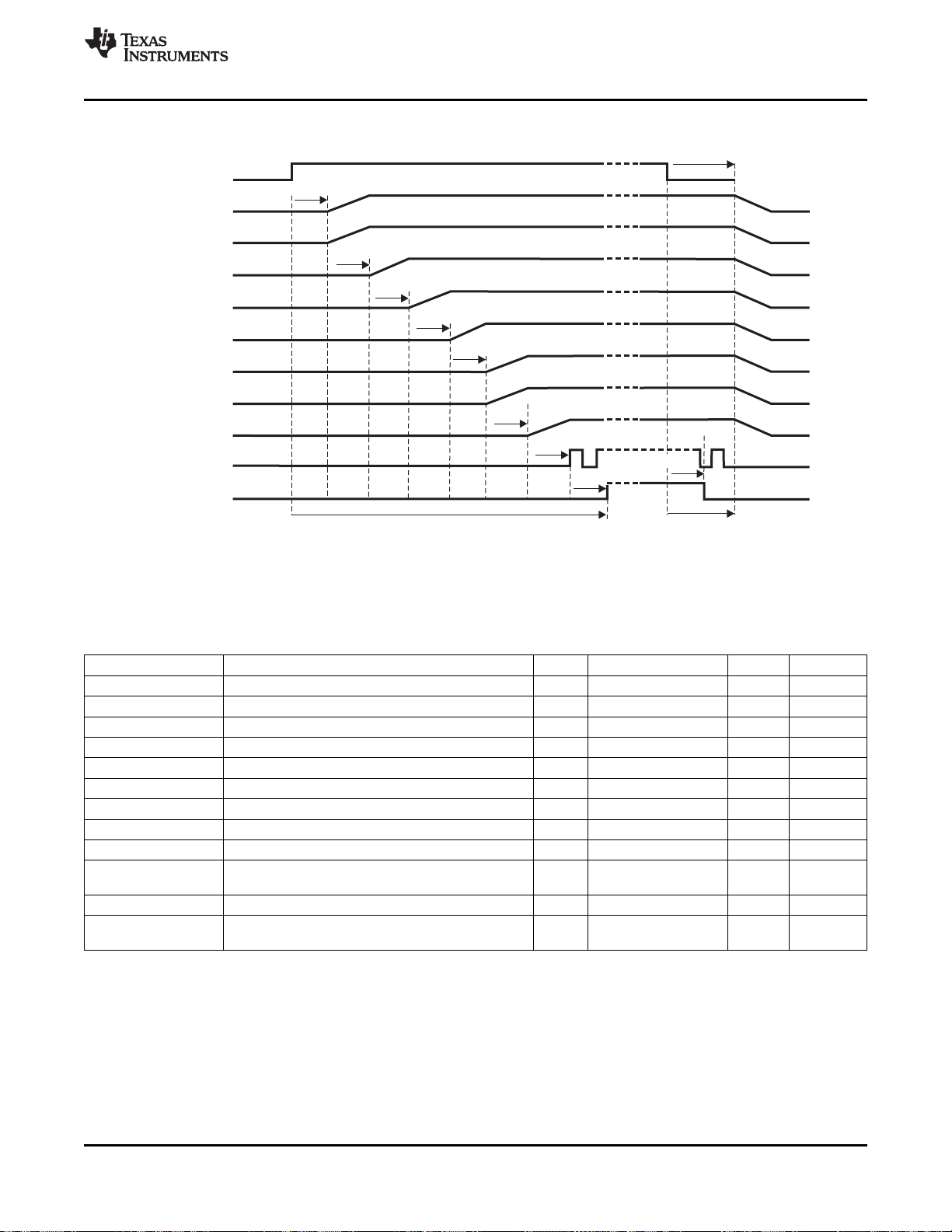
SWCS046-018
PWRHOLD
VIO/VFBIO
VAUX1
VDD2/VFB2
VDD1/VFB1
VPLL
VDAC
VAUX2
VMMC
CLK32KOUT
NRESPWRON
t
dSOFF2
t
dSON1
1.8 V
1.8 V
3.3 V
t
dSON2
t
dSON3
1.2 V
1.8 V
1.8 V
t
dSON4
t
dSON5
1.8 V
t
dSON6
t
dSON7
3.3 V
t
dSON8
t
dSOFF1
Switch-off sequence
t : Switch-on sequence
dSONT
TPS65910, TPS65910A, TPS65910A3, TPS659101, TPS659102, TPS659103
TPS659104, TPS659105, TPS659106, TPS659107, TPS659108, TPS659109
www.ti.com
Figure 2 shows the 00 Boot mode timing characteristics.
SWCS046T –MARCH 2010–REVISED SEPTEMBER 2013
Figure 2. Boot Mode: BOOT1 = 0, BOOT0 = 0
Table 3 lists the 00 Boot mode timing characteristics.
Table 3. Boot Mode: BOOT1 = 0, BOOT0 = 0 Timing Characteristics
PARAMETER TEST CONDITIONS MIN TYP MAX UNIT
t
dSON1
t
dSON2
t
dSON3
t
dSON4
t
dSON5
t
dSON6
t
dSON8
t
dSONT
t
dSOFF1
t
dSOFF1B
t
dSOFF2
PWRHOLD rising edge to VIO, VAUX1 enable delay 66 × t
VIO to VDD2 enable delay 64 × t
VDD2 to VDD1 enable delay 64 × t
VDD1 to VPLL enable delay 64 × t
VPLL to VDAC,VAUX2 enable delay 64 × t
VDAC to VMMC enable delay 64 × t
VMMC to CLK32KOUT rising edge delay 64 × t
CLK32KOUT to NRESPWRON rising edge delay 64 × t
Total switch-on delay 16 ms
PWRHOLD falling edge to NRESPWRON falling edge
delay
2 × t
NRESPWRON falling edge to CLK32KOUT low delay 3 × t
PWRHOLD falling edge to supplies and reference
disable delay
5 × t
= 2060 µs
CK32k
= 2000 µs
CK32k
= 2000 µs
CK32k
= 2000 µs
CK32k
= 2000 µs
CK32k
= 2000 µs
CK32k
= 2000 µs
CK32k
= 2000 µs
CK32k
= 62.5 µs
CK32k
= 92 µs
CK32k
= 154 µs
CK32k
Registers default setting: CK32K_CTRL = 1 (32-kHz RC oscillator is used), RTC_PWDN = 1 (RTC domain off),
IT_POL = 0 (INt2 interrupt flag active low), VMBHI_IT_MSK = 0 (automatic switch-on on Battery plug),
VMBCH_SEL = 11.
BOOT1 = 0, BOOT0 = 1
Table 4 provides details about the EEPROM setting for the BOOT modes. The power-up sequence for this boot
mode is provided in Figure 3.
Copyright © 2010–2013, Texas Instruments Incorporated Submit Documentation Feedback 29
Product Folder Links: TPS65910 TPS65910A TPS65910A3 TPS659101 TPS659102 TPS659103 TPS659104
TPS659105 TPS659106 TPS659107 TPS659108 TPS659109
TPS65910, TPS65910A, TPS65910A3, TPS659101, TPS659102, TPS659103
TPS659104, TPS659105, TPS659106, TPS659107, TPS659108, TPS659109
SWCS046T –MARCH 2010–REVISED SEPTEMBER 2013
Table 4. Fixed Boot Mode: 01
Register Bit Description
VDD1_OP_REG SEL VDD1 voltage level selection for boot 1.2 V
VDD1_REG VGAIN_SEL VDD1 Gain selection, x1 or x2 x1
EEPROM VDD1 time slot selection 3
DCDCCTRL_REG VDD1_PSKIP VDD1 pulse skip mode enable Skip enabled
VDD2_OP_REG/VDD2_SR_REG SEL VDD2 voltage level selection for boot 1.2 V
VDD2_REG VGAIN_SEL VDD2 Gain selection, x1 or x3 x1
EEPROM VDD2 time slot selection 4
DCDCCTRL_REG VDD2_PSKIP VDD2 pulse skip mode enable Skip enabled
VIO_REG SEL VIO voltage selection 1.8 V
EEPROM VIO time slot selection 1
DCDCCTRL_REG VIO_PSKIP VIO pulse skip mode enable Skip enabled
EEPROM VDD3 time slot OFF
VDIG1_REG SEL LDO voltage selection 1.2 V
EEPROM LDO time slot OFF
VDIG2_REG SEL LDO voltage selection 1.0 V
EEPROM LDO time slot OFF
VDAC_REG SEL LDO voltage selection 1.8 V
EEPROM LDO time slot OFF
VPLL_REG SEL LDO voltage selection 1.8 V
EEPROM LDO time slot 2
VAUX1_REG SEL LDO voltage selection 1.8 V
EEPROM LDO time slot OFF
VMMC_REG SEL LDO voltage selection 1.8 V
EEPROM LDO time slot OFF
VAUX33_REG SEL LDO voltage selection 3.3 V
EEPROM LDO time slot 6
VAUX2_REG SEL LDO voltage selection 1.8 V
EEPROM LDO time slot 5
CLK32KOUT pin CLK32KOUT time slot 7
NRESPWRON pin NRESPWRON time slot 7+1
VRTC_REG low-power mode
DEVCTRL_REG RTC_PWDN 1
DEVCTRL_REG CK32K_CTRL Crystal
DEVCTRL2_REG 0: 0.5 ms 2 ms
DEVCTRL2_REG IT_POL Active-low
INT_MSK_REG VMBHI_IT_MSK switch-on from
VMBCH_REG VMBCH_SEL[1:0] 3 V
VRTC_OFFMAS
K
TSLOT_LENGTH
[0]
0: VRTC LDO will be in low-power mode during OFF state
1: VRC LDO will be in full-power mode during OFF state
0: RTC in normal power mode
1: Clock gating of RTC register and logic, low-power mode
0: Clock source is crystal/external clock
1: Clock source is internal RC oscillator
Boot sequence time slot duration:
1: 2 ms
0: INT1 signal will be active-low
1: INT1 signal will be active-high
0: Device will automatically switch-on at NOSUPPLY to
OFF or BACKUP to OFF transition
1: Startup reason required before switch-on
Select threshold for main battery comparator threshold
VMBCH.
www.ti.com
TPS65910
Boot 01
0: Automatic
supply insertion
30 Submit Documentation Feedback Copyright © 2010–2013, Texas Instruments Incorporated
Product Folder Links: TPS65910 TPS65910A TPS65910A3 TPS659101 TPS659102 TPS659103 TPS659104
TPS659105 TPS659106 TPS659107 TPS659108 TPS659109

t
dSON1
1.8 V
t
dSON7
SWCS046-019
t
dSON8
Switch-off sequence
t : Switch-on sequence
dSONT
1.8 V
1.2 V
3.3 V
1.8 V
1.2 V
t
dSON2
t
dSON3
t
dSON4
t
dSON5
t
dSON6
t
dSOFF2
t
dSOFF1
PWRHOLD
VIO/VFBIO
VPLL
VDD2/VFB2
VDD1/VFB1
VAUX2
VAUX33
CLK32KOUT
NRESPWRON
TPS65910, TPS65910A, TPS65910A3, TPS659101, TPS659102, TPS659103
TPS659104, TPS659105, TPS659106, TPS659107, TPS659108, TPS659109
www.ti.com
Figure 3 shows the 01 Boot mode timing characteristics.
SWCS046T –MARCH 2010–REVISED SEPTEMBER 2013
Figure 3. Boot Mode: BOOT1 = 0, BOOT0 = 1
Table 5 lists the 01 Boot mode timing characteristics.
Table 5. Boot Mode: BOOT1 = 0, BOOT0 = 1 Timing Characteristics
PARAMETER TEST CONDITIONS MIN TYP MAX UNIT
t
dSON1
t
dSON2
t
dSON3
t
dSON4
t
dSON5
t
dSON7
t
dSON8
t
dSONT
t
dSOFF1
t
dSOFF1B
t
dSOFF2
Registers default setting: CK32K_CTRL = 0 (32-kHz quartz or external bypass clock is used), RTC_PWDN = 1
PWRHOLD rising edge to VIO enable delay 66 × t
VIO to VPLL enable delay 64 × t
VPLL to VDD1 enable delay 64 × t
VDD1 to VDD2 enable delay 64 × t
VDD2 to VAUX2 enable delay 64 × t
VAUX2 to VAUX33 enable delay 64 × t
VAUX33 to CLK32KOUT enable delay 64 × t
CLK32KOUT to NRESPWRON enable delay 64 × t
= 2060 µs
CK32k
= 2000 µs
CK32k
= 2000 µs
CK32k
= 2000 µs
CK32k
= 2000 µs
CK32k
= 2000 µs
CK32k
= 2000 µs
CK32k
= 2000 µs
CK32k
Total switch-on delay 16 ms
PWRHOLD falling edge to NRESPWRON falling edge 2 × t
NRESPWRON falling edge to CLK32KOUT low delay 3 × t
PWRHOLD falling edge to supplies disable delay 5 × t
= 62.5 µs
CK32k
= 92 µs
CK32k
= 154 µs
CK32k
(RTC domain off), IT_POL = 0 (INt2 interrupt flag active low), VMBHI_IT_MSK = 0 (automatic switch-on on
battery plug), VMBCH_SEL = 11.
POWER CONTROL TIMING
Device Turn-On/Off With Rising/Falling Input Voltage
Figure 4 shows the device turn-on/-off with rising/falling input voltage.
Copyright © 2010–2013, Texas Instruments Incorporated Submit Documentation Feedback 31
Product Folder Links: TPS65910 TPS65910A TPS65910A3 TPS659101 TPS659102 TPS659103 TPS659104
TPS659105 TPS659106 TPS659107 TPS659108 TPS659109

PWRON
VIO
INT1
1.8 V
NRESPWRON
Interrupt acknowledge
PWRHOLD
PWRON_IT=1
CLK33KOUT
Interrupt acknowledge
Switch-off
sequence
t
t
dbPWRONF
t
dSONT
t
dbPWRONF
t
dONPWHOLD
Switch-on sequence
SWCS046-009
PWRON_IT=1
dbPWRHOLDF
t
dOINT1
(1)
SWCS046-022
VCC7
VIO
INT1
1.8V
t
d32KON
NRESPWRON
t
dSONT
Switch-on sequence
Interrupt aknowledge
PWRHOLD
VMBHI_IT=1
t
dONVMBHI
CLK33KOUT
VMBCH threshold
VMBHI threshold
VRTC
1.8V
t
dbVMBHI
VMBDCH threshold
VMBLO threshold
VBNPR threshold
t
dbVMBDCH
t
dbVMBLO
Switch-off sequence
VBACKUP > VBNPR
(1)
t
dOINT1
TPS65910, TPS65910A, TPS65910A3, TPS659101, TPS659102, TPS659103
TPS659104, TPS659105, TPS659106, TPS659107, TPS659108, TPS659109
SWCS046T –MARCH 2010–REVISED SEPTEMBER 2013
POWER CONTROL TIMING (continued)
www.ti.com
NOTE: (1) The DEV_ON control bit (set to 1) or the PWRHOLD signal (set high) can be used to maintain supplies on after
the switch-on sequence. If none of these devce Power On enable conditions is set, the supplies will be turned off after
t
delay.
dOINT1
Figure 4. Device Turn-On/Off with Rising/Falling Input Voltage
Device State Control Through PWRON Signal
Figure 5 shows the device state control through PWRON signal.
NOTE: (1) The DEV_ON control bit (set to 1) or the PWRHOLD signal (set high) can be used to maintain supplies on after
switch-on sequence, If none of these device POWER ON enable condition is set the supplies will be turned off after
T
delay.
dOINT1
Figure 6 shows the long-press turn-off timing characteristics.
Figure 5. PWRON Turn-On/Turn-Off
32 Submit Documentation Feedback Copyright © 2010–2013, Texas Instruments Incorporated
Product Folder Links: TPS65910 TPS65910A TPS65910A3 TPS659101 TPS659102 TPS659103 TPS659104
TPS659105 TPS659106 TPS659107 TPS659108 TPS659109
PWRON
VIO
INT1
NRESPWRON
PWRHOLD
PWRON_LP_IT=1
PWRON_IT=1
Switch-off
sequence
t
dPWRONLPTO
t
dPWRONLP
t
dbPWRONF
SWCS046-010
PWRON_IT=1
TPS65910, TPS65910A, TPS65910A3, TPS659101, TPS659102, TPS659103
TPS659104, TPS659105, TPS659106, TPS659107, TPS659108, TPS659109
www.ti.com
POWER CONTROL TIMING (continued)
NOTE: If the DEV_ON control bit is set to 1 or PWRHOLD is kept high, the device will be turned on again after PWRON long
press turn-off and PWRON released.
Figure 6. PWRON Long-Press Turn-Off
SWCS046T –MARCH 2010–REVISED SEPTEMBER 2013
Table 6 lists the power control timing characteristics.
Table 6. Power Control Timing Characteristics
PARAMETER TEST CONDITIONS MIN TYP MAX UNIT
BOOT[1:0] = 00, RC oscillator 0.1
t
: 32-kHz Oscillator turn-on time 400 2000 ms
d32KON
t
: VMBHI rising-edge debouncing delay t
dbVMBHI
t
dbVMBDCH
falling-edge delay = 125
t
dbVMBLO
NRESPWRON falling-edge delay = 125
t
dbPWRONF
t
dbPWRONR
t
dbPWRHOLD
t
dOINT
low-level (debounced) event
t
dONPWHOLD
control bit after NRESPWRON released to keep on the supplies
t
dPWRONLP
t
dPWRONLPTO
: Main Battery voltage = VMBDCH threshold to INT1 4 × t
: Main Battery voltage = VMBLO threshold to 4 × t
: PWRON falling-edge debouncing delay 500 550 ms
: PWRON rising-edge debouncing delay t
: PWRON rising-edge debouncing delay t
: INT1 (internal) Power-on pulse duration after PWRON
: delay to set high PWRHOLD signal or DEV_ON
: PWRON long-press delay to interrupt 6 s
: PWRON long-press delay to turn-off 8 s
BOOT[1:0] = 01, Quartz
oscillator
BOOT[1:0] = 01, Bypass clock 0.1
3 ×
= µs
CK32k
94
3 ×
t
= s
CK32k
94
3 ×
t
= s
CK32k
94
3 ×
= µs
CK32k
94
2 × 3 ×
= t
CK32k
63 94
984 ms
PWRON falling edge to
PWON_LP_IT = 1
PWRON falling edge to
NRESPWRON falling edge
4 × t
= 125
4 × t
= 125
CK32k
1 s
CK32k
CK32k
CK32k
CK32k
= µs
Copyright © 2010–2013, Texas Instruments Incorporated Submit Documentation Feedback 33
Product Folder Links: TPS65910 TPS65910A TPS65910A3 TPS659101 TPS659102 TPS659103 TPS659104
TPS659105 TPS659106 TPS659107 TPS659108 TPS659109
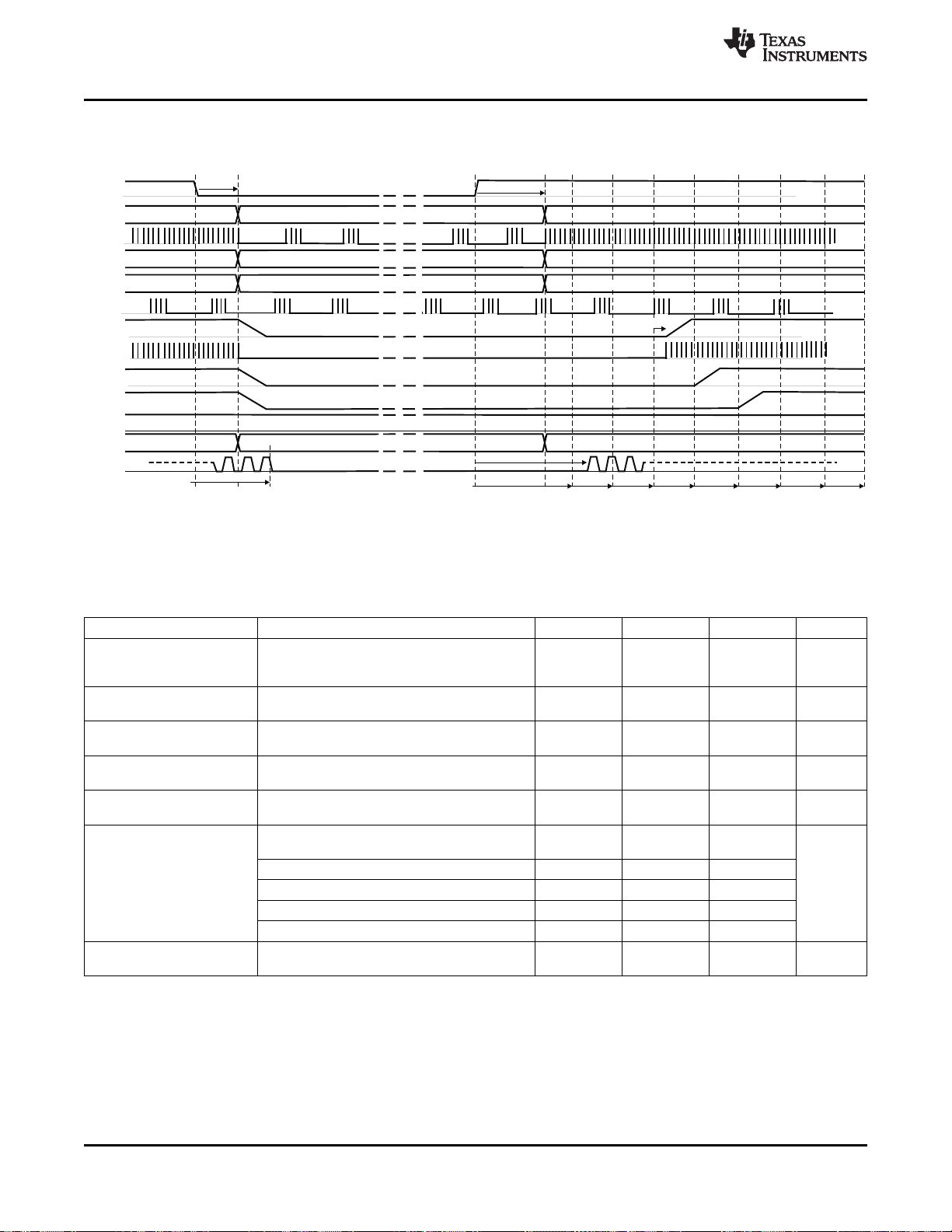
SWCS046-024
SLEEP
t
ACT2SLP
VIO/VFBIO 1.8 V
PWM mode
VAUX1
VDD2/VFB2
VDD1/VFB1
VPLL
VDAC
VAUX2
VMMC
CLK32KOUT
SWIO
SW2
SW1
1.8 V
Low-power mode
1.8 V
PWM mode
1.8 V
Active mode
1.8 V
Low-power mode
1.8 V
Active mode
3.3 V
Pulse skip mode
3.3 V
Low-power mode
3.3 V
1.2 V
PWM mode
Off
1.8 V
Active mode
1.8 V
Active mode
1.8 V
Active mode
3.3 V
Active mode
3.3 V
Low-power mode
Off
Off
1.8 V
Active mode
1.8 V
Active mode
3.3 V
Active mode
1.2 V
PWM mode
1.8 V
Active mode
1.8 V
Active mode
t
SLP2ACT
t
SLP2ACTCK32K
t
dSLPON1
t
dSLPONST
t
dSLPONST
t
dONDCDCSLP
t
ACT2SLPCK32K
Pulse skip mode
TPS65910, TPS65910A, TPS65910A3, TPS659101, TPS659102, TPS659103
TPS659104, TPS659105, TPS659106, TPS659107, TPS659108, TPS659109
SWCS046T –MARCH 2010–REVISED SEPTEMBER 2013
Device SLEEP State Control
Figure 7 shows the device SLEEP state control timing characteristics.
www.ti.com
NOTE: Registers programming: VIO_PSKIP = 0, VDD1_PSKIP = 0, VDD1_SETOFF = 1, VDAC_SETOFF = 1,
VPLL_SETOFF = 1, VAUX2_KEEPON = 1
Figure 7. Device SLEEP State Control
Table 7. Device SLEEP State Control Timing Characteristics
PARAMETER TEST CONDITIONS MIN TYP MAX UNIT
t
ACT2SLP
t
ACT2SLP
t
SLP2ACT
t
SLP2ACTCK32K
t
dSLPON1
mode µs
(SLEEP resynchronization delay)
SLEEP falling edge to CLK32KOUT low 156 188 µs
SLEEP rising edge to supply in high power 8 × t
mode 250 281
SLEEP rising edge to CLK32KOUT running 344 375 µs
SLEEP rising edge to time step 1 of the tun-on t
sequence from SLEEP state t
turn-on sequence step duration, from SLEEP
state
TSLOT_LENGTH[1:0] = 00 0
t
SLEEP falling edge to supply in low power
dSLPONST
t
dSLPONDCDC
34 Submit Documentation Feedback Copyright © 2010–2013, Texas Instruments Incorporated
Product Folder Links: TPS65910 TPS65910A TPS65910A3 TPS659101 TPS659102 TPS659103 TPS659104
TSLOT_LENGTH[1:0] = 01 200
TSLOT_LENGTH[1:0] = 10 500
TSLOT_LENGTH[1:0] = 11 2000
VDD1, VDD2 or VIO tun-on delay from tun-on 2 × t
sequence time step 62
TPS659105 TPS659106 TPS659107 TPS659108 TPS659109
2 × t
= 3 × t
CK32k
62 94
t
= 9 × t
CK32k
t
281 312 µs
ACT2SLP
t
CK32k
SLP2ACT
t
CK32k
SLP2ACT
CK32k
CK32k
+ 3 ×
+ 3 ×
+ 1 ×
=
CK32k
CK32k
=
=
µs
µs
us
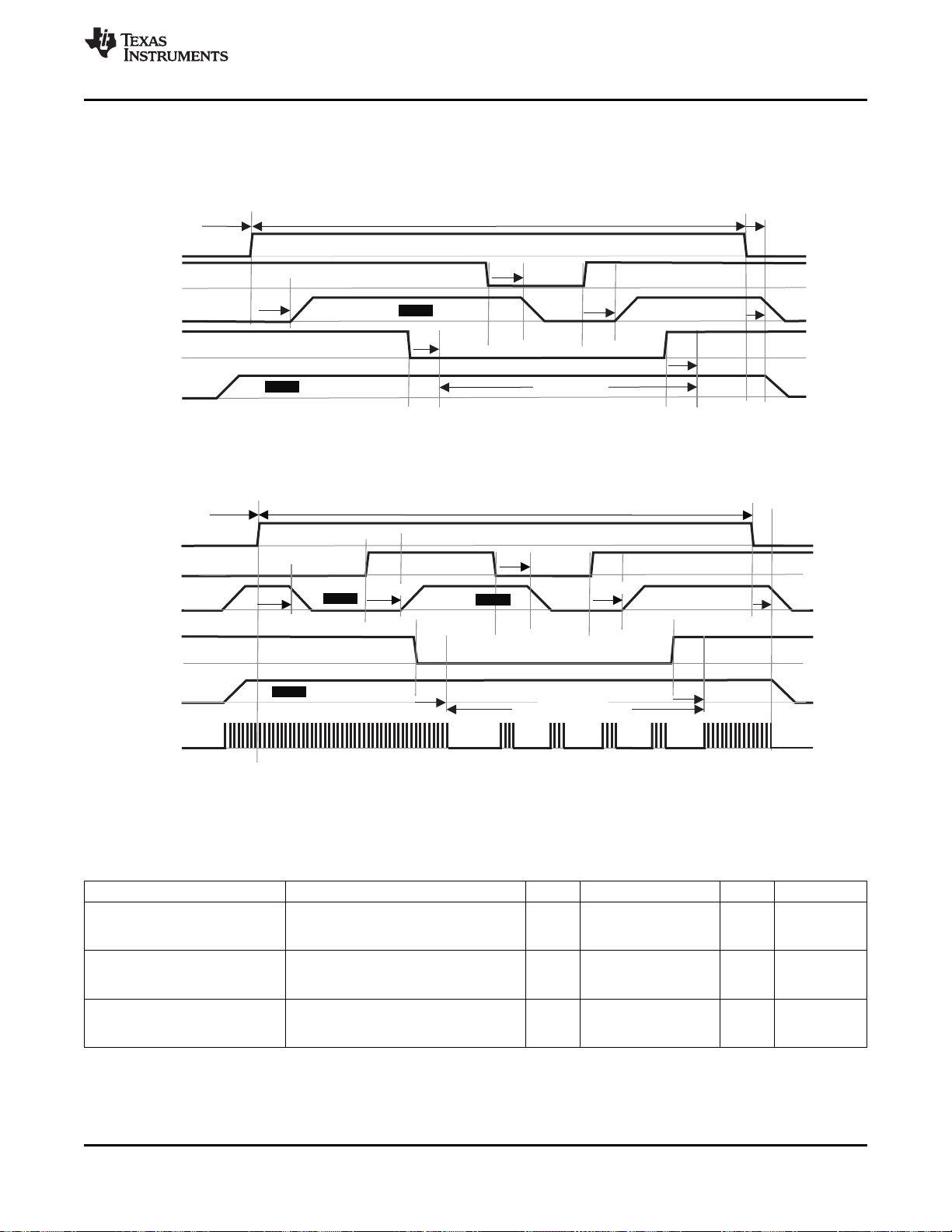
SWCS046-017
SCLSR_EN2
VDD2/VFB2
VDD1/VFB1
1.2 V
SCLSR_EN1
NRESPWRON
Low-power mode
PFM (pulse skipping) mode
Switch-on sequence
Switch-off sequence
Device on
PWM mode
SW1
t
dOEN
0 V
t
dVDDEN
t
dEN
3.3 V
t
dVDDEN
t
dSOFF2
t
dEN
t
dEN
SWCS046-016
SCLSR_EN1
VDIG1
1.2 V
VPLL
1.8 V
SCLSR_EN2
NRESPWRON
t
dVEN
t
dEN
Switch-on sequence Switch-off sequence
Device on
t
dEN
t
dEN
t
dSOFF2
t
dEN
Low-power mode
TPS65910, TPS65910A, TPS65910A3, TPS659101, TPS659102, TPS659103
TPS659104, TPS659105, TPS659106, TPS659107, TPS659108, TPS659109
www.ti.com
Power Supplies State Control Through the SCLSR_EN1 and SDASR_EN2 Signals
Figure 8 andFigure 9 show the power supplies state control through the SCLSR_EN1 and SDASR_EN2 signals
timing characteristics.
NOTE: Register setting: VDIG1_EN1 = 1, VPLL_EN2 = 1, and VPLL_KEEPON = 1
Figure 8. LDO Type Supplies State Control Through SCLSR_EN1 and SCLSR_EN2
SWCS046T –MARCH 2010–REVISED SEPTEMBER 2013
NOTE: Register setting: VDD2_EN2 = 1, VDD1_EN1 = 1, VDD1_KEEPON = 1, VDD1_PSKIP = 0, and SEL[6:0] = hex00 in
VDD2_SR_REG
Figure 9. VDD1 and VDD2 Supplies State Control Through SCLSR_EN1 and SCLSR_EN2
Table 8. Supplies State Control Though SCLSR_EN1 and SCLSR_EN2 Timing Characteristics
PARAMETER TEST CONDITIONS MIN TYP MAX UNIT
t
: NREPSWON to supply state
dEN
change delay, SCLSR_EN1 or 0 ms
SCLSR_EN2 driven
t
: SCLSR_EN1 or
dEN
SCLSR_EN2 edge to supply state 1 × t
change delay
t
: SCLSR_EN1 or
dVDDEN
SCLSR_EN2 edge to VDD1 or 3 × t
VDD2 dc-dc turn on delay
Copyright © 2010–2013, Texas Instruments Incorporated Submit Documentation Feedback 35
Product Folder Links: TPS65910 TPS65910A TPS65910A3 TPS659101 TPS659102 TPS659103 TPS659104
TPS659105 TPS659106 TPS659107 TPS659108 TPS659109
= 31 µs
CK32k
= 63 µs
CK32k
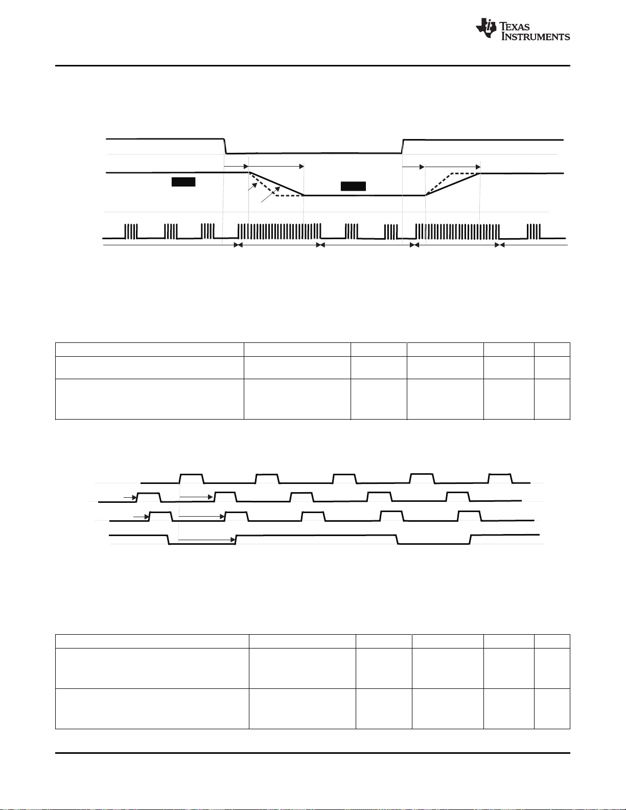
SWCS046-025
SW3
SW2
SWIO
SW1
t
dswio2sw1
t
dswio2sw2
t
dswio2sw3
t
dviosync
1.2 V
SCLSR_EN2
PFM (pulse
skipping) mode
SW1
VDD1/VFB1
0.8 V
PFM (pulse
skipping) mode
PFM (pulse skipping) mode
PWM mode PWM mode
t
dDVSEN
t
dDVSENL
t
dDVSEN
TSTEP[2:0]=001
TSTEP[2:0]=011
t
dDVSENL
SWCS046-021
TPS65910, TPS65910A, TPS65910A3, TPS659101, TPS659102, TPS659103
TPS659104, TPS659105, TPS659106, TPS659107, TPS659108, TPS659109
SWCS046T –MARCH 2010–REVISED SEPTEMBER 2013
VDD1 and VDD2 Voltage Control Through SCLSR_EN1 and SDASR_EN2 Signals
Figure 10 shows the VDD1 and VDD2 voltage control through the SCLSR_EN1 and SDASR_EN2 signals timing
characteristics.
NOTE: Register setting: VDD1_EN1 = 1, SEL[6:0] = hex13 in VDD1_SR_REG
Figure 10. VDD1 Supply Voltage Control Though SCLSR_EN1
www.ti.com
Table 9. VDD1 Supply Voltage Control Through SCLSR_EN1 Timing Characteristics
PARAMETER TEST CONDITIONS MIN TYP MAX UNIT
t
: SCLSR_EN1 or SCLSR_EN2 edge to
dDVSEN
VDD1 or VDD2 voltage change delay
t
: VDD1 or VDD2 voltage settling delay TSTEP[2:0] = 001 32 µs
dDVSENL
2 × t
= 62 µs
CK32k
TSTEP[2:0] = 011 (default) 0.4/7.5 = 53
TSTEP[2:0] = 111 160
SMPS Switching Synchronization
Figure 11 shows the SMPS switching synchronization timing characteristics.
NOTE: VDD1 or VDD2 switching synchronization is available in PWM mode (VDD1_PSKIP = 0 or VDD2_PSKIP = 0). SMPS
external clock (GPIO_CKSYNC) synchronization is available when VIO PWM mode is set (VIO_PSKIP = 0).
Figure 11. SMPS Switching Synchronization
Table 10. SMPS Switching Synchronization Timing Characteristics
PARAMETER TEST CONDITIONS MIN TYP MAX UNIT
t
dSWIO2SW1
rising edge
t
dSWIO2SW2
rising edge
: delay from SWIO rising edge to SW1
: delay from SWIO rising edge to SW1
36 Submit Documentation Feedback Copyright © 2010–2013, Texas Instruments Incorporated
Product Folder Links: TPS65910 TPS65910A TPS65910A3 TPS659101 TPS659102 TPS659103 TPS659104
TPS659105 TPS659106 TPS659107 TPS659108 TPS659109
VDD1_PSKIP = 0,
DCDCCKSYNC[1:0] = 11 160 ns
DCDCCKSYNC[1:0] = 01 220
VDD2_PSKIP = 0,
DCDCCKSYNC[1:0] = 11 160 ns
DCDCCKSYNC[1:0] = 01 290

www.ti.com
t
dSWIO2SW3
rising edge
TPS65910, TPS65910A, TPS65910A3, TPS659101, TPS659102, TPS659103
TPS659104, TPS659105, TPS659106, TPS659107, TPS659108, TPS659109
SWCS046T –MARCH 2010–REVISED SEPTEMBER 2013
Table 10. SMPS Switching Synchronization Timing Characteristics (continued)
PARAMETER TEST CONDITIONS MIN TYP MAX UNIT
: delay from SWIO rising edge to SW3
206 ns
Copyright © 2010–2013, Texas Instruments Incorporated Submit Documentation Feedback 37
Product Folder Links: TPS65910 TPS65910A TPS65910A3 TPS659101 TPS659102 TPS659103 TPS659104
TPS659105 TPS659106 TPS659107 TPS659108 TPS659109

TPS65910, TPS65910A, TPS65910A3, TPS659101, TPS659102, TPS659103
TPS659104, TPS659105, TPS659106, TPS659107, TPS659108, TPS659109
SWCS046T –MARCH 2010–REVISED SEPTEMBER 2013
DEVICE INFORMATION
Table 11. Terminal Functions
NAME QFN PIN SUPPLIES TYPE I/O DESCRIPTION PU/PD
VDDIO VDDIO/DGND Power I Digital I/Os supply No
SDA_SDI VDDIO/DGND Digital I/O peripheral interface data input External PU
SCL_SCK VDDIO/DGND Digital I/O peripheral interface Clock Input External PU
SDASR_EN2 VDDIO/DGND Digital I/O External PU
SCLSR_EN1 VDDIO/DGND Digital I/O External PU
SLEEP VDDIO/DGND Digital I
GPIO_CKSYNC VDDIO/DGND Digital I/O DC-DCs synchronization clock input
PWRHOLD VRTC/DGND Digital I Switch-on/-off control signal
PWRON VBAT/DGND Digital I External switch-on control (ON button)
NRESPWRON VDDIO/DGND Digital O Power off reset
INT1 VDDIO/DGND Digital O Interrupt flag No
BOOT0 VRTC/DGND Digital I Power-up sequence selection
BOOT1 VRTC/DGND Digital I Power-up sequence selection
CLK32KOUT VDDIO/DGND Digital O 32-kHz clock output ACTIVE or SLEEP
OSC32KIN VRTC/REFGND Analog I 32-kHz crystal oscillator No
OSC32KOUT VRTC/REFGND Analog I 32-kHz crystal oscillator No
VREF VCC7/REFGND Analog O Bandgap voltage No
REFGND REFGND Analog I/O Reference ground No
TESTV VCC7/AGND Analog O Analog test output (DFT) No
VBACKUP VBACKUP/AGND Power I No
VCC1 VCC1/GND1 Power I VDD1 dc-dc power input No
GND1 VCC1/GND1 Power I/O VDD1 dc-dc power ground No
SW1 VCC1/GND1 Power O VDD1 dc-dc switched output No
VFB1 VCC7/AGND Analog I VDD1 feedback voltage PD
VCC2 VCC2/GND2 Power I VDD2 dc-dc power input No
GND2 VCC2/GND2 Power I/O VDD2 dc-dc power ground No
SW2 VCC2/GND2 Power O VDD2 dc-dc switched output No
VFB2 VCC4/AGND2 Analog I VDD2 dc-dc feedback voltage PD
VCCIO VCCIO/GNDIO Power I VIO dc-dc power input No
GNDIO VCCIO/GNDIO Power I/O VIO dc-dc power ground No
SWIO VCCIO/GNDIO Power O VIO dc-dc switched output No
VFBIO VCC7/AGND Analog I VIO feedback voltage PD
VCC3 VCC3/AGND2 Power I VMMC VAUX33 power input No
VMMC VCC3/REFGND Power O LDO regulator output PD
I2C bidirectional data signal/serial
(multiplexed)
I2C bidirectional clock signal/serial
(multiplexed)
I2C SmartReflex bidirectional data
signal/enable of supplies (multiplexed)
I2C SmartReflex bidirectional clock
signal/enable of supplies (multiplexed)
Active-sleep state transition control Programmable PD
signal (default active)
Configurable general-purpose I/O or
signal
Backup battery input (short to VCC5 if
not used)
Programmable PD
Programmable PD
Programmable PU
Programmable PD
Programmable PD
www.ti.com
(default active)
(default active)
(default active)
PD active during
device OFF state
(default active)
(default active)
PD disable in
state
38 Submit Documentation Feedback Copyright © 2010–2013, Texas Instruments Incorporated
Product Folder Links: TPS65910 TPS65910A TPS65910A3 TPS659101 TPS659102 TPS659103 TPS659104
TPS659105 TPS659106 TPS659107 TPS659108 TPS659109

TPS65910, TPS65910A, TPS65910A3, TPS659101, TPS659102, TPS659103
TPS659104, TPS659105, TPS659106, TPS659107, TPS659108, TPS659109
www.ti.com
Table 11. Terminal Functions (continued)
NAME QFN PIN SUPPLIES TYPE I/O DESCRIPTION PU/PD
VAUX33 VCC3/REFGND Power O PD
VCC4 VCC4/AGND2 Power I VAUX1, VAUX2 power input No
VAUX1 VCC4/REFGND Power O LDO regulator output PD
VAUX2 VCC4/REFGND Power O LDO regulator output PD
VCC5 VCC5/AGND Power I VDAC, VPLL power input No
VDAC VCC5/REFGND Power O LDO regulator output PD
VPLL VCC5/REFGND Power O LDO regulator output PD
VRTC VCC7/REFGND Power O LDO regulator output PD
VCC6 VCC6/AGND2 Power I VDIG1, VDIG2 power input No
VDIG1 VCC6/REFGND Power O LDO regulator output No
VDIG2 VCC6/REFGND Power O LDO regulator output No
VCC7 VCC7/REFGND Power I No
VFB3 VCC7/AGND Analog I VDD3 feedback voltage No
SW3 VCC7/GND3 Power O VDD3 dc-dc switched output No
GND3 AGND Power I/O VDD3 dc-dc power ground No
AGND AGND Power I/O Analog ground No
AGND2 AGND Power I/O Analog ground No
DGND DGND Power I/O Digital ground No
Power
PAD
Power
PAD
Power
PAD
Power
PAD
LDO regulator output, VDD3 internal
regulated supply
VRTC power input, VDD3 internal and
analog references supply
SWCS046T –MARCH 2010–REVISED SEPTEMBER 2013
Copyright © 2010–2013, Texas Instruments Incorporated Submit Documentation Feedback 39
Product Folder Links: TPS65910 TPS65910A TPS65910A3 TPS659101 TPS659102 TPS659103 TPS659104
TPS659105 TPS659106 TPS659107 TPS659108 TPS659109
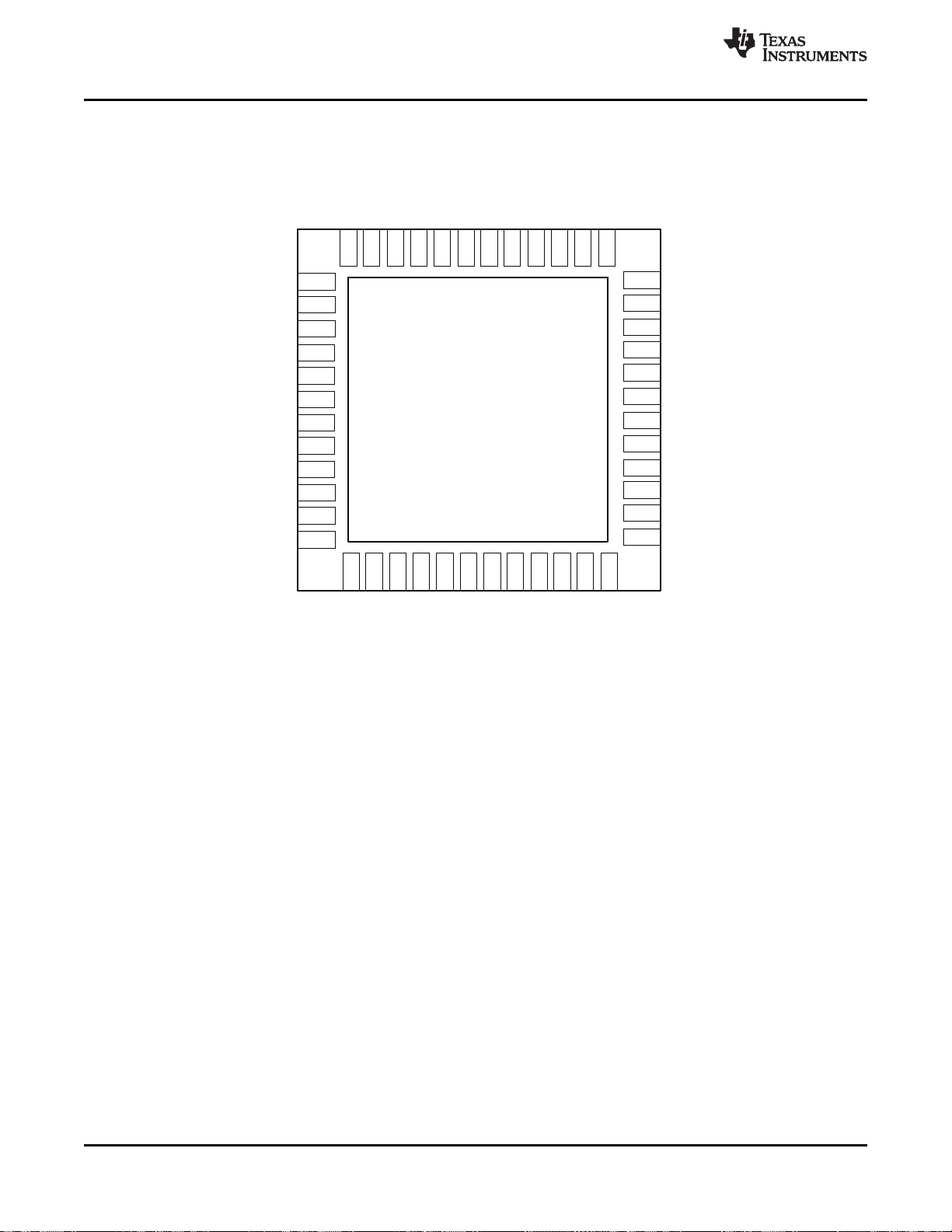
1
2
3
4
5
6
7
8
9
SLEEP
37
CLK32KOUT
38
GPIO/CKSYN
39
NRESPWRON
40
VCC2
41
SW2
42
GND2
43
VFB2
44
INT1
45
VAUX1
46
VCC4
47
VAUX2
48
24 VPLL
23 VCC5
22 VDAC
21 OSC32KOUT
20 OSC32KIN
19 BOOT1
18 VREF
17 REFGND
16 VFBIO
15 GNDIO
14 SWIO
13 VCCIO
PowerPad
VCC1
SW1
GND1
PWRON
VFB1
SW3
VFB3
VRRTC
VCC7
VBACKUP
BOOT0
TESTV
36
35
34
33
32
31
30
29
28
27
26
25
10
11
12
PWRHOLD
VMMC
VCC3
VAUX33
VDIG2
VCC6
VDIG1
SDA
SCL
SDASR/EN2
SCLSR/EN1
VDDIO
SWCS046-004
TPS65910, TPS65910A, TPS65910A3, TPS659101, TPS659102, TPS659103
TPS659104, TPS659105, TPS659106, TPS659107, TPS659108, TPS659109
SWCS046T –MARCH 2010–REVISED SEPTEMBER 2013
PIN ASSIGNMENT (TOP VIEW)
www.ti.com
Figure 12. 48-QFN Top View Pin Assignment
TPS659105 TPS659106 TPS659107 TPS659108 TPS659109
40 Submit Documentation Feedback Copyright © 2010–2013, Texas Instruments Incorporated
Product Folder Links: TPS65910 TPS65910A TPS65910A3 TPS659101 TPS659102 TPS659103 TPS659104

TPS65910, TPS65910A, TPS65910A3, TPS659101, TPS659102, TPS659103
TPS659104, TPS659105, TPS659106, TPS659107, TPS659108, TPS659109
www.ti.com
DETAILED DESCRIPTION
POWER REFERENCE
The bandgap voltage reference is filtered by using an external capacitor connected across the VREF output and
the analog ground REFGND (see RECOMMENDED OPERATING CONDITIONS, Recommended Operating
Conditions). The VREF voltage is distributed and buffered inside the device.
POWER SOURCES
The power resources provided by the TPS65910 device include inductor-based switched mode power supplies
(SMPS) and linear low drop-out voltage regulators (LDOs). These supply resources provide the required power
to the external processor cores and external components, and to modules embedded in the TPS65910 device.
Two of these SMPS have DVS capability SmartReflex Class 3 compatible. These SMPS provide independent
core voltage domains to the host processor. The remaining SMPS provides supply voltage for the host processor
I/Os.
Table 12 lists the power sources provided by the TPS65910 device.
Table 12. Power Sources
RESOURCE TYPE VOLTAGES POWER
VIO SMPS 1.5 V / 1.8 V / 2.5 V / 3.3 V 1000 mA
VDD1 SMPS 0.6 ... 1.5 in 12.5-mV steps 1500 mA
Programmable multiplication factor: x2, x3
VDD2 SMPS 0.6 ... 1.5 in 12.5-mV steps 1500 mA
Programmable multiplication factor: x2, x3
VDD3 SMPS 5 V 100 mA
VDIG1 LDO 1.2 V, 1.5 V, 1.8 V, 2.7 V 300 mA
VDIG2 LDO 1 V, 1.1 V, 1.2 V, 1.8 V 300 mA
VPLL LDO 1.0 V, 1.1 V, 1.8 V, 2.5 V 50 mA
VDAC LDO 1.8 V, 2.6 V, 2.8 V, 2.85 V 150 mA
VAUX1 LDO 1.8 V, 2.5 V, 2.8 V, 2.85 V 300 mA
VAUX2 LDO 1.8 V, 2.8 V, 2.9 V, 3.3 V 150 mA
VAUX33 LDO 1.8 V, 2.0 V, 2.8 V, 3.3 V 150 mA
VMMC LDO 1.8 V, 2.8 V, 3.0 V, 3.3 V 300 mA
SWCS046T –MARCH 2010–REVISED SEPTEMBER 2013
EMBEDED POWER CONTROLLER
The embedded power controller manages the state of the device and controls the power-up sequence.
STATE-MACHINE
The EPC supports the following states:
No supply: The main battery supply voltage is not high enough to power the VRTC regulator. A global reset is
asserted in this case. Everything on the device is off.
Backup: The main battery supply voltage is high enough to enable the VRTC domain but not enough to switch
on all the resources. In this state, the VRTC regulator is in backup mode and only the 32-K oscillator and RTC
module are operating (if enabled). All other resources are off or under reset.
Off: The main battery supply voltage is high enough to start the power-up sequence but device power on is not
enabled. All power supplies are in OFF state except VRTC.
Active: Device power-on enable conditions are met and regulated power supplies are on or can be enabled with
full current capability.
Sleep: Device SLEEP enable conditions are met and some selected regulated power supplies are in low-power
mode.
Copyright © 2010–2013, Texas Instruments Incorporated Submit Documentation Feedback 41
Product Folder Links: TPS65910 TPS65910A TPS65910A3 TPS659101 TPS659102 TPS659103 TPS659104
TPS659105 TPS659106 TPS659107 TPS659108 TPS659109

NO SUPPLY
OFF
ACTIVE
SLEEP
Backup
MB or BB>VBNPR and
MB<VMBLO
MB and BB<VBNPR
MB<VMBLO
MB>VMBHI
POWER ON
enabled and
MB>VMBCH
MB>VMBHI
POWER ON
disabled
MB and BB<VBNPR
MB and BB<VBNPR
SLEEP
enabled
POWER ON
disabled
MB: Main battery voltage
BB: Backup battery voltage
MB<VMBLO
SLEEP
disabled
MB<VMBLO
SWCS046-011
PWRHOLD
DEV_ON
PWRON
INT1
PWRON_LP_IT
THERM_TS
DEV_OFF
DEV_OFF_RST
POWER ON
enable
SLEEP
DEV_SLP
INT1
SLEEP
enable
SLEEPSIG_POL
NRESPWRON
t
DOINT
Pulse
generator
t
D
TPS65910, TPS65910A, TPS65910A3, TPS659101, TPS659102, TPS659103
TPS659104, TPS659105, TPS659106, TPS659107, TPS659108, TPS659109
SWCS046T –MARCH 2010–REVISED SEPTEMBER 2013
Figure 13 shows the transitions of the state-machine.
www.ti.com
Device power-on enable conditions:
If none of the device power-on disable conditions is met, the following conditions are available to turn on
and/or maintain the ON state of the device:
• PWRON signal low level.
• Or PWRHOLD signal high level.
• Or DEV_ON control bit set to 1 (default inactive).
42 Submit Documentation Feedback Copyright © 2010–2013, Texas Instruments Incorporated
Figure 13. Embebded Power Control State-Machine
Product Folder Links: TPS65910 TPS65910A TPS65910A3 TPS659101 TPS659102 TPS659103 TPS659104
TPS659105 TPS659106 TPS659107 TPS659108 TPS659109

TPS65910, TPS65910A, TPS65910A3, TPS659101, TPS659102, TPS659103
TPS659104, TPS659105, TPS659106, TPS659107, TPS659108, TPS659109
www.ti.com
• Or interrupt flag active (default INT1 low) while the device is off (NRESPWRON = 0) generates a poweron enable condition during a fixed delay (T
pulse duration defined in POWER CONTROL TIMING,
DOINT1
Power Control Timing).
The power-on enable condition pulse occurs only if the interrupt status bit is initially low (no previous
identical interrupt pending in the status register).
The Interrupt sources expected when the device is off are:
• PWRON low-level interrupt (PWRON_IT = 1 in INT_STS_REG register)
• PWRHOLD rising-edge interrupt (PWRHOLD_IT = 1 in INT_STS_REG register)
The Interrupt sources expected if enabled when the device is off are:
• RTC Alarm interrupt (RTC_ALARM_IT = 1 or RTC_PERIOD_IT = 1 in INT_STS_REG register)
• First-time input voltage rising above VMBHI threshold (Boot mode or EEPROM dependent) and input
voltage > VMBCH threshold (VMBCH_IT = 1 in INT_STS_REG register).
GPIO_CKSYNC cannot be used to turn on the device (OFF-to-ACTIVE state transition), even if its associated
interrupt is not masked, but can be used as an interrupt source to wake up the device from SLEEP-to-ACTIVE
state.
Device power-on disable conditions:
• PWRON signal low level during more than the long-press delay: t
programming). The interrupt corresponding to this condtion is PWRON_LP_IT in the INT_STS_REG register.
• Or Die temperature has reached the thermal shutdown threshold.
• Or DEV_OFF or DEV_OFF_RST control bit set to 1 (value of DEV_OFF is cleared when the device is in OFF
state).
Device SLEEP enable conditions:
• SLEEP signal low level (default, or high level depending on the programmed polarity)
• And DEV_SLP control bit set to 1
• And interrupt flag inactive (default INT1 high): no nonmasked interrupt pending
The SLEEP state can be controlled by programming DEV_SLP and keeping the SLEEP signal in the active
polarity state, or it can be controlled through the SLEEP signal setting the DEV_SLP bit to 1 once, after device
turn-on.
SWCS046T –MARCH 2010–REVISED SEPTEMBER 2013
dPWRONLP
(can be disabled though register
SWITCH-ON/-OFF SEQUENCES
The power sequence is the automated switching on of the device resources when an off-to-active transition takes
place.
The device supports three embedded power sequences selectable by the device BOOT pins.
BOOT0 BOOT1 Processor Supported
0 0 AM3517, AM3505
1 0 OMAP3 Family, AM3715/03, DM3730/25
0 1 EEPROM sequence
Details of the boot sequence timing are given in SWITCH-ON/-OFF SEQUENCES AND TIMING. EEPROM
sequences can be used for specific power up sequence for corresponding application processor. For details of
EEPROM sequence refer to the user guides on the product folder:
http://focus.ti.com/docs/prod/folders/print/tps65910.html.
CONTROL SIGNALS
SLEEP
When none of the device sleep-disable conditions are met, a falling edge (default, or rising edge, depending on
the programmed polarity) of this signal causes an ACTIVE-to-SLEEP state transition of the device. A rising edge
(default, or falling edge, depending on the programmed polarity) causes a transition back to ACTIVE state. This
input signal is level sensitive and no debouncing is applied.
Copyright © 2010–2013, Texas Instruments Incorporated Submit Documentation Feedback 43
Product Folder Links: TPS65910 TPS65910A TPS65910A3 TPS659101 TPS659102 TPS659103 TPS659104
TPS659105 TPS659106 TPS659107 TPS659108 TPS659109

TPS65910, TPS65910A, TPS65910A3, TPS659101, TPS659102, TPS659103
TPS659104, TPS659105, TPS659106, TPS659107, TPS659108, TPS659109
SWCS046T –MARCH 2010–REVISED SEPTEMBER 2013
While the device is in SLEEP state, predefined resources are automatically set in their low-power mode or off.
Resources can be kept in their active mode: (full-load capability), programming the SLEEP_KEEP_LDO_ON and
the SLEEP_KEEP_RES_ON registers. These registers contain 1 bit per power resource. If the bit is set to 1,
then that resource stays in active mode when the device is in SLEEP state. 32KCLKOUT is also included in the
SLEEP_KEEP_RES_ON register and the 32-kHz clock output is maintained in SLEEP state if the corresponding
mask bit is set.
PWRHOLD
When none of the device power-on disable conditions are met, a rising edge of this signal causes an OFF-toACTIVE state transition of the device and a falling edge causes a transition back to OFF state. Typically, this
signal is used to control the device in a slave configuration. It can be connected to the SYSEN output signal from
other TPS659xx devices, or the NRESPWRON signal of another TPS65910 device. This input signal is level
sensitive and no debouncing is applied.
A rising edge of PWRHOLD is highlighted though an associated interrupt.
BOOT0/BOOT1
These signals determine which processor the device is working with and hence which power-up sequence is
needed. See SWITCH-ON/-OFF SEQUENCES AND TIMING for more details. There is no debouncing on this
input signal.
NRESPWRON
This signal is used as the reset to the processor. It is held low until the ACTIVE state is reached. See POWER
CONTROL TIMING to get detailed timing.
www.ti.com
CLK32KOUT
This signal is the output of the 32K oscillator, which can be enabled or not during the power-on sequence,
depending on the Boot mode. It can be enabled and disabled by register bit, during ACTIVE state of the device.
CLK32KOUT output can also be enabled or not during SLEEP state of the device depending on the
SLEEPMASK register programming.
PWRON
A falling edge on this signal causes after t
dbPWRONF
debouncing delay (defined in Figure 5 and Table 6) an OFFto-ACTIVE state or SLEEP-to-ACTIVE state transition of the device and makes the corresponding interrupt
(PWRON_IT) active. The PWRON input is connected to an external push-button. The built-in debouncing time
defines a minimum button press duration that is required for button press detection. Any button press duration
which is lower than this value is ignored, considered an accidental touch.
After an OFF-to-ACTIVE state transition, the PMIC maintains ACTIVE during t
delay, if the button is
dOINT
released. After this delay if none of the device enabling conditions is set by the processor supplied, the PMIC
automatically turns off. If the button is not released, the PMIC maintains ACTIVE up to t
dPWRONLPTO
, because
PWRON low is a device enabling condition. After a SLEEP-to-ACTIVE state transition, the PMIC maintains
ACTIVE as long as an interrupt is pending.
If the device is already in ACTIVE state, a PWRON low level makes the corresponding interrupt (PWRON_IT)
active.
When the PMIC is in ACTIVE mode, if the button is pressed for longer time than t
dPWRONLP
, the PMIC generates
the PWON_LP_IT interrupt. If the processor does not acknowledge the long press interrupt within a period of
t
dPWRONLPTO
– t
dPWRONLP
, the PMIC goes to OFF mode and shuts down the DCDCs and LDOs.
INT1
INT1 signal (default active low) warns the host processor of any event that occurred on the TPS65910 device.
The host processor can then poll the interrupt from the interrupt status register through I2C to identify the
interrupt source. A low level (default setting) indicates an active interrupt, highlighted in the INT_STS_REG
register. The polarity of INT1 can be set by programming the IT_POL control bit.
44 Submit Documentation Feedback Copyright © 2010–2013, Texas Instruments Incorporated
Product Folder Links: TPS65910 TPS65910A TPS65910A3 TPS659101 TPS659102 TPS659103 TPS659104
TPS659105 TPS659106 TPS659107 TPS659108 TPS659109

TPS65910, TPS65910A, TPS65910A3, TPS659101, TPS659102, TPS659103
TPS659104, TPS659105, TPS659106, TPS659107, TPS659108, TPS659109
www.ti.com
Any (not masked or masked) interrupt detection causes a POWER ON enable condition during a fixed delay
t
(only) when the device is in OFF state (when NRESPWON signal is low). Any (not masked) interrupt
DOINT1
detection is causing a device wakeup from SLEEP state up to acknowledge of the pending interrupt. Any of the
interrupt sources can be masked by programming the INT_MSK_REG register. When an interrupt is masked, its
corresponding interrupt status bit is still updated, but the INT1 flag is not activated.
Interrupt source masking can be used to mask a device switch-on event. Because interrupt flag active is a
POWER ON enable condition during t
the device after the t
DOINT1
POWER ON enable pulse duration.. See section: Interrupts, for interrupt sources
delay, any interrupt not masked must be cleared to allow turn off of
DOINT1
definition.
SDASR_EN2 and SCLSR_EN1
SDASR_EN2 and SCLSR_EN1 are the data and clock signals of the serial control interface (SR-I2C) dedicated
to SmartReflex applications. These signals can also be programmed to be used as enable signals of one or
several supplies, when the device is on (NRESPWRON high). A resource assigned to SDASR_EN2 or
SCLSR_EN1 control automatically disables the serial control interface.
Programming EN1_LDO_ASS_REG, EN2_LDO_REG, and SLEEP_KEEP_LDO_ON_REG registers:
SCLSR_EN1 and SDASR_EN2 signals can be used to control the turn on/off or sleep state of any LDO type
supplies.
Programming EN1_SMPS_ASS_REG, EN2_SMPS_ASS_REG, and SLEEP_KEEP_RES_ON registers:
SCLSR_EN1 and SDASR_EN2 signals can be used to control the turn on/off or low-power state (PFM mode) of
SMPS type supplies.
SDASR_EN2 and SCLSR_EN1 can be used to set output voltage of VDD1 and VDD2 SMPS from a roof to a
floor value, preprogrammed in the VDD1_OP_REG, VDD2_OP_REG, and teh VDD1_SR_REG, VDD2_SR_REG
registers. Tun-off of VDD1 and VDD2 can also be programmed either in VDD1_OP_REG, VDD2_OP_REG or in
VDD1_SR_REG, VDD2_SR_REG registers.
When a supply is controlled through SCLSR_EN1 or SCLSR_EN2 signals, its state is no longer driven by the
device SLEEP state.
SWCS046T –MARCH 2010–REVISED SEPTEMBER 2013
GPIO_CKSYNC
GPIO_CKSYNC is a configurable open-drain digital I/O: directivity, debouncing delay and internal pullup can be
programmed in the GPIO0_REG register. GPIO_CKSYNC cannot be used to turn on the device (OFF-to-ACTIVE
state transition), even if its associated interrupt is not masked, but can be used as an interrupt source to wake up
the device from SLEEP-to-ACTIVE state.
Programming DCDCCKEXT = 1, VDD1, VDD2, VIO, and VDD3 dc-dc switching can be synchronized using a 3MHz clock set though the GPIO_CKSYNC pin.
DYNAMIC VOLTAGE FREQUENCY SCALING AND ADAPTIVE VOLTAGE SCALING OPERATION
Dynamic voltage frequency scaling (DVFS) operation: a supply voltage value corresponding to a targeted
frequency of the digital core supplied is programmed in VDD1_OP_REG or VDD2_OP_REG registers.
The slew rate of the voltage supply reaching a new VDD1_OP_REG or VDD2_OP_REG programmed value is
limited to 12.5 mV/µs, fixed value. Adaptative voltage scaling (AVS) operation: a supply voltage value
corresponding to a supply voltage adjustment is programmed in VDD1_SR_REG or VDD2_SR_REG registers.
The supply voltage is then intended to be tuned by the digital core supplied, based its performance selfevaluation. The slew rate of VDD1 or VDD2 voltage supply reaching a new programmed value is programmable
though the VDD1_REG or VDD2_REG register, respectively.
A serial control interface (SR-I2C) is dedicated to SmartReflex applications such as DVFS and class 3 AVS, and
thus gives access to the VDD1_OP_REG, VDD1_SR_REG, and VDD2_OP_REG, VDD2_SR_REG register.
A general-purpose serial control interface (CTL-I2C) also gives access to these registers, if SR_CTL_I2C_SEL
control bit is set to 1 in the DEVCTRL_REG register (default inactive).
Both control interfaces are compliant with HS-I2C specification (100 kbps, 400 kbps, or 3.4 Mbps).
Figure 14 shows an example of a SmartReflex operation. To optimize power efficiency, the voltage domains of
the host processor uses the DVFS and AVS features provided by SmartReflex.
Copyright © 2010–2013, Texas Instruments Incorporated Submit Documentation Feedback 45
Product Folder Links: TPS65910 TPS65910A TPS65910A3 TPS659101 TPS659102 TPS659103 TPS659104
TPS659105 TPS659106 TPS659107 TPS659108 TPS659109

OPP1
OPP2
OPP3
OPP4
OPP5
OPP Change start
OPP Change end
Coarse steps (DVFS) Fine steps (AVS)
SWCS046-012
TSR TI2C TSMPS TSR TI2C TSMPS TSR TI2C TSMPS TSR TI2C TSMPS
TPS65910, TPS65910A, TPS65910A3, TPS659101, TPS659102, TPS659103
TPS659104, TPS659105, TPS659106, TPS659107, TPS659108, TPS659109
SWCS046T –MARCH 2010–REVISED SEPTEMBER 2013
www.ti.com
(1) TSR: Time used by the SmartReflex controller
(2) T
(3) T
: Time used for data transfer through the I2C interface
I2C
: Time required by the SMPS to converge to new voltage value
SMPS
Figure 14. SmartReflex Operation Example
32-kHz RTC CLOCK
The TPS65910 device can provide a 32-kHz clock to the platform through the CLK32KOUT output, the source of
this 32-kHz clock can be:
• 32-kHz crystal connected from OSC32IN to OSC32KOUT pins
• A square-wave 32-kHz clock signal applied to OSC32IN input (OSC32KOUT kept floating).
• Internal 32-kHz RC oscillator, to reduce the BOM, if an accurate clock is not needed by the system.
Default selection of a 32-kHz RC oscillator versus 32-kHz crystal oscillator or external square-wave 32-kHz clock
depends on the Boot mode or device version (EEPROM programming):
• BOOT1 = 0, BOOT0 = 1: quartz oscillator or external square wave 32-kHz clock default
• BOOT1 = 0, BOOT0 = 0: 32-kHz RC oscillator default
Switching from the 32-kHz RC oscillator to the 32-kHz crystal oscillator or external square-wave 32-kHz clock
can also be programmed though DEVCTRL_REG register, taking benefit of the shorter turn-on time of the
internal RC oscillator.
Switching from the 32-kHz crystal oscillator or external square-wave clock to the RC oscillator is not supported.
46 Submit Documentation Feedback Copyright © 2010–2013, Texas Instruments Incorporated
Product Folder Links: TPS65910 TPS65910A TPS65910A3 TPS659101 TPS659102 TPS659103 TPS659104
TPS659105 TPS659106 TPS659107 TPS659108 TPS659109

Biasing
and
amplitude
control
32 kHz to
digital block
VRTC
OSC32KOUTOSC32KIN
SWCS046-013
REFGND
Q
Coscin
Coscout
www.ti.com
TPS65910, TPS65910A, TPS65910A3, TPS659101, TPS659102, TPS659103
TPS659104, TPS659105, TPS659106, TPS659107, TPS659108, TPS659109
SWCS046T –MARCH 2010–REVISED SEPTEMBER 2013
Figure 15. Crystal Oscillator 32-kHz Clock
RTC
The RTC, which is driven by the 32-kHz clock, provides the alarm and timekeeping functions. The RTC is kept
supplied when the device is in the OFF or the BACKUP state.
The main functionalities of the RTC block are:
• Time information (seconds/minutes/hours) directly in binary-coded decimal (BCD) format
• Calendar information (Day/Month/Year/Day of the week) directly in BCD code up to year 2099
• Programmable interrupts generation: The RTC can generate two interrupts: a timer interrupt
RTC_PERIOD_IT periodically (1s/1m/1h/1d period) and an alarm interrupt RTC_ALARM_IT at a precise time
of the day (alarm function). These interrupts are enabled using IT_ALARM and IT_TIMER control bits.
Periodically interrupts can be masked during the SLEEP period to avoid host interruption and are
automatically unmasked after SLEEP wakeup (using the IT_SLEEP_MASK_EN control bit).
• Oscillator frequency calibration and time correction
Copyright © 2010–2013, Texas Instruments Incorporated Submit Documentation Feedback 47
Product Folder Links: TPS65910 TPS65910A TPS65910A3 TPS659101 TPS659102 TPS659103 TPS659104
TPS659105 TPS659106 TPS659107 TPS659108 TPS659109

Hours
32-kHz clock
input
INT_ALARM
INT_TIMER
Seconds
Interrupt
Minutes
Week
Days
Days
Months Years
Control
Alarm
Frequency
compensation
32-kHz
counter
SWCS046-014
TPS65910, TPS65910A, TPS65910A3, TPS659101, TPS659102, TPS659103
TPS659104, TPS659105, TPS659106, TPS659107, TPS659108, TPS659109
SWCS046T –MARCH 2010–REVISED SEPTEMBER 2013
Figure 16. RTC Digital Section Block Diagram
www.ti.com
NOTE
INT_ALARM can generate a wakeup of the platform.
INT_TIMER cannot generate a wakeup of the platform.
TIME CALENDAR REGISTERS
All the time and calendar information are available in these dedicated registers, called TC registers. Values of the
TC registers are written in BCD format.
1. Year data ranges from 00 to 99
– Leap year = Year divisible by four (2000, 2004, 2008, 2012...)
– Common year = other years
2. Month data ranges from 01 to 12
3. Day value ranges from:
– 1 to 31 when months are 1, 3, 5, 7, 8, 10, 12
– 1 to 30 when months are 4, 6, 9, 11
– 1 to 29 when month is 2 and year is a leap year
– 1 to 28 when month is 2 and year is a common year
4. Week value ranges from 0 to 6
5. Hour value ranges from 00 to 23 in 24-hour mode and ranges from 1 to 12 in AM/PM mode
6. Minutes value ranges from 0 to 59
7. Seconds value ranges from 0 to 59
To modify the current time, software writes the new time into TC registers to fix the time/calendar information.
The DBB can write into TC registers without stopping the RTC. In addition, software can stop the RTC by
clearing the STOP_RTC bit of the control register and check the RUN bit of the status to be sure that the RTC is
frozen. Then update TC values, and then restart the RTC by setting the STOP_RTC bit.
Example: Time is 10H54M36S PM (PM_AM mode set), 2008 September 5, previous register values are:
48 Submit Documentation Feedback Copyright © 2010–2013, Texas Instruments Incorporated
Product Folder Links: TPS65910 TPS65910A TPS65910A3 TPS659101 TPS659102 TPS659103 TPS659104
TPS659105 TPS659106 TPS659107 TPS659108 TPS659109
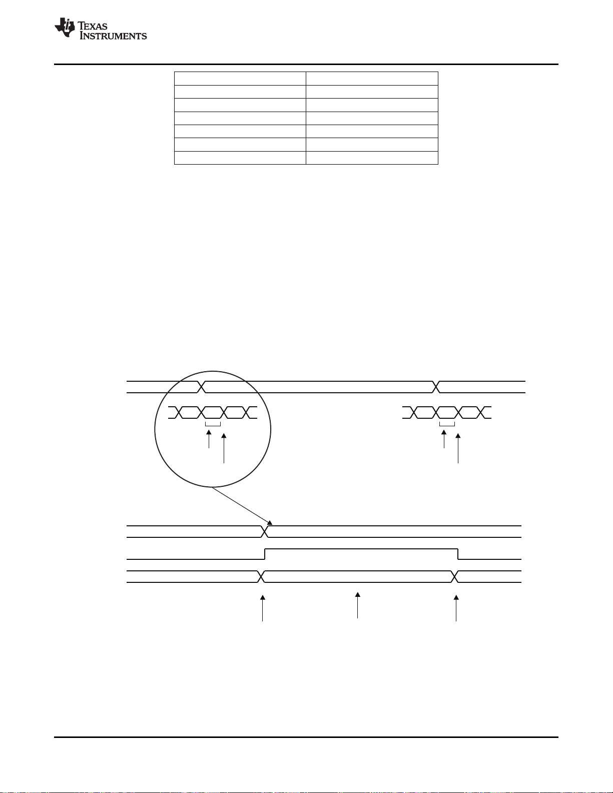
3
64
59 0
1
58
2Seconds
59 0
1
58
2
Hours
3 4Hours
59 0 1
Seconds
Compensation event
Compensation event
swcs046-015
TPS65910, TPS65910A, TPS65910A3, TPS659101, TPS659102, TPS659103
TPS659104, TPS659105, TPS659106, TPS659107, TPS659108, TPS659109
www.ti.com
Register Value
SECONDS_REG 0x36
MINUTES_REG 0x54
HOURS_REG 0x90
DAYS_REG 0x05
MONTHS_REG 0x09
YEARS_REG 0x08
The user can round to the closest minute, by setting the ROUND_30S register bit. TC values are set to the
closest minute value at the next second. The ROUND_30S bit is automatically cleared when the rounding time is
performed.
Example:
• If current time is 10H59M45S, a round operation changes time to 11H00M00S.
• if current time is 10H59M29S, a round operation changes time to 10H59M00S.
GENERAL REGISTERS
Software can access the RTC_STATUS_REG and RTC_CTRL_REG registers at any time (except for the
RTC_CTRL_REG[5] bit, which must be changed only when the RTC is stopped).
COMPENSATION REGISTERS
The RTC_COMP_MSB_REG and RTC_COMP_LSB_REG registers must respect the available access period.
These registers must be updated before each compensation process. For example, software can load the
compensation value into these registers after each hour event, during an available access period.
SWCS046T –MARCH 2010–REVISED SEPTEMBER 2013
Figure 17. RTC Compensation Scheduling
Copyright © 2010–2013, Texas Instruments Incorporated Submit Documentation Feedback 49
Product Folder Links: TPS65910 TPS65910A TPS65910A3 TPS659101 TPS659102 TPS659103 TPS659104
TPS659105 TPS659106 TPS659107 TPS659108 TPS659109

TPS65910, TPS65910A, TPS65910A3, TPS659101, TPS659102, TPS659103
TPS659104, TPS659105, TPS659106, TPS659107, TPS659108, TPS659109
SWCS046T –MARCH 2010–REVISED SEPTEMBER 2013
This drift can be balanced to compensate for any inaccuracy of the 32-kHz oscillator. Software must calibrate the
oscillator frequency, calculate the drift compensation versus one time hour period; and then load the
compensation registers with the drift compensation value. Indeed, if the AUTO_COMP_EN bit in the
RTC_CTRL_REG is enabled, the value of COMP_REG (in twos-complement) is added to the RTC 32-kHz
counter at each hour and one second. When COMP_REG is added to the RTC 32-kHz counter, the duration of
the current second becomes (32768 - COMP_REG)/32768s; so, the RTC can be compensated with a 1/32768
s/hour time unit accuracy.
NOTE
The compensation is considered once written into the registers.
BACKUP BATTERY MANAGEMENT
The device includes a back-up battery switch connecting the VRTC regulator input to a main battery (VCC7) or to
a back-up battery (VBACKUP), depending on the batteries voltage value.
The VRTC supply can then be maintained during a BACKUP state as far as the input voltage is high enough
(>VBNPR threshold). Below the VBNPR voltage threshold the digital core of the device is set under reset by
internal signal POR (PowerOnReset).
The back-up domain functions which are always supplied from VRTC comprehend:
• The internal 32-kHz oscillator
• Backup registers
The back-up battery can be charged from the main battery through an embedded charger. The back-up battery
charge voltage and enable is controlled through BBCH_REG register programming. This register content is
maintained during the device Backup state.
Hence enabled the back-up battery charge is maintained as far as the main battery voltage is higher than the
VMBLO threshold and the back-up battery voltage.
www.ti.com
BACKUP REGISTERS
As part of the RTC the device contains five 8-bit registers which can be used for storage by the application
firmware when the external host is powered down. These registers retain their content as long as the VRTC is
active.
I2C INTERFACE
A general-purpose serial control interface (CTL-I2C) allows read and write access to the configuration registers of
all resources of the system.
A second serial control interface (SR-I2C) is dedicated to SmartReflex applications such as DVFS or AVS.
Both control interfaces are compliant with HS-I2C specification.
These interfaces support the standard slave mode (100 Kbps), Fast mode (400 Kbps), and high-speed mode
(3.4 Mbps). The general-purpose I2C module using one slave hard-coded addresse (ID1 = 2Dh). The
SmartReflex I2C module uses one slave hard-coded address (ID0 = 12h). The master mode is not supported.
Addressing: Seven-bit mode addressing device
They do not support the following features:
• 10-bit addressing
• General call
THERMAL MONITORING AND SHUTDOWN
A thermal protection module monitors the junction temperature of the device versus two thesholds:
• Hot-die temperature threshold
• Thermal shutdown temperature theshold
50 Submit Documentation Feedback Copyright © 2010–2013, Texas Instruments Incorporated
Product Folder Links: TPS65910 TPS65910A TPS65910A3 TPS659101 TPS659102 TPS659103 TPS659104
TPS659105 TPS659106 TPS659107 TPS659108 TPS659109
TPS65910, TPS65910A, TPS65910A3, TPS659101, TPS659102, TPS659103
TPS659104, TPS659105, TPS659106, TPS659107, TPS659108, TPS659109
www.ti.com
When the hot-die temperature threshold is reached an interrupt is sent to software to close the noncritical running
tasks.
When the thermal shutdown temperature theshold is reached, the TPS65910 device is set under reset and a
transition to OFF state is initiated. Then the power-on enable conditions of the device is not considered until the
die temperature has decreased below the hot-die threshold. An hysteresis is applied to the hot-die and shutdown
threshold, when detecting a falling edge of temperature, and both detection are debounced to avoid any parasitic
detection. The TPS65910 device allows programming of four hot-die temperature thresholds to increase the
flexibility of the system.
By default, the thermal protection is enabled in ACTIVE state, but can be disabled through programming register
THERM_REG. The thermal protection can be enabled in SLEEP state programming register
SLEEP_KEEP_RES_ON. The thermal protection is automatically enabled during an OFF-to-ACTIVE state
transition and is kept enabled in OFF state after a switch-off sequence caused by a thermal shutdown event.
Transition to OFF state sequence caused by a thermal shutdown event is highlighted in the INT_STS_REG
status register. Recovery from this OFF state is initiated (switch-on sequence) when the die temperature falls
below the hot-die temperature threshold.
Hot-die and thermal shutdown temperature threshold detections state can be monitored or masked by reading or
programming the THERM_REG register. Hot-die interrupt can be masked by programming the INT_MSK_REG
register.
INTERRUPTS
SWCS046T –MARCH 2010–REVISED SEPTEMBER 2013
Table 13. Interrupt Sources
Interrupt Description
RTC_ALARM_IT RTC alarm event: Occurs at programmed determinate date and time
(running in ACTIVE, OFF, and SLEEP state, default inactive)
RTC_PERIOD_IT
HOT_DIE_IT
PWRHOLD_IT PWRHOLD signal rising edge
PWRON_LP_IT
PWRON_IT
VMBHI_IT
VMBDCH_IT
GPIO0_R_IT GPIO_CKSYNC rising-edge detection (available in ACTIVE and SLEEP state)
GPIO0_F_IT GPIO_CKSYNC falling-edge detection (available in ACTIVE and SLEEP state)
RTC periodic event: Occurs at programmed regular period of time (every second or minute)
(running in ACTIVE, OFF, and SLEEP state, default inactive)
The embedded thermal monitoring module has detected a die temperature above the hot-die
detection threshold (running in ACTIVE and SLEEP state)
Level sensitive interrupt.
PWRON is low during more than the long-press delay: t
register programming).
PWRON is low while the device is on (running in ACTIVE and SLEEP state) or PWON was
low while the device was off (causing a device turn-on). Level-sensitive interrupt
The battery voltage rise above the VMBHI threshold: NOSUPPLY to Off or Backup-to-Off
device states transition (first battery plug or battery voltage bounce detection). This interrupt
source can be disabled through EEPROM programming (VMBHI_IT_DIS). Edge-sensitive
interrupt
The battery voltage falls down below the VMBDCH threshold(running in ACTIVE and SLEEP
state, if enabled programming VMBCH_VSEL). Edge-sensitive interrupt
dPWRONLP
(can be disable though
INT1 signal (active low) warns the host processor of any event that occurred on the TPS65910 device. The host
processor can then poll the interrupt from the interrupt status register via I2C to identify the interrupt source. Each
interrupt source can be individually masked via the interrupt mask register.
Copyright © 2010–2013, Texas Instruments Incorporated Submit Documentation Feedback 51
Product Folder Links: TPS65910 TPS65910A TPS65910A3 TPS659101 TPS659102 TPS659103 TPS659104
TPS659105 TPS659106 TPS659107 TPS659108 TPS659109
TPS65910, TPS65910A, TPS65910A3, TPS659101, TPS659102, TPS659103
TPS659104, TPS659105, TPS659106, TPS659107, TPS659108, TPS659109
SWCS046T –MARCH 2010–REVISED SEPTEMBER 2013
PACKAGE DESCRIPTION
The following are the package descriptions of the TPS65910 PMU devices:
• Package type:
Package TPS65910
Type RSL QFN-N48
Size (mm) 6x6
Substrate layers 1 layer
Pitch ball array (mm) 0.4 mm
ViP (via-in-pad) No
Number of balls 48
Thickness (mm) (max. height including balls) 1
Others Green, ROHS-compliant
• Moisture sensitivity level target: JEDEC MSL3 @ 260°C
APPENDIX A: FUNCTIONAL REGISTERS
TPS65910_FUNC_REG REGISTERS MAPPING SUMMARY
Table 14. TPS65910_FUNC_REG Register Summary
Register Name Type Register Width (Bits) Register Reset Address Offset
SECONDS_REG RW 8 0x00 0x00
MINUTES_REG RW 8 0x00 0x01
HOURS_REG RW 8 0x00 0x02
DAYS_REG RW 8 0x01 0x03
MONTHS_REG RW 8 0x01 0x04
YEARS_REG RW 8 0x00 0x05
WEEKS_REG RW 8 0x00 0x06
ALARM_SECONDS_REG RW 8 0x00 0x08
ALARM_MINUTES_REG RW 8 0x00 0x09
ALARM_HOURS_REG RW 8 0x00 0x0A
ALARM_DAYS_REG RW 8 0x01 0x0B
ALARM_MONTHS_REG RW 8 0x01 0x0C
ALARM_YEARS_REG RW 8 0x00 0x0D
RTC_CTRL_REG RW 8 0x00 0x10
RTC_STATUS_REG RW 8 0x80 0x11
RTC_INTERRUPTS_REG RW 8 0x00 0x12
RTC_COMP_LSB_REG RW 8 0x00 0x13
RTC_COMP_MSB_REG RW 8 0x00 0x14
RTC_RES_PROG_REG RW 8 0x27 0x15
RTC_RESET_STATUS_REG RW 8 0x00 0x16
BCK1_REG RW 8 0x00 0x17
BCK2_REG RW 8 0x00 0x18
BCK3_REG RW 8 0x00 0x19
BCK4_REG RW 8 0x00 0x1A
BCK5_REG RW 8 0x00 0x1B
PUADEN_REG RW 8 0x9F 0x1C
REF_REG RW 8 0x01 0x1D
VRTC_REG RW 8 0x01 0x1E
VIO_REG RW 8 0x00 0x20
www.ti.com
52 Submit Documentation Feedback Copyright © 2010–2013, Texas Instruments Incorporated
Product Folder Links: TPS65910 TPS65910A TPS65910A3 TPS659101 TPS659102 TPS659103 TPS659104
TPS659105 TPS659106 TPS659107 TPS659108 TPS659109
TPS65910, TPS65910A, TPS65910A3, TPS659101, TPS659102, TPS659103
TPS659104, TPS659105, TPS659106, TPS659107, TPS659108, TPS659109
www.ti.com
Table 14. TPS65910_FUNC_REG Register Summary (continued)
Register Name Type Register Width (Bits) Register Reset Address Offset
VDD1_REG RW 8 0x0C 0x21
VDD1_OP_REG RW 8 0x00 0x22
VDD1_SR_REG RW 8 0x00 0x23
VDD2_REG RW 8 0x04 0x24
VDD2_OP_REG RW 8 0x00 0x25
VDD2_SR_REG RW 8 0x00 0x26
VDD3_REG RW 8 0x04 0x27
VDIG1_REG RW 8 0x00 0x30
VDIG2_REG RW 8 0x00 0x31
VAUX1_REG RW 8 0x00 0x32
VAUX2_REG RW 8 0x00 0x33
VAUX33_REG RW 8 0x00 0x34
VMMC_REG RW 8 0x00 0x35
VPLL_REG RW 8 0x00 0x36
VDAC_REG RW 8 0x00 0x37
THERM_REG RW 8 0x0D 0x38
BBCH_REG RW 8 0x00 0x39
DCDCCTRL_REG RW 8 0x3B 0x3E
DEVCTRL_REG RW 8 0x40 0x3F
DEVCTRL2_REG RW 8 0x34 0x40
SLEEP_KEEP_LDO_ON_REG RW 8 0x00 0x41
SLEEP_KEEP_RES_ON_REG RW 8 0x00 0x42
SLEEP_SET_LDO_OFF_REG RW 8 0x00 0x43
SLEEP_SET_RES_OFF_REG RW 8 0x00 0x44
EN1_LDO_ASS_REG RW 8 0x00 0x45
EN1_SMPS_ASS_REG RW 8 0x00 0x46
EN2_LDO_ASS_REG RW 8 0x00 0x47
EN2_SMPS_ASS_REG RW 8 0x00 0x48
RESERVED RW 8 0x00 0x49
RESERVED RW 8 0x00 0x4A
INT_STS_REG RW 8 0x00 0x50
INT_MSK_REG RW 8 0x02 0x51
INT_STS2_REG RW 8 0x00 0x52
INT_MSK2_REG RW 8 0x00 0x53
GPIO0_REG RW 8 0x0A 0x60
JTAGVERNUM_REG RO 8 0x00 0x80
SWCS046T –MARCH 2010–REVISED SEPTEMBER 2013
TPS65910_FUNC_REG REGISTER DESCRIPTIONS
Table 15. SECONDS_REG
Address Offset 0x00
Physical Address Instance
Description RTC register for seconds
Type RW
Copyright © 2010–2013, Texas Instruments Incorporated Submit Documentation Feedback 53
Product Folder Links: TPS65910 TPS65910A TPS65910A3 TPS659101 TPS659102 TPS659103 TPS659104
TPS659105 TPS659106 TPS659107 TPS659108 TPS659109
TPS65910, TPS65910A, TPS65910A3, TPS659101, TPS659102, TPS659103
TPS659104, TPS659105, TPS659106, TPS659107, TPS659108, TPS659109
SWCS046T –MARCH 2010–REVISED SEPTEMBER 2013
7 6 5 4 3 2 1 0
Reserved SEC1 SEC0
Bits Field Name Description Type Reset
7 Reserved Reserved bit RO 0
R returns
0s
6:4 SEC1 Second digit of seconds (range is 0 up to 5) RW 0x0
3:0 SEC0 First digit of seconds (range is 0 up to 9) RW 0x0
Table 16. MINUTES_REG
Address Offset 0x01
Physical Address Instance
Description RTC register for minutes
Type RW
7 6 5 4 3 2 1 0
Reserved MIN1 MIN0
Bits Field Name Description Type Reset
7 Reserved Reserved bit RO 0
R returns
0s
6:4 MIN1 Second digit of minutes (range is 0 up to 5) RW 0x0
3:0 MIN0 First digit of minutes (range is 0 up to 9) RW 0x0
www.ti.com
Table 17. HOURS_REG
Address Offset 0x02
Physical Address Instance
Description RTC register for hours
Type RW
7 6 5 4 3 2 1 0
PM_NAM Reserved HOUR1 HOUR0
Bits Field Name Description Type Reset
7 PM_NAM Only used in PM_AM mode (otherwise it is set to 0) RW 0
6 Reserved Reserved bit RO 0
5:4 HOUR1 Second digit of hours(range is 0 up to 2) RW 0x0
3:0 HOUR0 First digit of hours (range is 0 up to 9) RW 0x0
0 is AM
1 is PM
R returns
0s
Table 18. DAYS_REG
Address Offset 0x03
Physical Address Instance
Description RTC register for days
Type RW
54 Submit Documentation Feedback Copyright © 2010–2013, Texas Instruments Incorporated
Product Folder Links: TPS65910 TPS65910A TPS65910A3 TPS659101 TPS659102 TPS659103 TPS659104
TPS659105 TPS659106 TPS659107 TPS659108 TPS659109

TPS65910, TPS65910A, TPS65910A3, TPS659101, TPS659102, TPS659103
TPS659104, TPS659105, TPS659106, TPS659107, TPS659108, TPS659109
www.ti.com
7 6 5 4 3 2 1 0
Reserved DAY1 DAY0
Bits Field Name Description Type Reset
7:6 Reserved Reserved bit RO 0x0
5:4 DAY1 Second digit of days (range is 0 up to 3) RW 0x0
3:0 DAY0 First digit of days (range is 0 up to 9) RW 0x1
Table 19. MONTHS_REG
Address Offset 0x04
Physical Address Instance
Description RTC register for months
Type RW
7 6 5 4 3 2 1 0
Reserved MONTH1 MONTH0
Bits Field Name Description Type Reset
7:5 Reserved Reserved bit RO 0x0
4 MONTH1 Second digit of months (range is 0 up to 1) RW 0
3:0 MONTH0 First digit of months (range is 0 up to 9) RW 0x1
SWCS046T –MARCH 2010–REVISED SEPTEMBER 2013
R returns
0s
R returns
0s
Table 20. YEARS_REG
Address Offset 0x05
Physical Address Instance
Description RTC register for day of the week
Type RW
7 6 5 4 3 2 1 0
YEAR1 YEAR0
Bits Field Name Description Type Reset
7:4 YEAR1 Second digit of years (range is 0 up to 9) RW 0x0
3:0 YEAR0 First digit of years (range is 0 up to 9) RW 0x0
Table 21. WEEKS_REG
Address Offset 0x06
Physical Address Instance
Description RTC register for day of the week
Type RW
7 6 5 4 3 2 1 0
Reserved WEEK
Copyright © 2010–2013, Texas Instruments Incorporated Submit Documentation Feedback 55
Product Folder Links: TPS65910 TPS65910A TPS65910A3 TPS659101 TPS659102 TPS659103 TPS659104
TPS659105 TPS659106 TPS659107 TPS659108 TPS659109
TPS65910, TPS65910A, TPS65910A3, TPS659101, TPS659102, TPS659103
TPS659104, TPS659105, TPS659106, TPS659107, TPS659108, TPS659109
SWCS046T –MARCH 2010–REVISED SEPTEMBER 2013
Bits Field Name Description Type Reset
7:3 Reserved Reserved bit RO 0x00
R returns
0s
2:0 WEEK First digit of day of the week (range is 0 up to 6) RW 0
Table 22. ALARM_SECONDS_REG
Address Offset 0x08
Physical Address Instance
Description RTC register for alarm programmation for seconds
Type RW
7 6 5 4 3 2 1 0
Reserved ALARM_SEC1 ALARM_SEC0
Bits Field Name Description Type Reset
7 Reserved Reserved bit RO 0
R returns
0s
6:4 ALARM_SEC1 Second digit of alarm programmation for seconds (range is 0 up to 5) RW 0x0
3:0 ALARM_SEC0 First digit of alarm programmation for seconds (range is 0 up to 9) RW 0x0
www.ti.com
Table 23. ALARM_MINUTES_REG
Address Offset 0x09
Physical Address Instance
Description RTC register for alarm programmation for minutes
Type RW
7 6 5 4 3 2 1 0
Reserved ALARM_MIN1 ALARM_MIN0
Bits Field Name Description Type Reset
7 Reserved Reserved bit RO 0
6:4 ALARM_MIN1 Second digit of alarm programmation for minutes (range is 0 up to 5) RW 0x0
3:0 ALARM_MIN0 First digit of alarm programmation for minutes (range is 0 up to 9) RW 0x0
R returns
0s
Table 24. ALARM_HOURS_REG
Address Offset 0x0A
Physical Address Instance
Description RTC register for alarm programmation for hours
Type RW
7 6 5 4 3 2 1 0
Reserved ALARM_HOUR1 ALARM_HOUR0
ALARM_PM_NAM
56 Submit Documentation Feedback Copyright © 2010–2013, Texas Instruments Incorporated
Product Folder Links: TPS65910 TPS65910A TPS65910A3 TPS659101 TPS659102 TPS659103 TPS659104
TPS659105 TPS659106 TPS659107 TPS659108 TPS659109
TPS65910, TPS65910A, TPS65910A3, TPS659101, TPS659102, TPS659103
TPS659104, TPS659105, TPS659106, TPS659107, TPS659108, TPS659109
www.ti.com
Bits Field Name Description Type Reset
7 ALARM_PM_NAM Only used in PM_AM mode for alarm programmation (otherwise it is set RW 0
to 0)
0 is AM
1 is PM
6 Reserved Reserved bit RO 0
5:4 ALARM_HOUR1 Second digit of alarm programmation for hours(range is 0 up to 2) RW 0x0
3:0 ALARM_HOUR0 First digitof alarm programmation for hours (range is 0 up to 9) RW 0x0
Table 25. ALARM_DAYS_REG
Address Offset 0x0B
Physical Address Instance
Description RTC register for alarm programmation for days
Type RW
7 6 5 4 3 2 1 0
Reserved ALARM_DAY1 ALARM_DAY0
Bits Field Name Description Type Reset
7:6 Reserved Reserved bit RO 0x0
5:4 ALARM_DAY1 Second digit of alarm programmation for days (range is 0 up to 3) RW 0x0
3:0 ALARM_DAY0 First digit of alarm programmation for days (range is 0 up to 9) RW 0x1
SWCS046T –MARCH 2010–REVISED SEPTEMBER 2013
R returns
0s
R Special
Table 26. ALARM_MONTHS_REG
Address Offset 0x0C
Physical Address Instance
Description RTC register for alarm programmation for months
Type RW
7 6 5 4 3 2 1 0
Reserved ALARM_MONTH0
ALARM_MONTH1
Bits Field Name Description Type Reset
7:5 Reserved Reserved bit RO 0x0
4 ALARM_MONTH1 Second digit of alarm programmation for months (range is 0 up to 1) RW 0
3:0 ALARM_MONTH0 First digit of alarm programmation for months (range is 0 up to 9) RW 0x1
R returns
0s
Table 27. ALARM_YEARS_REG
Address Offset 0x0D
Physical Address Instance
Description RTC register for alarm programmation for years
Type RW
Copyright © 2010–2013, Texas Instruments Incorporated Submit Documentation Feedback 57
Product Folder Links: TPS65910 TPS65910A TPS65910A3 TPS659101 TPS659102 TPS659103 TPS659104
TPS659105 TPS659106 TPS659107 TPS659108 TPS659109

TPS65910, TPS65910A, TPS65910A3, TPS659101, TPS659102, TPS659103
TPS659104, TPS659105, TPS659106, TPS659107, TPS659108, TPS659109
SWCS046T –MARCH 2010–REVISED SEPTEMBER 2013
7 6 5 4 3 2 1 0
ALARM_YEAR1 ALARM_YEAR0
Bits Field Name Description Type Reset
7:4 ALARM_YEAR1 Second digit of alarm programmation for years (range is 0 up to 9) RW 0x0
3:0 ALARM_YEAR0 First digit of alarm programmation for years (range is 0 up to 9) RW 0x0
Table 28. RTC_CTRL_REG
Address Offset 0x10
Physical Address Instance
Description RTC control register:
NOTES: A dummy read of this register is necessary before each I2C read in order to update the
ROUND_30S bit value.
Type RW
7 6 5 4 3 2 1 0
RTC_V_OPT GET_TIME TEST_MODE MODE_12_24 AUTO_COMP ROUND_30S STOP_RTC
www.ti.com
SET_32_COUNTER
Bits Field Name Description Type Reset
7 RTC_V_OPT RTC date / time register selection: RW 0
6 GET_TIME When writing a 1 into this register, the content of the dynamic registers RW 0
5 SET_32_COUNTER 0: No action RW 0
4 TEST_MODE 0: functional mode RW 0
3 MODE_12_24 0: 24 hours mode RW 0
2 AUTO_COMP 0: No auto compensation RW 0
1 ROUND_30S 0: No update RW 0
0 STOP_RTC 0: RTC is frozen RW 0
0: Read access directly to dynamic registers (SECONDS_REG,
MINUTES_REG, HOURS_REG, DAYS_REG, MONTHS_REG,
YEAR_REG, WEEKS_REG)
1: Read access to static shadowed registers: (see GET_TIME bit).
(SECONDS_REG, MINUTES_REG, HOURS_REG, DAYS_REG,
MONTHS_REG, YEAR_REG and WEEKS_REG) is transferred into
static shadowed registers. Each update of the shadowed registers needs
to be done by re-asserting GET_TIME bit to 1 (i.e.: reset it to 0 and then
re-write it to 1)
1: set the 32-kHz counter with COMP_REG value.
It must only be used when the RTC is frozen.
1: test mode (Auto compensation is enable when the 32kHz counter
reaches at its end)
1: 12 hours mode (PM-AM mode)
It is possible to switch between the two modes at any time without
disturbed the RTC, read or write are always performed with the current
mode.
1: Auto compensation enabled
1: When a one is written, the time is rounded to the closest minute.
This bit is a toggle bit, the micro-controller can only write one and RTC
clears it. If the micro-controller sets the ROUND_30S bit and then read it,
the micro-controller will read one until the rounded to the closet.
1: RTC is running
58 Submit Documentation Feedback Copyright © 2010–2013, Texas Instruments Incorporated
Product Folder Links: TPS65910 TPS65910A TPS65910A3 TPS659101 TPS659102 TPS659103 TPS659104
TPS659105 TPS659106 TPS659107 TPS659108 TPS659109

TPS65910, TPS65910A, TPS65910A3, TPS659101, TPS659102, TPS659103
TPS659104, TPS659105, TPS659106, TPS659107, TPS659108, TPS659109
www.ti.com
Table 29. RTC_STATUS_REG
Address Offset 0x11
Physical Address Instance
Description RTC status register:
NOTES: A dummy read of this register is necessary before each I2C read in order to update the status
register value.
Type RW
7 6 5 4 3 2 1 0
POWER_UP ALARM EVENT_1D EVENT_1H EVENT_1M EVENT_1S RUN Reserved
Bits Field Name Description Type Reset
7 POWER_UP Indicates that a reset occurred (bit cleared to 0 by writing 1). RW 1
POWER_UP is set by a reset, is cleared by writing one in this bit.
6 ALARM Indicates that an alarm interrupt has been generated (bit clear by writing RW 0
1).
The alarm interrupt keeps its low level, until the micro-controller write 1 in
the ALARM bit of the RTC_STATUS_REG register.
The timer interrupt is a low-level pulse (15 µs duration).
5 EVENT_1D One day has occurred RO 0
4 EVENT_1H One hour has occurred RO 0
3 EVENT_1M One minute has occurred RO 0
2 EVENT_1S One second has occurred RO 0
1 RUN 0: RTC is frozen RO 0
1: RTC is running
This bit shows the real state of the RTC, indeed because of STOP_RTC
signal was resynchronized on 32-kHz clock, the action of this bit is
delayed.
0 Reserved Reserved bit RO 0
SWCS046T –MARCH 2010–REVISED SEPTEMBER 2013
R returns
0s
Table 30. RTC_INTERRUPTS_REG
Address Offset 0x12
Physical Address Instance
Description RTC interrupt control register
Type RW
7 6 5 4 3 2 1 0
Reserved IT_ALARM IT_TIMER EVERY
IT_SLEEP_MASK_EN
Bits Field Name Description Type Reset
7:5 Reserved Reserved bit RO 0x0
4 IT_SLEEP_MASK_E 1: Mask periodic interrupt while the TPS65910 device is in SLEEP mode. RW 0
N Interrupt event is back up in a register and occurred as soon as the
TPS65910 device is no more in SLEEP mode.
0: Normal mode, no interrupt masked
R returns
0s
Copyright © 2010–2013, Texas Instruments Incorporated Submit Documentation Feedback 59
Product Folder Links: TPS65910 TPS65910A TPS65910A3 TPS659101 TPS659102 TPS659103 TPS659104
TPS659105 TPS659106 TPS659107 TPS659108 TPS659109

TPS65910, TPS65910A, TPS65910A3, TPS659101, TPS659102, TPS659103
TPS659104, TPS659105, TPS659106, TPS659107, TPS659108, TPS659109
SWCS046T –MARCH 2010–REVISED SEPTEMBER 2013
Bits Field Name Description Type Reset
3 IT_ALARM Enable one interrupt when the alarm value is reached (TC ALARM RW 0
registers) by the TC registers
2 IT_TIMER Enable periodic interrupt RW 0
0: interrupt disabled
1: interrupt enabled
1:0 EVERY Interrupt period RW 0x0
00: every second
01: every minute
10: every hour
11: every day
Table 31. RTC_COMP_LSB_REG
Address Offset 0x13
Physical Address Instance
Description RTC compensation register (LSB)
Notes: This register must be written in 2-complement.
This means that to add one 32kHz oscillator period every hour, micro-controller needs to write FFFF into
RTC_COMP_MSB_REG & RTC_COMP_LSB_REG.
To remove one 32-kHz oscillator period every hour, micro-controller needs to write 0001 into
RTC_COMP_MSB_REG & RTC_COMP_LSB_REG.
The 7FFF value is forbidden.
Type RW
www.ti.com
7 6 5 4 3 2 1 0
RTC_COMP_LSB
Bits Field Name Description Type Reset
7:0 RTC_COMP_LSB This register contains the number of 32-kHz periods to be added into the RW 0x00
32-kHz counter every hour [LSB]
Table 32. RTC_COMP_MSB_REG
Address Offset 0x14
Physical Address Instance
Description RTC compensation register (MSB)
Type RW
7 6 5 4 3 2 1 0
Bits Field Name Description Type Reset
7:0 RTC_COMP_MSB This register contains the number of 32-kHz periods to be added into the RW 0x00
Notes: See RTC_COMP_LSB_REG Notes.
RTC_COMP_MSB
32-kHz counter every hour [MSB]
Table 33. RTC_RES_PROG_REG
Address Offset 0x15
Physical Address Instance
Description RTC register containing oscillator resistance value
Type RW
7 6 5 4 3 2 1 0
Reserved SW_RES_PROG
60 Submit Documentation Feedback Copyright © 2010–2013, Texas Instruments Incorporated
Product Folder Links: TPS65910 TPS65910A TPS65910A3 TPS659101 TPS659102 TPS659103 TPS659104
TPS659105 TPS659106 TPS659107 TPS659108 TPS659109

TPS65910, TPS65910A, TPS65910A3, TPS659101, TPS659102, TPS659103
TPS659104, TPS659105, TPS659106, TPS659107, TPS659108, TPS659109
www.ti.com
Bits Field Name Description Type Reset
7:6 Reserved Reserved bit RO 0x0
5:0 SW_RES_PROG Value of the oscillator resistance RW 0x27
Table 34. RTC_RESET_STATUS_REG
Address Offset 0x16
Physical Address Instance
Description RTC register for reset status
Type RW
7 6 5 4 3 2 1 0
Reserved
SWCS046T –MARCH 2010–REVISED SEPTEMBER 2013
R returns
0s
RESET_STATUS
Bits Field Name Description Type Reset
7:1 Reserved Reserved bit RO 0x0
0 RESET_STATUS RW 0x0
R returns
0s
Table 35. BCK1_REG
Address Offset 0x17
Physical Address Instance
Description Backup register which can be used for storage by the application firmware when the external host is
Type RW
7 6 5 4 3 2 1 0
Bits Field Name Description Type Reset
7:0 BCKUP Backup bit RW 0x00
powered down. These registers will retain their content as long as the VRTC is active.
BCKUP
Table 36. BCK2_REG
Address Offset 0x18
Physical Address Instance
Description Backup register which can be used for storage by the application firmware when the external host is
Type RW
powered down. These registers will retain their content as long as the VRTC is active.
7 6 5 4 3 2 1 0
BCKUP
Bits Field Name Description Type Reset
7:0 BCKUP Backup bit RW 0x00
Copyright © 2010–2013, Texas Instruments Incorporated Submit Documentation Feedback 61
Product Folder Links: TPS65910 TPS65910A TPS65910A3 TPS659101 TPS659102 TPS659103 TPS659104
TPS659105 TPS659106 TPS659107 TPS659108 TPS659109

TPS65910, TPS65910A, TPS65910A3, TPS659101, TPS659102, TPS659103
TPS659104, TPS659105, TPS659106, TPS659107, TPS659108, TPS659109
SWCS046T –MARCH 2010–REVISED SEPTEMBER 2013
Table 37. BCK3_REG
Address Offset 0x19
Physical Address Instance
Description Backup register which can be used for storage by the application firmware when the external host is
powered down. These registers will retain their content as long as the VRTC is active.
Type RW
7 6 5 4 3 2 1 0
BCKUP
Bits Field Name Description Type Reset
7:0 BCKUP Backup bit RW 0x00
Table 38. BCK4_REG
Address Offset 0x1A
Physical Address Instance
Description Backup register which can be used for storage by the application firmware when the external host is
powered down. These registers will retain their content as long as the VRTC is active.
Type RW
www.ti.com
7 6 5 4 3 2 1 0
BCKUP
Bits Field Name Description Type Reset
7:0 BCKUP Backup bit RW 0x00
Table 39. BCK5_REG
Address Offset 0x1B
Physical Address Instance
Description Backup register which can be used for storage by the application firmware when the external host is
Type RW
7 6 5 4 3 2 1 0
Bits Field Name Description Type Reset
7:0 BCKUP Backup bit RW 0x00
powered down. These registers will retain their content as long as the VRTC is active.
BCKUP
Table 40. PUADEN_REG
Address Offset 0x1C
Physical Address Instance
Description Pull-up/pull-down control register.
Type RW
7 6 5 4 3 2 1 0
RESERVED I2CCTLP I2CSRP PWRONP SLEEPP PWRHOLDP BOOT1P BOOT0P
62 Submit Documentation Feedback Copyright © 2010–2013, Texas Instruments Incorporated
Product Folder Links: TPS65910 TPS65910A TPS65910A3 TPS659101 TPS659102 TPS659103 TPS659104
TPS659105 TPS659106 TPS659107 TPS659108 TPS659109

TPS65910, TPS65910A, TPS65910A3, TPS659101, TPS659102, TPS659103
TPS659104, TPS659105, TPS659106, TPS659107, TPS659108, TPS659109
www.ti.com
Bits Field Name Description Type Reset
7 RESERVED Reserved bit RW 1
6 I2CCTLP SDACTL and SCLCTL pull-up control: RW 0
1: Pull-up is enabled
0: Pull-up is disabled
5 I2CSRP SDASR and SCLSR pull-up control: RW 0
1: Pull-up is enabled
0: Pull-up is disabled
4 PWRONP PWRON pad pull-up control: RW 1
1: Pull-up is enabled
0: Pull-up is disabled
3 SLEEPP SLEEP pad pull-down control: RW 1
1: Pull-down is enabled
0: Pull-down is disabled
2 PWRHOLDP PWRHOLD pad pull-down control: RW 1
1: Pull-down is enabled
0: Pull-down is disabled
1 BOOT1P BOOT1 pad control: RW 1
1: Pull-down is enabled
0: Pull-down is disabled
0 BOOT0P BOOT0 pad control: RW 1
1: Pull-down is enabled
0: Pull-down is disabled
SWCS046T –MARCH 2010–REVISED SEPTEMBER 2013
Table 41. REF_REG
Address Offset 0x1D
Physical Address Instance
Description Reference control register
Type RW
7 6 5 4 3 2 1 0
Reserved VMBCH_SEL ST
Bits Field Name Description Type Reset
7:4 Reserved Reserved bit RO 0x0
3:2 VMBCH_SEL Main Battery comparator VMBCH programmable threshold (EEPROM RW 0x0
bits):
VMBCH_SEL[1:0] = 00 : bypass
VMBCH_SEL[1:0] = 01 : VMBCH = 2.8 V
VMBCH_SEL[1:0] = 10 : VMBCH = 2.9 V
VMBCH_SEL[1:0] = 11 : VMBCH = 3.0 V
1:0 ST Reference state: RO 0x1
ST[1:0] = 00 : Off
ST[1:0] = 01 : On high power (ACTIVE)
ST[1:0] = 10 : Reserved
ST[1:0] = 11 : On low power (SLEEP)
(Write access available in test mode only)
R returns
0s
Table 42. VRTC_REG
Address Offset 0x1E
Physical Address Instance
Description VRTC internal regulator control register
Type RW
Copyright © 2010–2013, Texas Instruments Incorporated Submit Documentation Feedback 63
Product Folder Links: TPS65910 TPS65910A TPS65910A3 TPS659101 TPS659102 TPS659103 TPS659104
TPS659105 TPS659106 TPS659107 TPS659108 TPS659109

TPS65910, TPS65910A, TPS65910A3, TPS659101, TPS659102, TPS659103
TPS659104, TPS659105, TPS659106, TPS659107, TPS659108, TPS659109
SWCS046T –MARCH 2010–REVISED SEPTEMBER 2013
7 6 5 4 3 2 1 0
Reserved Reserved ST
VRTC_OFFMASK
Bits Field Name Description Type Reset
7:4 Reserved Reserved bit RO 0x0
R returns
0s
3 VRTC_OFFMASK VRTC internal regulator off mask signal: RW 0
when 1, the regulator keeps its full-load capability during device OFF
state.
when 0, the regulator will enter in low-power mode during device OFF
state.(EEPROM bit)
2 Reserved Reserved bit RO 0
R returns
0s
1:0 ST Reference state: RO 0x1
ST[1:0] = 00 : Reserved
ST[1:0] = 01 : On high power (ACTIVE)
ST[1:0] = 10 : Reserved
ST[1:0] = 11 : On low power (SLEEP)
(Write access available in test mode only)
www.ti.com
Table 43. VIO_REG
Address Offset 0x20
Physical Address Instance
Description VIO control register
Type RW
7 6 5 4 3 2 1 0
ILMAX Reserved SEL ST
Bits Field Name Description Type Reset
7:6 ILMAX Select maximum load current: RW 0x0
5:4 Reserved Reserved bit RO 0x0
3:2 SEL Output voltage selection (EEPROM bits): RW See
1:0 ST Supply state (EEPROM bits): RW 0x0
(1) The reset value for this field varies with boot mode selection and the processor support. Please refer to the corresponding processor
user guide to find the correct default value.
when 00: 0.5 A
when 01: 1.0 A
when 10: 1.0 A
when 11: 1.0 A
R returns
0s
(1)
SEL[1:0] = 00 : 1.5 V
SEL[1:0] = 01 : 1.8 V
SEL[1:0] = 10 : 2.5 V
SEL[1:0] = 11 : 3.3 V
ST[1:0] = 00 : Off
ST[1:0] = 01 : On high power (ACTIVE)
ST[1:0] = 10 : Off
ST[1:0] = 11 : On low power (SLEEP)
(Write access available in test mode only)
64 Submit Documentation Feedback Copyright © 2010–2013, Texas Instruments Incorporated
Product Folder Links: TPS65910 TPS65910A TPS65910A3 TPS659101 TPS659102 TPS659103 TPS659104
TPS659105 TPS659106 TPS659107 TPS659108 TPS659109

TPS65910, TPS65910A, TPS65910A3, TPS659101, TPS659102, TPS659103
TPS659104, TPS659105, TPS659106, TPS659107, TPS659108, TPS659109
www.ti.com
Table 44. VDD1_REG
Address Offset 0x21
Physical Address Instance
Description VDD1 control register
Type RW
7 6 5 4 3 2 1 0
VGAIN_SEL ILMAX TSTEP ST
Bits Field Name Description Type Reset
7:6 VGAIN_SEL Select output voltage multiplication factor: G (EEPROM bits): RW 0x0
when 00: x1
when 01: x1
when 10: x2
when 11: x3
5:4 ILMAX Select maximum load current: RW 0
when 0: 1.0 A
when 1: 1.5 A
3:2 TSTEP Time step: when changing the output voltage, the new value is reached RW 0x3
through successive 12.5 mV voltage steps (if not bypassed). The
equivalent programmable slew rate of the output voltage is then:
TSTEP[2:0] = 000 : step duration is 0, step function is bypassed
TSTEP[2:0] = 001 : 12.5 mV/µs (sampling 3 Mhz)
TSTEP[2:0] = 010 : 9.4 mV/µs (sampling 3 Mhz × 3/4)
TSTEP[2:0] = 011 : 7.5 mV/µs (sampling 3 Mhz × 3/5) (default)
TSTEP[2:0] = 100 : 6.25 mV/µs(sampling 3 Mhz/2)
TSTEP[2:0] = 101 : 4.7 mV/µs(sampling 3 Mhz/3)
TSTEP[2:0] = 110 : 3.12 mV/µs(sampling 3 Mhz/4)
TSTEP[2:0] = 111 : 2.5 mV/µs(sampling 3 Mhz/5)
1:0 ST Supply state (EEPROM bits): RW 0x0
ST[1:0] = 00 : Off
ST[1:0] = 01 : On, high power mode
ST[1:0] = 10 : Off
ST[1:0] = 11 : On, low power mode
SWCS046T –MARCH 2010–REVISED SEPTEMBER 2013
Table 45. VDD1_OP_REG
Address Offset 0x22
Physical Address Instance
Description VDD1 voltage selection register.
Type RW
7 6 5 4 3 2 1 0
CMD SEL
Copyright © 2010–2013, Texas Instruments Incorporated Submit Documentation Feedback 65
Product Folder Links: TPS65910 TPS65910A TPS65910A3 TPS659101 TPS659102 TPS659103 TPS659104
This register can be accessed by both control and smartreflex I2C interfaces depending on
SR_CTL_I2C_SEL register bit value.
TPS659105 TPS659106 TPS659107 TPS659108 TPS659109

TPS65910, TPS65910A, TPS65910A3, TPS659101, TPS659102, TPS659103
TPS659104, TPS659105, TPS659106, TPS659107, TPS659108, TPS659109
SWCS046T –MARCH 2010–REVISED SEPTEMBER 2013
Bits Field Name Description Type Reset
7 CMD Smart-Reflex command: RW 0
when 0: VDD1_OP_REG voltage is applied
when 1: VDD1_SR_REG voltage is applied
6:0 SEL Output voltage (EEPROM bits) selection with GAIN_SEL = 00 (G = 1, RW See
12.5 mV per LSB):
SEL[6:0] = 1001011 to 1111111 : 1.5 V
...
SEL[6:0] = 0111111 : 1.35 V
...
SEL[6:0] = 0110011 : 1.2 V
...
SEL[6:0] = 0000001 to 0000011 : 0.6 V
SEL[6:0] = 0000000 : Off (0.0 V)
Note: from SEL[6:0] = 3 to 75 (dec)
Vout = (SEL[6:0] × 12.5 mV + 0.5625 V) × G
(1) The reset value for this field varies with boot mode selection and the processor support. Please refer to the corresponding processor
user guide to find the correct default value.
Table 46. VDD1_SR_REG
Address Offset 0x23
Physical Address Instance
Description VDD1 voltage selection register for smartreflex.
This register can be accessed by both control and smartreflex I2C interfaces depending on
SR_CTL_I2C_SEL register bit value.
Type RW
www.ti.com
(1)
7 6 5 4 3 2 1 0
Reserved SEL
Bits Field Name Description Type Reset
7 Reserved Reserved bit RO 0
6:0 SEL Output voltage (EEPROM bits) selection with GAIN_SEL = 00 (G = 1, RW See
12.5 mV per LSB):
SEL[6:0] = 1001011 to 1111111 : 1.5V
...
SEL[6:0] = 0111111 : 1.35V
...
SEL[6:0] = 0110011 : 1.2V
...
SEL[6:0] = 0000001 to 0000011 : 0.6V
SEL[6:0] = 0000000 : Off (0.0V)
Note: from SEL[6:0] = 3 to 75 (dec)
Vout = (SEL[6:0] × 12.5 mV + 0.5625 V) × G
(1) The reset value for this field varies with boot mode selection and the processor support. Please refer to the corresponding processor
user guide to find the correct default value.
R returns
0s
(1)
Table 47. VDD2_REG
Address Offset 0x24
Physical Address Instance
Description VDD2 control register
Type RW
7 6 5 4 3 2 1 0
VGAIN_SEL ILMAX TSTEP ST
66 Submit Documentation Feedback Copyright © 2010–2013, Texas Instruments Incorporated
Product Folder Links: TPS65910 TPS65910A TPS65910A3 TPS659101 TPS659102 TPS659103 TPS659104
TPS659105 TPS659106 TPS659107 TPS659108 TPS659109

TPS65910, TPS65910A, TPS65910A3, TPS659101, TPS659102, TPS659103
TPS659104, TPS659105, TPS659106, TPS659107, TPS659108, TPS659109
www.ti.com
Bits Field Name Description Type Reset
7:6 VGAIN_SEL Select output voltage multiplication factor: G (EEPROM bits): RW 0x0
when 00: x1
when 01: x1
when 10: x2
when 11: x3
5:4 ILMAX Select maximum load current: RW 0
when 0: 1.0 A
when 1: 1.5 A
3:2 TSTEP Time step: when changing the output voltage, the new value is reached RW 0x1
through successive 12.5 mV voltage steps (if not bypassed). The
equivalent programmable slew rate of the output voltage is then:
TSTEP[2:0] = 000: step duration is 0, step function is bypassed
TSTEP[2:0] = 001: 12.5 mV/µs (sampling 3 Mhz)
TSTEP[2:0] = 010: 9.4 mV/µs (sampling 3 Mhz × 3/4)
TSTEP[2:0] = 011: 7.5 mV/µs (sampling 3 Mhz × 3/5) (default)
TSTEP[2:0] = 100: 6.25 mV/µs(sampling 3 Mhz/2)
TSTEP[2:0] = 101: 4.7 mV/µs(sampling 3 Mhz/3)
TSTEP[2:0] = 110: 3.12 mV/µs(sampling 3 Mhz/4)
TSTEP[2:0] = 111: 2.5 mV/µs(sampling 3 Mhz/5)
1:0 ST Supply state (EEPROM bits): RW 0x0
ST[1:0] = 00 : Off
ST[1:0] = 01 : On, high power mode
ST[1:0] = 10 : Off
ST[1:0] = 11 : On, low power mode
SWCS046T –MARCH 2010–REVISED SEPTEMBER 2013
Table 48. VDD2_OP_REG
Address Offset 0x25
Physical Address Instance
Description VDD2 voltage selection register.
Type RW
7 6 5 4 3 2 1 0
CMD SEL
Bits Field Name Description Type Reset
7 CMD Smart-Reflex command: RW 0
6:0 SEL Output voltage (EEPROM bits) selection with GAIN_SEL = 00 (G = 1, RW See
(1) The reset value for this field varies with boot mode selection and the processor support. Please refer to the corresponding processor
user guide to find the correct default value.
This register can be accessed by both control and smartreflex I2C interfaces depending on
SR_CTL_I2C_SEL register bit value.
when 0: VDD2_OP_REG voltage is applied
when 1: VDD2_SR_REG voltage is applied
(1)
12.5 mV per LSB):
SEL[6:0] = 1001011 to 1111111 : 1.5 V
...
SEL[6:0] = 0111111 : 1.35 V
...
SEL[6:0] = 0110011 : 1.2 V
...
SEL[6:0] = 0000001 to 0000011 : 0.6 V
SEL[6:0] = 0000000 : Off (0.0 V)
Note: from SEL[6:0] = 3 to 75 (dec)
Vout= (SEL[6:0] × 12.5 mV + 0.5625 V) × G
Table 49. VDD2_SR_REG
Address Offset 0x26
Physical Address Instance
Description VDD2 voltage selection register for smartreflex.
Copyright © 2010–2013, Texas Instruments Incorporated Submit Documentation Feedback 67
Product Folder Links: TPS65910 TPS65910A TPS65910A3 TPS659101 TPS659102 TPS659103 TPS659104
This register can be accessed by both control and smartreflex I2C interfaces depending on
SR_CTL_I2C_SEL register bit value.
TPS659105 TPS659106 TPS659107 TPS659108 TPS659109
TPS65910, TPS65910A, TPS65910A3, TPS659101, TPS659102, TPS659103
TPS659104, TPS659105, TPS659106, TPS659107, TPS659108, TPS659109
SWCS046T –MARCH 2010–REVISED SEPTEMBER 2013
Table 49. VDD2_SR_REG (continued)
Type RW
7 6 5 4 3 2 1 0
Reserved SEL
Bits Field Name Description Type Reset
7 Reserved Reserved bit RO 0
R returns
0s
6:0 SEL Output voltage (EEPROM bits) selection with GAIN_SEL = 00 (G = 1, RW See
12.5 mV per LSB):
SEL[6:0] = 1001011 to 1111111: 1.5 V
...
SEL[6:0] = 0111111: 1.35V
...
SEL[6:0] = 0110011: 1.2V
...
SEL[6:0] = 0000001 to 0000011: 0.6V
SEL[6:0] = 0000000: Off (0.0V)
Note: from SEL[6:0] = 3 to 75 (dec)
Vout= (SEL[6:0] × 12.5 mV + 0.5625 V) ×G
(1) The reset value for this field varies with boot mode selection and the processor support. Please refer to the corresponding processor
user guide to find the correct default value.
www.ti.com
(1)
Table 50. VDD3_REG
Address Offset 0x27
Physical Address Instance
Description VDD2 voltage selection register for smartreflex.
Type RW
7 6 5 4 3 2 1 0
Bits Field Name Description Type Reset
7:3 Reserved Reserved bit RO 0x00
2 CKINEN Enable 1Mhz clock synchronization RW 1
1:0 ST Supply state (EEPROM bits): RW 0x0
This register can be accessed by both control and smartreflex I2C interfaces depending on
SR_CTL_I2C_SEL register bit value.
Reserved CKINEN ST
R returns
0s
ST[1:0] = 00 : Off
ST[1:0] = 01 : On high power (ACTIVE)
ST[1:0] = 10 : Off
ST[1:0] = 11 : On low power (SLEEP)
Table 51. VDIG1_REG
Address Offset 0x30
Physical Address Instance
Description VDIG1 regulator control register
Type RW
7 6 5 4 3 2 1 0
Reserved SEL ST
68 Submit Documentation Feedback Copyright © 2010–2013, Texas Instruments Incorporated
Product Folder Links: TPS65910 TPS65910A TPS65910A3 TPS659101 TPS659102 TPS659103 TPS659104
TPS659105 TPS659106 TPS659107 TPS659108 TPS659109
TPS65910, TPS65910A, TPS65910A3, TPS659101, TPS659102, TPS659103
TPS659104, TPS659105, TPS659106, TPS659107, TPS659108, TPS659109
www.ti.com
Bits Field Name Description Type Reset
7:4 Reserved Reserved bit RO 0x0
3:2 SEL Supply voltage (EEPROM bits): RW See
SEL[1:0] = 00 : 1.2 V
SEL[1:0] = 01 : 1.5 V
SEL[1:0] = 10 : 1.8 V
SEL[1:0] = 11 : 2.7 V
1:0 ST Supply state (EEPROM bits): RW 0x0
ST[1:0] = 00 : Off
ST[1:0] = 01 : On high power (ACTIVE)
ST[1:0] = 10 : Off
ST[1:0] = 11 : On low power (SLEEP)
(1) The reset value for this field varies with boot mode selection and the processor support. Please refer to the corresponding processor
user guide to find the correct default value.
Table 52. VDIG2_REG
Address Offset 0x31
Physical Address Instance
Description VDIG2 regulator control register
Type RW
SWCS046T –MARCH 2010–REVISED SEPTEMBER 2013
R returns
0s
(1)
7 6 5 4 3 2 1 0
Reserved SEL ST
Bits Field Name Description Type Reset
7:4 Reserved Reserved bit RO 0x0
3:2 SEL Supply voltage (EEPROM bits): RW See
SEL[1:0] = 00 : 1.0 V
SEL[1:0] = 01 : 1.1 V
SEL[1:0] = 10 : 1.2 V
SEL[1:0] = 11 : 1.8 V
1:0 ST Supply state (EEPROM bits): RW 0x0
ST[1:0] = 00 : Off
ST[1:0] = 01 : On high power (ACTIVE)
ST[1:0] = 10 : Off
ST[1:0] = 11 : On low power (SLEEP)
(1) The reset value for this field varies with boot mode selection and the processor support. Please refer to the corresponding processor
user guide to find the correct default value.
R returns
0s
(1)
Table 53. VAUX1_REG
Address Offset 0x32
Physical Address Instance
Description VAUX1 regulator control register
Type RW
7 6 5 4 3 2 1 0
Reserved SEL ST
Copyright © 2010–2013, Texas Instruments Incorporated Submit Documentation Feedback 69
Product Folder Links: TPS65910 TPS65910A TPS65910A3 TPS659101 TPS659102 TPS659103 TPS659104
TPS659105 TPS659106 TPS659107 TPS659108 TPS659109

TPS65910, TPS65910A, TPS65910A3, TPS659101, TPS659102, TPS659103
TPS659104, TPS659105, TPS659106, TPS659107, TPS659108, TPS659109
SWCS046T –MARCH 2010–REVISED SEPTEMBER 2013
Bits Field Name Description Type Reset
7:4 Reserved Reserved bit RO 0x0
R returns
0s
3:2 SEL Supply voltage (EEPROM bits): RW See
SEL[1:0] = 00 : 1.8 V
SEL[1:0] = 01 : 2.5 V
SEL[1:0] = 10 : 2.8 V
SEL[1:0] = 11 : 2.85 V
1:0 ST Supply state (EEPROM bits): RW 0x0
ST[1:0] = 00 : Off
ST[1:0] = 01 : On high power (ACTIVE)
ST[1:0] = 10 : Off
ST[1:0] = 11 : On low power (SLEEP)
(1) The reset value for this field varies with boot mode selection and the processor support. Please refer to the corresponding processor
user guide to find the correct default value.
Table 54. VAUX2_REG
Address Offset 0x33
Physical Address Instance
Description VAUX2 regulator control register
Type RW
www.ti.com
(1)
7 6 5 4 3 2 1 0
Reserved SEL ST
Bits Field Name Description Type Reset
7:4 Reserved Reserved bit RO 0x0
3:2 SEL Supply voltage (EEPROM bits): RW See
SEL[1:0] = 00 : 1.8 V
SEL[1:0] = 01 : 2.8 V
SEL[1:0] = 10 : 2.9 V
SEL[1:0] = 11 : 3.3 V
1:0 ST Supply state (EEPROM bits): RW 0x0
ST[1:0] = 00 : Off
ST[1:0] = 01 : On high power (ACTIVE)
ST[1:0] = 10 : Off
ST[1:0] = 11 : On low power (SLEEP)
(1) The reset value for this field varies with boot mode selection and the processor support. Please refer to the corresponding processor
user guide to find the correct default value.
R returns
0s
(1)
Table 55. VAUX33_REG
Address Offset 0x34
Physical Address Instance
Description VAUX33 regulator control register
Type RW
7 6 5 4 3 2 1 0
Reserved SEL ST
70 Submit Documentation Feedback Copyright © 2010–2013, Texas Instruments Incorporated
Product Folder Links: TPS65910 TPS65910A TPS65910A3 TPS659101 TPS659102 TPS659103 TPS659104
TPS659105 TPS659106 TPS659107 TPS659108 TPS659109

TPS65910, TPS65910A, TPS65910A3, TPS659101, TPS659102, TPS659103
TPS659104, TPS659105, TPS659106, TPS659107, TPS659108, TPS659109
www.ti.com
Bits Field Name Description Type Reset
7:4 Reserved Reserved bit RO 0x0
3:2 SEL Supply voltage (EEPROM bits): RW See
SEL[1:0] = 00 : 1.8 V
SEL[1:0] = 01 : 2.0 V
SEL[1:0] = 10 : 2.8 V
SEL[1:0] = 11 : 3.3 V
1:0 ST Supply state (EEPROM bits): RW 0x0
ST[1:0] = 00 : Off
ST[1:0] = 01 : On high power (ACTIVE)
ST[1:0] = 10 : Off
ST[1:0] = 11 : On low power (SLEEP)
(1) The reset value for this field varies with boot mode selection and the processor support. Please refer to the corresponding processor
user guide to find the correct default value.
Table 56. VMMC_REG
Address Offset 0x35
Physical Address Instance
Description VMMC regulator control register
Type RW
SWCS046T –MARCH 2010–REVISED SEPTEMBER 2013
R returns
0s
(1)
7 6 5 4 3 2 1 0
Reserved SEL ST
Bits Field Name Description Type Reset
7:4 Reserved Reserved bit RO 0x0
3:2 SEL Supply voltage (EEPROM bits): RW See
SEL[1:0] = 00 : 1.8 V
SEL[1:0] = 01 : 2.8 V
SEL[1:0] = 10 : 3.0 V
SEL[1:0] = 11 : 3.3 V
1:0 ST Supply state (EEPROM bits): RW 0x0
ST[1:0] = 00: Off
ST[1:0] = 01: On high power (ACTIVE)
ST[1:0] = 10: Off
ST[1:0] = 11: On low power (SLEEP)
(1) The reset value for this field varies with boot mode selection and the processor support. Please refer to the corresponding processor
user guide to find the correct default value.
R returns
0s
(1)
Table 57. VPLL_REG
Address Offset 0x36
Physical Address Instance
Description VPLL regulator control register
Type RW
7 6 5 4 3 2 1 0
Reserved SEL ST
Copyright © 2010–2013, Texas Instruments Incorporated Submit Documentation Feedback 71
Product Folder Links: TPS65910 TPS65910A TPS65910A3 TPS659101 TPS659102 TPS659103 TPS659104
TPS659105 TPS659106 TPS659107 TPS659108 TPS659109
TPS65910, TPS65910A, TPS65910A3, TPS659101, TPS659102, TPS659103
TPS659104, TPS659105, TPS659106, TPS659107, TPS659108, TPS659109
SWCS046T –MARCH 2010–REVISED SEPTEMBER 2013
Bits Field Name Description Type Reset
7:4 Reserved Reserved bit RO 0x0
R returns
0s
3:2 SEL Supply voltage (EEPROM bits): RW See
SEL[1:0] = 00 : 1.0V
SEL[1:0] = 01 : 1.1 V
SEL[1:0] = 10 : 1.8 V
SEL[1:0] = 11 : 2.5 V
1:0 ST Supply state (EEPROM bits): RW 0x0
ST[1:0] = 00 : Off
ST[1:0] = 01 : On high power (ACTIVE)
ST[1:0] = 10 : Off
ST[1:0] = 11 : On low power (SLEEP)
(1) The reset value for this field varies with boot mode selection and the processor support. Please refer to the corresponding processor
user guide to find the correct default value.
Table 58. VDAC_REG
Address Offset 0x37
Physical Address Instance
Description VDAC regulator control register
Type RW
www.ti.com
(1)
7 6 5 4 3 2 1 0
Reserved SEL ST
Bits Field Name Description Type Reset
7:4 Reserved Reserved bit RO 0x0
3:2 SEL Supply voltage (EEPROM bits): RW See
SEL[1:0] = 00 : 1.8 V
SEL[1:0] = 01 : 2.6 V
SEL[1:0] = 10 : 2.8 V
SEL[1:0] = 11 : 2.85 V
1:0 ST Supply state (EEPROM bits): RW 0x0
ST[1:0] = 00 : Off
ST[1:0] = 01 : On high power (ACTIVE)
ST[1:0] = 10 : Off
ST[1:0] = 11 : On low power (SLEEP)
(1) The reset value for this field varies with boot mode selection and the processor support. Please refer to the corresponding processor
user guide to find the correct default value.
R returns
0s
(1)
Table 59. Therm_REG
Address Offset 0x38
Physical Address Instance
Description Thermal control register
Type RW
7 6 5 4 3 2 1 0
Reserved THERM_HD THERM_TS THERM_HDSEL RSVD1
THERM_STATE
72 Submit Documentation Feedback Copyright © 2010–2013, Texas Instruments Incorporated
Product Folder Links: TPS65910 TPS65910A TPS65910A3 TPS659101 TPS659102 TPS659103 TPS659104
TPS659105 TPS659106 TPS659107 TPS659108 TPS659109
TPS65910, TPS65910A, TPS65910A3, TPS659101, TPS659102, TPS659103
TPS659104, TPS659105, TPS659106, TPS659107, TPS659108, TPS659109
www.ti.com
Bits Field Name Description Type Reset
7:6 Reserved Reserved bit RO 0x0
5 THERM_HD Hot die detector output: RO 0
when 0: the hot die threshold is not reached
when 1: the hot die threshold is reached
4 THERM_TS Thermal shutdown detector output: RO 0
when 0: the thermal shutdown threshold is not reached
when 1: the thermal shutdown threshold is reached
3:2 THERM_HDSEL Temperature selection for Hot Die detector: RW 0x3
when 00: Low temperature threshold
…
when 11: High temperature threshold
1 RSVD1 Reserved bit RW 0
0 THERM_STATE Thermal shutdown module enable signal: RW 1
when 0: thermal shutdown module is disable
when 1: thermal shutdown module is enable
Table 60. BBCH_REG
Address Offset 0x39
Physical Address Instance
Description Back-up battery charger control register
Type RW
SWCS046T –MARCH 2010–REVISED SEPTEMBER 2013
R returns
0s
7 6 5 4 3 2 1 0
Reserved BBSEL BBCHEN
Bits Field Name Description Type Reset
7:4 Reserved Reserved bit RO 0x00
2:1 BBSEL Back up battery charge voltage selection: RW 0x0
BBSEL[1:0] = 00 : 3.0 V
BBSEL[1:0] = 01 : 2.52 V
BBSEL[1:0] = 10 : 3.15 V
BBSEL[1:0] = 11 : VBAT
0 BBCHEN Back up battery charge enable RW 0
R returns
0s
Table 61. DCDCCTRL_REG
Address Offset 0x3E
Physical Address Instance
Description DCDC control register
Type RW
7 6 5 4 3 2 1 0
Reserved VDD2_PSKIP VDD1_PSKIP VIO_PSKIP DCDCCKEXT DCDCCKSYNC
Bits Field Name Description Type Reset
7:6 Reserved Reserved bit RO 0x0
5 VDD2_PSKIP VDD2 pulse skip mode enable (EEPROM bit) RW 1
4 VDD1_PSKIP VDD1 pulse skip mode enable (EEPROM bit) RW 1
3 VIO_PSKIP VIO pulse skip mode enable (EEPROM bit) RW 1
R returns
0s
Copyright © 2010–2013, Texas Instruments Incorporated Submit Documentation Feedback 73
Product Folder Links: TPS65910 TPS65910A TPS65910A3 TPS659101 TPS659102 TPS659103 TPS659104
TPS659105 TPS659106 TPS659107 TPS659108 TPS659109

TPS65910, TPS65910A, TPS65910A3, TPS659101, TPS659102, TPS659103
TPS659104, TPS659105, TPS659106, TPS659107, TPS659108, TPS659109
SWCS046T –MARCH 2010–REVISED SEPTEMBER 2013
Bits Field Name Description Type Reset
2 DCDCCKEXT This signal control the muxing of the GPIO0 pad: RW 0
When 0: this pad is a GPIO
When 1: this pad is used as input for an external clock used for the
synchronisation of the DCDCs
1:0 DCDCCKSYNC DCDC clock configuration: RW 0x3
DCDCCKSYNC[1:0] = 00 : no synchronization of DCDC clocks
DCDCCKSYNC[1:0] = 01 : DCDC synchronous clock with phase shift
DCDCCKSYNC[1:0] = 10 : no synchronization of DCDC clocks
DCDCCKSYNC[1:0] = 11 : DCDC synchronous clock
Table 62. DEVCTRL_REG
Address Offset 0x3F
Physical Address Instance
Description Device control register
Type RW
7 6 5 4 3 2 1 0
Reserved RTC_PWDN CK32K_CTRL DEV_ON DEV_SLP DEV_OFF
www.ti.com
SR_CTL_I2C_SEL
Bits Field Name Description Type Reset
7 Reserved Reserved bit RO 0
6 RTC_PWDN When 1, disable the RTC digital domain (clock gating and reset of RTC RW 1
registers and logic).
This register bit is not reset in BACKUP state. (EEPROM bit)
5 CK32K_CTRL Internal 32-kHz clock source control bit (EEPROM bit): RW 0
when 0, the internal 32-kHz clock source is the crystal oscillator or an
external 32-kHz clock in case the crystal oscillator is used in bypass
mode
when 1, the internal 32-kHz clock source is the RC oscillator.
4 SR_CTL_I2C_SEL Smartreflex registers access control bit: RW 0
when 0: access to smartreflex registers by smartreflex I2C
when 1: access to smartreflex registers by control I2C The smartreflex
registers are: VDD1_OP_REG, VDD1_SR_REG, VDD2_OP_REG and
VDD2_SR_REG.
3 DEV_OFF_RST Write 1 will start an ACTIVE to OFF or SLEEP to OFF device state RW 0
transition (switch-off event) and activate reset of the digital core.
2 DEV_ON Write 1 will maintain the device on (ACTIVE or SLEEP device state) (if RW 0
DEV_OFF = 0 and DEV_OFF_RST = 0).
1 DEV_SLP Write 1 allows SLEEP device state (if DEV_OFF = 0 and RW 0
DEV_OFF_RST = 0).
Write ‘0’ will start an SLEEP to ACTIVE device state transition (wake-up
event) (if DEV_OFF = 0 and DEV_OFF_RST = 0). This bit is cleared in
OFF state.
0 DEV_OFF Write 1 will start an ACTIVE to OFF or SLEEP to OFF device state RW 0
transition (switch-off event). This bit is cleared in OFF state.
DEV_OFF_RST
R returns
0s
Table 63. DEVCTRL2_REG
Address Offset 0x40
Physical Address Instance
Description Device control register
74 Submit Documentation Feedback Copyright © 2010–2013, Texas Instruments Incorporated
Product Folder Links: TPS65910 TPS65910A TPS65910A3 TPS659101 TPS659102 TPS659103 TPS659104
TPS659105 TPS659106 TPS659107 TPS659108 TPS659109

TPS65910, TPS65910A, TPS65910A3, TPS659101, TPS659102, TPS659103
TPS659104, TPS659105, TPS659106, TPS659107, TPS659108, TPS659109
www.ti.com
Table 63. DEVCTRL2_REG (continued)
Type RW
7 6 5 4 3 2 1 0
Reserved TSLOT_LENGTH IT_POL
SWCS046T –MARCH 2010–REVISED SEPTEMBER 2013
SLEEPSIG_POL
Bits Field Name Description Type Reset
7:6 Reserved Reserved bit RO 0x0
5:4 TSLOT_LENGTH Time slot duration programming (EEPROM bit): RW 0x3
When 00 : 0 µs
When 01 : 200 µs
When 10 : 500 µs
When 11 : 2 ms
3 SLEEPSIG_POL When 1, SLEEP signal active high RW 0
When 0, SLEEP signal active low
2 PWRON_LP_OFF When 1, allows device turn-off after a PWRON long press (signal low). RW 1
1 PWRON_LP_RST When 1, allows digital core reset when the device is OFF after a RW 0
PWRON long press (signal low).
0 IT_POL INT1 interrupt pad polarity control signal (EEPROM bit): RW 0
When 0, active low
When 1, active high
PWRON_LP_OFF
R returns
PWRON_LP_RST
0s
Table 64. SLEEP_KEEP_LDO_ON_REG
Address Offset 0x41
Physical Address Instance
Description When corresponding control bit=0 in EN1/2_ LDO_ASS register (default setting): Configuration Register
Type RW
keeping the full load capability of LDO regulator (ACTIVE mode) during the SLEEP state of the device.
When control bit=1, LDO regulator full load capability (ACTIVE mode) is maintained during device
SLEEP state.
When control bit=0, the LDO regulator is set or stay in low power mode during device SLEEP state(but
then supply state can be overwritten programming ST[1:0]). Control bit value has no effect if the LDO
regulator is off.
When corresponding control bit=1 in EN1/2_ LDO_ASS register: Configuration Register setting the LDO
regulator state driven by SCLSR_EN1/2 signal low level (when SCLSR_EN1/2 is high the regulator is
on, full power):
- the regulator is set off if its corresponding Control bit = 0 in SLEEP_KEEP_LDO_ON register (default)
- the regulator is set in low power mode if its corresponding control bit = 1 in SLEEP_KEEP_LDO_ON
register
7 6 5 4 3 2 1 0
VDAC_KEEPON
Copyright © 2010–2013, Texas Instruments Incorporated Submit Documentation Feedback 75
Product Folder Links: TPS65910 TPS65910A TPS65910A3 TPS659101 TPS659102 TPS659103 TPS659104
VPLL_KEEPON
TPS659105 TPS659106 TPS659107 TPS659108 TPS659109
VAUX33_KEEPON
VAUX2_KEEPON
VAUX1_KEEPON
VDIG2_KEEPON
VDIG1_KEEPON
VMMC_KEEPON

TPS65910, TPS65910A, TPS65910A3, TPS659101, TPS659102, TPS659103
TPS659104, TPS659105, TPS659106, TPS659107, TPS659108, TPS659109
SWCS046T –MARCH 2010–REVISED SEPTEMBER 2013
Bits Field Name Description Type Reset
7 VDAC_KEEPON Setting supply state during device SLEEP state or when SCLSR_EN1/2 RW 0
is low
6 VPLL_KEEPON Setting supply state during device SLEEP state or when SCLSR_EN1/2 RW 0
is low
5 VAUX33_KEEPON Setting supply state during device SLEEP state or when SCLSR_EN1/2 RW 0
is low
4 VAUX2_KEEPON Setting supply state during device SLEEP state or when SCLSR_EN1/2 RW 0
is low
3 VAUX1_KEEPON Setting supply state during device SLEEP state or when SCLSR_EN1/2 RW 0
is low
2 VDIG2_KEEPON Setting supply state during device SLEEP state or when SCLSR_EN1/2 RW 0
is low
1 VDIG1_KEEPON Setting supply state during device SLEEP state or when SCLSR_EN1/2 RW 0
is low
0 VMMC_KEEPON Setting supply state during device SLEEP state or when SCLSR_EN1/2 RW 0
is low
Table 65. SLEEP_KEEP_RES_ON_REG
Address Offset 0x42
Physical Address Instance
Description Configuration Register keeping, during the SLEEP state of the device (but then supply state can be
overwritten programming ST[1:0]):
- the full load capability of LDO regulator (ACTIVE mode),
- The PWM mode of DCDC converter
- 32KHz clock output
- Register access though I2C interface (keeping the internal high speed clock on)
- Die Thermal monitoring on
Control bit value has no effect if the resource is off.
Type RW
www.ti.com
7 6 5 4 3 2 1 0
VIO_KEEPON
THERM_KEEPON
CLKOUT32K_KEEPON
Bits Field Name Description Type Reset
7 THERM_KEEPON When 1, thermal monitoring is maintained during device SLEEP state. RW 0
6 CLKOUT32K_KEEPO When 1, CLK32KOUT output is maintained during device SLEEP state. RW 0
N When 0, CLK32KOUT output is set low during device SLEEP state.
5 VRTC_KEEPON When 1, LDO regulator full load capability (ACTIVE mode) is maintained RW 0
4 I2CHS_KEEPON When 1, high speed internal clock is maintained during device SLEEP RW 0
3 VDD3_KEEPON When 1, VDD3 SMPS high power mode is maintained during device RW 0
VRTC_KEEPON
When 0, thermal monitoring is turned off during device SLEEP state.
during device SLEEP state.
When 0, the LDO regulator is set or stays in low power mode during
device SLEEP state.
state.
When 0, high speed internal clock is turned off during device SLEEP
state.
SLEEP state. No effect if VDD3 working mode is low power.
When 0, VDD3 SMPS low power mode is set during device SLEEP
state.
I2CHS_KEEPON
VDD3_KEEPON
VDD2_KEEPON
VDD1_KEEPON
76 Submit Documentation Feedback Copyright © 2010–2013, Texas Instruments Incorporated
Product Folder Links: TPS65910 TPS65910A TPS65910A3 TPS659101 TPS659102 TPS659103 TPS659104
TPS659105 TPS659106 TPS659107 TPS659108 TPS659109

TPS65910, TPS65910A, TPS65910A3, TPS659101, TPS659102, TPS659103
TPS659104, TPS659105, TPS659106, TPS659107, TPS659108, TPS659109
www.ti.com
Bits Field Name Description Type Reset
2 VDD2_KEEPON If VDD2_EN1&2 control bit = 0 (default setting): RW 0
When 1, VDD2 SMPS PWM mode is maintained during device SLEEP
state. No effect if VDD2 working mode is PFM.
When 0, VDD2 SMPS PFM mode is set during device SLEEP state.
1 VDD1_KEEPON If VDD1_EN1&2 control bit=0 (default setting): RW 0
When 1, VDD1 SMPS PWM mode is maintained during device SLEEP
state. No effect if VDD1 working mode is PFM.
When 0, VDD1 SMPS PFM mode is set during device SLEEP state.
0 VIO_KEEPON If VIO_EN1&2 control bit=0 (default setting): When 1, VIO SMPS PWM RW 0
mode is maintained during device SLEEP state. No effect if VIO working
mode is PFM.
When 0, VIO SMPS PFM mode is set during device SLEEP state.
Table 66. SLEEP_SET_LDO_OFF_REG
Address Offset 0x43
Physical Address Instance
Description Configuration Register turning-off LDO regulator during the SLEEP state of the device.
Corresponding *_KEEP_ON control bit in SLEEP_KEEP_RES_ON register should be 0 to make this
*_SET_OFF control bit effective
Type RW
7 6 5 4 3 2 1 0
SWCS046T –MARCH 2010–REVISED SEPTEMBER 2013
VPLL_SETOFF
VDAC_SETOFF
Bits Field Name Description Type Reset
7 VDAC_SETOFF When 1, LDO regulator is turned off during device SLEEP state. RW 0
6 VPLL_SETOFF When 1, LDO regulator is turned off during device SLEEP state. RW 0
5 VAUX33_SETOFF When 1, LDO regulator is turned off during device SLEEP state. RW 0
4 IVAUX2_SETOFF When 1, LDO regulator is turned off during device SLEEP state. RW 0
3 VAUX1_SETOFF When 1, LDO regulator is turned off during device SLEEP state. RW 0
2 VDIG2_SETOFF When 1, LDO regulator is turned off during device SLEEP state. RW 0
1 VDIG1_SETOFF When 1, LDO regulator is turned off during device SLEEP state. RW 0
0 VMMC_SETOFF When 1, LDO regulator is turned off during device SLEEP state. RW 0
VAUX33_SETOFF
When 0, No effect
When 0, No effect
When 0, No effect
When 0, No effect
When 0, No effect
When 0, No effect
When 0, No effect
When 0, No effect
VAUX2_SETOFF
VAUX1_SETOFF
VDIG2_SETOFF
VDIG1_SETOFF
Table 67. SLEEP_SET_RES_OFF_REG
Address Offset 0x44
Physical Address Instance
Description Configuration Register turning-off SMPS regulator during the SLEEP state of the device.
Type RW
Corresponding *_KEEP_ON control bit in SLEEP_KEEP_RES_ON2 register should be 0 to make this
*_SET_OFF control bit effective. Supplies voltage expected after their wake-up (SLEEP to ACTIVE state
transition) can also be programmed.
VMMC_SETOFF
Copyright © 2010–2013, Texas Instruments Incorporated Submit Documentation Feedback 77
Product Folder Links: TPS65910 TPS65910A TPS65910A3 TPS659101 TPS659102 TPS659103 TPS659104
TPS659105 TPS659106 TPS659107 TPS659108 TPS659109

TPS65910, TPS65910A, TPS65910A3, TPS659101, TPS659102, TPS659103
TPS659104, TPS659105, TPS659106, TPS659107, TPS659108, TPS659109
SWCS046T –MARCH 2010–REVISED SEPTEMBER 2013
7 6 5 4 3 2 1 0
RSVD VIO_SETOFF
www.ti.com
DEFAULT_VOLT
Bits Field Name Description Type Reset
7 DEFAULT_VOLT When 1, default voltages (registers value after switch-on) will be used to RW 0
turned-on supplies during SLEEP to ACTIVE state transition.
When 0, voltages programmed before the ACTIVE to SLEEP state
transition will be used to turned-on supplies during SLEEP to ACTIVE
state transition.
6:5 RSVD Reserved bit RO 0x0
4 SPARE_SETOFF Spare bit RW 0
3 VDD3_SETOFF When 1, SMPS is turned off during device SLEEP state. RW 0
When 0, No effect.
2 VDD2_SETOFF When 1, SMPS is turned off during device SLEEP state. RW 0
When 0, No effect.
1 VDD1_SETOFF When 1, SMPS is turned off during device SLEEP state. RW 0
When 0, No effect.
0 VIO_SETOFF When 1, SMPS is turned off during device SLEEP state. RW 0
When 0, No effect.
SPARE_SETOFF
VDD3_SETOFF
VDD2_SETOFF
VDD1_SETOFF
R returns
0s
Table 68. EN1_LDO_ASS_REG
Address Offset 0x45
Physical Address Instance
Description Configuration Register setting the LDO regulators, driven by the multiplexed SCLSR_EN1 signal.
Type RW
When control bit = 1, LDO regulator state is driven by the SCLSR_EN1 control signal and is also defined
though SLEEP_KEEP_LDO_ON register setting:
When SCLSR_EN1 is high the regulator is on,
When SCLSR_EN1 is low:
- the regulator is off if its corresponding Control bit = 0 in SLEEP_KEEP_LDO_ON register
- the regulator is working in low power mode if its corresponding control bit = 1 in
SLEEP_KEEP_LDO_ON register
When control bit = 0 no effect : LDO regulator state is driven though registers programming and the
device state
Any control bit of this register set to 1 will disable the I2C SR Interface functionality
7 6 5 4 3 2 1 0
VDAC_EN1 VPLL_EN1 VAUX33_EN1 VAUX2_EN1 VAUX1_EN1 VDIG2_EN1 VDIG1_EN1 VMMC_EN1
Bits Field Name Description Type Reset
7 VDAC_EN1 Setting supply state control though SCLSR_EN1 signal RW 0
6 VPLL_EN1 Setting supply state control though SCLSR_EN1 signal RW 0
5 VAUX33_EN1 Setting supply state control though SCLSR_EN1 signal RW 0
4 VAUX2_EN1 Setting supply state control though SCLSR_EN1 signal RW 0
3 VAUX1_EN1 Setting supply state control though SCLSR_EN1 signal RW 0
2 VDIG2_EN1 Setting supply state control though SCLSR_EN1 signal RW 0
1 VDIG1_EN1 Setting supply state control though SCLSR_EN1 signal RW 0
0 VMMC_EN1 Setting supply state control though SCLSR_EN1 signal RW 0
78 Submit Documentation Feedback Copyright © 2010–2013, Texas Instruments Incorporated
Product Folder Links: TPS65910 TPS65910A TPS65910A3 TPS659101 TPS659102 TPS659103 TPS659104
TPS659105 TPS659106 TPS659107 TPS659108 TPS659109

TPS65910, TPS65910A, TPS65910A3, TPS659101, TPS659102, TPS659103
TPS659104, TPS659105, TPS659106, TPS659107, TPS659108, TPS659109
www.ti.com
Table 69. EN1_SMPS_ASS_REG
Address Offset 0x46
Physical Address Instance
Description Configuration Register setting the SMPS Supplies driven by the multiplexed SCLSR_EN1 signal.
When control bit = 1, SMPS Supply state and voltage is driven by the SCLSR_EN1 control signal and is
also defined though SLEEP_KEEP_RES_ON register setting.
When control bit = 0 no effect : SMPS Supply state is driven though registers programming and the
device state.
Any control bit of this register set to 1 will disable the I2C SR Interface functionality
Type RW
7 6 5 4 3 2 1 0
RSVD SPARE_EN1 VDD3_EN1 VDD2_EN1 VDD1_EN1 VIO_EN1
Bits Field Name Description Type Reset
7:5 RSVD Reserved bit RW 0
4 SPARE_EN1 Spare bit Rw 0
3 VDD3_EN1 When 1: RW 0
When SCLSR_EN1 is high the supply is on.
When SCLSR_EN1 is low and SLEEP_KEEP_RES_ON = '0' the supply
voltage is off.
When SCLSR_EN1 is low and SLEEP_KEEP_RES_ON = '1' the SMPS
is working in low power mode.
When control bit = 0 no effect: supply state is driven though registers
programming and the device state
2 VDD2_EN1 When control bit = 1: RW 0
When SCLSR_EN1 is high the supply voltage is programmed though
VDD2_OP_REG register, and it can also be programmed off.
When SCLSR_EN1 is low the supply voltage is programmed though
VDD2_SR_REG register, and it can also be programmed off.
When SCLSR_EN1 is low and VDD2_KEEPON = 1 the SMPS is working
in low power mode, if not tuned off through VDD2_SR_REG register.
When control bit = 0 no effect: supply state is driven though registers
programming and the device state
1 VDD1_EN1 When 1: RW 0
When SCLSR_EN1 is high the supply voltage is programmed though
VDD1_OP_REG register, and it can also be programmed off.
When SCLSR_EN1 is low the supply voltage is programmed though
VDD1_SR_REG register, and it can also be programmed off.
When SCLSR_EN1 is low and VDD1_KEEPON = 1 the SMPS is working
in low power mode, if not tuned off though VDD1_SR_REG register.
When control bit = 0 no effect: supply state is driven though registers
programming and the device state
0 VIO_EN1 When control bit = 1, supply state is driven by the SCLSR_EN1 control RW 0
signal and is also defined though SLEEP_KEEP_RES_ON register
setting:
When SCLSR_EN1 is high the supply is on,
When SCLSR_EN1 is low:
- the supply is off (default) or the SMPS is working in low power mode if
VIO_KEEPON = 1
When control bit = 0 no effect: SMPS state is driven though registers
programming and the device state
SWCS046T –MARCH 2010–REVISED SEPTEMBER 2013
Copyright © 2010–2013, Texas Instruments Incorporated Submit Documentation Feedback 79
Product Folder Links: TPS65910 TPS65910A TPS65910A3 TPS659101 TPS659102 TPS659103 TPS659104
TPS659105 TPS659106 TPS659107 TPS659108 TPS659109
TPS65910, TPS65910A, TPS65910A3, TPS659101, TPS659102, TPS659103
TPS659104, TPS659105, TPS659106, TPS659107, TPS659108, TPS659109
SWCS046T –MARCH 2010–REVISED SEPTEMBER 2013
Table 70. EN2_LDO_ASS_REG
Address Offset 0x47
Physical Address Instance
Description Configuration Register setting the LDO regulators, driven by the multiplexed SDASR_EN2 signal.
When control bit = 1, LDO regulator state is driven by the SDASR_EN2 control signal and is also
defined though SLEEP_KEEP_LDO_ON register setting:
When SDASR_EN2 is high the regulator is on,
When SCLSR_EN2 is low:
- the regulator is off if its corresponding Control bit = 0 in SLEEP_KEEP_LDO_ON register
- the regulator is working in low power mode if its corresponding control bit = 1 in
SLEEP_KEEP_LDO_ON register
When control bit = 0 no effect: LDO regulator state is driven though registers programming and the
device state
Any control bit of this register set to 1 will disable the I2C SR Interface functionality
Type RW
7 6 5 4 3 2 1 0
VDAC_EN2 VPLL_EN2 VAUX33_EN2 VAUX2_EN2 VAUX1_EN2 VDIG2_EN2 VDIG1_EN2 VMMC_EN2
Bits Field Name Description Type Reset
7 VDAC_EN2 Setting supply state control though SDASR_EN2 signal RW 0
6 VPLL_EN2 Setting supply state control though SDASR_EN2 signal RW 0
5 VAUX33_EN2 Setting supply state control though SDASR_EN2 signal RW 0
4 VAUX2_EN2 Setting supply state control though SDASR_EN2 signal RW 0
3 VAUX1_EN2 Setting supply state control though SDASR_EN2 signal RW 0
2 VDIG2_EN2 Setting supply state control though SDASR_EN2 signal RW 0
1 VDIG1_EN2 Setting supply state control though SDASR_EN2 signal RW 0
0 VMMC_EN2 Setting supply state control though SDASR_EN2 signal RW 0
www.ti.com
Table 71. EN2_SMPS_ASS_REG
Address Offset 0x48
Physical Address Instance
Description Configuration Register setting the SMPS Supplies driven by the multiplexed SDASR_EN2 signal.
Type RW
7 6 5 4 3 2 1 0
RSVD SPARE_EN2 VDD3_EN2 VDD2_EN2 VDD1_EN2 VIO_EN2
Bits Field Name Description Type Reset
7:5 RSVD Reserved bit RO 0x0
4 SPARE_EN2 Spare bit RW 0
3 VDD3_EN2 When 1: RW 0
When control bit = 1, SMPS Supply state and voltage is driven by the SDASR_EN2 control signal and is
also defined though SLEEP_KEEP_RES_ON register setting.
When control bit = 0 no effect: SMPS Supply state is driven though registers programming and the
device state
Any control bit of this register set to 1 will disable the I2C SR Interface functionality
R returns
0s
When SDASR_EN2 is high the supply is on.
When SDASR_EN2 is low and SLEEP_KEEP_RES_ON = 0 the supply
voltage is off.
When SDASR_EN2 is low and SLEEP_KEEP_RES_ON = 1 the SMPS
is working in low power mode.
When control bit = 0 no effect: supply state is driven though registers
programming and the device state
80 Submit Documentation Feedback Copyright © 2010–2013, Texas Instruments Incorporated
Product Folder Links: TPS65910 TPS65910A TPS65910A3 TPS659101 TPS659102 TPS659103 TPS659104
TPS659105 TPS659106 TPS659107 TPS659108 TPS659109

TPS65910, TPS65910A, TPS65910A3, TPS659101, TPS659102, TPS659103
TPS659104, TPS659105, TPS659106, TPS659107, TPS659108, TPS659109
www.ti.com
Bits Field Name Description Type Reset
2 VDD2_EN2 When control bit = 1: RW 0
When SDASR_EN2 is high the supply voltage is programmed though
VDD2_OP_REG register, and it can also be programmed off.
When SDASR_EN2 is low the supply voltage is programmed though
VDD2_SR_REG register, and it can also be programmed off.
When SDASR_EN2 is low and and VDD2_KEEPON = 1 the SMPS is
working in low power mode, if not tuned off though VDD2_SR_REG
register.
When control bit = 0 no effect: supply state is driven though registers
programming and the device state
1 VDD1_EN2 When control bit = 1: RW 0
When SDASR_EN2 is high the supply voltage is programmed though
VDD1_OP_REG register, and it can also be programmed off.
When SDASR_EN2 is low the supply voltage is programmed though
VDD1_SR_REG register, and it can also be programmed off.
When SDASR_EN2 is low and and VDD1_KEEPON = 1 the SMPS is
working in low power mode, if not tuned off though VDD1_SR_REG
register.
When control bit = 0 no effect: supply state is driven though registers
programming and the device state
0 VIO_EN2 When control bit = 1, RW 0
supply state is driven by the SCLSR_EN2 control signal and is also
defined though SLEEP_KEEP_RES_ON register setting:
When SDASR _EN2 is high the supply is on,
When SDASR _EN2 is low :
- the supply is off (default) or the SMPS is working in low power mode if
VIO_KEEPON = 1
When control bit = 0 no effect: SMPS state is driven though registers
programming and the device state
SWCS046T –MARCH 2010–REVISED SEPTEMBER 2013
Table 72. RESERVED
Address Offset 0x49
Physical Address Instance
Description Reserved register
Type RW
7 6 5 4 3 2 1 0
RESERVED
Bits Field Name Description Type Reset
7:0 RESERVED Reserved bit RW 0
Table 73. RESERVED
Address Offset 0x4A
Physical Address Instance
Description Reserved register
Type RW
7 6 5 4 3 2 1 0
RESERVED
Bits Field Name Description Type Reset
7:0 RESERVED Reserved bit RW 0x00
Copyright © 2010–2013, Texas Instruments Incorporated Submit Documentation Feedback 81
Product Folder Links: TPS65910 TPS65910A TPS65910A3 TPS659101 TPS659102 TPS659103 TPS659104
TPS659105 TPS659106 TPS659107 TPS659108 TPS659109

TPS65910, TPS65910A, TPS65910A3, TPS659101, TPS659102, TPS659103
TPS659104, TPS659105, TPS659106, TPS659107, TPS659108, TPS659109
SWCS046T –MARCH 2010–REVISED SEPTEMBER 2013
Table 74. INT_STS_REG
Address Offset 0x50
Physical Address Instance
Description Interrupt status register:
The interrupt status bit is set to 1 when the associated interrupt event is detected. Interrupt status bit is
cleared by writing 1.
Type RW
7 6 5 4 3 2 1 0
HOTDIE_IT PWRHOLD_IT PWRON_LP_IT PWRON_IT VMBHI_IT VMBDCH_IT
www.ti.com
RTC_PERIOD_IT
Bits Field Name Description Type Reset
7 RTC_PERIOD_IT RTC period event interrupt status. RW 0
6 RTC_ALARM_IT RTC alarm event interrupt status. RW 0
5 HOTDIE_IT Hot die event interrupt status. RW 0
4 PWRHOLD_IT PWRHOLD event interrupt status. RW 0
3 PWRON_LP_IT PWRON Long Press event interrupt status. RW 0
2 PWRON_IT PWRON event interrupt status. RW 0
1 VMBHI_IT VBAT > VMBHI event interrupt status RW 0
0 VMBDCH_IT VBAT > VMBDCH event interrupt status. RW 0
RTC_ALARM_IT
W1 to Clr
W1 to Clr
W1 to Clr
W1 to Clr
W1 to Clr
W1 to Clr
W1 to Clr
Active only if Main Battery comparator VMBCH programmable threshold W1 to Clr
is not bypassed (VMBCH_SEL[1:0] ≠ 00)
Table 75. INT_MSK_REG
Address Offset 0x51
Physical Address Instance
Description Interrupt mask register:
Type RW
When *_IT_MSK is set to 1, the associated interrupt is masked: INT1 signal is not activated, but *_IT
interrupt status bit is updated.
When *_IT_MSK is set to 0, the associated interrupt is enabled: INT1 signal is activated, *_IT is
updated.
7 6 5 4 3 2 1 0
RTC_PERIOD_IT_MSK
82 Submit Documentation Feedback Copyright © 2010–2013, Texas Instruments Incorporated
Product Folder Links: TPS65910 TPS65910A TPS65910A3 TPS659101 TPS659102 TPS659103 TPS659104
RTC_ALARM_IT_MSK
HOTDIE_IT_MSK
TPS659105 TPS659106 TPS659107 TPS659108 TPS659109
PWRHOLD_IT_MSK
PWRON_LP_IT_MSK
PWRON_IT_MSK
VMBHI_IT_MSK
VMBDCH_IT_MSK

TPS65910, TPS65910A, TPS65910A3, TPS659101, TPS659102, TPS659103
TPS659104, TPS659105, TPS659106, TPS659107, TPS659108, TPS659109
www.ti.com
Bits Field Name Description Type Reset
7 RTC_PERIOD_IT_MS RTC period event interrupt mask. RW 0
K
6 RTC_ALARM_IT_MS RTC alarm event interrupt mask. RW 0
K
5 HOTDIE_IT_MSK Hot die event interrupt mask. RW 0
4 PWRHOLD_IT_MSK PWRHOLD rising edge event interrupt mask. RW 0
3 PWRON_LP_IT_MSK PWRON Long Press event interrupt mask. RW 0
2 PWRON_IT_MSK PWRON event interrupt mask. RW 0
1 VMBHI_IT_MSK VBAT > VMBHI event interrupt mask. RW 1
When 0, enable the device automatic switch on at BACKUP to OFF or
NOSUPPLY to OFF device state transition (EEPROM bit)
0 VMBDCH_IT_MSK VBAT < VMBDCH event interrupt status. RW 0
Active only if the main battery comparator VMBCH programmable
threshold is not bypassed (VMBCH_SEL[1:0] ≠ 00).
Table 76. INT_STS2_REG
Address Offset 0x52
Physical Address Instance
Description Interrupt status register:
The interrupt status bit is set to 1 when the associated interrupt event is detected. Interrupt status bit is
cleared by writing 1.
Type RW
SWCS046T –MARCH 2010–REVISED SEPTEMBER 2013
7 6 5 4 3 2 1 0
Reserved GPIO0_F_IT GPIO0_R_IT
Bits Field Name Description Type Reset
7:2 Reserved Reserved bit RW 0
1 GPIO0_F_IT GPIO_CKSYNC falling edge detection interrupt status RW 0
0 GPIO0_R_IT GPIO_CKSYNC rising edge detection interrupt status RW 0
W1 to Clr
W1 to Clr
W1 to Clr
Table 77. INT_MSK2_REG
Address Offset 0x53
Physical Address Instance
Description Interrupt mask register:
Type RW
7 6 5 4 3 2 1 0
When *_IT_MSK is set to 1, the associated interrupt is masked: INT1 signal is not activated, but *_IT
interrupt status bit is updated.
When *_IT_MSK is set to 0, the associated interrupt is enabled: INT1 signal is activated, *_IT is
updated.
Reserved
GPIO0_F_IT_MSK
Copyright © 2010–2013, Texas Instruments Incorporated Submit Documentation Feedback 83
Product Folder Links: TPS65910 TPS65910A TPS65910A3 TPS659101 TPS659102 TPS659103 TPS659104
TPS659105 TPS659106 TPS659107 TPS659108 TPS659109
GPIO0_R_IT_MSK
TPS65910, TPS65910A, TPS65910A3, TPS659101, TPS659102, TPS659103
TPS659104, TPS659105, TPS659106, TPS659107, TPS659108, TPS659109
SWCS046T –MARCH 2010–REVISED SEPTEMBER 2013
Bits Field Name Description Type Reset
7:2 Reserved Reserved bit RW 0
1 GPIO0_F_IT_MSK GPIO_CKSYNC falling edge detection interrupt mask. RW 0
0 GPIO0_R_IT_MSK GPIO_CKSYNC rising edge detection interrupt mask. RW 0
Table 78. GPIO0_REG
Address Offset 0x60
Physical Address Instance
Description GPIO0 configuration register
Type RW
7 6 5 4 3 2 1 0
Reserved GPIO_DEB GPIO_PUEN GPIO_CFG GPIO_STS GPIO_SET
Bits Field Name Description Type Reset
7:5 Reserved Reserved bit RO 0x0
R returns
0s
4 GPIO_DEB GPIO_CKSYNC input debouncing time configuration: RW 0
When 0, the debouncing is 91.5 µs using a 30.5 µs clock rate
When 1, the debouncing is 150 ms using a 50 ms clock rate
3 GPIO_PUEN GPIO_CKSYNC pad pull-up control: RW 1
1: Pull-up is enabled
0: Pull-up is disabled
2 GPIO_CFG Configuration of the GPIO_CKSYNC pad direction: RW 0
When 0, the pad is configured as an input
When 1, the pad is configured as an output
1 GPIO_STS Status of the GPIO_CKSYNC pad RO 1
0 GPIO_SET Value set on the GPIO output when configured in output mode RW 0
www.ti.com
Table 79. JTAGVERNUM_REG
Address Offset 0x80
Physical Address Instance
Description Silicon version number
Type RO
7 6 5 4 3 2 1 0
Reserved VERNUM
Bits Field Name Description Type Reset
7:4 Reserved Reserved bit RO 0x0
3:0 VERNUM Value depending on silicon version number 0000 - Revision 1.0 RO 0x0
84 Submit Documentation Feedback Copyright © 2010–2013, Texas Instruments Incorporated
Product Folder Links: TPS65910 TPS65910A TPS65910A3 TPS659101 TPS659102 TPS659103 TPS659104
TPS659105 TPS659106 TPS659107 TPS659108 TPS659109
R returns
0s

TPS65910, TPS65910A, TPS65910A3, TPS659101, TPS659102, TPS659103
TPS659104, TPS659105, TPS659106, TPS659107, TPS659108, TPS659109
www.ti.com
GLOSSARY
ACRONYMS, ABBREVIATIONS, AND DEFINITIONS
ACRONYM DEFINITION
DDR Dual-Data Rate (memory)
ES Engineering Sample
ESD Electrostatic Discharge
FET Field Effect Transistor
EPC Embedded Power Controller
FSM Finite State Machine
GND Ground
GPIO General-Purpose I/O
HBM Human Body Model
HD Hot-Die
HS-I2C High-Speed I2C
I2C Inter-Integrated Circuit
IC Integrated Circuit
ID Identification
IDDQ Quiescent supply current
IEEE Institute of Electrical and Electronics Engineers
IR Instruction Register
I/O Input/Output
JEDEC Joint Electron Device Engineering Council
JTAG Joint Test Action Group
LBC7 Lin Bi-CMOS 7 (360 nm)
LDO Low Drop Output voltage linear regulator
LP Low-Power application mode
LSB Least Significant Bit
MMC Multimedia Card
MOSFET Metal Oxide Semiconductor Field Effect Transistor
NVM Nonvolatile Memory
OMAP™ Open Multimedia Application Platform™
RTC Real-Time Clock
SMPS Switched Mode Power Supply
SPI Serial Peripheral Interface
POR Power-On Reset
SWCS046T –MARCH 2010–REVISED SEPTEMBER 2013
Copyright © 2010–2013, Texas Instruments Incorporated Submit Documentation Feedback 85
Product Folder Links: TPS65910 TPS65910A TPS65910A3 TPS659101 TPS659102 TPS659103 TPS659104
TPS659105 TPS659106 TPS659107 TPS659108 TPS659109

TPS65910, TPS65910A, TPS65910A3, TPS659101, TPS659102, TPS659103
TPS659104, TPS659105, TPS659106, TPS659107, TPS659108, TPS659109
SWCS046T –MARCH 2010–REVISED SEPTEMBER 2013
Table 80. REVISION HISTORY
VERSION DATE NOTES
* 03/2010 See
A 05/2010 See
B 06/2010 See
C 06/2010 See
D 11/2010 See
E 01/2011 See
F 01/2011 See
G 05/2011 See
H 06/2011 See
I 07/2011 See
J 10/2011 See
K 10/2011 See
L 01/2012 See
M 03/2012 See
N 04/2012 See
O 06/2012 See
P 09/2012 See
Q 09/2012 See
R 02/2013 See
S 08/2013 See
(1)
(2)
(3)
(4)
(5)
(6)
(7)
(8)
(9)
(10)
(11)
(12)
(13)
(14)
(15)
(16)
(17)
(18)
(19)
(20)
www.ti.com
.
.
.
.
.
.
.
.
.
(1) Initial release
(2) SWCS046A: Updated register tables VMMC_REG and VDAC_REG. Added register table VPLL_REG
(3) SWCS046B: Update Absolute Maximum Ratings, Recommended Operating Conditions, I/O Pullup and Pulldown Characteristics, DigitaL
I/Os Voltage Electrical Characteristics, Power Consumption, Power References and Thresholds, Thermal Monitoring and Shutdown, 32-
kHz RTC Clock, VRTC LDO, VIO SMPS, VDD1 SMPS, VDD2 SMPS, VDD3 SMPS, Switch-On/-Off Sequences and Timing
(4) SWCS046C: Associate parts; no change.
(5) SWCS046D: Update Recommended Operating Conditions - Backup Battery, I/O Pullup and Pulldown Characteristics, Backup Battery
Charger. Update Rated output current, PMOS current limit (High-Side), NMOS current limit (Low-Side), and Conversion Efficiency for
VIO SMPS, VDD1/VDD2/VDD3 SMPS and VDIG1/VDIG2 LDO. Update Input Voltage for VIO/VDD1/VDD2 SMPS. Update DC and
Transient Load and Line Regulatio and Internal Resistance for VDIG1/VDIG2 LDO, VAUX33/VMMC LDO, VAUX1,VAUX2, LDO, and
VDAC/VPLL LDO. Update DC Load Regulation for VAUX3/VMMC/VDAC. Update Power Control Timing. Add Device SLEEP State
Control. Add SMPS Switching Synchronization. Update VIO_REG, VDD1_REG, and VDD2_REG.
(6) SWCS046E: Manually added Thermal Pad Mechanical Data.
(7) SWCS046F: UpdateTable 1, SUPPORTED PROCESSORS AND CORRESPONDING PART NUMBERS.
(8) SWCS046G: Update PACKAGE DESCRIPTION, RECOMMENDED OPERATING CONDITIONS, DIGITAL I/O VOLTAGE ELECTRICAL
CHARACTERISTICS, and PWRON.
(9) SWCS046H: Update Table 40, PUADEN_REG, Table 72, RESERVED, and Table 73, RESERVED.
(10) SWCS046I: Update DC Output voltage V
(11) SWCS046J: UpdateTable 1, SUPPORTED PROCESSORS AND CORRESPONDING PART NUMBERS.
in VAUX1 AND VAUX2 LDO.
OUT
(12) SWCS046K: UpdateTable 1, SUPPORTED PROCESSORS AND CORRESPONDING PART NUMBERS - Add AM335x.
(13) SWCS046L: Update Table 1, SUPPORTED PROCESSORS AND CORRESPONDING PART NUMBERS - Add AM335x with DDR2 and
AM335x with DDR3.
(14) SWCS046M: Update STATE-MACHINE, - Update Device Sleep enable conditions control information.
(15) SWCS046N:
(a) VIO SMPS - Update PMOS current limit (high side) conditions
(b) Table 74 - Update INT_STS_REG register - VMBHI_IT description
(c) Update Input voltage: VDIG1 AND VDIG2 LDO
(16) SWCS046O: Update Table 6, Power Control Timing Characteristics
(a) Replace unit of µs for t
(17) SWCS046P: Update Table 1, SUPPORTED PROCESSORS AND CORRESPONDING PART NUMBERS -
dbPWRONF
by ms
(a) Add AM335x with DDR3 - TPS65910A31A1RSL
(b) Add Rockchip - RK30xx
(18) SWCS046Q: Update Table 1, SUPPORTED PROCESSORS AND CORRESPONDING PART NUMBERS -
(a) Refer to SWCU093 document: Update document reference from TBD to SWCU093
(19) SWCS046R: Update VRTC LDO, VRTC LDO - Changed Input Voltage - Back-up mode - Max from 3V to 5.5V.
(20) SWCS046S: Update VAUX1 AND VAUX2 LDO, VAUX1 AND VAUX2 LDO - Changed VAUX2 - Rated Output Current I
mode from 150 mA to 300 mA
OUTmax
- On
86 Submit Documentation Feedback Copyright © 2010–2013, Texas Instruments Incorporated
Product Folder Links: TPS65910 TPS65910A TPS65910A3 TPS659101 TPS659102 TPS659103 TPS659104
TPS659105 TPS659106 TPS659107 TPS659108 TPS659109

TPS65910, TPS65910A, TPS65910A3, TPS659101, TPS659102, TPS659103
TPS659104, TPS659105, TPS659106, TPS659107, TPS659108, TPS659109
www.ti.com
Table 80. REVISION HISTORY (continued)
VERSION DATE NOTES
T 09/2013 See
(21) SWCS046T: Update
(a) Table 34, RTC_Reset_Status_Reg, Changed Reserved bits to 7:1 and changed RESET_STATUS's reset value to 0x0.
(b) Table 45, VDD1_OP_REG, Changed SEL Vout to Vout = (SEL[6:0] × 12.5 mV + 0.5625 V) × G.
(c) Table 46, VDD1_SR_REG, Changed SEL Vout to Vout = (SEL[6:0] × 12.5 mV + 0.5625 V) × G.
(d) Table 48, VDD2_OP_REG, Changed SEL Vout to Vout = (SEL[6:0] × 12.5 mV + 0.5625 V) × G.
(e) Table 49, VDD2_SR_REG, Changed SEL Vout to Vout = (SEL[6:0] × 12.5 mV + 0.5625 V) × G.
SWCS046T –MARCH 2010–REVISED SEPTEMBER 2013
(21)
Copyright © 2010–2013, Texas Instruments Incorporated Submit Documentation Feedback 87
Product Folder Links: TPS65910 TPS65910A TPS65910A3 TPS659101 TPS659102 TPS659103 TPS659104
TPS659105 TPS659106 TPS659107 TPS659108 TPS659109
PACKAGE OPTION ADDENDUM
www.ti.com
PACKAGING INFORMATION
Orderable Device Status
TPS659101A1RSL ACTIVE VQFN RSL 48 60 Green (RoHS
TPS659101A1RSLR ACTIVE VQFN RSL 48 2500 Green (RoHS
TPS659102A1RSL ACTIVE VQFN RSL 48 60 Green (RoHS
TPS659102A1RSLR ACTIVE VQFN RSL 48 2500 Green (RoHS
TPS659103A1RSL PREVIEW VQFN RSL 48 60 Green (RoHS
TPS659103A1RSLR PREVIEW VQFN RSL 48 2500 Green (RoHS
TPS659104A1RSL PREVIEW VQFN RSL 48 60 TBD Call TI Call TI -40 to 85
TPS659104A1RSLR PREVIEW VQFN RSL 48 2500 TBD Call TI Call TI -40 to 85
TPS659105A1RSL PREVIEW VQFN RSL 48 60 Green (RoHS
TPS659105A1RSLR PREVIEW VQFN RSL 48 2500 Green (RoHS
TPS659106A1RSL ACTIVE VQFN RSL 48 60 Green (RoHS
TPS659106A1RSLR ACTIVE VQFN RSL 48 2500 Green (RoHS
TPS659107A1RSL PREVIEW VQFN RSL 48 60 TBD Call TI Call TI -40 to 85
TPS659107A1RSLR PREVIEW VQFN RSL 48 2500 TBD Call TI Call TI -40 to 85
TPS659108A1RSL ACTIVE VQFN RSL 48 60 Green (RoHS
TPS659108A1RSLR ACTIVE VQFN RSL 48 2500 Green (RoHS
TPS659109A1RSL ACTIVE VQFN RSL 48 60 Green (RoHS
TPS659109A1RSLR ACTIVE VQFN RSL 48 2500 Green (RoHS
TPS65910A1RSL ACTIVE VQFN RSL 48 60 Green (RoHS
Package Type Package
(1)
Drawing
Pins Package
Qty
Eco Plan
(2)
& no Sb/Br)
& no Sb/Br)
& no Sb/Br)
& no Sb/Br)
& no Sb/Br)
& no Sb/Br)
& no Sb/Br)
& no Sb/Br)
& no Sb/Br)
& no Sb/Br)
& no Sb/Br)
& no Sb/Br)
& no Sb/Br)
& no Sb/Br)
& no Sb/Br)
Lead/Ball Finish MSL Peak Temp
(3)
CU NIPDAU Level-3-260C-168 HR -40 to 85 T659101
CU NIPDAU Level-3-260C-168 HR -40 to 85 T659101
CU NIPDAU Level-3-260C-168 HR -40 to 85 T659102
CU NIPDAU Level-3-260C-168 HR -40 to 85 T659102
CU NIPDAU Level-3-260C-168 HR -40 to 85 T659103
CU NIPDAU Level-3-260C-168 HR -40 to 85 T659103
CU NIPDAU Level-3-260C-168 HR -40 to 85 T659105
CU NIPDAU Level-3-260C-168 HR -40 to 85 T659105
CU NIPDAU Level-3-260C-168 HR -40 to 85 T659106
CU NIPDAU Level-3-260C-168 HR -40 to 85 T659106
CU NIPDAU Level-3-260C-168 HR -40 to 85 T659108
CU NIPDAU Level-3-260C-168 HR -40 to 85 T659108
CU NIPDAU Level-3-260C-168 HR -40 to 85 T659109
CU NIPDAU Level-3-260C-168 HR -40 to 85 T659109
CU NIPDAU Level-3-260C-168 HR -40 to 85 TPS
Op Temp (°C) Device Marking
(4/5)
A1
A1
A1
A1
A1
A1
A1
A1
A1
A1
A1
A1
A1
A1
65910A1
25-Sep-2013
Samples
Addendum-Page 1
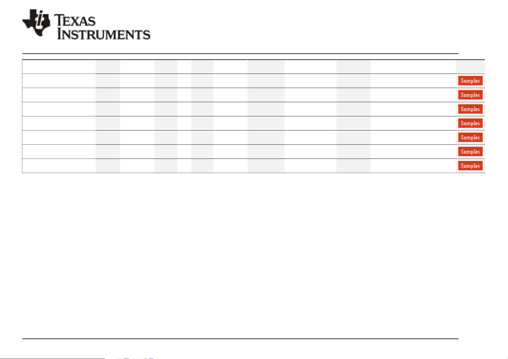
PACKAGE OPTION ADDENDUM
www.ti.com
Orderable Device Status
TPS65910A1RSLR ACTIVE VQFN RSL 48 2500 Green (RoHS
TPS65910A31A1RSLR ACTIVE VQFN RSL 48 2500 Green (RoHS
TPS65910A31A1RSLT ACTIVE VQFN RSL 48 250 Green (RoHS
TPS65910A3A1RSL ACTIVE VQFN RSL 48 60 Green (RoHS
TPS65910A3A1RSLR ACTIVE VQFN RSL 48 2500 Green (RoHS
TPS65910AA1RSL ACTIVE VQFN RSL 48 60 Green (RoHS
TPS65910AA1RSLR ACTIVE VQFN RSL 48 2500 Green (RoHS
(1)
The marketing status values are defined as follows:
ACTIVE: Product device recommended for new designs.
LIFEBUY: TI has announced that the device will be discontinued, and a lifetime-buy period is in effect.
NRND: Not recommended for new designs. Device is in production to support existing customers, but TI does not recommend using this part in a new design.
PREVIEW: Device has been announced but is not in production. Samples may or may not be available.
OBSOLETE: TI has discontinued the production of the device.
Package Type Package
(1)
Drawing
Pins Package
Qty
Eco Plan
(2)
& no Sb/Br)
& no Sb/Br)
& no Sb/Br)
& no Sb/Br)
& no Sb/Br)
& no Sb/Br)
& no Sb/Br)
Lead/Ball Finish MSL Peak Temp
(3)
CU NIPDAU Level-3-260C-168 HR -40 to 85 TPS
CU NIPDAU Level-3-260C-168 HR -40 to 85 65910
CU NIPDAU Level-3-260C-168 HR -40 to 85 65910
CU NIPDAU Level-3-260C-168 HR -40 to 85 T65910
CU NIPDAU Level-3-260C-168 HR -40 to 85 T65910
CU NIPDAU Level-3-260C-168 HR -40 to 85 T65910A
CU NIPDAU Level-3-260C-168 HR -40 to 85 T65910A
Op Temp (°C) Device Marking
(4/5)
65910A1
A31A1
A31A1
A3A1
A3A1
A1
A1
25-Sep-2013
(2)
Eco Plan - The planned eco-friendly classification: Pb-Free (RoHS), Pb-Free (RoHS Exempt), or Green (RoHS & no Sb/Br) - please check http://www.ti.com/productcontent for the latest availability
information and additional product content details.
TBD: The Pb-Free/Green conversion plan has not been defined.
Pb-Free (RoHS): TI's terms "Lead-Free" or "Pb-Free" mean semiconductor products that are compatible with the current RoHS requirements for all 6 substances, including the requirement that
lead not exceed 0.1% by weight in homogeneous materials. Where designed to be soldered at high temperatures, TI Pb-Free products are suitable for use in specified lead-free processes.
Pb-Free (RoHS Exempt): This component has a RoHS exemption for either 1) lead-based flip-chip solder bumps used between the die and package, or 2) lead-based die adhesive used between
the die and leadframe. The component is otherwise considered Pb-Free (RoHS compatible) as defined above.
Green (RoHS & no Sb/Br): TI defines "Green" to mean Pb-Free (RoHS compatible), and free of Bromine (Br) and Antimony (Sb) based flame retardants (Br or Sb do not exceed 0.1% by weight
in homogeneous material)
(3)
MSL, Peak Temp. -- The Moisture Sensitivity Level rating according to the JEDEC industry standard classifications, and peak solder temperature.
(4)
There may be additional marking, which relates to the logo, the lot trace code information, or the environmental category on the device.
(5)
Multiple Device Markings will be inside parentheses. Only one Device Marking contained in parentheses and separated by a "~" will appear on a device. If a line is indented then it is a continuation
of the previous line and the two combined represent the entire Device Marking for that device.
Samples
Addendum-Page 2

PACKAGE OPTION ADDENDUM
www.ti.com
25-Sep-2013
Important Information and Disclaimer:The information provided on this page represents TI's knowledge and belief as of the date that it is provided. TI bases its knowledge and belief on information
provided by third parties, and makes no representation or warranty as to the accuracy of such information. Efforts are underway to better integrate information from third parties. TI has taken and
continues to take reasonable steps to provide representative and accurate information but may not have conducted destructive testing or chemical analysis on incoming materials and chemicals.
TI and TI suppliers consider certain information to be proprietary, and thus CAS numbers and other limited information may not be available for release.
In no event shall TI's liability arising out of such information exceed the total purchase price of the TI part(s) at issue in this document sold by TI to Customer on an annual basis.
Addendum-Page 3

PACKAGE MATERIALS INFORMATION
www.ti.com 23-Sep-2013
TAPE AND REEL INFORMATION
*All dimensions are nominal
Device Package
TPS659101A1RSLR VQFN RSL 48 2500 330.0 16.4 6.3 6.3 1.1 12.0 16.0 Q2
TPS659102A1RSLR VQFN RSL 48 2500 330.0 16.4 6.3 6.3 1.5 12.0 16.0 Q2
TPS659102A1RSLR VQFN RSL 48 2500 330.0 16.4 6.3 6.3 1.1 12.0 16.0 Q2
TPS659106A1RSLR VQFN RSL 48 2500 330.0 16.4 6.3 6.3 1.5 12.0 16.0 Q2
TPS659108A1RSLR VQFN RSL 48 2500 330.0 16.4 6.3 6.3 1.1 12.0 16.0 Q2
TPS659108A1RSLR VQFN RSL 48 2500 330.0 16.4 6.3 6.3 1.5 12.0 16.0 Q2
TPS659109A1RSLR VQFN RSL 48 2500 330.0 16.4 6.3 6.3 1.1 12.0 16.0 Q2
TPS659109A1RSLR VQFN RSL 48 2500 330.0 16.4 6.3 6.3 1.5 12.0 16.0 Q2
TPS65910A1RSLR VQFN RSL 48 2500 330.0 16.4 6.3 6.3 1.5 12.0 16.0 Q2
TPS65910A31A1RSLR VQFN RSL 48 2500 330.0 16.4 6.3 6.3 1.5 12.0 16.0 Q2
TPS65910A31A1RSLT VQFN RSL 48 250 180.0 16.4 6.3 6.3 1.5 12.0 16.0 Q2
TPS65910A3A1RSLR VQFN RSL 48 2500 330.0 16.4 6.3 6.3 1.5 12.0 16.0 Q2
TPS65910AA1RSLR VQFN RSL 48 2500 330.0 16.4 6.3 6.3 1.1 12.0 16.0 Q2
TPS65910AA1RSLR VQFN RSL 48 2500 330.0 16.4 6.3 6.3 1.5 12.0 16.0 Q2
Type
Package
Drawing
Pins SPQ Reel
Diameter
(mm)
Reel
Width
W1 (mm)
A0
(mm)B0(mm)K0(mm)P1(mm)W(mm)
Quadrant
Pin1
Pack Materials-Page 1

PACKAGE MATERIALS INFORMATION
www.ti.com 23-Sep-2013
*All dimensions are nominal
Device Package Type Package Drawing Pins SPQ Length (mm) Width (mm) Height (mm)
TPS659101A1RSLR VQFN RSL 48 2500 367.0 367.0 38.0
TPS659102A1RSLR VQFN RSL 48 2500 367.0 367.0 38.0
TPS659102A1RSLR VQFN RSL 48 2500 367.0 367.0 38.0
TPS659106A1RSLR VQFN RSL 48 2500 367.0 367.0 38.0
TPS659108A1RSLR VQFN RSL 48 2500 367.0 367.0 38.0
TPS659108A1RSLR VQFN RSL 48 2500 367.0 367.0 38.0
TPS659109A1RSLR VQFN RSL 48 2500 367.0 367.0 38.0
TPS659109A1RSLR VQFN RSL 48 2500 367.0 367.0 38.0
TPS65910A1RSLR VQFN RSL 48 2500 367.0 367.0 38.0
TPS65910A31A1RSLR VQFN RSL 48 2500 367.0 367.0 38.0
TPS65910A31A1RSLT VQFN RSL 48 250 210.0 185.0 35.0
TPS65910A3A1RSLR VQFN RSL 48 2500 367.0 367.0 38.0
TPS65910AA1RSLR VQFN RSL 48 2500 367.0 367.0 38.0
TPS65910AA1RSLR VQFN RSL 48 2500 367.0 367.0 38.0
Pack Materials-Page 2


IMPORTANT NOTICE
Texas Instruments Incorporated and its subsidiaries (TI) reserve the right to make corrections, enhancements, improvements and other
changes to its semiconductor products and services per JESD46, latest issue, and to discontinue any product or service per JESD48, latest
issue. Buyers should obtain the latest relevant information before placing orders and should verify that such information is current and
complete. All semiconductor products (also referred to herein as “components”) are sold subject to TI’s terms and conditions of sale
supplied at the time of order acknowledgment.
TI warrants performance of its components to the specifications applicable at the time of sale, in accordance with the warranty in TI’s terms
and conditions of sale of semiconductor products. Testing and other quality control techniques are used to the extent TI deems necessary
to support this warranty. Except where mandated by applicable law, testing of all parameters of each component is not necessarily
performed.
TI assumes no liability for applications assistance or the design of Buyers’ products. Buyers are responsible for their products and
applications using TI components. To minimize the risks associated with Buyers’ products and applications, Buyers should provide
adequate design and operating safeguards.
TI does not warrant or represent that any license, either express or implied, is granted under any patent right, copyright, mask work right, or
other intellectual property right relating to any combination, machine, or process in which TI components or services are used. Information
published by TI regarding third-party products or services does not constitute a license to use such products or services or a warranty or
endorsement thereof. Use of such information may require a license from a third party under the patents or other intellectual property of the
third party, or a license from TI under the patents or other intellectual property of TI.
Reproduction of significant portions of TI information in TI data books or data sheets is permissible only if reproduction is without alteration
and is accompanied by all associated warranties, conditions, limitations, and notices. TI is not responsible or liable for such altered
documentation. Information of third parties may be subject to additional restrictions.
Resale of TI components or services with statements different from or beyond the parameters stated by TI for that component or service
voids all express and any implied warranties for the associated TI component or service and is an unfair and deceptive business practice.
TI is not responsible or liable for any such statements.
Buyer acknowledges and agrees that it is solely responsible for compliance with all legal, regulatory and safety-related requirements
concerning its products, and any use of TI components in its applications, notwithstanding any applications-related information or support
that may be provided by TI. Buyer represents and agrees that it has all the necessary expertise to create and implement safeguards which
anticipate dangerous consequences of failures, monitor failures and their consequences, lessen the likelihood of failures that might cause
harm and take appropriate remedial actions. Buyer will fully indemnify TI and its representatives against any damages arising out of the use
of any TI components in safety-critical applications.
In some cases, TI components may be promoted specifically to facilitate safety-related applications. With such components, TI’s goal is to
help enable customers to design and create their own end-product solutions that meet applicable functional safety standards and
requirements. Nonetheless, such components are subject to these terms.
No TI components are authorized for use in FDA Class III (or similar life-critical medical equipment) unless authorized officers of the parties
have executed a special agreement specifically governing such use.
Only those TI components which TI has specifically designated as military grade or “enhanced plastic” are designed and intended for use in
military/aerospace applications or environments. Buyer acknowledges and agrees that any military or aerospace use of TI components
which have not been so designated is solely at the Buyer's risk, and that Buyer is solely responsible for compliance with all legal and
regulatory requirements in connection with such use.
TI has specifically designated certain components as meeting ISO/TS16949 requirements, mainly for automotive use. In any case of use of
non-designated products, TI will not be responsible for any failure to meet ISO/TS16949.
Products Applications
Audio www.ti.com/audio Automotive and Transportation www.ti.com/automotive
Amplifiers amplifier.ti.com Communications and Telecom www.ti.com/communications
Data Converters dataconverter.ti.com Computers and Peripherals www.ti.com/computers
DLP® Products www.dlp.com Consumer Electronics www.ti.com/consumer-apps
DSP dsp.ti.com Energy and Lighting www.ti.com/energy
Clocks and Timers www.ti.com/clocks Industrial www.ti.com/industrial
Interface interface.ti.com Medical www.ti.com/medical
Logic logic.ti.com Security www.ti.com/security
Power Mgmt power.ti.com Space, Avionics and Defense www.ti.com/space-avionics-defense
Microcontrollers microcontroller.ti.com Video and Imaging www.ti.com/video
RFID www.ti-rfid.com
OMAP Applications Processors www.ti.com/omap TI E2E Community e2e.ti.com
Wireless Connectivity www.ti.com/wirelessconnectivity
Mailing Address: Texas Instruments, Post Office Box 655303, Dallas, Texas 75265
Copyright © 2013, Texas Instruments Incorporated

 Loading...