

Page 1

User's Guide
SLVUA85–June 2014
TPS65261EVM-650 PMIC 3-A, 2-A, 2-A Output Current
Evaluation Module
This document presents the information required to operate the TPS65261 PMIC as well as the support
documentation including schematic, layout, hardware setup, and bill of materials (BOM).
Contents
1 Background................................................................................................................... 2
2 TPS65261 Schematic ....................................................................................................... 3
3 Board Layout ................................................................................................................. 4
4 Bench Test Setup Conditions .............................................................................................. 6
5 Power-Up Procedure........................................................................................................ 7
6 Bill of Materials............................................................................................................... 8
List of Figures
1 TPS65261 Schematic ....................................................................................................... 3
2 Component Placement (Top Layer)....................................................................................... 4
3 Board Layout (Top Layer) .................................................................................................. 5
4 Board Layout (Second Layer).............................................................................................. 5
5 Board Layout (Third Layer)................................................................................................. 5
6 Board Layout (Bottom Layer) .............................................................................................. 5
7 Header Descriptions and Jumper Placement ............................................................................ 6
SLVUA85–June 2014 TPS65261EVM-650 PMIC 3-A, 2-A, 2-A Output Current Evaluation Module
Submit Documentation Feedback
1
Copyright © 2014, Texas Instruments Incorporated
Page 2
Background
1 Background
The TPS65261 PMIC is a triple 3-A, 2-A, 2-A output current, synchronous step-down (buck) converter with
an operational range of 4.5 V to 18 V. The TPS65261 features an automatic power sequence with
connecting MODE pin to V7V and configuring EN1/2/3 pins. The device also features an open drain
RESET signal to monitor power down. The TPS65261 operates in pulse skipping mode (PSM) light load.
As there are many possible options to set the converters, Table 1 presents the performance specification
summary for the EVM.
This evaluation module is designed to provide access to the features of the TPS65261. Some
modifications can be made to this module to test performance at different input and output voltages,
current and switching frequency. Contact the TI Field Applications group for advice on these matters.
www.ti.com
Table 1. Summary of Performance
Test Conditions Performance
VIN = 4.5 V to 18 V BUCK1, 1.2 V, up to 3 A
fSW= 600 kHz BUCK2, 3.3 V, up to 2 A
(25°C ambient) BUCK3, 1.8 V, up to 2 A
RESET, pull low when VDIV lower than 1.23 V
All trademarks are the property of their respective owners.
2
TPS65261EVM-650 PMIC 3-A, 2-A, 2-A Output Current Evaluation Module SLVUA85–June 2014
Copyright © 2014, Texas Instruments Incorporated
Submit Documentation Feedback
Page 3
0.047µF
C11
10µF
C9
82pF
C5
0.01µF
C17
3300pF
C6
22pF
C4
0
R8
20.0k
R3
22pF
C15
1µF
C10
4.7µH
L2
1
2
3
J5
22µF
C12
GND
GND
GND
GND
GND
1
2
3
J8100k
R21
51k
R25
GND
10µFC710µF
C8
0
R10
DNI
TP11
0.047µF
C18
0
R15
4.7µH
L3
22µF
C21
GND
0
R16
DNI
TP14
22pF
C25
GND
4.7µH
L1
22µF
C3
22µF
C2
0
R2
GND
0.047µF
C1
0
R1
GND
1
2
J3
GND
TP12
TP13
EN1
EN2
EN3
MODE
1
2
J2
GND
TP6
TP15
1
2
J1
GND
TP1
TP3
DNI
TP4
EN1 MODE
GND GND
1
2
J4
GND
TP2
TP5
VIN
VIN
10.0k
R5
10.0k
R6
10.0k
R13
DNI
C26
VOUT1 1.2V 3A
VOUT2 3.3V 2A
VOUT3 1.8V 2A
VIN 12V
GND
VFB1
VFB1
22µF
C13
GND
VFB2
VFB2
VFB3
22pF
C14
GND
22µF
C22
GND
VFB3
22pF
C23
GND
GND
0.01µF
C19
0.01µF
C20
GND
73.2k
R17
20.0k
R7
GND
100k
R11
TP9
TP8
100k
R9
V7V
V7V
1
2
3
J6100k
R22
51k
R26
GND
EN2
GND
DNI
C27
1
2
3
J7100k
R23
51k
R27
GND
EN3
GND
DNI
C28
V7V
GND
10.0k
R19
20.0k
R20
45.3k
R14
30k
R12
30k
R18
2200pF
C16
2200pF
C24
147k
R4
TP7
GND
TP10
PGOOD
2
MODE
4
FB2
6
EN2
32
BST2
9
LX2
10
PGND2
11
PVIN2
12
PVIN3
13
PGND3
14
LX3
15
BST3
16
FB3
19
AGND
21
V7V
5
COMP1
23
SS1
24
FB1
22
EN1
31
BST1
25
LX1
26
PGND1
27
PVIN1
28
VDIV
30
PAD
RESET
3
COMP2
7
COMP3
18
SS2
8
SS3
17
ROSC
20
VIN
29
EN3
1
U1
TPS65261RHB
VDIV
VDIV
www.ti.com
TPS65261 Schematic
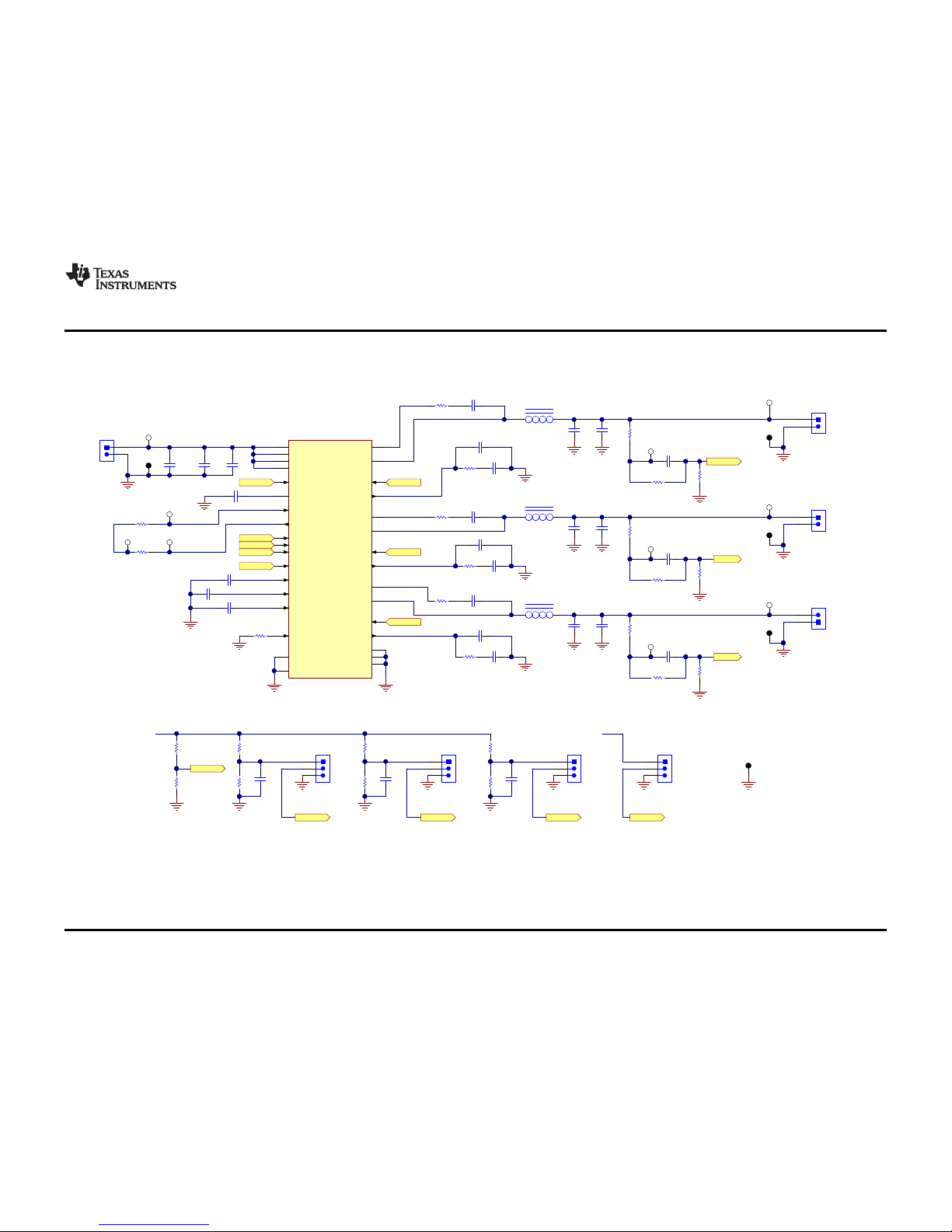
2 TPS65261 Schematic
Figure 1 shows the EVM schematic.
Figure 1. TPS65261 Schematic
3
SLVUA85–June 2014 TPS65261EVM-650 PMIC 3-A, 2-A, 2-A Output Current Evaluation Module
Submit Documentation Feedback
Copyright © 2014, Texas Instruments Incorporated
Page 4

Board Layout
3 Board Layout
Figure 2 illustrates the PCB layout for this EVM.
www.ti.com
Figure 2. Component Placement (Top Layer)
4
TPS65261EVM-650 PMIC 3-A, 2-A, 2-A Output Current Evaluation Module SLVUA85–June 2014
Copyright © 2014, Texas Instruments Incorporated
Submit Documentation Feedback
Page 5

www.ti.com
3.1 EVM Layout
Figure 3 through Figure 6 illustrate the PCB layout for this EVM.
Board Layout
Figure 3. Board Layout (Top Layer) Figure 4. Board Layout (Second Layer)
Figure 5. Board Layout (Third Layer) Figure 6. Board Layout (Bottom Layer)
SLVUA85–June 2014 TPS65261EVM-650 PMIC 3-A, 2-A, 2-A Output Current Evaluation Module
Submit Documentation Feedback
5
Copyright © 2014, Texas Instruments Incorporated
Page 6

Bench Test Setup Conditions
4 Bench Test Setup Conditions
4.1 Headers Description and Jumper Placement
Figure 7 illustrates the header description and jumper placement on the EVM.
www.ti.com
Figure 7. Header Descriptions and Jumper Placement
Test points:
A: LX of VOUT1
B: LX of VOUT2
C: LX of VOUT3
VOUT1, VOUT2, VOUT3, VIN, PGOOD, RESET, V7V
6
TPS65261EVM-650 PMIC 3-A, 2-A, 2-A Output Current Evaluation Module SLVUA85–June 2014
Copyright © 2014, Texas Instruments Incorporated
Submit Documentation Feedback
Page 7
www.ti.com
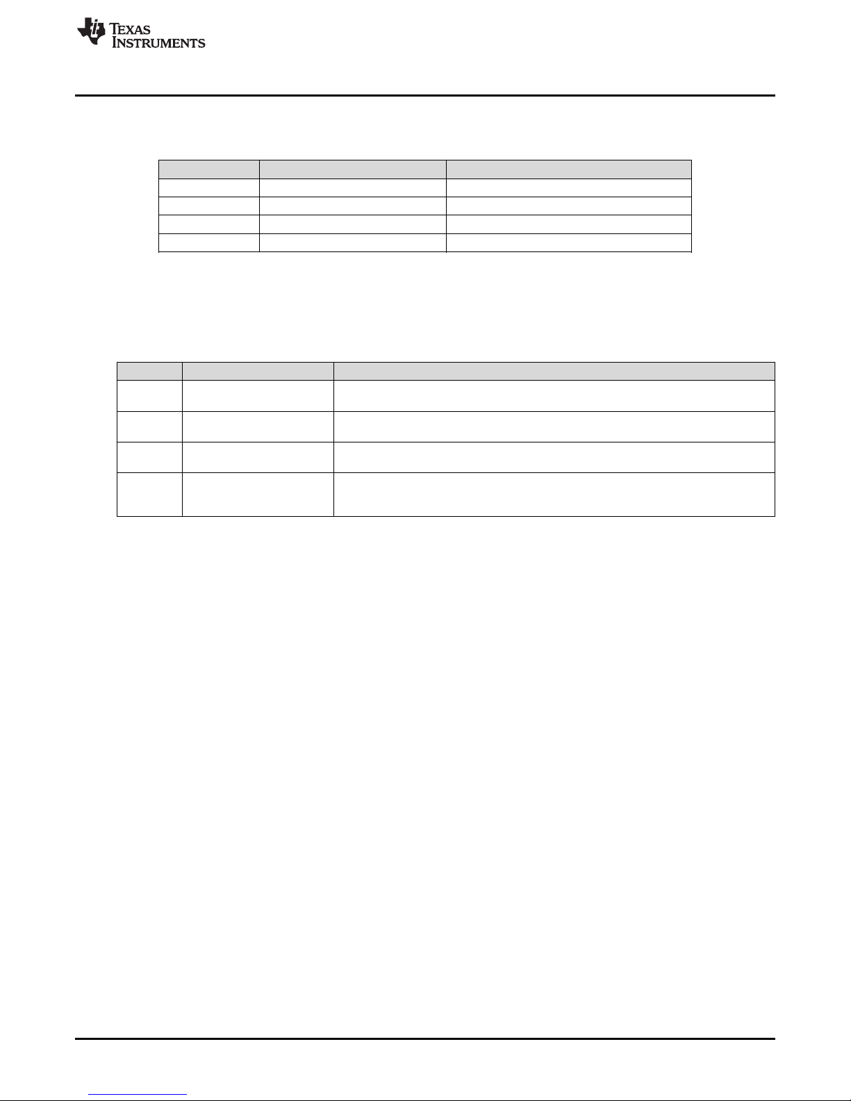
Table 2 lists the I/O connections.
Number Function Description
J1 BUCK1 connector Output of BUCK1
J2 BUCK2 connector Output of BUCK2
J3 BUCK3 connector Output of BUCK3
J4 VIN connector Apply power supply to this connector
4.2 Jumpers and Switches
Table 3 lists the jumpers on the EVM.
Jumper Function Placement
J5 Buck1 enable (EN1) Connect EN1 to GND to disable VOUT1, connect EN1 to VIN through a 100-kΩ
J6 Buck2 enable (EN2) Connect EN2 to GND to disable VOUT2, connect EN2 to VIN through a 100-kΩ
J7 Buck3 enable (EN3) Connect EN3 to GND to disable VOUT3, connect EN3 to VIN through a 100-kΩ
J8 Mode Power sequencing mode control pin. Connect this pin to GND to set power sequence
Bench Test Setup Conditions
Table 2. Input/Output Connection
Table 3. Jumpers
resistor to enable VOUT1; leave open to enable VOUT1
resistor to enable VOUT2; leave open to enable VOUT2
resistor to enable VOUT3; leave open to enable VOUT3
with dedicated enable pin; connect this pin to V7V, set the power sequence with the
pre-defined power up and power down sequence.
5 Power-Up Procedure
Power sequence with dedicated enable pin:
1. Connect J8 to GND
2. Apply 4.5 V - 18 V to J4
3. Toggle J5, J6, or J7 to enable VOUT1, VOUT2, and VOUT3, respectively
4. Apply loads to the output connectors
Power sequence with the pre-defined power up and power down sequence:
1. Connect J8 to V7V
2. Connect J5 to High (or Low), J6 to High (or Low)
3. Apply 4.5 V - 18 V to J4
4. Toggle J7 to enable VOUT1, VOUT2, and VOUT3
5. Apply loads to the output connectors.
SLVUA85–June 2014 TPS65261EVM-650 PMIC 3-A, 2-A, 2-A Output Current Evaluation Module
Submit Documentation Feedback
7
Copyright © 2014, Texas Instruments Incorporated
Page 8

Bill of Materials
www.ti.com
6 Bill of Materials
Table 4 lists the BOM for this EVM.
Table 4. TPS65261 Bill of Materials
Designator Qty Value Description Package Reference Part Number Manufacturer
!PCB1 1 Printed Circuit Board PWR650 Any
C1, C11, C18 3 0.047uF CAP, CERM, 0.047uF, 50V, +/-10%, X7R, 0603 0603 C1608X7R1H473K TDK
C2, C3, C12, C13, C21, 6 22uF CAP, CERM, 22uF, 16V, +/-20%, X5R, 1206 1206 1206YD226MAT2A AVX
C22
C4, C14, C15, C23, C25 5 22pF CAP, CERM, 22pF, 50V, +/-5%, C0G/NP0, 0603 0603 06035A220JAT2A AVX
C5 1 82pF CAP,CERM, 82pF, 50V, +/-5%, C0G/NP0, 0603 0603 06035A820JAT2A AVX
C6 1 3300pF CAP, CERM, 3300pF, 50V, +/-10%, X7R, 0603 0603 C0603C332K5RACTU Kemet
C7, C8, C9 3 10uF CAP, CERM, 10uF, 25V, +/-10%, X5R, 1206 1206 GRM31CR61E106KA12L MuRata
C10 1 1uF CAP,CERM, 1uF, 25V, +/-10%, X7R, 0603 0603 C1608X7R1E105K080AB TDK
C16, C24 2 2200pF CAP, CERM, 2200pF, 50V, +/-10%, X7R, 0603 0603 C0603C222K5RACTU Kemet
C17, C19, C20 3 0.01uF CAP, CERM, 0.01uF, 50V, +/-5%, X7R, 0603 0603 C0603C103J5RACTU Kemet
C26, C27, C28 0 DNI CAP, CERM, 0.01uF, 50V, +/-5%, X7R, 0603 0603 C0603C103J5RACTU Kemet
J1, J2, J3, J4 4 Terminal Block, 6A, 3.5mm Pitch, 2-Pos, TH 7.0x8.2x6.5mm ED555/2DS On-Shore Technology
J5, J6, J7, J8 4 Header, 100mil, 3x1, Tin plated, TH Header, 3 PIN, 100mil, Tin PEC03SAAN Sullins Connector Solutions
L1, L2, L3 3 4.7uH Inductor, Shielded Drum Core, Superflux, 4.7uH, 6A, 0.02 ohm, SMD WE-HC4 744311470 Wurth Elektronik eiSos
LBL1 1 Thermal Transfer Printable Labels, 0.650" W x 0.200" H - 10,000 per roll PCB Label 0.650"H x 0.200"W THT-14-423-10 Brady
R1, R2, R8, R10, R15, 6 0 RES, 0 ohm, 5%, 0.1W, 0603 0603 CRCW06030000Z0EA Vishay-Dale
R16
R3, R7, R20 3 20.0k RES,20.0k ohm, 1%, 0.1W, 0603 0603 CRCW060320K0FKEA Vishay-Dale
R4 1 147k RES, 147k ohm, 1%, 0.1W, 0603 0603 CRCW0603147KFKEA Vishay-Dale
R5, R6, R13, R19 4 10.0k RES, 10.0k ohm, 1%, 0.1W, 0603 0603 CRCW060310K0FKEA Vishay-Dale
R9, R11, R21, R22, R23 5 100k RES, 100k ohm, 1%, 0.1W, 0603 0603 CRCW0603100KFKEA Vishay-Dale
R12, R18 2 30k RES, 30k ohm, 5%, 0.1W, 0603 0603 CRCW060330K0JNEA Vishay-Dale
R14 1 45.3k RES, 45.3k ohm, 1%, 0.1W, 0603 0603 CRCW060345K3FKEA Vishay-Dale
R17 1 73.2k RES, 73.2k ohm, 1%, 0.1W, 0603 0603 CRCW060373K2FKEA Vishay-Dale
R25, R26, R27 3 51k RES, 51k ohm, 5%, 0.1W, 0603 0603 CRCW060351K0JNEA Vishay-Dale
SH-J1 1 1x2 Shunt, 100mil, Gold plated, Black Shunt 969102-0000-DA 3M
TP1, TP2, TP6, TP7, 7 White Test Point, Miniature, White, TH White Miniature Testpoint 5002 Keystone
TP8, TP9, TP12
TP3, TP5, TP10, TP13, 5 Black Test Point, Miniature, Black, TH Black Miniature Testpoint 5001 Keystone
TP15
TP4, TP11, TP14 0 DNI Test Point, Miniature, White, TH White Miniature Testpoint 5002 Keystone
U1 1 4.5Vto 18V Input Voltage, 3A/2A/2A Output Current Triple Synchronous Step- RHB0032E TPS65261RHB Texas Instruments
Down Converter, RHB0032E
Note: Unless otherwise noted in the columns, all parts may be substituted with equivalents.
8
TPS65261EVM-650 PMIC 3-A, 2-A, 2-A Output Current Evaluation Module SLVUA85–June 2014
Submit Documentation Feedback
Copyright © 2014, Texas Instruments Incorporated
Page 9

IMPORTANT NOTICE
Texas Instruments Incorporated and its subsidiaries (TI) reserve the right to make corrections, enhancements, improvements and other
changes to its semiconductor products and services per JESD46, latest issue, and to discontinue any product or service per JESD48, latest
issue. Buyers should obtain the latest relevant information before placing orders and should verify that such information is current and
complete. All semiconductor products (also referred to herein as “components”) are sold subject to TI’s terms and conditions of sale
supplied at the time of order acknowledgment.
TI warrants performance of its components to the specifications applicable at the time of sale, in accordance with the warranty in TI’s terms
and conditions of sale of semiconductor products. Testing and other quality control techniques are used to the extent TI deems necessary
to support this warranty. Except where mandated by applicable law, testing of all parameters of each component is not necessarily
performed.
TI assumes no liability for applications assistance or the design of Buyers’ products. Buyers are responsible for their products and
applications using TI components. To minimize the risks associated with Buyers’ products and applications, Buyers should provide
adequate design and operating safeguards.
TI does not warrant or represent that any license, either express or implied, is granted under any patent right, copyright, mask work right, or
other intellectual property right relating to any combination, machine, or process in which TI components or services are used. Information
published by TI regarding third-party products or services does not constitute a license to use such products or services or a warranty or
endorsement thereof. Use of such information may require a license from a third party under the patents or other intellectual property of the
third party, or a license from TI under the patents or other intellectual property of TI.
Reproduction of significant portions of TI information in TI data books or data sheets is permissible only if reproduction is without alteration
and is accompanied by all associated warranties, conditions, limitations, and notices. TI is not responsible or liable for such altered
documentation. Information of third parties may be subject to additional restrictions.
Resale of TI components or services with statements different from or beyond the parameters stated by TI for that component or service
voids all express and any implied warranties for the associated TI component or service and is an unfair and deceptive business practice.
TI is not responsible or liable for any such statements.
Buyer acknowledges and agrees that it is solely responsible for compliance with all legal, regulatory and safety-related requirements
concerning its products, and any use of TI components in its applications, notwithstanding any applications-related information or support
that may be provided by TI. Buyer represents and agrees that it has all the necessary expertise to create and implement safeguards which
anticipate dangerous consequences of failures, monitor failures and their consequences, lessen the likelihood of failures that might cause
harm and take appropriate remedial actions. Buyer will fully indemnify TI and its representatives against any damages arising out of the use
of any TI components in safety-critical applications.
In some cases, TI components may be promoted specifically to facilitate safety-related applications. With such components, TI’s goal is to
help enable customers to design and create their own end-product solutions that meet applicable functional safety standards and
requirements. Nonetheless, such components are subject to these terms.
No TI components are authorized for use in FDA Class III (or similar life-critical medical equipment) unless authorized officers of the parties
have executed a special agreement specifically governing such use.
Only those TI components which TI has specifically designated as military grade or “enhanced plastic” are designed and intended for use in
military/aerospace applications or environments. Buyer acknowledges and agrees that any military or aerospace use of TI components
which have not been so designated is solely at the Buyer's risk, and that Buyer is solely responsible for compliance with all legal and
regulatory requirements in connection with such use.
TI has specifically designated certain components as meeting ISO/TS16949 requirements, mainly for automotive use. In any case of use of
non-designated products, TI will not be responsible for any failure to meet ISO/TS16949.
Products Applications
Audio www.ti.com/audio Automotive and Transportation www.ti.com/automotive
Amplifiers amplifier.ti.com Communications and Telecom www.ti.com/communications
Data Converters dataconverter.ti.com Computers and Peripherals www.ti.com/computers
DLP® Products www.dlp.com Consumer Electronics www.ti.com/consumer-apps
DSP dsp.ti.com Energy and Lighting www.ti.com/energy
Clocks and Timers www.ti.com/clocks Industrial www.ti.com/industrial
Interface interface.ti.com Medical www.ti.com/medical
Logic logic.ti.com Security www.ti.com/security
Power Mgmt power.ti.com Space, Avionics and Defense www.ti.com/space-avionics-defense
Microcontrollers microcontroller.ti.com Video and Imaging www.ti.com/video
RFID www.ti-rfid.com
OMAP Applications Processors www.ti.com/omap TI E2E Community e2e.ti.com
Wireless Connectivity www.ti.com/wirelessconnectivity
Mailing Address: Texas Instruments, Post Office Box 655303, Dallas, Texas 75265
Copyright © 2014, Texas Instruments Incorporated
 Loading...