

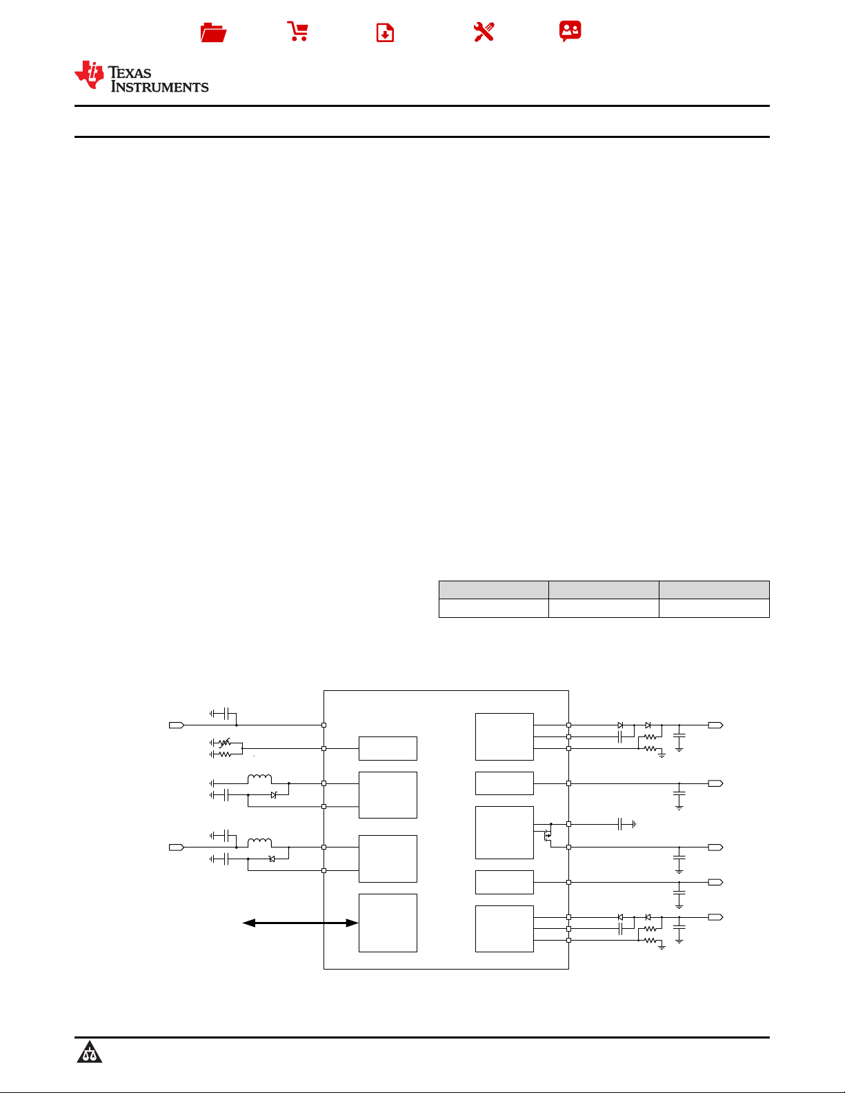
VIN
I/O Control
From Input
Supply
(3.0 V-6.0 V)
Temp
Sensor
TS
DCDC2
VN
VN_SW
DCDC1
VB_SW
VB
From Input
Supply
(3.0 V-6.0 V)
VDDH_D
VDDH_DRV
VDDH_FB
Positive
Charge
Pump
VPOS
LDO1
VEE_D
VEE_DRV
VEE_FB
Negative
Charge
Pump
VCOM
VCOM
VCOM_PANEL
VNEG
LDO2
VCOM
Product
Folder
Sample &
Buy
Technical
Documents
Tools &
Software
Support &
Community
SLVSB04A –JULY 2011–REVISED AUGUST 2015
TPS65186 PMIC for E Ink®Vizplex™ Enabled Electronic Paper Display
1 Features 2 Applications
1
• Single Chip Power-Management Solution for
E Ink®Vizplex™ Electronic Paper Displays Panels
• Generates Positive and Negative Gates, Source • EPD Power Supplies
Driver Voltages, and Back-Plane Bias From a
Single, Low-Voltage Input Supply
• Supports 9.7 Inch and Larger Panel Size
• 3-V to 6-V Input Voltage Range
• Boost Converter for Positive Rail Base
• Inverting Buck-Boost Converter for Negative Rail Software Timing Controller (OMAP™)
Base
• Two Adjustable LDOs for Source Driver Supply
– LDO1: 15 V, 120 mA (VPOS)
– LDO2: –15 V, 120 mA (VNEG)
• Accurate Output Voltage Tracking
– VPOS – VNEG = ±50 mV
• Two Charge Pumps for Gate Driver Supply
– CP1: 22 V, 10 mA (VDDH)
– CP2: –20 V, 12 mA, (VEE)
• Adjustable VCOM Driver for Accurate PanelBackplane Biasing
– 0 V to –5.11 V
– ± 1.5% accuracy (±10 mV)
– 9-Bit Control (10-mV Nominal Step Size)
• Integrated 10-Ω, 3.3-V Power Switch for Disabling
System Power Rail to E-Ink Panel
• Power Supply for Active Matrix E Ink Vizplex
• E-Book Readers
• EPSON®S1D13522 (ISIS) Timing Controller
• EPSON®S1D13521 (Broadsheet) Timing
Controller
• Application Processors With Integrated or
3 Description
The TPS65186 device is a single-chip power supply
designed to for E Ink Vizplex displays used in
portable e-reader applications, and the device
supports panel sizes up to 9.7 inches and greater.
Two high-efficiency DC-DC boost converters
generate ±16-V rails that are boosted to 22 V and
–20 V by two change pumps to provide the gate
driver supply for the Vizplex panel. Two tracking
LDOs create the ±15-V source driver supplies that
support up to 120-mA of output current. All rails are
adjustable through the I2C interface to accommodate
specific panel requirements.
Device Information
PART NUMBER PACKAGE BODY SIZE (NOM)
TPS65186 VQFN (48) 7.00 mm × 7.00 mm
(1) For all available packages, see the orderable addendum at
the end of the data sheet.
(1)
TPS65186
Typical Application Schematic
1
An IMPORTANT NOTICE at the end of this data sheet addresses availability, warranty, changes, use in safety-critical applications,
intellectual property matters and other important disclaimers. PRODUCTION DATA.
TPS65186
SLVSB04A –JULY 2011–REVISED AUGUST 2015
www.ti.com
Table of Contents
1 Features.................................................................. 1
2 Applications ........................................................... 1
3 Description ............................................................. 1
4 Revision History..................................................... 2
5 Description (continued)......................................... 3
6 Pin Configuration and Functions......................... 3
7 Specifications......................................................... 5
7.1 Absolute Maximum Ratings ...................................... 5
7.2 ESD Ratings.............................................................. 5
7.3 Recommended Operating Conditions....................... 5
7.4 Thermal Information.................................................. 6
7.5 Electrical Characteristics........................................... 6
7.6 Timing Requirements: Data Transmission.............. 10
7.7 Typical Characteristics............................................ 12
8 Detailed Description............................................ 15
8.1 Overview ................................................................. 15
8.2 Functional Block Diagram....................................... 16
8.3 Feature Description................................................. 17
8.4 Device Functional Modes........................................ 24
8.5 Programming........................................................... 26
8.6 Register Maps......................................................... 27
9 Application and Implementation ........................ 44
9.1 Application Information............................................ 44
9.2 Typical Application ................................................. 44
10 Power Supply Recommendations ..................... 46
11 Layout................................................................... 46
11.1 Layout Guidelines ................................................. 46
11.2 Layout Example .................................................... 46
12 Device and Documentation Support................. 47
12.1 Device Support...................................................... 47
12.2 Community Resources.......................................... 47
12.3 Trademarks........................................................... 47
12.4 Electrostatic Discharge Caution............................ 47
12.5 Glossary................................................................ 47
13 Mechanical, Packaging, and Orderable
Information........................................................... 47
4 Revision History
NOTE: Page numbers for previous revisions may differ from page numbers in the current version.
Changes from Original (July 2011) to Revision A Page
• Added ESD Ratings table, Feature Description section, Device Functional Modes, Application and Implementation
section, Power Supply Recommendations section, Layout section, Device and Documentation Support section, and
Mechanical, Packaging, and Orderable Information section.................................................................................................. 1
• Changed R
from “TBD” to “5 Ω”........................................................................................................................................ 8
OUT
2 Submit Documentation Feedback Copyright © 2011–2015, Texas Instruments Incorporated
Product Folder Links: TPS65186
VREF – 1
nINT – 2
VNEG – 3
VNEG_IN – 4
WAKEUP – 5
DGND – 6
INT_LDO – 7
AGND1 – 8
N/C – 9
VIN – 10
N/C – 11
23 – PBKG
22 – PWRUP
21 – N/C
20 – N/C
19 – N/C
18 – SDA
17 – SCL
16 – VCOM_PWR
15 – N/C
14 – VCOM
13 – N/C
24 – PWR_GOODVDDH_IN – 37
N/C – 38
N/C – 39
VB_SW – 40
PGND1 – 41
VB – 42
VPOS_IN – 43
VPOS – 44
VIN3P3 – 45
V3P3 – 46
TS – 47
AGND2 – 48
36 – VDDH_DRV
26 – N/C
35 – VDDH_D
34 – VDDH_FB
33 – PGND2
32 – VEE_FB
31 – VEE_D
27 – VIN_P
30 – VEE_DRV
29 – VEE_IN
28 – VN
25 – VN_SW
TPS65186
www.ti.com
SLVSB04A –JULY 2011–REVISED AUGUST 2015
5 Description (continued)
Accurate back-plane biasing is provided by a linear amplifier that can be adjusted from 0 V to –5.11 V with 9-bit
control through the serial interface; it can also source or sink current depending on panel condition. The
TPS65186 supports automatic panel kickback voltage measurement, which eliminates the need for manual
VCOM calibration in the production line. The measurement result can be stored in nonvolatile memory to become
the new VCOM power-up default value.
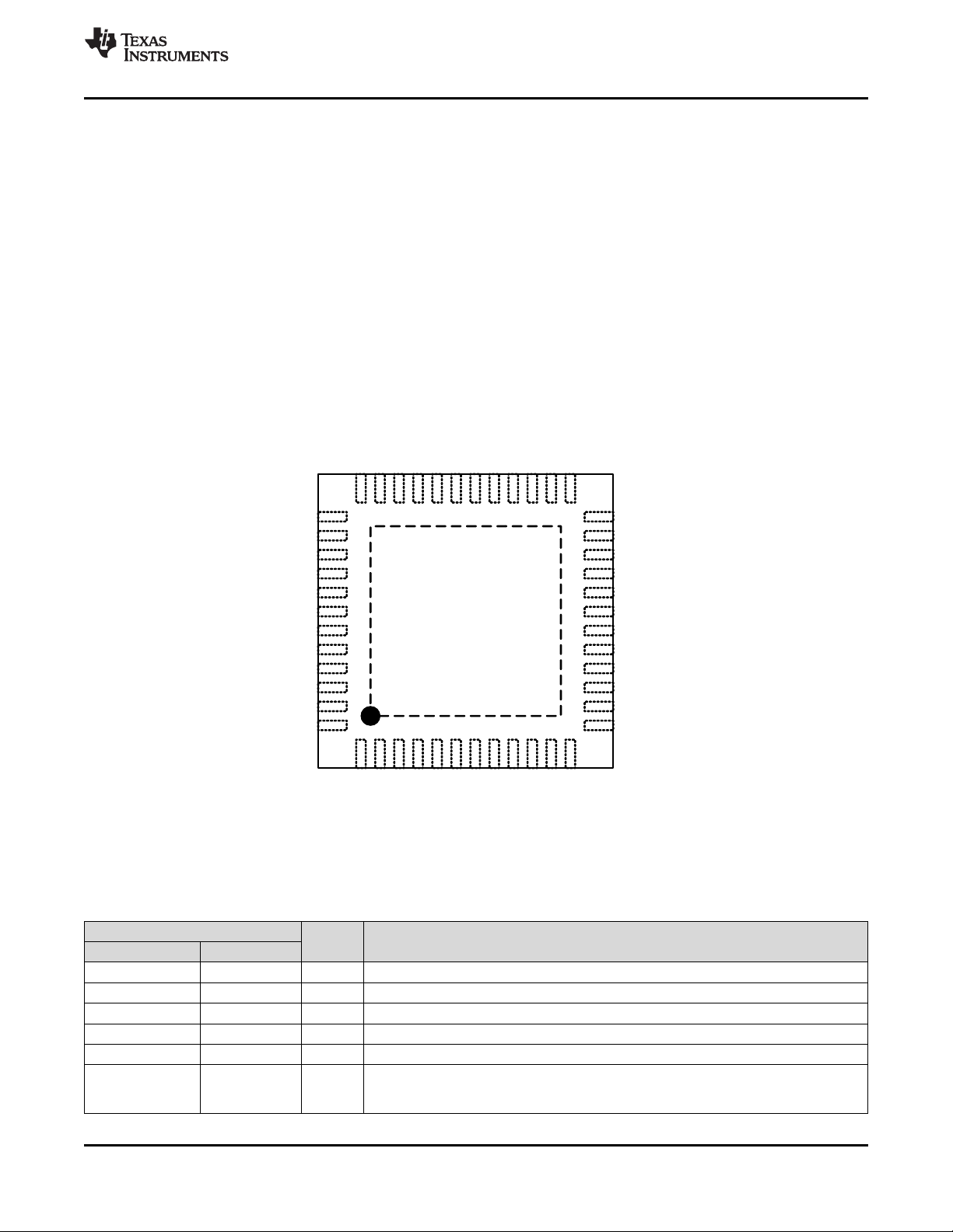
TPS65186 is available in a 48-pin 7-mm × 7-mm2VQFN with 0.5-mm pitch.
6 Pin Configuration and Functions
RGZ Package
48-Pin VQFN
Top View
PIN
NAME NO.
AGND1 8 — Analog ground for general analog circuitry
AGND2 48 — Reference point to external thermistor and linearization resistor
DGND 6 — Digital ground. Connect to ground plane.
INT_LDO 7 O Filter pin for 2.7-V internal supply
nINT 2 O Open drain interrupt pin (active low)
9, 11, 13, 15,
38, 39
N/C 19, 20, 21, 26, — Not internally connected
Copyright © 2011–2015, Texas Instruments Incorporated Submit Documentation Feedback 3
Pin Functions
I/O DESCRIPTION
Product Folder Links: TPS65186
TPS65186
SLVSB04A –JULY 2011–REVISED AUGUST 2015
Pin Functions (continued)
PIN
NAME NO.
PBKG 23 —
PGND1 41 — Power ground for DCDC1
PGND2 33 — Power ground for CP1 (VDDH) and CP2 (VEE) charge pumps
PWR_GOOD 24 O
PWRUP 22 I Power-up pin. Pull this pin high to power up all output rails.
SCL 17 I Serial interface (I2C) clock input
SDA 18 I/O Serial interface (I2C) data input/output
TS 47 I
V3P3 46 O Output pin of 3.3-V power switch
VB 42 I
VB_SW 40 O Boost converter switch out (DCDC1)
VCOM 14 I Filter pin for panel common-voltage driver
VCOM_CTRL 12 I
VCOM_PWR 16 I Internal supply input pin to VCOM buffer. Connect to the output of DCDC2.
VDDH_D 35 O Base voltage output pin for positive charge pump (CP1)
VDDH_DRV 36 O Driver output pin for positive charge pump (CP1)
VDDH_FB 34 I Feedback pin for positive charge pump (CP1)
VDDH_IN 37 I Input supply pin for positive charge pump (CP1)
VEE_D 31 I Base voltage output pin for negative charge pump (CP2)
VEE_DRV 30 O Driver output pin for negative charge pump (CP2)
VEE_FB 32 I Feedback pin for negative charge pump (CP2)
VEE_IN 29 I Input supply pin for negative charge pump (CP2) (VEE)
VIN 10 I Input power supply to general circuitry
VIN3P3 45 I Input pin to 3.3-V power switch
VIN_P 27 I Input power supply to inverting buck-boost converter (DCDC2)
VN 28 I
VNEG 3 O Negative supply output pin for panel source drivers
VNEG_IN 4 I Input pin for LDO2 (VNEG)
VN_SW 25 O Inverting buck-boost converter switch out (DCDC2)
VREF 1 O Filter pin for 2.25-V internal reference to ADC
VPOS 44 O Positive supply output pin for panel source drivers
VPOS_IN 43 I Input pin for LDO1 (VPOS)
WAKEUP 5 I commands after WAKEUP pin is pulled high but power rails remain disabled until
PowerPad — —
(1) There will be 0-ns of deglitch for PWRx.
(2) There will be 62.52-µs of deglitch for VCOM_CTRL.
(3) There will be 93.75-µs of deglitch for WAKEUP.
I/O DESCRIPTION
Die substrate. Connect to VN (–16 V) with short, wide trace. Wide copper trace will
improve heat dissipation.
Open-drain power good output pin. Pin is pulled low when one or more rails are disabled
or not in regulation. DCDC1, DCDC2, and VCOM have no effect on this pin.
(1)
Thermistor input pin. Connect a 10-kΩ NTC thermistor and a 43-kΩ linearization resistor
between this pin and AGND.
Feedback pin for boost converter (DCDC1) and supply for VPOS LDO and VDDH charge
pump
VCOM enable. Pull this pin high to enable the VCOM amplifier. When pin is pulled low
and VN is enabled, VCOM discharge is enabled.
(2)
Feedback pin for inverting buck-boost converter (DCDC2) and supply for VNEG LDO and
VEE charge pump
Wake-up pin (active high). Pull this pin high to wake up from sleep mode. IC accepts I2C
PWRUP pin is pulled high.
(3)
PowerPad, internally connected to PBKG. Connect to VN with short, wide trace. Wide
copper trace will improve heat dissipation. PowerPad must not be connected to ground.
(1)
www.ti.com
4 Submit Documentation Feedback Copyright © 2011–2015, Texas Instruments Incorporated
Product Folder Links: TPS65186
TPS65186
www.ti.com
SLVSB04A –JULY 2011–REVISED AUGUST 2015
7 Specifications
7.1 Absolute Maximum Ratings
over operating free-air temperature range (unless otherwise noted)
Input voltage at VIN
Ground pins to system ground –0.3 0.3 V
Voltage at SDA, SCL, WAKEUP, PWRUP, VCOM_CTRL, VDDH_FB, VEE_FB,
PWR_GOOD, nINT
Voltage on VB, VB_SW, VPOS_IN, VDDH_IN –0.3 20 V
Voltage on VN, VEE_IN, VCOM_PWR, VNEG_IN –20 0.3 V
Voltage from VIN_P to VN_SW –0.3 30 V
Peak output current Internally limited mA
Continuous total power dissipation 2 W
TJOperating junction temperature –10 125 °C
TAOperating ambient temperature
T
Storage temperature –65 150 °C
stg
(1) Stresses beyond those listed under Absolute Maximum Ratings may cause permanent damage to the device. These are stress ratings
only, and functional operation of the device at these or any other conditions beyond those indicated under Recommended Operating
Conditions is not implied. Exposure to absolute maximum rated conditions for extended periods may affect device reliability.
(2) All voltage values are with respect to network ground terminal.
(3) TI recommends that copper plane in proper size on board be in contact with die thermal pad to dissipate heat efficiently. Thermal pad is
electrically connected to PBKG, which is supposed to be tied to the output of buck-boost converter. Thus wide copper trace in the buck-
boost output will help heat dissipated efficiently.
(2)
, VIN_P, VIN3P3 –0.3 7 V
(3)
(1)(2)
MIN MAX UNIT
–0.3 3.6 V
–10 85 °C
7.2 ESD Ratings
Human body model (HBM), per ANSI/ESDA/JEDEC JS-001
V
(ESD)
Electrostatic discharge V
Charged device model (CDM), per JEDEC specification JESD22- ±500
(2)
C101
(1) JEDEC document JEP155 states that 500-V HBM allows safe manufacturing with a standard ESD control process.
(2) JEDEC document JEP157 states that 250-V CDM allows safe manufacturing with a standard ESD control process.
(1)
7.3 Recommended Operating Conditions
over operating free-air temperature range (unless otherwise noted)
MIN NOM MAX UNIT
Input voltage at VIN, VIN_P, VIN3P3 3 3.7 6 V
Voltage at SDA, SCL, WAKEUP, PWRUP, VCOM_CTRL, VDDH_FB,
VEE_FB, PWR_GOOD, nINT
T
A
T
J
Operating ambient temperature –10 85 °C
Operating junction temperature –10 125 °C
0 3.6 V
VALUE UNIT
±2000
Copyright © 2011–2015, Texas Instruments Incorporated Submit Documentation Feedback 5
Product Folder Links: TPS65186

TPS65186
SLVSB04A –JULY 2011–REVISED AUGUST 2015
www.ti.com
7.4 Thermal Information
TPS65186
THERMAL METRIC
(1)
RGZ [VQFN] UNIT
48 PINS
R
θJA
R
θJC(top)
R
θJB
ψ
JT
ψ
JB
R
θJC(bot)
Junction-to-ambient thermal resistance 30 °C/W
Junction-to-case (top) thermal resistance 15.6 °C/W
Junction-to-board thermal resistance 6.6 °C/W
Junction-to-top characterization parameter 0.2 °C/W
Junction-to-board characterization parameter 6.6 °C/W
Junction-to-case (bottom) thermal resistance 0.9 °C/W
(1) For more information about traditional and new thermal metrics, see the Semiconductor and IC Package Thermal Metrics application
report, SPRA953.
7.5 Electrical Characteristics
VIN= 3.7 V, TA= –10°C to 85ºC, Typical values are at TA= 25ºC (unless otherwise noted)
PARAMETER TEST CONDITIONS MIN TYP MAX UNIT
INPUT VOLTAGE
V
IN
V
UVLO
V
HYS
INPUT CURRENT
I
Q
I
STD
I
SLEEP
INTERNAL SUPPLIES
VI
NT_LDO
C
INT_LDO
V
REF
C
REF
DCDC1 (POSITIVE BOOST REGULATOR)
V
IN
PG
V
OUT
I
OUT
R
DS(ON)
I
LIMIT
f
SW
L
DCDC1
C
DCDC1
ESR Output capacitor ESR 20 mΩ
(1) Contact TI for 1-A, 2-A, or 2.5-A option.
Input voltage range 3 3.7 6 V
Undervoltage lockout threshold VINfalling 2.9 V
Undervoltage lockout hysteresis VINrising 400 mV
Operating quiescent current into VINDevice switching, no load 5.5 mA
Operating quiescent current into VINDevice in standby mode 130 µA
Shutdown current Device in sleep mode 3.5 10 µA
Internal supply 2.7 V
Nominal output capacitor Capacitor tolerance ±10% 1 4.7 µF
Internal supply 2.25 V
Nominal output capacitor Capacitor tolerance ±10% 3.3 4.7 µF
Input voltage range 3 3.7 6 V
Power good threshold Fraction of nominal output voltage 90%
Power good time-out Not tested in production 50 ms
Output voltage range 16 V
DC set tolerance –4.5% 4.5%
Output current 250 mA
MOSFET ON-resistance VIN= 3.7 V 350 mΩ
Switch current limit 1.5
(1)
Switch current accuracy –30% 30%
Switching frequency 1 MHz
Inductor 2.2 µH
Nominal output capacitor Capacitor tolerance ±10% 1 2 × 4.7 µF
A
6 Submit Documentation Feedback Copyright © 2011–2015, Texas Instruments Incorporated
Product Folder Links: TPS65186
TPS65186
www.ti.com
SLVSB04A –JULY 2011–REVISED AUGUST 2015
Electrical Characteristics (continued)
VIN= 3.7 V, TA= –10°C to 85ºC, Typical values are at TA= 25ºC (unless otherwise noted)
PARAMETER TEST CONDITIONS MIN TYP MAX UNIT
DCDC2 (INVERTING BUCK-BOOST REGULATOR)
V
IN
PG
V
OUT
I
OUT
R
DS(ON)
I
LIMIT
L
DCDC1
C
DCDC1
ESR Capacitor ESR 20 mΩ
LDO1 (VPOS)
V
POS_IN
PG
V
SET
V
INTERVAL
V
OUTTOL
V
DROPOUT
V
LOADREG
I
LOAD
I
LIMIT
C
LDO1
LDO2 (VNEG)
V
NEG_IN
PG
V
SET
V
INTERVAL
V
OUTTOL
V
DROPOUT
V
LOADREG
I
LOAD
I
LIMIT
C
LDO2
Input voltage range 3 3.7 6 V
Power good threshold Fraction of nominal output voltage 90%
Power good time-out Not tested in production 50 ms
Output voltage range –16 V
DC set tolerance –4.5% 4.5%
Output current 250 mA
MOSFET ON-resistance VIN= 3.7 V 350 mΩ
Switch current limit 1.5
(1)
Switch current accuracy –30% 30%
Inductor 4.7 µH
Nominal output capacitor Capacitor tolerance ±10% 1 3x4.7 µF
Input voltage range 15.2 16 16.8 V
Power good threshold Fraction of nominal output voltage 90%
Power good time-out Not tested in production 50 ms
Output voltage set value 14.25 15 15 V
VIN= 16 V,
VSET[2:0] = 0x3h to 0x6h
Output voltage set resolution VIN= 16 V 250 mV
Output tolerance V
Dropout voltage I
Load regulation – DC I
= 15 V, I
SET
= 120 mA 250 mV
LOAD
= 10% to 90% 1%
LOAD
= 20 mA –1% 1%
LOAD
Load current range 120 mA
Output current limit 120 mA
Nominal output capacitor Capacitor tolerance ±10% 1 4.7 µF
Input voltage range 16.8 16 –15.2 V
Power good threshold Fraction of nominal output voltage 90%
Power good time-out Not tested in production 50 ms
Output voltage set value –15 –15 –14.25 V
VIN= –16 V
VSET[2:0] = 0x3h to 0x6h
Output voltage set resolution VIN= –16 V 250 mV
Output tolerance V
Dropout voltage I
Load regulation – DC I
= –15 V, I
SET
= 120 mA 250 mV
LOAD
= 10% to 90% of I
LOAD
= –20 mA –1% 1%
LOAD
LOAD,MAX
1%
Load current range 120 mA
Output current limit 120 mA
Nominal output capacitor Capacitor tolerance ±10% 1 4.7 µF
A
Copyright © 2011–2015, Texas Instruments Incorporated Submit Documentation Feedback 7
Product Folder Links: TPS65186
TPS65186
SLVSB04A –JULY 2011–REVISED AUGUST 2015
Electrical Characteristics (continued)
VIN= 3.7 V, TA= –10°C to 85ºC, Typical values are at TA= 25ºC (unless otherwise noted)
PARAMETER TEST CONDITIONS MIN TYP MAX UNIT
LD01 (POS) AND LDO2 (VNEG) TRACKING
V
= ±15 V,
V
DIFF
Difference between VPOS and VNEG –50 50 mV
VCOM DRIVER
I
VCOM
Drive current 15 mA
Allowed operating range –5.5 1 V
Accuracy
V
COM
Output voltage range –5.11 0 V
Resolution 1LSB 10 mV
Max number of EEPROM writes V
R
R
C
OUT
IN
VCOM
Output impedance VCOM_CTRL = high, Hi-Z = 0 5 Ω
Input impedance, HiZ state HiZ = 1 150 MΩ
Nominal output capacitor Capacitor tolerance ±10% 3.3 4.7 µF
CP1 (VDDH) CHARGE PUMP
V
DDH_IN
PG
V
FB
V
DDH_OUT
I
LOAD
f
SW
C
D
C
O
Input voltage range 15.2 16 16.8 V
Power good threshold Fraction of nominal output voltage 90%
Power good time-out Not tested in production 50 ms
Feedback voltage 0.998 V
Accuracy I
Output voltage range V
Load current range 10 mA
Switching frequency 560 kHz
Driver capacitor 10 nF
Output capacitor 1 2.2 µF
CP2 (VEE) NEGATIVE CHARGE PUMP
V
EE_IN
PG
V
FB
V
EE_OUT
I
LOAD
f
SW
C
D
C
O
Input voltage range 16.8 –16 –15.2 V
Power good threshold Fraction of nominal output voltage 90%
Power good time-out Not tested in production 50 ms
Feedback voltage –0.994 V
Accuracy I
Output voltage range V
Load current range 12 mA
Switching frequency 560 kHz
Driver capacitor 10 nF
Nominal output capacitor Capacitor tolerance ±10% 1 2.2 µF
SET
I
= ±20 mA, 0°C to 60°C
LOAD
Outside this range VCOM is shut down
and VCOMF interrupt is set
VCOM[8:0] = 0x07Dh
(–1.25 V), VIN= 3.4 V to 4.2 V, no load
VCOM[8:0] = 0x07Dh
(–1.25 V), VIN= 3 V to 6 V, no load
calibration 100
COM
= 2 mA –2% 2%
LOAD
= 22 V, I
SET
= 2 mA –2% 2%
LOAD
= –20 V, I
SET
= 2 mA 21 22 23 V
LOAD
= 3 mA –21 –20 –19 V
LOAD
www.ti.com
–0.8% 0.8%
–1.5% 1.5%
8 Submit Documentation Feedback Copyright © 2011–2015, Texas Instruments Incorporated
Product Folder Links: TPS65186
TPS65186
www.ti.com
SLVSB04A –JULY 2011–REVISED AUGUST 2015
Electrical Characteristics (continued)
VIN= 3.7 V, TA= –10°C to 85ºC, Typical values are at TA= 25ºC (unless otherwise noted)
PARAMETER TEST CONDITIONS MIN TYP MAX UNIT
VIN3P3 TO V3P3 SWITCH
VIN3P3 = 3.3 V, ID= 10 mA
R
DS(ON)
MOSFET ON-resistance Ω
Over full temperature range
VIN3P3 = 2.7 V, ID= 10 mA
Over full temperature range
R
DIS
THERMISTOR MONITOR
A
TMS
Offset
V
TMS_HOT
V
TMS_COOL
V
TMS_MAX
R
NTC_PU
R
LINEAR
ADC
ADC
TMST
Discharge impedance to ground V3P3EN = 0 800 1000 1200 Ω
(2)
Temperature to voltage ratio Not tested in production –0.0161 V/°C
Offset Temperature = 0°C 1.575 V
TMS
Temp hot trip voltage (T = 50°C) TEMP_HOT_SET = 0x8C 0.768 V
Temp hot escape voltage (T = 45°C) TEMP_COOL_SET = 0x82 0.845 V
Maximum input level 2.25 V
Internal pullup resistor 7.307 kΩ
External linearization resistor 43 kΩ
ADC resolution Not tested in production, 1 bit 16.1 mV
RES
ADC conversion time Not tested in production 19 µs
DEL
Accuracy Not tested in production –1 1 LSB
TOL
LOGIC LEVELS AND TIMING CHARTERISTICS (SCL, SDA, nINT, PWR_GOOD, PWRUP)
V
OL
V
IL
V
IH
I
(bias)
t
deglitch
f
SCL
Output low threshold level 0.4 V
Input low threshold level 0.4 V
Input high threshold level 1.2 V
Input bias current VIO= 1.8 V 1 µA
Deglitch time, WAKEUP pin Not tested in production 500
Deglitch time, PWRUP pin Not tested in production 400
SCL clock frequency 400 kHz
IO= 3 mA, sink current
(SDA, nINT, PWR_GOOD)
I2C slave address 7-bit address 0 × 48h
OSCILLATOR
f
OSC
Oscillator frequency 9 MHz
Frequency accuracy TA= –40°C to 85°C –10% 10%
THERMAL SHUTDOWN
T
SHTDWN
Thermal trip point 150 °C
Thermal hysteresis 20 °C
(2) 10-kΩ Murata NCP18XH103F03RB thermistor (1%) in parallel with a linearization resistor (43 kΩ, 1%) are used at TS pin for panel
temperature measurement.
(3) Contact TI for alternate address of 0 × 68h.
10.5
12.3
(3)
µs
Copyright © 2011–2015, Texas Instruments Incorporated Submit Documentation Feedback 9
Product Folder Links: TPS65186
t
f
t
HD;STA
t
LOW
t
r
t
HD;DAT
t
SU;DAT
t
HIGH
t
SU;STA
t
HD;STA
t
SP
t
SU;STO
t
r
t
BUF
t
f
S S
r
SP
SDA
SCL
TPS65186
SLVSB04A –JULY 2011–REVISED AUGUST 2015
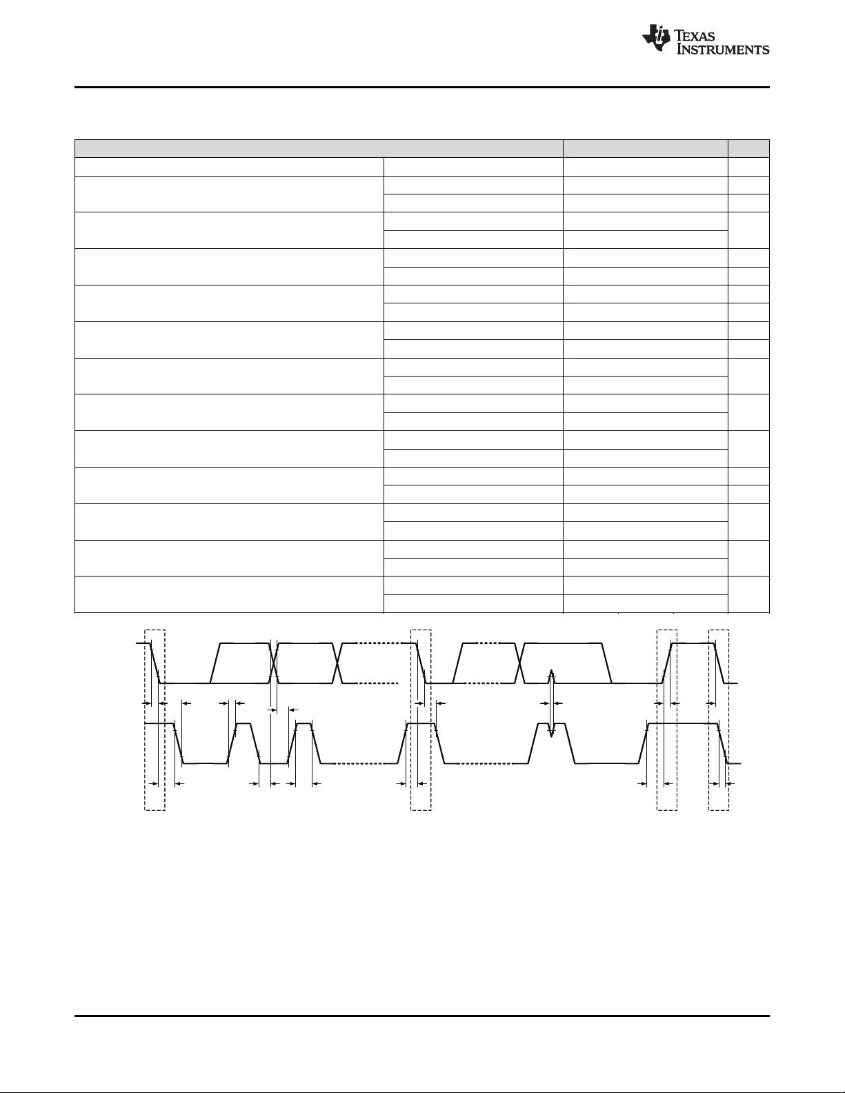
7.6 Timing Requirements: Data Transmission
V
= 3.6 V ±5%, TA= 25ºC, CL= 100 pF (unless otherwise noted)
BAT
f
(SCL)
t
HD;STA
t
LOW
t
HIGH
t
SU;STA
t
HD;DAT
t
SU;DAT
t
r
t
f
t
SU;STO
t
BUF
t
SP
C
b
Serial clock frequency 100 400 kHz
Hold time (repeated) START condition. After this
period, the first clock pulse is generated.
LOW period of the SCL clock µs
HIGH period of the SCL clock
Setup time for a repeated START condition
Data hold time
Data setup time ns
Rise time of both SDA and SCL signals ns
Fall time of both SDA and SCL signals ns
Setup time for STOP condition
Bus Free Time Between Stop and Start Condition µs
Pulse width of spikes that must be suppressed by
the input filter
Capacitive load for each bus line pF
SCL = 100 kHz 4 µs
SCL = 400 kHz 600 ns
SCL = 100 kHz 4.7
SCL = 400 kHz 1.3
SCL = 100 kHz 4 µs
SCL = 400 kHz 600 ns
SCL = 100 kHz 4.7 µs
SCL = 400 kHz 600 ns
SCL = 100 kHz 0 3.45 µs
SCL = 400 kHz 0 900 ns
SCL = 100 kHz 250
SCL = 400 kHz 100
SCL = 100 kHz 1000
SCL = 400 kHz 300
SCL = 100 kHz 300
SCL = 400 kHz 300
SCL = 100 kHz 4 µs
SCL = 400 kHz 600 ns
SCL = 100 kHz 4.7
SCL = 400 kHz 1.3
SCL = 100 kHz n/a n/a
SCL = 400 kHz 0 50
SCL = 100 kHz 400
SCL = 400 kHz 400
www.ti.com
MIN NOM MAX UNIT
ns
Figure 1. I2C Data Transmission Timing
10 Submit Documentation Feedback Copyright © 2011–2015, Texas Instruments Incorporated
Product Folder Links: TPS65186
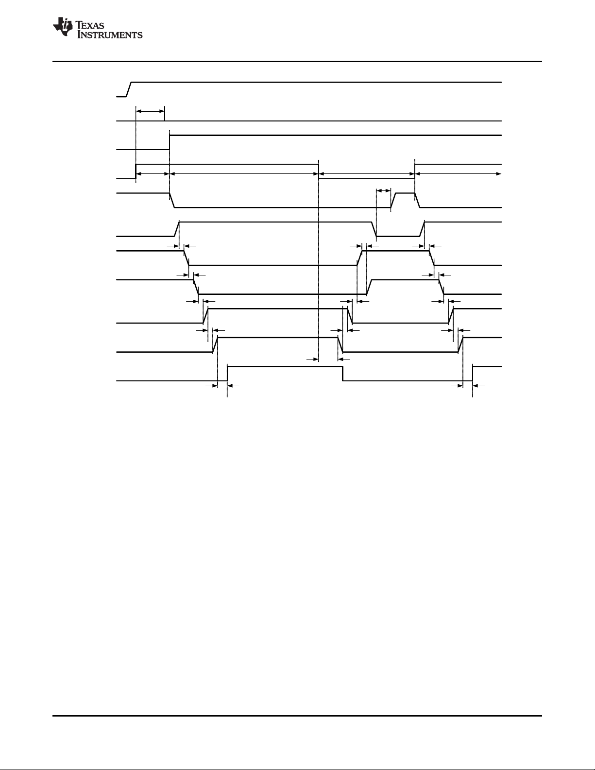
VIN
PWRUP
WAKEUP
VNEG
VEE
VPOS
VDDH
PWR _GOOD
VN
VB
1.8ms
DDLY2
DDLY3
DDLY4
DDLY1
300us max)(
STANDBY ACTIVE
SLEEP
ACTIVE
UDLY2
UDLY3
UDLY1
UDLY4
I2C
300us max)(
UDLY2
UDLY1
UDLY4
UDLY3
50ms
www.ti.com
TPS65186
SLVSB04A –JULY 2011–REVISED AUGUST 2015
Minimum delay time between WAKEUP rising edge and IC ready to accept I2C transaction.
In this example, the first power-up sequence is started by pulling the PWRUP pin high (rising edge). Power-down is
initiated by pulling the WAKEUP pin low (device enters sleep mode). The second power-up sequence is initiated by
pulling the WAKEUP pin high while the PWRUP pin is also high (power up from sleep to active).
Figure 2. Power-Up and Power-Down Timing Diagram
Copyright © 2011–2015, Texas Instruments Incorporated Submit Documentation Feedback 11
Product Folder Links: TPS65186
TPS65186
SLVSB04A –JULY 2011–REVISED AUGUST 2015
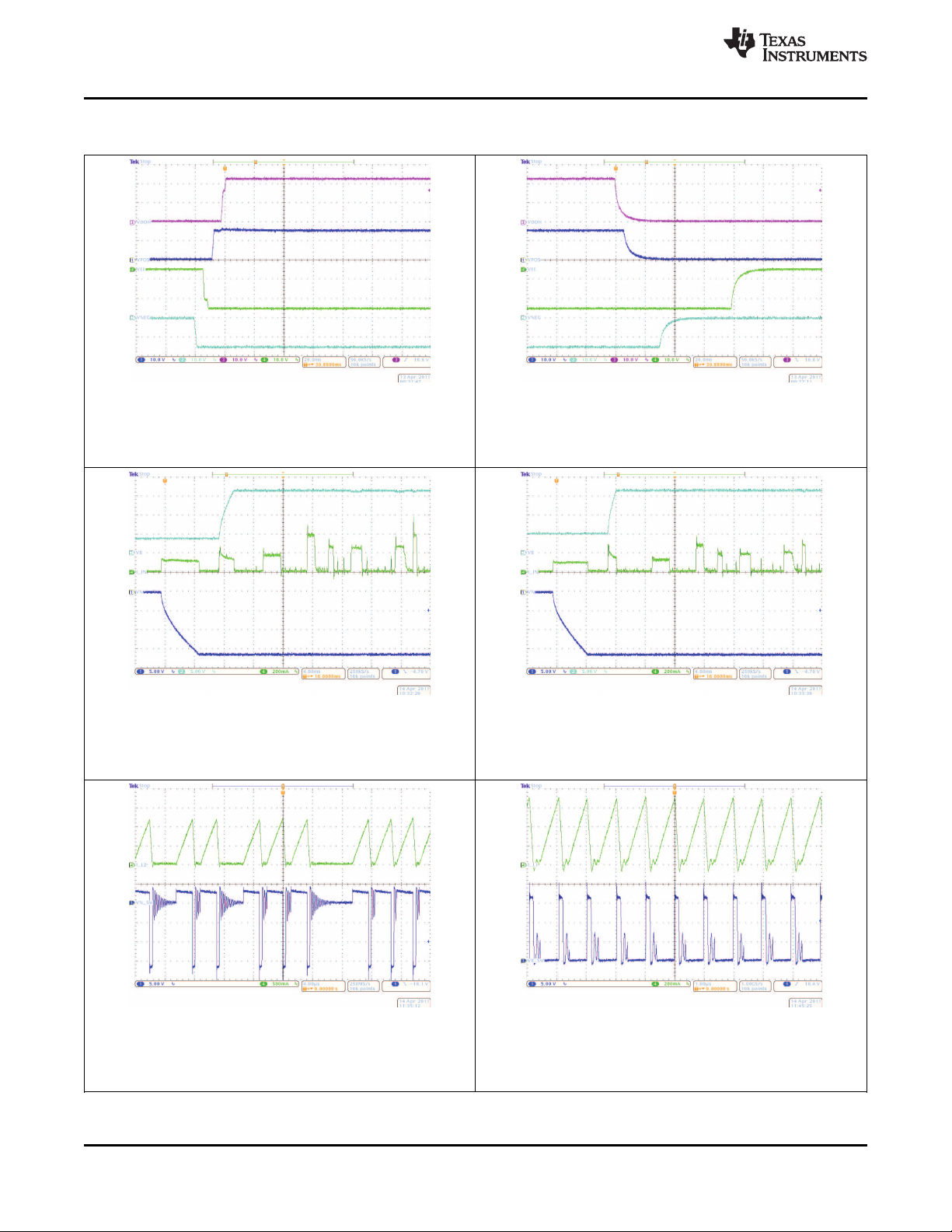
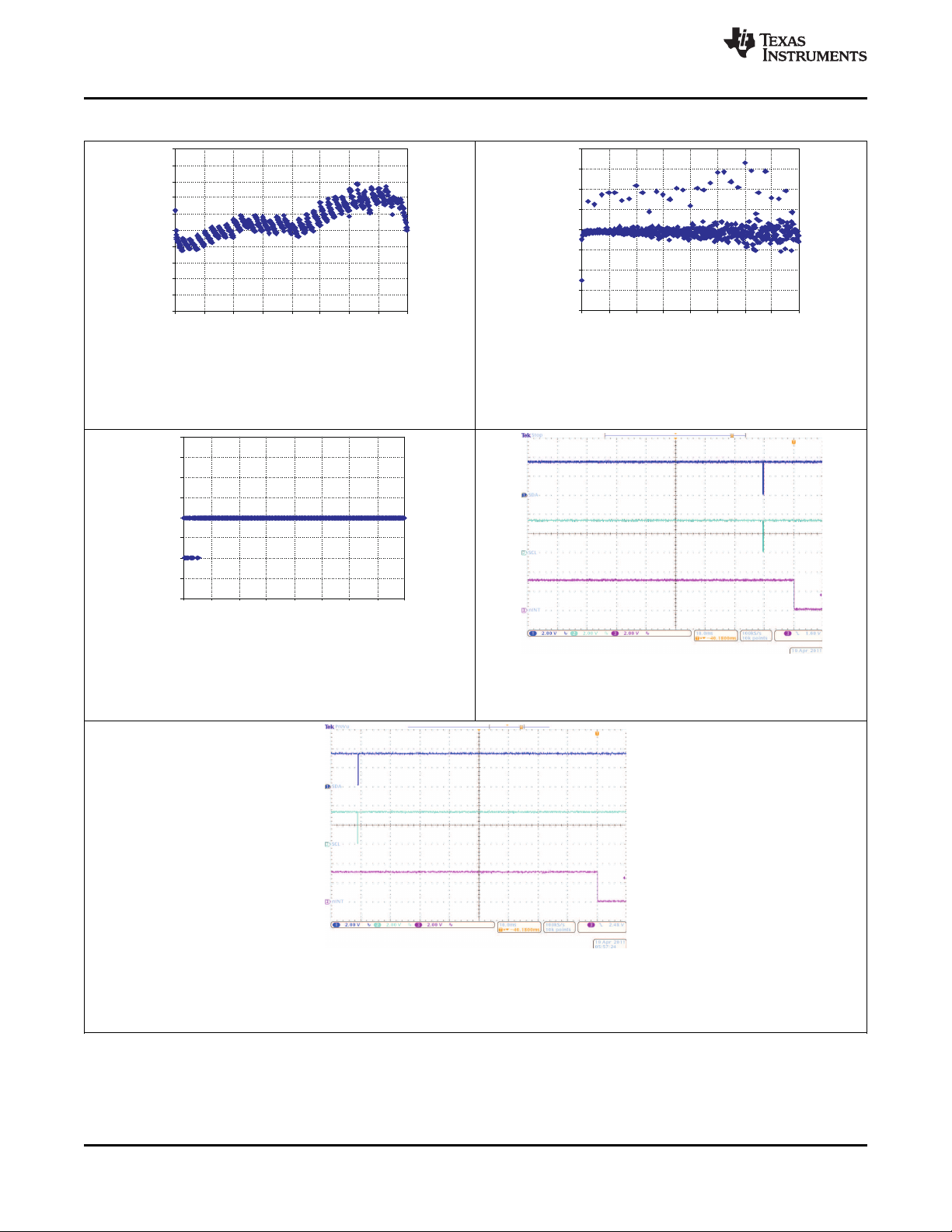
7.7 Typical Characteristics
Figure 3. Default Power-Up Sequence Figure 4. Default Power-Down Sequence
www.ti.com
VIN= 3.7 V CIN= 100 µF VIN= 5 V CIN= 100 µF
Figure 5. Inrush Current Figure 6. Inrush Current
VIN= 3 V R
LOAD, VPOS
= 330 Ω R
LOAD, VNEG
= 330 Ω VIN= 3 V R
LOAD, VPOS
= 330 Ω R
No Load on VDDH, VEE No Load on VDDH, VEE
Figure 7. Switching Waveforms, VN Figure 8. Switching Waveforms, VB
LOAD, VNEG
= 330 Ω
12 Submit Documentation Feedback Copyright © 2011–2015, Texas Instruments Incorporated
Product Folder Links: TPS65186
-5 0
-4 0
-3 0
-2 0
-1 0
0
1 0
2 0
3 0
4 0
5 0
0 25 50 75 100 12 5 1 50 1 75
C urr e nt [ m A]
VPOS + VNEG[mV]
IPO S= INEG
IPO S s we ep, INE G= 15m A
IPO S= 15m A, IN EG s wee p
0
5
10
15
20
25
1 1.5 2 2.5 3 3.5 4
VIN3P3[V]
R[ ], (VIN3p3-V3P3)/10mAW
www.ti.com
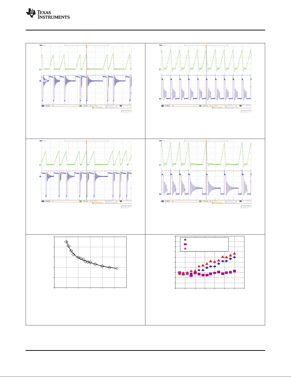
Typical Characteristics (continued)
TPS65186
SLVSB04A –JULY 2011–REVISED AUGUST 2015
VIN= 3.7 V R
No Load on VDDH, VEE No Load on VDDH, VEE
Figure 9. Switching Waveforms, VN Figure 10. Switching Waveforms, VB
VIN= 5 V R
No Load on VDDH, VEE No Load on VDDH, VEE
Figure 11. Switching Waveforms, VN Figure 12. Switching Waveforms, VB
LOAD, VPOS
LOAD, VPOS
= 330 Ω R
= 330 Ω R
LOAD, VNEG
LOAD, VNEG
= 330 Ω VIN= 3.7 V R
= 330 Ω VIN= 5 V R
LOAD, VPOS
LOAD, VPOS
= 330 Ω R
= 330 Ω R
LOAD, VNEG
LOAD, VNEG
= 330 Ω
= 330 Ω
VIN= 3.7 V I
Copyright © 2011–2015, Texas Instruments Incorporated Submit Documentation Feedback 13
Figure 13. 3p3V Switch Impedance
LOAD, V3p3
= 10 mA
VIN= 3.7 V
Figure 14. Source Driver Supply Tracking
Product Folder Links: TPS65186
-2
-1. 5
-1
-0. 5
0
0. 5
1
1. 5
2
0 640 12 80 192 0 25 60 3200 3840 44 80 512 0
Fo rce d Ki ckba c k V ol tag e [m V]
Measurement error [LSB]
-5
-4
-3
-2
-1
0
1
2
3
4
5
0 64 128 192 25 6 320 38 4 44 8 51 2
VC OM CO DE
INL[mV]
-0. 2
-0 .15
-0. 1
-0 .05
0
0 .05
0. 1
0 .15
0. 2
0 6 4 12 8 1 92 2 56 3 20 38 4 4 48 51 2
V COM CO DE
DNL[LSB]
TPS65186
SLVSB04A –JULY 2011–REVISED AUGUST 2015
Typical Characteristics (continued)
www.ti.com
VIN= 3.7 V R
LOAD, VCOM
= 1 kΩ VIN= 3.7 V R
LOAD, VCOM
= 1 kΩ
Figure 15. VCOM Integrated Non-Linearity Figure 16. VCOM Differential Non-Linearity
VIN= 3.7 V
VIN= 3.7 V AVG[1:0] = 00 (Single Measurement)
Time from ACQ Bit Set to ACQC Interrupt Received
Figure 17. Kickback Voltage Measurement Error
Figure 18. Kickback Voltage Measurement Timing
14 Submit Documentation Feedback Copyright © 2011–2015, Texas Instruments Incorporated
VIN= 3.7 V AVG[1:0] = 11 (Eight Measurements)
Time from ACQ Bit Set to ACQC Interrupt Received
Figure 19. Kickback Voltage Measurement Timing
Product Folder Links: TPS65186

TPS65186
www.ti.com
SLVSB04A –JULY 2011–REVISED AUGUST 2015
8 Detailed Description
8.1 Overview
The TPS65186 device provides two adjustable LDOs, inverting buck-boost converter, boost converter, thermistor
monitoring, and flexible power-up and power-down sequencing. The system can be supplied by a regulated input
voltage ranging from 3 V to 6 V. The device is characterized across a –10°C to 85°C temperature range, best
suited for personal electronic applications.
The I2C interface provides comprehensive features for using the TPS65186. All rails can be enabled or disabled.
Power-up and power-down sequences can also be programmed through the I2C interface, as well as thermistor
configuration and interrupt configuration. Voltage adjustment can also be controlled by the I2C interface.
The adjustable LDOs can supply up to 120 mA of current. The default output voltages for each LDO can be
adjusted through the I2C interface. LDO1 (VPOS) and LDO2 (VNEG) track each other in a way that they are of
opposite sign but same magnitude. The sum of VLDO1 and VLOD2 is guaranteed to be less than 50 mV.
There are two charge pumps: VDDH and VEE 10 mA and 12 mA respectively. These charge pumps boost the
DC-DC boost converters ±16-V rails to provide a gate channel supply.
The power good functionality is open-drain output, if any of the four power rails (CP1, CP2, LDO1, LDO2) are not
in regulation, encounters a fault, or is disabled the pin is pulled low. PWR_GOOD remains low if one of the rails
is not enabled by the host and only after all rails are in regulation PWR_GOOD is released to Hi-Z state (pulled
up by external resistor).
The TPS65186 provides circuitry to bias and measure an external NTC to monitor the display panel temperature
in a range from –10°C to 85°C with and accuracy of ±1°C from 0°C to 50°C. Temperature measurement are
triggered by the controlling host and the last temperature reading is always stored in the TMST_VALUE register.
Interrupts are issued when the temperature exceeds the programmable HOT, or drops below the programmable
COLD threshold, or when the temperature has changed by more than a user-defined threshold from the baseline
value.
This device is offered in a 48-Pin, 0.5-mm Pitch, 7 mm × 7 mm × 0.9 mm (VQFN) RGZ package.
Copyright © 2011–2015, Texas Instruments Incorporated Submit Documentation Feedback 15
Product Folder Links: TPS65186
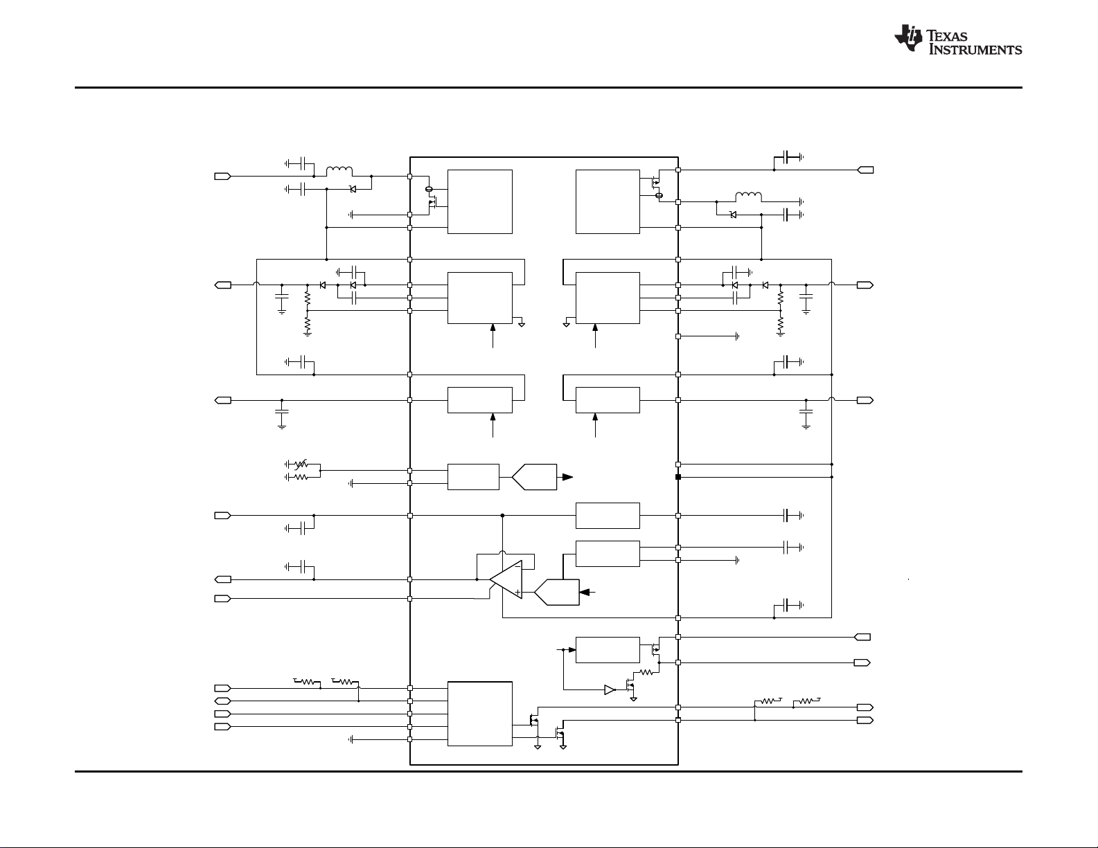
DCDC2
VIN_P
10uF
4.7uF
VPOS
10nF 2.2uF
1M
52.3k
VEE_D
VEE_DRV
VEE_FB
4.7uH
VN_SW
From Battery
(3.0V-6. 0V)
VEE (-20V)
VPOS (15V )
DCDC1
4.7uF
2.2uH
PGND1
VB_SW
10uF
10nF2.2uF
1M
47.5k
VDDH_D
VDDH_DRV
VDDH_FB
From Battery
(3.0V-6.0V )
VDDH (22 V)
VDDH_EN VEE_EN
PGND2 PGND2
VPOS_EN
VB
LDO1
VEE
CHARGE
PUMP
VN
PBKG
PGND2
4.7uF
VNEG_IN
VDDH_IN
VNEG
VNEG (-15V )
VNEG_EN
LDO2
PowerPad®
TEMP
SENSOR
43k
10k NTC
TS
AGND2 ADC
TMST_VALUE[7:0]
4.7uF
4.7uF
VPOS_IN
VIN
10uF
VCOM_PWR
4.7uF
From Input Supply
(3.0V-6. 0V)
4.7uF
VREF
AGND1
DAC
VCOM
VCOM[8:0]
VCOM_CTRL
4.7uF
From uC
VREF
4.7uF
INT_LDO
INT_LDO
VEE_IN
VDDH
CHARGE
PUMP
4.7uF
3.3V supply from system
To EPD panel
VIN3P3
V3P3
GATE DRIVER
V3P3_EN
1k
SCL
From uC
From/to uC or DSP
SDA
10k
VIO
PWR_GOOD
10k
VIO
DIGITAL
CORE
WAKEUP
INT
10k
VIO
10k
VIO
From uC
PWRUP
From uC
To uC
To uC
DGND
100n 100n
To panel back- plane
(0 to -5.11 V)
TPS65186
SLVSB04A –JULY 2011–REVISED AUGUST 2015
8.2 Functional Block Diagram
www.ti.com
16 Submit Documentation Feedback Copyright © 2011–2015, Texas Instruments Incorporated
Product Folder Links: TPS65186

TPS65186
www.ti.com
SLVSB04A –JULY 2011–REVISED AUGUST 2015
8.3 Feature Description
8.3.1 Wake-Up and Power-Up Sequencing
The power-up and power-down order and timing is defined by user register settings. The default settings support
the E Ink Vizplex panel and typically do not need to be changed.
In SLEEP mode the TPS65186 is completely turned off, the I2C registers are reset, and the device does not
accept any I2C transaction. Pull the WAKEUP pin high with the PWRUP pin low and the device enters STANDBY
mode that enables the I2C interface. Write to the UPSEQ0 register to define the order in which the output rails
are enabled at power-up and to the UPSEQ1 registers to define the power-up delays between rails. Finally, set
the ACTIVE bit in the ENABLE register to 1 to execute the power-up sequence and bring up all power rails.
Alternatively, pull the PWRUP pin high (rising edge).
After the ACTIVE bit has been set, the negative boost converter (VN) is powered up first, followed by the positive
boost (VB). The positive boost enable is gated by the internal power-good signal of the negative boost. Once VB
is in regulation, it issues an internal power-good signal and after delay time UDLY1 has expired, STROBE1 is
issued. The rail assigned to STROBE1 will power up next and after its power-good signal has been asserted and
delay time UDLY2 has expired, STROBE2 is issued. The sequence continues until STROBE4 has occurred and
the last rail has been enabled.
To power down the device, set the STANDBY bit of the ENABLE register to 1 or pull the PWRUP pin low (falling
edge) and the TPS65186 will power down in the order defined by DWNSEQx registers. The delay times DDLY2,
DDLY3, and DDLY4 are weighted by a factor of DFCTR which allows the user to space out the power down of
the rails to avoid crossing during discharge. DFCTR is located in register DWNSEQ1. The positive boost (VB) is
shut down together with the last rail at STROBE4. However, the negative boost (VN) remains up and running for
another 50 ms. Then VN is powered down and the device enters STANDBY or SLEEP mode, depending on the
WAKEUP pin.
If either the ACTIVE bit is set or the PWRUP pin is pulled high while the device is powering down, the powerdown sequence (STROBE1-4) is completed first, followed by a power-up sequence. VB and VN may or may not
be powered down and depending on the relative timing of STROBE4 to the new power-up event.
During power-up, if the STANDBY bit is set or the PWRUP pin is pulled low, the power-up sequence is aborted
and the power-down sequence starts immediately.
8.3.2 Dependencies Between Rails
Charge pumps, LDOs, and VCOM driver are dependent on the positive and inverting buck-boost converters and
several dependencies exist that affect the power-up sequencing. These dependencies are the following:
• Inverting buck-boost (DCDC2) must be in regulation before positive boost (DCDC1) can be enabled.
Internally, DCDC1 enable is gated by DCDC2 power good.
• Positive boost (DCDC1) must be in regulation before LDO2 (VNEG) can be enabled. Internally LDO2 enable
is gated DCDC1 power good.
• Positive boost (DCDC1) must be in regulation before VCOM can be enabled. Internally VCOM enable is
gated by DCDC1 power good.
• Positive boost (DCDC1) must be in regulation before negative charge pump (CP2) can be enabled. Internally
CP2 enable is gated by DCDC1 power good.
• Positive boost (DCDC1) must be in regulation before positive charge pump (CP1) can be enabled. Internally
CP1 enable is gated by DCDC1 power good.
• LDO2 must be in regulation before LDO1 can be enabled. Internally LDO1 enable is gated by LDO2 power
good.
Copyright © 2011–2015, Texas Instruments Incorporated Submit Documentation Feedback 17
Product Folder Links: TPS65186
 Loading...