

I/O
Control
From Input
Supply
(3 V to 6 V)
DCDC1
From Input
Supply
(3 V to 6 V)
VPOS
LDO1
VEE_D
VEE_DRV
VEE_FB
Negative
Charge
Pump
VCOM
VCOM
VCOM_PANEL
VNEG
VCOM
Temperature
Sensor
VIN
VB
VB_SW
TS
DCDC2
VN
VN_SW
VDDH_D
VDDH_DRV
VDDH_FB
Positive
Charge
Pump
LDO2
VIN3P3
Load Switch
V3P3
Copyright © 2017, Texas Instruments Incorporated
Product
Folder
Order
Now
Technical
Documents
Tools &
Software
Support &
Community
TPS65185, TPS651851
SLVSAQ8G –FEBRUARY 2011–REVISED SEPTEMBER 2017
TPS65185x PMIC for E Ink® Vizplex™ Enabled Electronic Paper Display
1 Features
1
• Single Chip Power-Management Solution for
E Ink®Vizplex™ Electronic Paper (E-Paper)
Displays
• Generates Positive and Negative Gates, and
Source Driver Voltages and Back-Plane Bias
From a Single, Low-Voltage Input Supply
• Supports 9.7-Inch and Larger Panel Sizes
• 3-V to 6-V Input Voltage Range
• Boost Converter for Positive Rail Base
• Inverting Buck-Boost Converter for Negative Rail
Base
• Two Adjustable LDOs for Source Driver Supply
– TPS65185 LDO1: 15 V, 120 mA (VPOS)
– TPS65185 LDO2: –15 V, 120 mA (VNEG)
– TPS651851 LDO1: 15 V, 200 mA at
VIN≥ 3.6 V (VPOS)
– TPS651851 LDO2: –15 V, 200 mA at
VIN≥ 3.6 V (VNEG)
• Accurate Output Voltage Tracking
– VPOS – VNEG = ±50 mV
• Two Charge Pumps for Gate Driver Supply
– CP1: 22 V, 15 mA (VDDH)
– CP2: –20 V, 15 mA, (VEE)
• Adjustable VCOM Driver for Accurate PanelBackplane Biasing
– 0 V to –5.11 V
– ± 1.5% accuracy (±10 mV)
– 9-Bit Control (10-mV Nominal Step Size)
• Active Discharge on All Rails
• Integrated 10-Ω, 3.3-V Power Switch for Disabling
System Power Rail to E-Ink Panel
2 Applications
• Power Supply for Active Matrix E Ink Vizplex
Panels
• Electronic Paper Display (EPD) Power Supplies
• E-Book Readers
• Dual-Display Phone and Tablets
• Application Processors With Integrated or
Software Timing Controller (OMAP™)
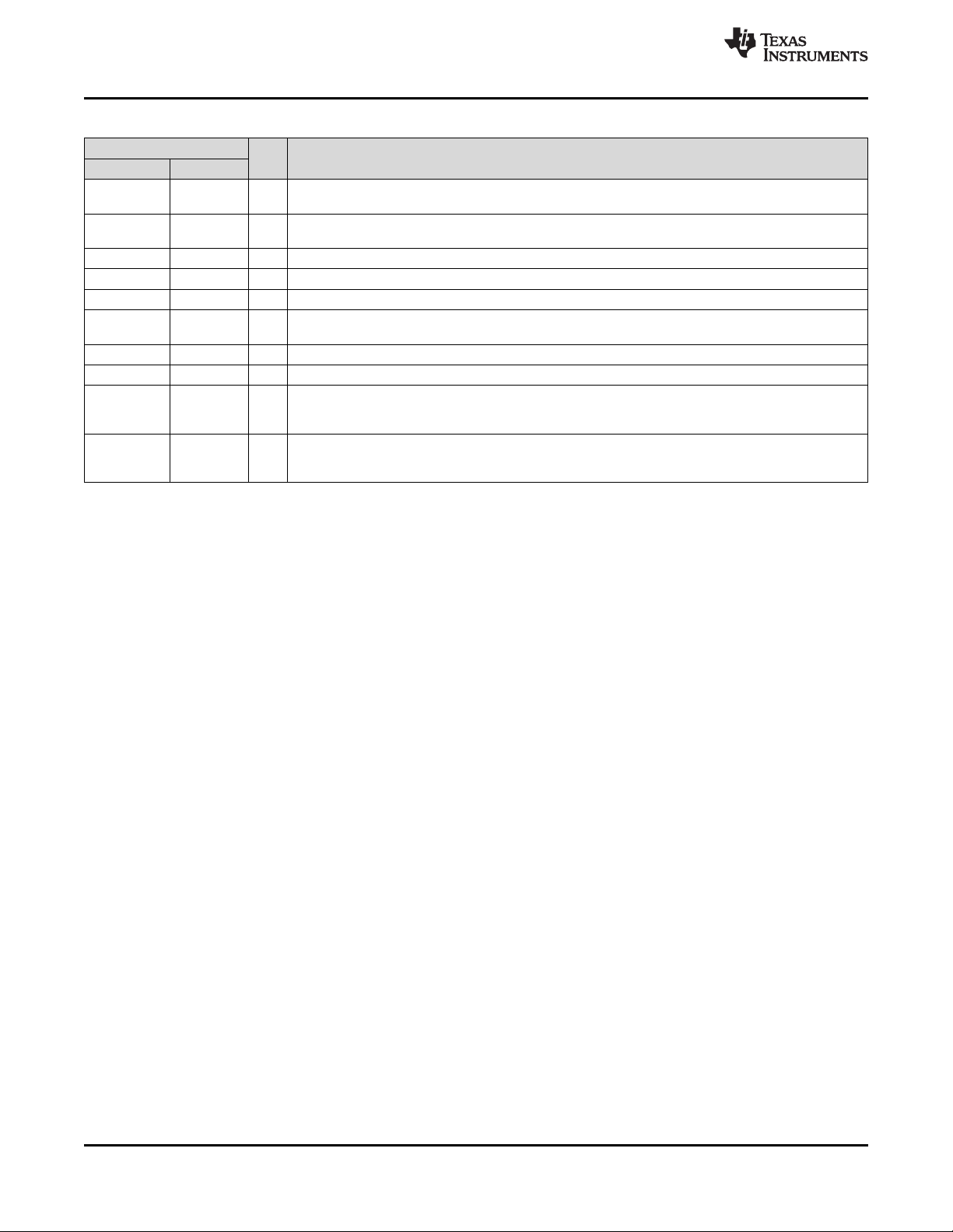
3 Description
The TPS65185x device is a single-chip power supply
designed to for E Ink Vizplex displays used in
portable e-reader applications, and the device
supports panel sizes up to 9.7 inches and greater.
Two high efficiency DC-DC boost converters
generate ±16-V rails that are boosted to 22 V and
–20 V by two change pumps to provide the gate
driver supply for the Vizplex panel. Two tracking
LDOs create the ±15-V source driver supplies that
support up to 120/200 mA (TPS65185/TPS651851) of
output current. All rails are adjustable through the I2C
interface to accommodate specific panel
requirements.
Device Information
PART NUMBER PACKAGE BODY SIZE (NOM)
TPS65185
TPS651851 RSL (48) 6.00 mm × 6.00 mm
(1) For all available packages, see the orderable addendum at
the end of the data sheet.
RGZ (48) 7.00 mm × 7.00 mm
RSL (48) 6.00 mm × 6.00 mm
(1)
Typical Application Schematic
1
An IMPORTANT NOTICE at the end of this data sheet addresses availability, warranty, changes, use in safety-critical applications,
intellectual property matters and other important disclaimers. PRODUCTION DATA.

TPS65185, TPS651851
SLVSAQ8G –FEBRUARY 2011–REVISED SEPTEMBER 2017
www.ti.com
Table of Contents
1 Features.................................................................. 1
2 Applications ........................................................... 1
3 Description ............................................................. 1
4 Revision History..................................................... 2
5 Description (continued)......................................... 4
6 Pin Configuration and Functions......................... 4
7 Specifications......................................................... 7
7.1 Absolute Maximum Ratings ...................................... 7
7.2 ESD Ratings.............................................................. 7
7.3 Recommended Operating Conditions....................... 7
7.4 Thermal Information.................................................. 8
7.5 Electrical Characteristics........................................... 8
7.6 Timing Requirements: Data Transmission.............. 12
7.7 Typical Characteristics............................................ 14
8 Detailed Description............................................ 17
8.1 Overview ................................................................. 17
8.2 Functional Block Diagram....................................... 18
8.3 Feature Description................................................. 19
8.4 Device Functional Modes........................................ 27
8.5 Programming........................................................... 29
8.6 Register Maps......................................................... 31
9 Application and Implementation ........................ 49
9.1 Application Information............................................ 49
9.2 Typical Application.................................................. 49
10 Power Supply Recommendations ..................... 51
11 Layout................................................................... 52
11.1 Layout Guidelines ................................................. 52
11.2 Layout Example .................................................... 52
12 Device and Documentation Support................. 53
12.1 Device Support...................................................... 53
12.2 Documentation Support ........................................ 53
12.3 Receiving Notification of Documentation Updates 53
12.4 Community Resources.......................................... 53
12.5 Trademarks........................................................... 53
12.6 Electrostatic Discharge Caution............................ 53
12.7 Glossary................................................................ 53
13 Mechanical, Packaging, and Orderable
Information........................................................... 53
4 Revision History
NOTE: Page numbers for previous revisions may differ from page numbers in the current version.
Changes from Revision F (June 2017) to Revision G Page
• Added the load switch and updated the negative and positive charge pumps in the Typical Application Schematic figure . 1
• Added capacitor connection to the pin description for INT_LDO, VB, VCOM, VCOM_PWR, VDDH_D, VEE_D, VIN,
VIN_P, VN, VNEG, VNEG_IN, VPOS, VPOS_IN, VREF in the Pin Functions table............................................................. 5
• Changed the Power-Up and Power-Down Timing Diagram ................................................................................................ 13
• Changed the Functional Block Diagram............................................................................................................................... 18
• Changed the schematic in the Typical Application section.................................................................................................. 49
Changes from Revision E (February 2017) to Revision F Page
• Updated pin out drawing to match Pin Functions table.......................................................................................................... 4
Changes from Revision D (December 2016) to Revision E Page
• Changed changed the maximum input voltage for TPS651851 from 5.9 V to 6 V................................................................ 7
• Changed the VINrange to the V
OUTTOL
and V
parameters in the Electrical Characteristics table..................................... 9
DIFF
• Changed the Electrostatic Discharge Caution statement..................................................................................................... 53
Changes from Revision C (August 2015) to Revision D Page
• Added TPS651851 device to the data sheet.......................................................................................................................... 1
• Added the input voltage range for TPS651851 ...................................................................................................................... 1
• Added TPS651851 LDO1 and LDO2 current limit of 200 mA................................................................................................ 1
• Updated the switch current limit to 2.5 A on DCDC1 for TPS651851 ................................................................................... 8
• Updated the LDO1 ILOAD current limit for TPS651851 ........................................................................................................ 9
• Updated the LDO1 ILIMIT current limit for TPS651851 ........................................................................................................ 9
2
Submit Documentation Feedback Copyright © 2011–2017, Texas Instruments Incorporated
Product Folder Links: TPS65185
TPS65185, TPS651851
www.ti.com
• Updated the LDO2 ILOAD current range for different VIN conditions .................................................................................. 9
• Updated the LDO2 ILIMIT output current limit to different VIN conditions............................................................................. 9
• Updated the output voltage range (VDDH_OUT) conditions on charge pump 1 ................................................................ 10
• Added the ILOAD current range option for TPS651851 on CP1 ........................................................................................ 10
• Added the ILOAD current range option for TPS651851 on CP2 ........................................................................................ 10
• Added Receiving Notification of Documentation Updates to Device and Documentation Support section ......................... 53
Changes from Revision B (October 2011) to Revision C Page
• Added ESD Ratings table, Feature Description section, Device Functional Modes, Application and Implementation
section, Power Supply Recommendations section, Layout section, Device and Documentation Support section, and
Mechanical, Packaging, and Orderable Information section.................................................................................................. 1
SLVSAQ8G –FEBRUARY 2011–REVISED SEPTEMBER 2017
Product Folder Links: TPS65185
Submit Documentation FeedbackCopyright © 2011–2017, Texas Instruments Incorporated
3
36 VDDH_DRV1VREF
37VDDH_IN 24 VIN_P
35 VDDH_DIS2INT
38N/C 23 PWR_GOOD
34 VDDH_D3VNEG
39N/C 22 PBKG
33 VDDH_FB4VNEG_IN
40VB_SW 21 PWRUP
32 PGND25WAKEUP
41PGND1 20 N/C
31 VEE_FB6DGND
42VB 19 VPOS_DIS
30 VEE_D7INT_LDO
43VPOS_IN 18 SDA
29 VEE_DIS8AGND1
44VPOS 17 SCL
28 VEE_DRV9VNEG_DIS
45VIN3P3 16 VCOM_PWR
27 VEE_IN10VIN
46V3P3 15 VCOM
26 VN11N/C
47TS 14 VCOM_DIS
25 VN_SW12VCOM_CTRL
48AGND2 13 N/C
Not to scale
Thermal
Pad
TPS65185, TPS651851
SLVSAQ8G –FEBRUARY 2011–REVISED SEPTEMBER 2017
www.ti.com
5 Description (continued)
Accurate back-plane biasing is provided by a linear amplifier that can be adjusted from 0 V to –5.11 V with 9-bit
control through the serial interface; it can source or sink current depending on panel condition. The TPS65185x
supports automatic panel kickback voltage measurement, which eliminates the need for manual VCOM
calibration in the production line. The measurement result can be stored in non-volatile memory to become the
new VCOM power-up default value.
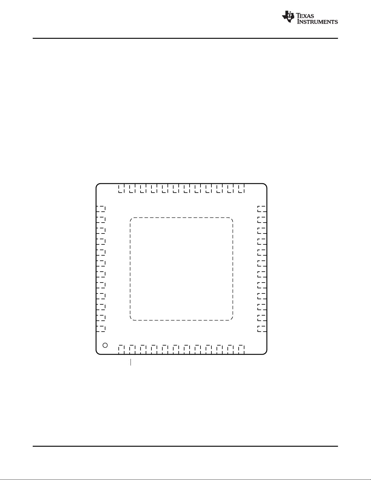
TPS65185 is available in two packages, a 48-pin 7-mm × 7-mm2VQFN (RGZ) with 0.5-mm pitch, and a 48-pin
6-mm × 6-mm2VQFN (RSL) with 0.4-mm pitch. The TPS651851 is available in a 48-pin 6-mm × 6-mm2VQFN
(RSL) with 0.4-mm pitch.
6 Pin Configuration and Functions
RGZ Package and RSL Package
48-Pin VQFN With Exposed Thermal Pad
Top View
4
Submit Documentation Feedback Copyright © 2011–2017, Texas Instruments Incorporated
Product Folder Links: TPS65185
TPS65185, TPS651851
www.ti.com
SLVSAQ8G –FEBRUARY 2011–REVISED SEPTEMBER 2017
Pin Functions
PIN
NAME NO.
AGND1 8 — Analog ground for general analog circuitry.
AGND2 48 — Reference point to external thermistor and linearization resistor.
DGND 6 — Digital ground. Connect to ground plane.
INT 2 O Open drain interrupt pin (active low).
INT_LDO 7 O Filter pin for 2.7-V internal supply. Connect a 4.7-µF capacitor from this pin to ground.
N/C
11, 13, 20,
38, 39
PBKG 22 —
PGND1 41 — Power ground for DCDC1.
PGND2 32 — Power ground for CP1 (VDDH) and CP2 (VEE) charge pumps.
PWR_GOOD 23 O
PWRUP 21 I Power-up pin. Pull this pin high to power up all output rails.
SCL 17 I Serial interface (I2C) clock input.
SDA 18 I/O Serial interface (I2C) data input/output.
TS 47 I
V3P3 46 O Output pin of 3.3-V power switch.
VB 42 I
VB_SW 40 O Boost converter switch out (DCDC1).
VCOM 15 O Filter pin for panel common-voltage driver. Connect a 4.7-µF capacitor from this pin to ground.
VCOM_CTRL 12 I
VCOM_DIS 14 I
VCOM_PWR 16 I
VDDH_D 34 O
VDDH_DIS 35 I
VDDH_DRV 36 O Driver output pin for positive charge pump (CP1).
VDDH_FB 33 I Feedback pin for positive charge pump (CP1).
VDDH_IN 37 I Input supply pin for positive charge pump (CP1).
VEE_D 30 O
VEE_DIS 29 I
VEE_DRV 28 O Driver output pin for negative charge pump (CP2).
VEE_FB 31 I Feedback pin for negative charge pump (CP2).
VEE_IN 27 I Input supply pin for negative charge pump (CP2) (VEE).
VIN 10 I Input power supply to general circuitry. Connect a 10-µF capacitor from this pin to ground.
VIN3P3 45 I Input pin to 3.3-V power switch.
VIN_P 24 I
VN 26 I
I/O DESCRIPTION
— Not internally connected.
Die substrate. Connect to the VN pin (–16 V) with a short, wide trace. A wide copper trace improves
heat dissipation.
Open-drain power good output pin. Pin is pulled low when one or more rails are disabled or not in
regulation. DCDC1, DCDC2, and VCOM have no effect on this pin.
(1)
(1)
Thermistor input pin. Connect a 10-kΩ NTC thermistor and a 43-kΩ linearization resistor between this
pin and AGND.
Feedback pin for boost converter (DCDC1) and supply for VPOS LDO and VDDH charge pump.
Connect a 4.7-µF capacitor from this pin to ground.
VCOM enable. Pull this pin high to enable the VCOM amplifier. When pin is pulled low and VN is
enabled, VCOM discharge is enabled.
(2)
Discharge pin for VCOM. Connect to ground to discharge VCOM to ground whenever VCOM is
disabled. Leave floating if discharge function is not desired.
Internal supply input pin to VCOM buffer. Connect to the output of DCDC2, and connect a 4.7-µF
capacitor from this pin to ground.
Base voltage output pin for positive charge pump (CP1). Connect a 100-nF capacitor from this pin to
ground.
Discharge pin for VDDH. Connect to VDDH to discharge VDDH to ground whenever the rail is
disabled. Leave floating if discharge function is not desired.
Base voltage output pin for negative charge pump (CP2). Connect a 100-nF capacitor from this pin to
ground.
Discharge pin for VEE. Connect a resistor from VEE _DIS to VEE to discharge VEE to ground
whenever the rail is disabled. Leave floating if discharge function is not desired.
Input power supply to inverting buck-boost converter (DCDC2). Connect a 10-µF capacitor from this
pin to ground.
Feedback pin for inverting buck-boost converter (DCDC2) and supply for VNEG LDO and VEE charge
pump. Connect a 4.7-µF capacitor from this pin to ground.
(1) There will be 0-ns of deglitch for PWRx.
(2) There will be 62.52-µs of deglitch for VCOM_CTRL.
Product Folder Links: TPS65185
Submit Documentation FeedbackCopyright © 2011–2017, Texas Instruments Incorporated
5
TPS65185, TPS651851
SLVSAQ8G –FEBRUARY 2011–REVISED SEPTEMBER 2017
www.ti.com
Pin Functions (continued)
PIN
NAME NO.
VNEG 3 O
VNEG_DIS 9 O
VNEG_IN 4 I Input pin for LDO2 (VNEG). Connect a 4.7-µF capacitor from this pin to ground.
VN_SW 25 O Inverting buck-boost converter switch out (DCDC2).
VPOS 44 O Positive supply output pin for panel source drivers. Connect a 4.7-µF capacitor from this pin to ground.
VPOS_DIS 19 I
VPOS_IN 43 I Input pin for LDO1 (VPOS). Connect a 4.7-µF capacitor from this pin to ground.
VREF 1 O Filter pin for 2.25-V internal reference to ADC. Connect a 4.7-µF capacitor from this pin to ground.
WAKEUP 5 I
Thermal Pad — —
(3) There will be 93.75-µs of deglitch for WAKEUP.
I/O DESCRIPTION
Negative supply output pin for panel source drivers. Connect a 4.7-µF capacitor from this pin to
ground.
Discharge pin for VNEG. Connect to VNEG to discharge VNEG to ground whenever the rail is
disabled. Leave floating if discharge function is not desired.
Discharge pin for VPOS. Connect a resistor from VPOS_DIS to VPOS to discharge VPOS to ground
whenever the rail is disabled. Leave floating if discharge function is not desired.
Wake up pin (active high). Pull this pin high to wake up from sleep mode. The device accepts I2C
commands after WAKEUP pin is pulled high but power rails remain disabled until PWRUP pin is pulled
(3)
high.
The thermal pad is internally connected to the PBKG pin. Connect the thermal pad to the VN pin with a
short, wide trace. A wide copper trace improves heat dissipation. Do not connect the thermal pad to
ground.
6
Submit Documentation Feedback Copyright © 2011–2017, Texas Instruments Incorporated
Product Folder Links: TPS65185
TPS65185, TPS651851
www.ti.com
SLVSAQ8G –FEBRUARY 2011–REVISED SEPTEMBER 2017
7 Specifications
7.1 Absolute Maximum Ratings
over operating free-air temperature range (unless otherwise noted)
Input voltage at VIN
Ground pins to system ground –0.3 0.3 V
Voltage at SDA, SCL, WAKEUP, PWRUP, VCOM_CTRL, VDDH_FB, VEE_FB, PWR_GOOD,
nINT
Voltage on VB, VB_SW, VPOS_IN, VPOS_DIS, VDDH_IN –0.3 20 V
VDDH_DIS –0.3 30 V
Voltage on VN, VEE_IN, VCOM_PWR, VNEG_DIS, VNEG_IN –20 0.3 V
Voltage from VIN_P to VN_SW –0.3 30 V
Voltage on VCOM_DIS –5 0.3 V
VEE_DIS –30 0.3 V
Peak output current Internally limited mA
Continuous total power dissipation 2 W
TJOperating junction temperature –10 125 °C
TAOperating ambient temperature
T
Storage temperature –65 150 °C
stg
(1) Stresses beyond those listed under Absolute Maximum Ratings may cause permanent damage to the device. These are stress ratings
only, and functional operation of the device at these or any other conditions beyond those indicated under Recommended Operating
Conditions is not implied. Exposure to absolute maximum rated conditions for extended periods may affect device reliability.
(2) All voltage values are with respect to network ground terminal.
(3) It is recommended that copper plane in proper size on board be in contact with die thermal pad to dissipate heat efficiently. Thermal pad
is electrically connected to PBKG, which is supposed to be tied to the output of buck-boost converter. Thus wide copper trace in the
buck-boost output will help heat dissipated efficiently.
(2)
, VIN_P, VIN3P3 –0.3 7 V
(3)
(1)(2)
MIN MAX UNIT
–0.3 3.6 V
–10 85 °C
7.2 ESD Ratings
V
(ESD)
Electrostatic discharge
Human-body model (HBM), per ANSI/ESDA/JEDEC JS-001
Charged-device model (CDM), per JEDEC specification JESD22-C101
(1) JEDEC document JEP155 states that 500-V HBM allows safe manufacturing with a standard ESD control process.
(2) JEDEC document JEP157 states that 250-V CDM allows safe manufacturing with a standard ESD control process.
(1)
(2)
7.3 Recommended Operating Conditions
over operating free-air temperature range (unless otherwise noted)
MIN NOM MAX UNIT
Input voltage at VIN, VIN_P, VIN3P3 3 3.7 6 V
Voltage at SDA, SCL, WAKEUP, PWRUP, VCOM_CTRL, VDDH_FB,
VEE_FB, PWR_GOOD, nINT
T
A
T
J
Operating ambient temperature –10 85 °C
Operating junction temperature –10 125 °C
0 3.6 V
VALUE UNIT
±2000
±500
V
Product Folder Links: TPS65185
Submit Documentation FeedbackCopyright © 2011–2017, Texas Instruments Incorporated
7
TPS65185, TPS651851
SLVSAQ8G –FEBRUARY 2011–REVISED SEPTEMBER 2017
www.ti.com
7.4 Thermal Information
TPS65185 TPS651851
THERMAL METRIC
(1)
UNITRGZ (VQFN) RSL (VQFN) RSL (VQFN)
48 PINS 48 PINS 48 PINS
R
θJA
R
θJC(top)
R
θJB
ψ
JT
ψ
JB
R
θJC(bot)
Junction-to-ambient thermal resistance 30 30 30 °C/W
Junction-to-case (top) thermal resistance 15.6 16.2 16.2 °C/W
Junction-to-board thermal resistance 6.6 5.1 5.1 °C/W
Junction-to-top characterization parameter 0.2 0.2 0.2 °C/W
Junction-to-board characterization parameter 6.6 5.1 5.1 °C/W
Junction-to-case (bottom) thermal resistance 0.9 0.9 0.9 °C/W
(1) For more information about traditional and new thermal metrics, see the Semiconductor and IC Package Thermal Metrics application
report.
7.5 Electrical Characteristics
PARAMETER TEST CONDITIONS MIN TYP MAX UNIT
INPUT VOLTAGE
V
IN
V
UVLO
V
HYS
INPUT CURRENT
I
Q
I
STD
I
SLEEP
INTERNAL SUPPLIES
VI
NT_LDO
C
INT_LDO
V
REF
C
REF
DCDC1 (POSITIVE BOOST REGULATOR)
V
IN
PG
V
OUT
I
OUT
R
DS(ON)
I
LIMIT
f
SW
L
DCDC1
C
DCDC1
ESR Output capacitor ESR 20 mΩ
DCDC2 (INVERTING BUCK-BOOST REGULATOR)
V
IN
PG
V
OUT
I
OUT
Input voltage range 3 3.7 6 V
Undervoltage lockout threshold VINfalling 2.9 V
Undervoltage lockout hysteresis VINrising 400 mV
Operating quiescent current into VINDevice switching, no load 5.5 mA
Operating quiescent current into VINDevice in standby mode 130 µA
Shutdown current Device in sleep mode 3.5 10 µA
Internal supply 2.7 V
Nominal output capacitor Capacitor tolerance ±10% 1 4.7 µF
Internal supply 2.25 V
Nominal output capacitor Capacitor tolerance ±10% 3.3 4.7 µF
Input voltage range 3 3.7 6 V
Power good threshold Fraction of nominal output voltage 90%
Power good time-out Not tested in production 50 ms
Output voltage range 16 V
DC set tolerance –4.5% 4.5%
Output current 250 mA
MOSFET on resistance VIN= 3.7 V 350 mΩ
Switch current limit (TPS65185) 1.5
Switch current limit (TPS651851) 2.5
Switch current accuracy –30% 30%
Switching frequency 1 MHz
Inductor 2.2 µH
Nominal output capacitor Capacitor tolerance ±10% 1 2 × 4.7 µF
Input voltage range 3 3.7 6 V
Power good threshold Fraction of nominal output voltage 90%
Power good time-out Not tested in production 50 ms
Output voltage range –16 V
DC set tolerance –4.5% 4.5%
Output current 250 mA
A
8
Submit Documentation Feedback Copyright © 2011–2017, Texas Instruments Incorporated
Product Folder Links: TPS65185
TPS65185, TPS651851
www.ti.com
SLVSAQ8G –FEBRUARY 2011–REVISED SEPTEMBER 2017
Electrical Characteristics (continued)
PARAMETER TEST CONDITIONS MIN TYP MAX UNIT
R
DS(ON)
I
LIMIT
L
DCDC1
C
DCDC1
ESR Capacitor ESR 20 mΩ
LDO1 (VPOS)
V
POS_IN
PG
V
SET
V
INTERVAL
V
OUTTOL
V
DROPOUT
V
LOADREG
I
LOAD
I
LIMIT
R
DIS
C
LDO1
LDO2 (VNEG)
V
NEG_IN
PG
V
SET
V
INTERVAL
V
OUTTOL
V
DROPOUT
V
LOADREG
I
LOAD
I
LIMIT
R
DIS
T
SS
C
LDO2
MOSFET on resistance VIN= 3.7 V 350 mΩ
Switch current limit 1.5 A
Switch current accuracy –30% 30%
Inductor 4.7 µH
Nominal output capacitor Capacitor tolerance ±10% 1 3 × 4.7 µF
Input voltage range 15.2 16 16.8 V
Power good threshold Fraction of nominal output voltage 90%
Power good time-out Not tested in production 50 ms
Output voltage set value
VIN= 16 V,
VSET[2:0] = 0x3h to 0x6h
14.25 15 V
Output voltage set resolution VIN= 16 V 250 mV
Output tolerance
Dropout voltage I
Load regulation – DC I
= 15 V, I
SET
5.9 V
= 120 mA 250 mV
LOAD
= 10% to 90% 1%
LOAD
= 20 mA, 3 V ≤ VIN<
LOAD
–1% 1%
V
Load current range (TPS65185) VIN≥ 3 V 120
Load current range (TPS651851)
3 V ≤ VIN< 3.6 V 150
VIN≥ 3.6 V 200
Output current limit (TPS65185) VIN≥ 3 V 120
Output current limit (TPS651851)
3 V ≤ VIN< 3.6 V 150
VIN≥ 3.6 V 200
Discharge impedance to ground Enabled when rail is disabled 800 1000 1200 Ω
Mismatch to any other RDIS –2% 2%
Nominal output capacitor Capacitor tolerance ±10% 1 4.7 µF
Input voltage range 15.2 16 16.8 V
Power good threshold Fraction of nominal output voltage 90%
Power good time-out Not tested in production 50 ms
Output voltage set value
VIN= –16 V
VSET[2:0] = 0x3h to 0x6h
–15 –14.25 V
Output voltage set resolution VIN= –16 V 250 mV
Output tolerance V
Dropout voltage I
Load regulation – DC I
Load current range
= –15 V, I
SET
= 120 mA 250 mV
LOAD
= 10% to 90% 1%
LOAD
= –20 mA –1% 1%
LOAD
3 V ≤ VIN< 3.6 V (TPS65185 and
TPS651851)
120
VIN≥ 3.6 V (TPS65185 and TPS651851) 200
3 V ≤ VIN< 3.6 V (TPS65185) 180
Output current limit
VIN≥ 3.6 V (TPS65185 and TPS651851) 200
Discharge impedance to ground Enabled when rail is disabled 800 1000 1200 Ω
Mismatch to any other RDIS –2% 2%
Soft-start time Not tested in production 1 ms
Nominal output capacitor Capacitor tolerance ±10% 1 4.7 µF
mA
mA
mA
mA3 V ≤ VIN< 3.6 V (TPS651851) 158
Product Folder Links: TPS65185
Submit Documentation FeedbackCopyright © 2011–2017, Texas Instruments Incorporated
9
TPS65185, TPS651851
SLVSAQ8G –FEBRUARY 2011–REVISED SEPTEMBER 2017
Electrical Characteristics (continued)
PARAMETER TEST CONDITIONS MIN TYP MAX UNIT
LD01 (POS) AND LDO2 (VNEG) TRACKING
V
DIFF
Difference between VPOS and VNEG
VCOM DRIVER
I
VCOM
Drive current 15 mA
Allowed operating range
Accuracy
V
COM
Output voltage range –5.11 0 V
Resolution 1LSB 10 mV
Max number of EEPROM writes V
R
R
C
IN
DIS
VCOM
Input impedance, HiZ state HiZ = 1 150 MΩ
Discharge impedance to ground VCOM_CTRL = low, Hi-Z = 0 800 1000 1200 Ω
Mismatch to any other R
DIS
Nominal output capacitor Capacitor tolerance ±10% 3.3 4.7 µF
CP1 (VDDH) CHARGE PUMP
V
DDH_IN
PG
V
FB
V
DDH_OUT
I
LOAD
f
SW
R
DIS
C
D
C
O
Input voltage range 15.2 16 16.8 V
Power good threshold Fraction of nominal output voltage 90%
Power good time-out Not tested in production 50 ms
Feedback voltage 0.998 V
Accuracy I
Output voltage range
Load current range (TPS65185) 10
Load current range (TPS651851) 15
Switching frequency 560 kHz
Discharge impedance to ground Enabled when rail is disabled 800 1000 1200 Ω
Mismatch to any other R
DIS
Driver capacitor 10 nF
Output capacitor 1 2.2 µF
CP2 (VEE) NEGATIVE CHARGE PUMP
V
EE_IN
PG
V
FB
V
EE_OUT
I
LOAD
f
SW
R
DIS
Input voltage range 15.2 16 16.8 V
Power good threshold Fraction of nominal output voltage 90%
Power good time-out Not tested in production 50 ms
Feedback voltage –0.994 V
Accuracy I
Output voltage range V
Load current range (TPS65185) 12
Load current range (TPS651851) 15
Switching frequency 560 kHz
Discharge impedance to ground Enabled when rail is disabled 800 1000 1200 Ω
Mismatch to any other R
DIS
V
I
V ≤ VIN< 5.9 V
Outside this range VCOM is shut down
and VCOMF interrupt is set
VCOM[8:0] = 0x07Dh
(–1.25 V), VIN= 3.4 V to 4.2 V, no load
VCOM[8:0] = 0x07Dh
(–1.25 V), VIN= 3 V to 6 V, no load
V
R10 = 47.5 kΩ
V
R10 = 41.6 kΩ
V
R10 = 37 kΩ
= ±15 V,
SET
= ±20 mA, 0°C to 60°C ambient, 3
LOAD
–50 50 mV
–5.5 1 V
–0.8% 0.8%
–1.5% 1.5%
calibration 100
COM
–2% 2%
= 2 mA –2% 2%
LOAD
SET
SET
SET
= 22 V, I
= 25 V, I
= 28 V, I
= 2 mA, R6 = 1MΩ,
LOAD
= 2 mA, R6 = 1MΩ,
LOAD
= 2 mA, R6 = 1MΩ,
LOAD
21 22 23
24 25 26
27 28 29
–2% 2%
= 2 mA –2% 2%
LOAD
SET
= –20 V, I
= 3 mA –21 –20 –19 V
LOAD
–2% 2%
www.ti.com
V
mA
mA
10
Submit Documentation Feedback Copyright © 2011–2017, Texas Instruments Incorporated
Product Folder Links: TPS65185
TPS65185, TPS651851
www.ti.com
SLVSAQ8G –FEBRUARY 2011–REVISED SEPTEMBER 2017
Electrical Characteristics (continued)
PARAMETER TEST CONDITIONS MIN TYP MAX UNIT
C
D
C
O
THERMISTOR MONITOR
A
TMS
Offset
V
TMS_HOT
V
TMS_COOL
V
TMS_MAX
R
NTC_PU
R
LINEAR
ADC
ADC
TMST
LOGIC LEVELS AND TIMING CHARTERISTICS (SCL, SDA, PWR_GOOD, PWRx, WAKEUP)
V
OL
V
IL
V
IH
I
(bias)
t
deglitch
t
discharge
f
SCL
OSCILLATOR
f
OSC
THERMAL SHUTDOWN
T
SHTDWN
(1) 10-kΩ Murata NCP18XH103F03RB thermistor (1%) in parallel with a linearization resistor (43 kΩ, 1%) are used at TS pin for panel
(2) Contact factory for 50-ms, 200-ms or 400-ms option.
(3) Contact TI for alternate address of 0 × 48h.
Driver capacitor 10 nF
Nominal output capacitor Capacitor tolerance ±10% 1 2.2 µF
(1)
Temperature to voltage ratio Not tested in production –0.0161 V/°C
Offset Temperature = 0°C 1.575 V
TMS
Temp hot trip voltage (T = 50°C) TEMP_HOT_SET = 0x8C 0.768 V
Temp hot escape voltage (T = 45°C) TEMP_COOL_SET = 0x82 0.845 V
Maximum input level 2.25 V
Internal pullup resistor 7.307 kΩ
External linearization resistor 43 kΩ
ADC resolution Not tested in production, 1 bit 16.1 mV
RES
ADC conversion time Not tested in production 19 µs
DEL
Accuracy Not tested in production –1 1 LSB
TOL
Output low threshold level
IO= 3 mA, sink current
(SDA, nINT, PWR_GOOD)
Input low threshold level 0.4 V
Input high threshold level 1.2 V
Input bias current VIO= 1.8 V 1 µA
Deglitch time, WAKEUP pin Not tested in production 500
Deglitch time, PWRUP pin Not tested in production 400
Discharge delay Not tested in production 100
(2)
SCL clock frequency 400 kHz
I2C slave address 7-bit address 0 × 68h
(3)
Oscillator frequency 9 MHz
Frequency accuracy TA= –40°C to 85°C –10% 10%
Thermal trip point 150 °C
Thermal hysteresis 20 °C
temperature measurement.
0.4 V
µs
ms
Product Folder Links: TPS65185
Submit Documentation FeedbackCopyright © 2011–2017, Texas Instruments Incorporated
11
t
f
t
HD;STA
t
LOW
t
r
t
HD;DAT
t
SU;DAT
t
HIGH
t
SU;STA
t
HD;STA
t
SP
t
SU;STO
t
r
t
BUF
t
f
S S
r
SP
SDA
SCL
TPS65185, TPS651851
SLVSAQ8G –FEBRUARY 2011–REVISED SEPTEMBER 2017
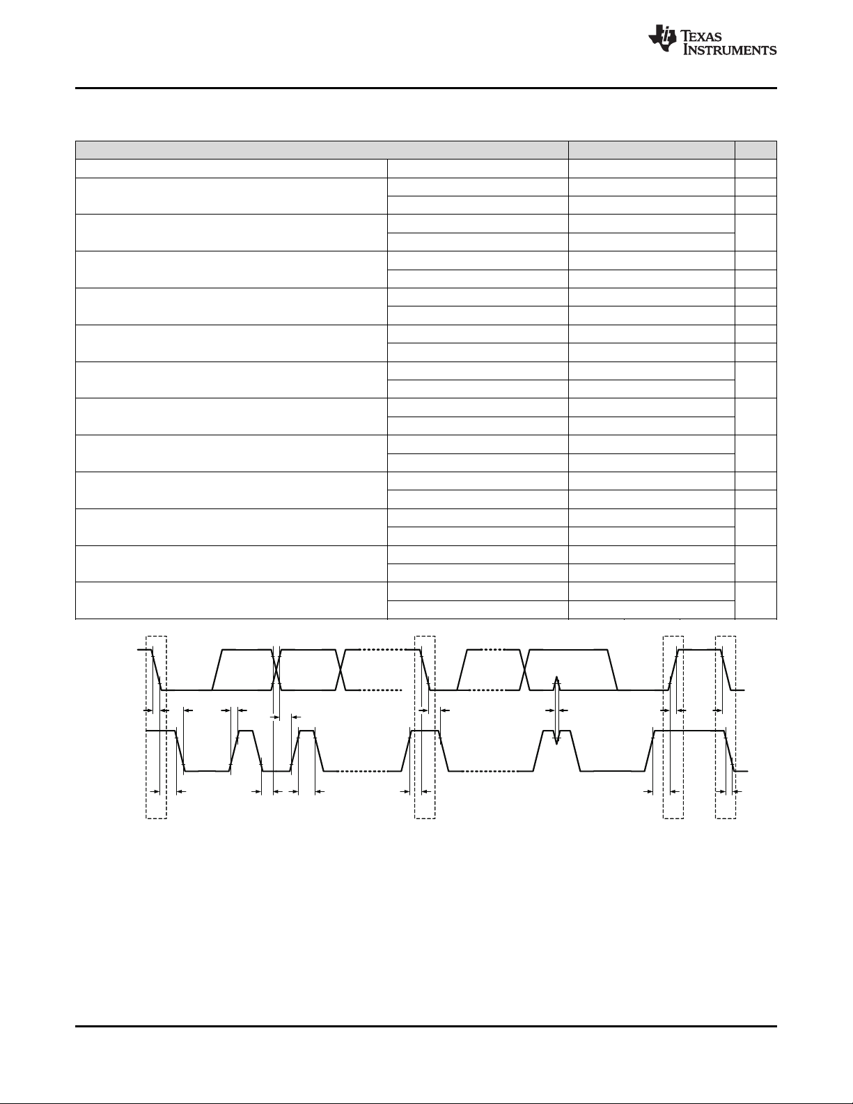
7.6 Timing Requirements: Data Transmission
V
= 3.6 V ±5%, TA= 25ºC, CL= 100 pF (unless otherwise noted)
BAT
f
(SCL)
t
HD;STA
t
LOW
t
HIGH
t
SU;STA
t
HD;DAT
t
SU;DAT
t
r
t
f
t
SU;STO
t
BUF
t
SP
C
b
Serial clock frequency 100 400 kHz
Hold time (repeated) START condition. After this
period, the first clock pulse is generated.
LOW period of the SCL clock
HIGH period of the SCL clock
Set-up time for a repeated START condition
Data hold time
Data set-up time
Rise time of both SDA and SCL signals
Fall time of both SDA and SCL signals
Set-up time for STOP condition
Bus Free Time Between Stop and Start Condition
Pulse width of spikes that must be suppressed by
the input filter
Capacitive load for each bus line
SCL = 100 kHz 4 µs
SCL = 400 kHz 600 ns
SCL = 100 kHz 4.7
SCL = 400 kHz 1.3
SCL = 100 kHz 4 µs
SCL = 400 kHz 600 ns
SCL = 100 kHz 4.7 µs
SCL = 400 kHz 600 ns
SCL = 100 kHz 0 3.45 µs
SCL = 400 kHz 0 900 ns
SCL = 100 kHz 250
SCL = 400 kHz 100
SCL = 100 kHz 1000
SCL = 400 kHz 300
SCL = 100 kHz 300
SCL = 400 kHz 300
SCL = 100 kHz 4 µs
SCL = 400 kHz 600 ns
SCL = 100 kHz 4.7
SCL = 400 kHz 1.3
SCL = 100 kHz n/a n/a
SCL = 400 kHz 0 50
SCL = 100 kHz 400
SCL = 400 kHz 400
www.ti.com
MIN NOM MAX UNIT
µs
ns
ns
ns
µs
ns
pF
12
Submit Documentation Feedback Copyright © 2011–2017, Texas Instruments Incorporated
Figure 1. I2C Data Transmission Timing
Product Folder Links: TPS65185
1.8 ms
(1)
100 ms
(2)
STANDBY
ACTIVE
SLEEP
ACTIVE
UDLY1
UDLY2
UDLY3
UDLY4
300 µs
(maximum)
300 µs
(maximum)
DDLY1
DDLY2 UDLY4
UDLY2
UDLY3
DDLY3
DDLY4
UDLY1
VIN
I2C
PWRUP
WAKEUP
VN
VB
VNEG
VEE
VPOS
VDDH
PWR_GOOD
www.ti.com
TPS65185, TPS651851
SLVSAQ8G –FEBRUARY 2011–REVISED SEPTEMBER 2017
(1) Minimum delay time between WAKEUP rising edge and IC ready to accept I2C transaction.
(2) The device does not enter the SLEEP state until the final discharge delay time has elapsed.
Note: In this example, the first power-up sequence is started by pulling the PWRUP pin high (rising edge). Power-down is
initiated by pulling the WAKEUP pin low (device enters sleep mode after rails are discharged). The second power-up
sequence is initiated by pulling the WAKEUP pin high while the PWRUP pin is also high (power up from sleep to
active).
Figure 2. Power-Up and Power-Down Timing Diagram
Product Folder Links: TPS65185
Submit Documentation FeedbackCopyright © 2011–2017, Texas Instruments Incorporated
13
TPS65185, TPS651851
SLVSAQ8G –FEBRUARY 2011–REVISED SEPTEMBER 2017
7.7 Typical Characteristics
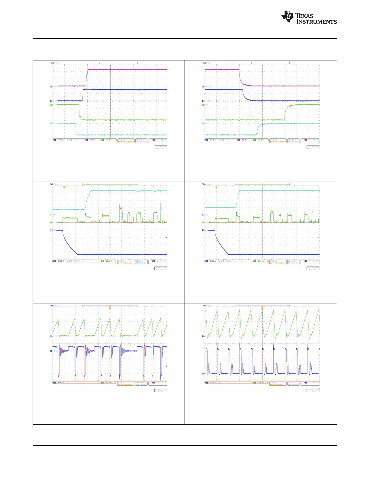
Figure 3. Default Power-Up Sequence Figure 4. Default Power-Down Sequence
www.ti.com
VIN= 3.7 V CIN= 100 µF
Figure 5. Inrush Current
VIN= 3 V R
LOAD, VPOS
No Load on VDDH, VEE
Figure 7. Switching Waveforms, VN
= 330 Ω R
LOAD, VNEG
= 330 Ω
VIN= 5 V CIN= 100 µF
Figure 6. Inrush Current
VIN= 3 V R
LOAD, VPOS
No Load on VDDH, VEE
Figure 8. Switching Waveforms, VB
= 330 Ω R
LOAD, VNEG
= 330 Ω
14
Submit Documentation Feedback Copyright © 2011–2017, Texas Instruments Incorporated
Product Folder Links: TPS65185
-5 0
-4 0
-3 0
-2 0
-1 0
0
1 0
2 0
3 0
4 0
5 0
0 25 50 75 100 1 25 1 50 1 75
C urr e nt [ m A]
VPOS + VNEG[mV]
IPO S= INEG
IPO S s we ep, INE G= 15m A
IPO S= 15m A, IN EG s wee p
0
5
10
15
20
25
1 1.5 2 2.5 3 3.5 4
VIN3P3[V]
R[ ], (VIN3p3-V3P3)/10mAW
www.ti.com
Typical Characteristics (continued)
TPS65185, TPS651851
SLVSAQ8G –FEBRUARY 2011–REVISED SEPTEMBER 2017
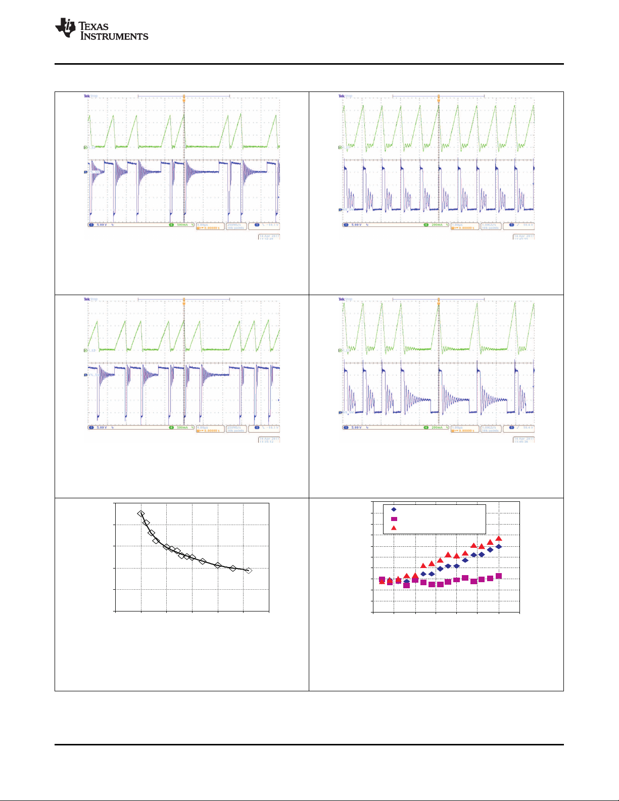
VIN= 3.7 V R
No Load on VDDH, VEE
Figure 9. Switching Waveforms, VN
VIN= 5 V R
No Load on VDDH, VEE
Figure 11. Switching Waveforms, VN
LOAD, VPOS
LOAD, VPOS
= 330 Ω R
= 330 Ω R
LOAD, VNEG
LOAD, VNEG
= 330 Ω
= 330 Ω
VIN= 3.7 V R
No Load on VDDH, VEE
Figure 10. Switching Waveforms, VB
VIN= 5 V R
No Load on VDDH, VEE
Figure 12. Switching Waveforms, VB
LOAD, VPOS
LOAD, VPOS
= 330 Ω R
= 330 Ω R
LOAD, VNEG
LOAD, VNEG
= 330 Ω
= 330 Ω
VIN= 3.7 V I
Figure 13. 3p3V Switch Impedance
LOAD, V3p3
= 10 mA
VIN= 3.7 V
Product Folder Links: TPS65185
Figure 14. Source Driver Supply Tracking
Submit Documentation FeedbackCopyright © 2011–2017, Texas Instruments Incorporated
15
-2
-1. 5
-1
-0. 5
0
0. 5
1
1. 5
2
0 640 12 80 192 0 256 0 320 0 38 40 44 80 5 12 0
Fo rce d Ki ckba c k V ol tag e [m V]
Measurementerror [LSB]
-5
-4
-3
-2
-1
0
1
2
3
4
5
0 64 128 19 2 25 6 320 384 44 8 512
VC OM CO DE
INL [mV]
-0. 2
-0 .15
-0. 1
-0 .05
0
0 .05
0. 1
0 .15
0. 2
0 6 4 1 28 1 92 2 56 3 20 38 4 4 48 51 2
V COM CO DE
DNL[LSB]
TPS65185, TPS651851
SLVSAQ8G –FEBRUARY 2011–REVISED SEPTEMBER 2017
Typical Characteristics (continued)
www.ti.com
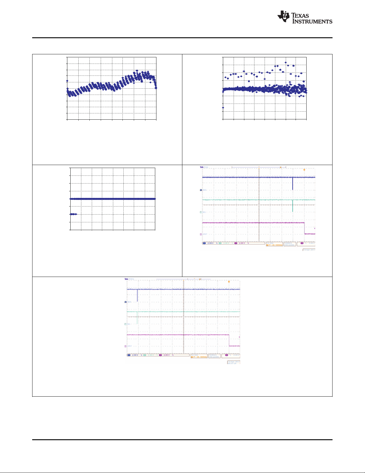
VIN= 3.7 V R
LOAD, VCOM
= 1 kΩ
Figure 15. VCOM Integrated Non-Linearity
VIN= 3.7 V
Figure 17. Kickback Voltage Measurement Error
VIN= 3.7 V R
LOAD, VCOM
= 1 kΩ
Figure 16. VCOM Differential Non-Linearity
VIN= 3.7 V AVG[1:0] = 00 (Single Measurement)
Time from ACQ Bit Set to ACQC Interrupt Received
Figure 18. Kickback Voltage Measurement Timing
16
Submit Documentation Feedback Copyright © 2011–2017, Texas Instruments Incorporated
VIN= 3.7 V AVG[1:0] = 11 (Eight Measurements)
Time from ACQ Bit Set to ACQC Interrupt Received
Figure 19. Kickback Voltage Measurement Timing
Product Folder Links: TPS65185

TPS65185, TPS651851
www.ti.com
SLVSAQ8G –FEBRUARY 2011–REVISED SEPTEMBER 2017
8 Detailed Description
8.1 Overview
The TPS65185x device provides two adjustable LDOs, inverting buck-boost converter, boost converter,
thermistor monitoring, and flexible power-up and power-down sequencing. The system can be supplied by a
regulated input voltage ranging from 3 V to 6 V. The device is characterized across a –10°C to 85°C temperature
range, best suited for personal electronic applications.
The I2C interface provides comprehensive features for using the TPS65185x. All rails can be enabled or
disabled. Power-up and power-down sequences can also be programmed through the I2C interface, as well as
thermistor configuration and interrupt configuration. Voltage adjustment can also be controlled by the I2C
interface.
The adjustable LDOs can supply up to 120 mA (TPS65185) and 200 mA (TPS651851) of current. The default
output voltages for each LDO can be adjusted through the I2C interface. LDO1 (VPOS) and LDO2 (VNEG) track
each other in a way that they are of opposite sign but same magnitude. The sum of VLDO1 and VLOD2 is
specified to be less than 50 mV.
There are two charge pumps: where VDDH and VEE are 10 mA and 12 mA (TPS65185) and VDDH and VEE
are 15 mA and 15 mA (TPS651851) respectively. These charge pumps boost the DC-DC boost converters ±16-V
rails to provide a gate channel supply.
The power good functionality is open-drain output, if any of the four power rails (CP1, CP2, LDO1, LDO2) are not
in regulation, encounters a fault, or is disabled the pin is pulled low. PWR_GOOD remains low if one of the rails
is not enabled by the host and only after all rails are in regulation PWR_GOOD is released to HiZ state (pulled
up by external resistor).
The TPS65185x provides circuitry to bias and measure an external NTC to monitor the display panel
temperature in a range from –10°C to 85°C with and accuracy of ±1°C from 0°C to 50°C. Temperature
measurement are triggered by the controlling host and the last temperature reading is always stored in the
TMST_VALUE register. Interrupts are issued when the temperature exceeds the programmable HOT, or drops
below the programmable COLD threshold, or when the temperature has changed by more than a user-defined
threshold from the baseline value.
This device has the following two package options:
• TPS65185: 48-Pin, 0.5-mm Pitch, 7 mm × 7 mm × 0.9 mm (QFN) RGZ
• TPS65185 and TPS651851: 48-Pin, 0.4 mm Pitch, 6 mm × 6 mm × 0.9 mm (QFN) RSL
Product Folder Links: TPS65185
Submit Documentation FeedbackCopyright © 2011–2017, Texas Instruments Incorporated
17
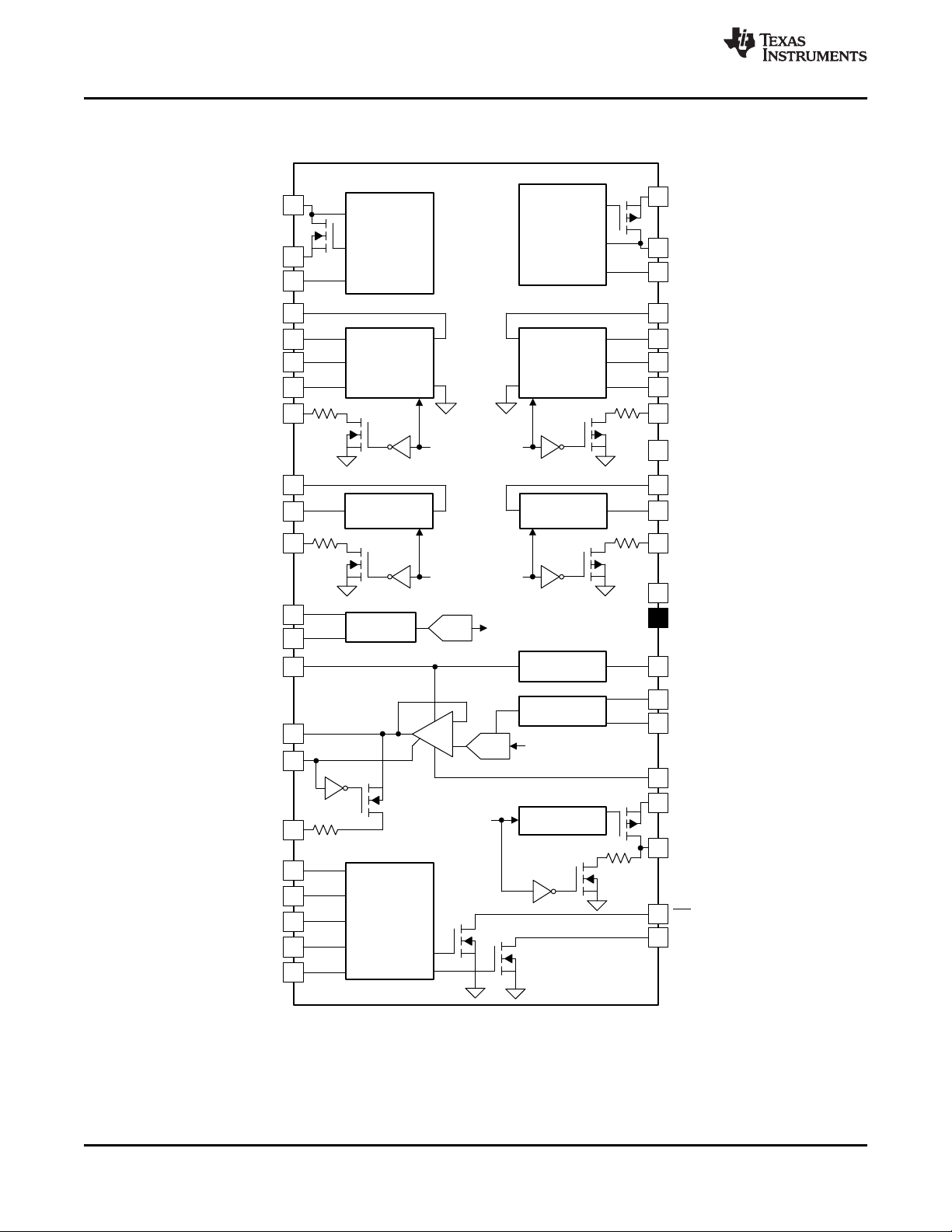
TPS65185x
40
VB_SW
41
PGND1
42
VB
37
VDDH_IN
DCDC1
24
VIN_P
25
VN_SW
26
VN
DCDC2
34
VDDH_D
36
VDDH_DRV
33
VDDH_FB
35
VDDH_DIS
1 k
VDDH
Charge Pump
PGND2
VDDH_EN
PGND2
LDO1
43
VPOS_IN
44
VPOS
19
VPOS_DIS
1 k
VPOS_EN
PGND2
27
VEE_IN
30
VEE_D
28
VEE_DRV
31
VEE_FB
29
VEE_DIS
1 k
VEE
Charge Pump
PGND2
VEE_EN
PGND2
LDO2
4
VNEG_IN
3
VNEG
9
VNEG_DIS
1 k
VNEG_EN
PGND2
22
PBKG
Thermal Pad
32
PGND2
Temperature
Sensor
47
TS
48
AGND2
ADC
TMST_VALUE[7:0]
10
VIN
Internal LDO
Reference
Voltage
7
INT_LDO
15
VCOM
DAC
VCOM[8:0]
+
±
1
VREF
8
AGND1
12
VCOM_CTRL
14
VCOM_DIS
1 k
16
VCOM_PWR
Gate Driver
V3P3_EN
45
VIN3P3
46
V3P3
1 k
Digital Core
6DGND
5WAKEUP
21PWRUP
17SCL
18SDA
2
INT
23
PWR_GOOD
Copyright © 2017, Texas Instruments Incorporated
TPS65185, TPS651851
SLVSAQ8G –FEBRUARY 2011–REVISED SEPTEMBER 2017
8.2 Functional Block Diagram
www.ti.com
18
Submit Documentation Feedback Copyright © 2011–2017, Texas Instruments Incorporated
Product Folder Links: TPS65185

TPS65185, TPS651851
www.ti.com
SLVSAQ8G –FEBRUARY 2011–REVISED SEPTEMBER 2017
8.3 Feature Description
8.3.1 Wake-Up and Power-Up Sequencing
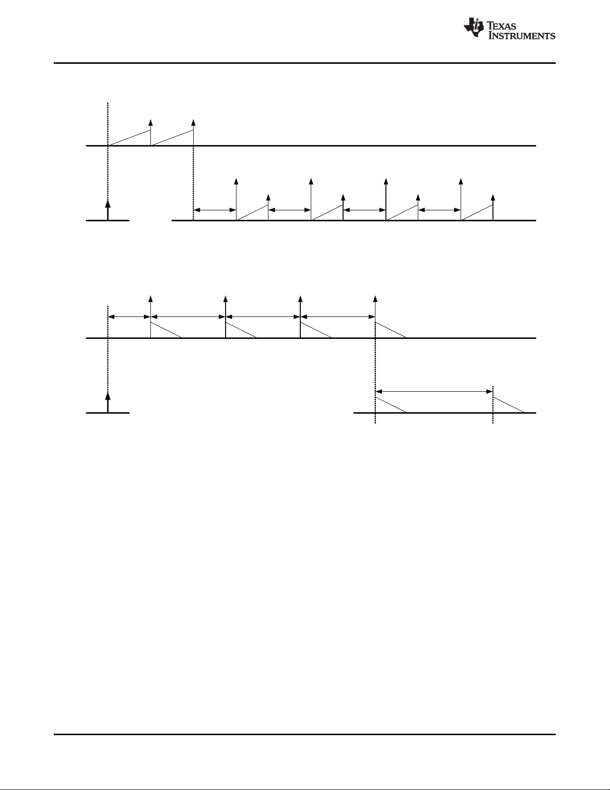
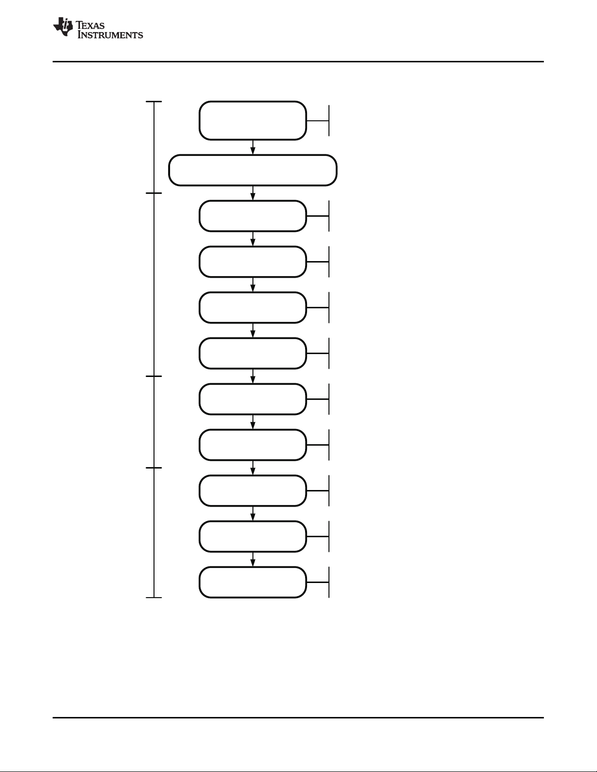
The power-up and power-down order and timing is defined by user register settings. The default settings support
the E Ink Vizplex panel and typically do not need to be changed.
In SLEEP mode the TPS65185x is completely turned off, the I2C registers are reset, and the device does not
accept any I2C transaction. Pull the WAKEUP pin high with the PWRUP pin low and the device enters STANDBY
mode which enables the I2C interface. Write to the UPSEQ0 register to define the order in which the output rails
are enabled at power-up and to the UPSEQ1 registers to define the power-up delays between rails. Finally, set
the ACTIVE bit in the ENABLE register to 1 to execute the power-up sequence and bring up all power rails.
Alternatively pull the PWRUP pin high (rising edge).
After the ACTIVE bit has been set, the negative boost converter (VN) is powered up first, followed by the positive
boost (VB). The positive boost enable is gated by the internal power-good signal of the negative boost. Once VB
is in regulation, it issues an internal power-good signal and after delay time UDLY1 has expired, STROBE1 is
issued. The rail assigned to STROBE1 will power up next and after its power-good signal has been asserted and
delay time UDLY2 has expired, STROBE2 is issued. The sequence continues until STROBE4 has occurred and
the last rail has been enabled.
To power down the device, set the STANDBY bit of the ENABLE register to 1 or pull the PWRUP pin low (falling
edge) and the TPS65185x will power down in the order defined by DWNSEQx registers. The delay times DDLY2,
DDLY3, and DDLY4 are weighted by a factor of DFCTR which allows the user to space out the power down of
the rails to avoid crossing during discharge. DFCTR is located in register DWNSEQ1. The positive boost (VB) is
shut down together with the last rail at STROBE4. However, the negative boost (VN) remains up and running for
another 100 ms (discharge delay) to allow complete discharge of all rails. After the discharge delay, VN is
powered down and the device enters STANDBY or SLEEP mode, depending on the WAKEUP pin.
If either the ACTIVE bit is set or the PWRUP pin is pulled high while the device is powering down, the powerdown sequence (STROBE1-4) is completed first, followed by a power-up sequence. VB and VN may or may not
be powered down and the discharge delay may be cut short depending on the relative timing of STROBE4 to the
new power-up event.
During power-up, if the STANDBY bit is set or the PWRUP pin is pulled low, the power-up sequence is aborted
and the power-down sequence starts immediately.
8.3.2 Dependencies Between Rails
Charge pumps, LDOs, and VCOM driver are dependent on the positive and inverting buck-boost converters and
several dependencies exist that affect the power-up sequencing. These dependencies are listed below.
• Inverting buck-boost (DCDC2) must be in regulation before positive boost (DCDC1) can be enabled.
Internally, DCDC1 enable is gated by DCDC2 power good.
• Positive boost (DCDC1) must be in regulation before LDO2 (VNEG) can be enabled. Internally LDO2 enable
is gated DCDC1 power-good.
• Positive boost (DCDC1) must be in regulation before VCOM can be enabled. Internally VCOM enable is
gated by DCDC1 power good.
• Positive boost (DCDC1) must be in regulation before negative charge pump (CP2) can be enabled. Internally
CP2 enable is gated by DCDC1 power good.
• Positive boost (DCDC1) must be in regulation before positive charge pump (CP1) can be enabled. Internally
CP1 enable is gated by DCDC1 power good.
• LDO2 must be in regulation before LDO1 can be enabled. Internally LDO1 enable is gated by LDO2 power
good.
Submit Documentation FeedbackCopyright © 2011–2017, Texas Instruments Incorporated
Product Folder Links: TPS65185
19
UDLY1
ACTIVE bit
or
WAKEUP high
VN PG VB PG
UDLY2
PG1
STROBE 1 STROBE 2
UDLY3
PG2
STROBE 3
UDLY4
PG3
STROBE 4
PG4
STANDBY bit
or
WAKEUP low
STROBE 2STROBE 1
DDLY1 DDLY2 DDLY3
STROBE 3 STROBE 4
DDLY4
Discharge DELAY
VB
powers up
1strail
powers up
2ndrail
powers up
3ndrail
powers up
4thrail
powers up
4thrail
powers down
3ndrail
powers down
2ndrail
powers down
1strail
powers down
VB
powers down
VN
powers down
VN
powers up
TPS65185, TPS651851
SLVSAQ8G –FEBRUARY 2011–REVISED SEPTEMBER 2017
Feature Description (continued)
www.ti.com
8.3.3 Soft Start
TPS65185x supports soft start for all rails, that is, inrush current is limited during startup of DCDC1, DCDC2,
LDO1, LDO2, CP1 and CP2. If DCDC1 or DCDC2 are unable to reach power-good status within 50 ms, the
corresponding UV flag is set in the interrupt registers, the interrupt pin is pulled low, and the device enters
STANDBY mode. LDO1, LDO2, positive and negative charge pumps also have a 50-ms power-good time-out
limit. If either rail is unable to power up within 50 ms after it has been enabled, the corresponding UV flag is set
and the interrupt pin is pulled low. However, the device will remain in ACTIVE mode in this case.
8.3.4 Active Discharge
TPS65185x provides low-impedance discharge paths for the display power rails (VEE, VNEG, VPOS, VDDH,
and VCOM) which are enabled whenever the corresponding rail is disabled. The discharge paths are connected
to the rails on the PCB which allows adding external resistors to customize the discharge time. However, external
resistors are not required.
TOP: Power-up sequence is defined by assigning strobes to individual rails. STROBE1 is the first strobe to occur after
ACTIVE bit is set and STROBE4 is the last event in the sequence. Strobes are assigned to rails in UPSEQ0 register
and delays between STROBES are defined in UPSEQ1 register.
BOTTOM: Power-down sequence is independent of power-up sequence. Strobes and delay times for power down
sequence are set in DWNSEQ0 and DWNSEQ1 register.
Figure 20. Power-Up and Power-Down Sequence
20
Submit Documentation Feedback Copyright © 2011–2017, Texas Instruments Incorporated
Product Folder Links: TPS65185

TPS65185, TPS651851
www.ti.com
SLVSAQ8G –FEBRUARY 2011–REVISED SEPTEMBER 2017
Feature Description (continued)
Active discharge remains enabled for 100 ms after the last rail has been disabled (STROBE4 has been
executed). During this time the negative boost converter (VN) remains up. After the discharge delay, VN is shut
down and the device enters STANDBY or SLEEP mode, depending on the state of the WAKEUP pin.
8.3.5 VPOS/VNEG Supply Tracking
LDO1 (VPOS) and LDO2 (VNEG) track each other in a way that they are of opposite sign but same magnitude.
The sum of VLDO1 and VLOD2 is specified to be < 50 mV.
8.3.6 V3P3 Power Switch
The integrated power switch is used to cut the 3.3-V supply to the EPD panel and is controlled through the
V3P3_EN pin of the ENABLE register. In SLEEP mode the switch is automatically turned off and its output is
discharged to ground. The default power-up state is OFF. To turn the switch ON, set the V3P3_ENbit to 1.
8.3.7 VCOM Adjustment
VCOM is the output of a power-amplifier with an output voltage range of 0 V to –5.11 V, adjustable in 10-mV
steps. In a typical application VCOM is connected to the VCOM terminal of the EPD panel and the amplifier is
controlled through the VCOM_CTRL pin. With VCOM_CTRL high, the amplifier drives the VCOM pin to the
voltage specified by the VCOM1 and VCOM2 register. When pulled low, the amplifier turns off and VCOM is
actively discharged to ground through VCOM_DIS pin. If active discharge is not desired, simply leave the
VCOM_DIS pin open.
For ease of design, the VCOM_CTRL pin may also be tied to the battery or IO supply. In this case, VCOM is
enabled with STROBE4 during the power-up sequence and disabled on STROBE1 of the power-down sequence.
Therefore VCOM is the last rail to be enabled and the first to be disabled.
8.3.7.1 Kick-Back Voltage Measurement
TPS65185x can perform a voltage measurement on the VCOM pin to determine the kick-back voltage of the
panel. This allows in-system calibration of VCOM. To perform a kick-back voltage measurement, follow these
steps:
• Pull the WAKEUP pin and the PWRUP pin high to enable all output rails.
• Set the HiZ bit in the VCOM2 register. This puts the VCOM pin in a high-impedance state.
• Drive the panel with the Null waveform. Refer to E-Ink specification for detail.
• Set the ACQ bit in the VCOM2 register to 1. This starts the measurement routine.
• When the measurement is complete, the ACQC (Acquisition Complete) bit in the INT1 register is set and the
nINT pin is pulled low.
• The measurement result is stored in the VCOM[8:0] bits of the VCOM1 and VCOM2 register.
The measurement result is not automatically programmed into nonvolatile memory. Changing the power-up
default is described in the following paragraph.
Product Folder Links: TPS65185
Submit Documentation FeedbackCopyright © 2011–2017, Texas Instruments Incorporated
21

VIN
10 µF
VCOM_PWR
4.7 µF
To panel back-plane
(–0.5 V to 5 V, 15 mA)–
From Input Supply
(3 V to 6 V)
4.7 µF
VREF
AGND1
DAC
VCOM
VCOM[8:0]
VCOM_CTRL
4.7 µF
From uC
VREF
4.7 µF
INT_LDO
INT_LDO
From VN (–17 V)
TPS65185, TPS651851
SLVSAQ8G –FEBRUARY 2011–REVISED SEPTEMBER 2017
www.ti.com
Feature Description (continued)
8.3.7.2 Storing the VCOM Power-Up Default Value in Memory
The power-up default value of VCOM can be user-set and programmed into nonvolatile memory. To do so, write
the default value to the VCOM[8:0] bits of the VCOM1 and VCOM2 register, then set the PROG bit in VCOM2
register to 1. First, all power rails are shut down, then the VCOM[8:0] value is committed to nonvolatile memory
such that it becomes the new power-up default. Once programming is complete, the PRGC bit in the INT1
register is set and the nINT pin is pulled low. To verify that the new value has been saved properly, first write the
VCOM[8:0] bits to 0x000h, then pull the WAKEUP pin low. After the WAKEUP pin is pulled back high, read the
VCOM[8:0] bits to verify that the new default value is correct.
Figure 21. Block Diagram of VCOM Circuit
22
Submit Documentation Feedback Copyright © 2011–2017, Texas Instruments Incorporated
Product Folder Links: TPS65185
Pull WAKEUP= HIGH
Pull PWRUP= HIGH
Write HiZ = 1
Device enters ACTIVE mode
All power rails are up except VCOM
VCOM pin is in HiZ state
Processor drives panel with NULL waveform
Write ACQ = 1 Starts A/D conversion
Wait for ACQC interrupt
Indicates A/D conversion is complete
If AVG[1:0] is <> 00, interrupt is issed
after all conversions are complete and
average has been calcutated.
Read result from VCOM1/2
registers
Pull PWRUP= LOW
Write HiZ = 0
Check result and decide to keep the
value or repeat measurment.
Device enters STANDBY mode
Write PROG= 1
Starts the EEPROM programming cycle.
Power must not be interrupted.
Wait for PRGC interrupt Indicates programming is complete
Pull WAKEUP= LOW Device enters SLEEP mode
Pull WAKEUP= HIGH Device enters STANDBY mode
Read VCOM[8:0]
Compare against written value to
confirm new default has been
programmed correctly.
SETUP
MEASUREMENT
PROGRAMMING
VERIFICATION
www.ti.com
Feature Description (continued)
TPS65185, TPS651851
SLVSAQ8G –FEBRUARY 2011–REVISED SEPTEMBER 2017
Figure 22. VCOM Calibration Flow
Product Folder Links: TPS65185
Submit Documentation FeedbackCopyright © 2011–2017, Texas Instruments Incorporated
23

TPS65185, TPS651851
SLVSAQ8G –FEBRUARY 2011–REVISED SEPTEMBER 2017
www.ti.com
Feature Description (continued)
8.3.8 Fault Handling And Recovery
The TPS65185x monitors input/output voltages and die temperature. The device will take action if operating
conditions are outside normal limits when the following is encountered:
• Thermal Shutdown (TSD)
• Positive Boost Under Voltage (VB_UV)
• Inverting Buck-Boost Under Voltage (VN_UV)
• Input Undervoltage Lockout (UVLO)
it shuts down all power rails and enters STANDBY mode. Shut-down follows the order defined by DWNSEQx
registers. The exception is VCOM fault witch leads to immediate shutdown of all rails. Once a fault is detected,
the PWR_GOOD and nINT pins are pulled low and the corresponding interrupt bit is set in the interrupt register.
Power rails cannot be re-enabled unless the interrupt bits have been cleared by reading the INT1 and INT2
register. Alternatively, toggling the WAKEUP pin also resets the interrupt bits. As the PWRUP input is edge
sensitive, the host must toggle the PWRUP pin to re-enable the rails through GPIO control, i.e. it must bring the
PWRUP pin low before asserting it again. Alternatively rails can be re-enabled through the I2C interface.
Whenever the TPS65185x encounters undervoltage on VNEG (VNEG_UV), VPOS (VPOS_UV), VEE (VEE_UV)
or VDDH (VDDH_UV), rails are not shut down but the PWR_GOOD and nINT is pulled low with the
corresponding interrupt bit set. The device remains in ACTIVE mode and recovers automatically once the fault
has been removed.
8.3.9 Power Good Pin
The power good pin (PWR_GOOD) is an open-drain output that is pulled high (by an external pullup resistor)
when all four power rails (CP1, CP2, LDO1, LDO2) are in regulation and is pulled low if any of the rails
encounters a fault or is disabled. PWR_GOOD remains low if one of the rails is not enabled by the host and only
after all rails are in regulation PWR_GOOD is released to HiZ state (pulled up by external resistor).
8.3.10 Interrupt Pin
The interrupt pin (nINT) is an open drain output that is pulled low whenever one or more of the INT1 or INT2 bits
are set. The nINT pin is released (returns to HiZ state) and fault bits are cleared once the register with the set bit
has been read by the host. If the fault persists, the nINT pin will be pulled low again after a maximum of 32 µs.
Interrupt events can be masked by resetting the corresponding enable bit in the INT_EN1 and INT_EN2 register,
that is, the user can determine which events cause the nINT pin to be pulled low. The status of the enable bits
affects the nINT pin only and has no effect on any of the protection and monitoring circuits or the INT1/INT2 bits
themselves.
Persisting faults such as thermal shutdown can cause the nINT pin to be pulled low for an extended period of
time which can keep the host in a loop trying to resolve the interrupt. If this behavior is not desired, set the
corresponding mask bit after receiving the interrupt and keep polling the INT1 and INT2 register to see when the
fault condition has disappeared. After the fault is resolved, unmask the interrupt bit again.
8.3.11 Panel Temperature Monitoring
The TPS65185x provides circuitry to bias and measure an external Negative Temperature Coefficient Resistor
(NTC) to monitor the display panel temperature in a range from –10°C to 85°C with and accuracy of ±1°C from
0°C to 50°C. Temperature measurement must be triggered by the controlling host and the last temperature
reading is always stored in the TMST_VALUE register. Interrupts are issued when the temperature exceeds the
programmable HOT, or drops below the programmable COLD threshold, or when the temperature has changed
by more than a user-defined threshold from the baseline value. Details are explained in Hot, Cold, and
Temperature-Change Interrupts.
24
Submit Documentation Feedback Copyright © 2011–2017, Texas Instruments Incorporated
Product Folder Links: TPS65185
7.307k
2.25V
43k 10k NTC
10
ADCDigital
TS
AGND2
TPS65185, TPS651851
www.ti.com
SLVSAQ8G –FEBRUARY 2011–REVISED SEPTEMBER 2017
Feature Description (continued)
8.3.11.1 NTC Bias Circuit
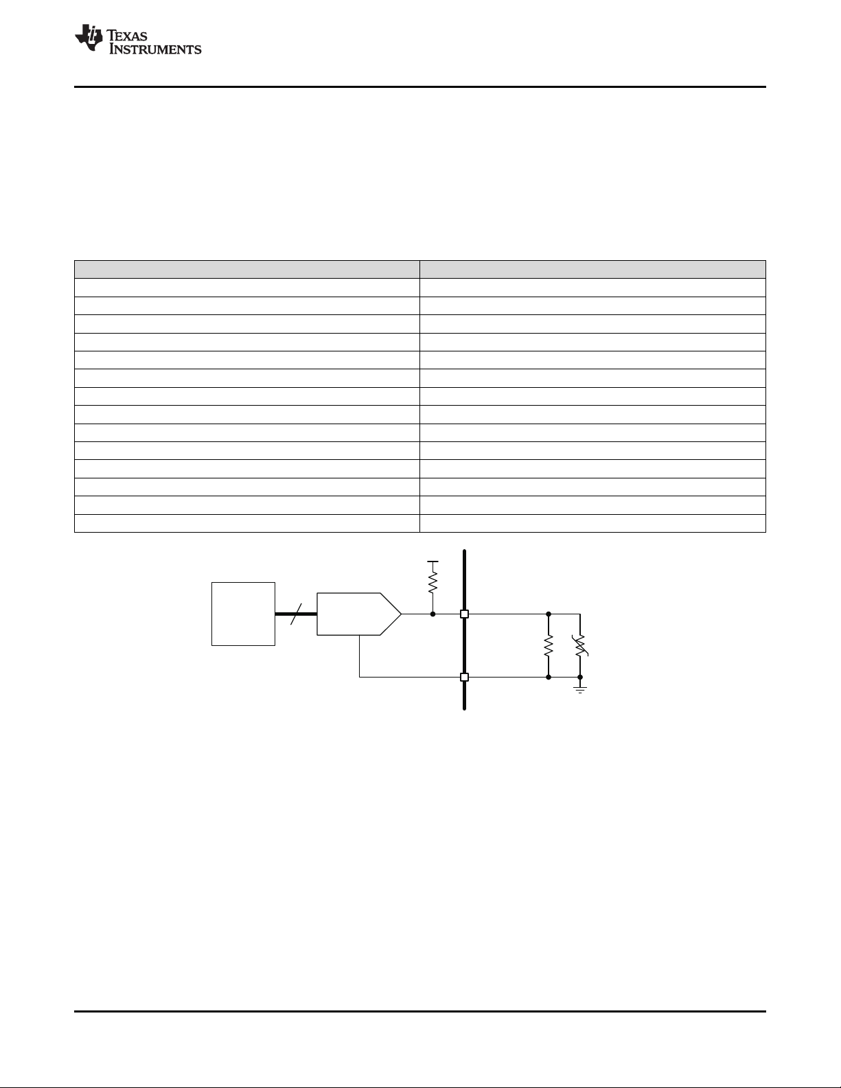
Figure 23 below shows the block diagram of the NTC bias and measurement circuit. The NTC is biased from an
internally generated 2.25-V reference voltage through an integrated 7.307-kΩ bias resistor. A 43-kΩ resistor is
connected parallel to the NTC to linearize the temperature response curve. The circuit is designed to work with a
nominal 10-kΩ NTC and achieves accuracy of ±1°C from 0°C to 50°C. The voltage drop across the NTC is
digitized by a 10-bit SAR ADC and translated into an 8-bit two’s complement by digital per Table 1.
Table 1. ADC Output Value vs Temperature
TEMPERATURE TMST_VALUE[7:0]
< –10°C 1111 0110
–10°C 1111 0110
–9°C 1111 0111
... ...
–2°C 1111 1110
–1°C 1111 1111
0°C 0000 0000
1°C 0000 0001
2°C 0000 0010
... ...
25°C 0001 1001
...
85°C 0101 0101
> 85°C 0101 0101
Figure 23. NTC Bias and Measurement Circuit
A temperature measurement is triggered by setting the READ_THERM bit of the TMST1 register to 1.During the
A/D conversion the CONV_END bit of the TMST1 register reads 0, otherwise it reads 1. At the end of the A/D
conversion the EOC bit in the INT2 register is set and the temperature value is available in the TMST_VALUE
register.
Product Folder Links: TPS65185
Submit Documentation FeedbackCopyright © 2011–2017, Texas Instruments Incorporated
25

TPS65185, TPS651851
SLVSAQ8G –FEBRUARY 2011–REVISED SEPTEMBER 2017
www.ti.com
8.3.11.2 Hot, Cold, and Temperature-Change Interrupts
Each temperature acquisition is compared against the programmable TMST_HOT and TMST_COLD thresholds
and to the baseline temperature, to determine if the display is within allowed operating temperature range and if
the temperature has changed by more than a user-defined threshold since the last update. The first temperature
reading after the WAKEUP pin has been pulled high automatically becomes the baseline temperature. Any
subsequent reading is compared against the baseline temperature. If the difference is equal or greater than the
threshold value, an interrupt is issued (DTX bit in register INT1 is set to 1) and the latest value becomes the new
baseline. If the difference is less than the threshold value, no action is taken. The threshold value is defined by
DT[1:0] bits in the TMST1 register and has a default value of ±2°C. In summary:
• When the temperature is equal or less than the TMST_COLD[3:0] threshold, the TMST_COLD interrupt bit of
the INT1 register is set, and the nINT pin is pulled low.
• When the temperature is greater than TMST_COLD but lower then TMST_HOT, no action is taken.
• When the temperature is equal or greater than the TMST_HOT[3:0] threshold, the TMST_HOT interrupt bit of
the INT1 register is set, and the nINT pin is pulled low.
• If the last temperature is different from the baseline temperature by ±2°C (default) or more, the DTX interrupt
bit of the INT1 register is set. The latest temperature becomes the new baseline temperature. By default the
DTX interrupt is disabled, that is, the nINT pin is not pulled low unless the DTX_EN bit was previously set
high.
• If the last temperature change is less than ±2°C (default), no action is taken.
8.3.11.3 Typical Application of the Temperature Monitor
In a typical application the temperature monitor and interrupts are used in the following manner:
• After the WAKEUP pin has been pulled high, the Application Processor (AP) writes 0x80h to the TMST1
register (address 0x0Dh). This starts the temperature measurement.
• The AP waits for the EOC interrupt. Alternatively the AP can poll the CONV_END bit in register TMST1. This
will notify the AP that the A/D conversion is complete and the new temperature reading is available in the
TMST_VALUE register (address (0x00h).
• The AP reads the temperature value from the TMST_VALUE register (address (0x00h).
• If the temperature changes by ±2°C (default) or more from the first reading, the processor is notified by the
DTX interrupt. The A/P may or may not decide to select a different set of wave forms to drive the panel.
• If the temperature is outside the allowed operating range of the panel, the processor is notified by the THOT
and TCOLD interrupts, respectively. It may or may not decide to continue with the page update.
• Once an overtemperature or undertemperature has been detected, the AP must reset the TMST_HOT_EN or
TMST_COLD_EN bits, respectively, to avoid the nINT pin to be continuously pulled low. The TMST_HOT and
TMST_COLD interrupt bits then must be polled continuously, to determine when the panel temperature
recovers to the normal operating range. Once the temperature has recovered, the TMST_HOT_EN or
TMST_COLD_EN bits must be set to 1 again and normal operation can resume.
26
Submit Documentation Feedback Copyright © 2011–2017, Texas Instruments Incorporated
Product Folder Links: TPS65185

TPS65185, TPS651851
www.ti.com
SLVSAQ8G –FEBRUARY 2011–REVISED SEPTEMBER 2017
8.4 Device Functional Modes
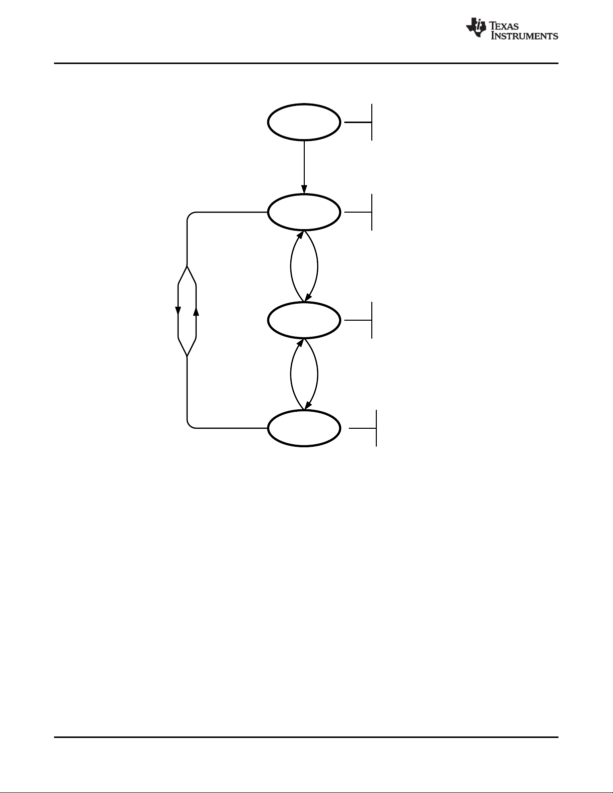
The TPS65185x has three modes of operation, SLEEP, STANDBY, and ACTIVE. SLEEP mode is the lowestpower mode in which all internal circuitry is turned off. In STANDBY, all power rails are shut down but the device
is ready to accept commands through the I2C interface. In ACTIVE mode one or more power rails are enabled.
8.4.1 SLEEP
This is the lowest power mode of operation. All internal circuitry is turned off, registers are reset to default values
and the device does not respond to I2C communications. TPS65185x enters SLEEP mode whenever WAKEUP
pin is pulled low.
8.4.2 STANDBY
In STANDBY all internal support circuitry is powered up and the device is ready to accept commands through the
I2C interface but none of the power rails are enabled. The device enters STANDBY mode when the WAKEUP pin
is pulled high and either the PWRUP pin is pulled low or the STANDBY bit is set. The device also enters
STANDBY mode if input UVLO, positive boost undervoltage (VB_UV), or inverting buck-boost undervoltage
(VN_UV) is detected, thermal shutdown occurs, or the PROG bit is set (see Figure 22).
8.4.3 ACTIVE
The device is in ACTIVE mode when any of the output rails are enabled and no fault condition is present. This is
the normal mode of operation while the device is powered up.
8.4.4 Mode Transitions
8.4.4.1 SLEEP → ACTIVE
WAKEUP pin is pulled high with PWRUP pin high. Rails come up in the order defined by the UPSEQx registers
(OK to tie WAKEUP and PWRUP pin together).
8.4.4.2 SLEEP → STANDBY
WAKEUP pin is pulled high with PWRUP pin low. Rails will remain powered down.
8.4.4.3 STANDBY → ACTIVE
WAKEUP pin is high and PWRRUP pin is pulled high (rising edge) or the ACTIVE bit is set. Output rails will
power up in the order defined by the UPSEQx registers.
8.4.4.4 ACTIVE → STANDBY
WAKEUP pin is high and STANDBY bit is set or PWRUP pin is pulled low (falling edge). Rails are shut down in
the order defined by DWNSEQx registers. Device also enters STANDBY in the event of thermal shutdown (TSD),
UVLO, positive boost or inverting buck-boost undervoltage (UV), VCOM fault (VCOMF), or when the PROG bit is
set (see Figure 22).
8.4.4.5 STANDBY → SLEEP
WAKEUP pin is pulled low while none of the output rails are enabled.
8.4.4.6 ACTIVE → SLEEP
WAKEUP pin is pulled low while at least one output rail is enabled. Rails are shut down in the order defined by
DWNSEQx registers.
Product Folder Links: TPS65185
Submit Documentation FeedbackCopyright © 2011–2017, Texas Instruments Incorporated
27
SLEEP
ACTIVE
Rails = ON
I2C = YES
POWER DOWN
WAKEUP = high &
PWRUP= low
All rails = OFF
V3P3 switch= OFF
I2C = NO
Registers à default
Battery removed
STANDBY
WAKEUP = high &
(ACTIVE bit= 1 || PWRUP( ) )
All rails = OFF
I2C = YES
WAKEUP = high &
(STANDBY bit = 1||
PWRUP(¯) || FAULT )
WAKEUP = low
WAKEUP = high & PWRUP = high
WAKEUP = l ow
¯
TPS65185, TPS651851
SLVSAQ8G –FEBRUARY 2011–REVISED SEPTEMBER 2017
Device Functional Modes (continued)
www.ti.com
NOTES:
||, & = logic OR, and AND.
(↑), (↓) = rising edge, falling edge
UVLO = Undervoltage Lockout
TSD = Thermal Shutdown
UV = Undervoltage
FAULT = UVLO || TSD || BOOST UV || VCOM fault
28
Submit Documentation Feedback Copyright © 2011–2017, Texas Instruments Incorporated
Figure 24. Global State Diagram
Product Folder Links: TPS65185

S A6 A5 A4 A3 A2 A1 A0 A S7 S6 S5 S4 S3 S2 S1 S0 A D7 D6 D5 D4 D3 D2 D1 D0 A P
S AStart Condition Acknowledge A6 A0... Device Address
R/nW
Read / not Write
S7 S0... Sub-Address
D7 D0... Data
P Stop Condition
R/nW
Slave Address + R/nW Reg Address Data
TPS65185, TPS651851
www.ti.com
SLVSAQ8G –FEBRUARY 2011–REVISED SEPTEMBER 2017
8.5 Programming
8.5.1 I2C Bus Operation
The TPS65185x hosts a slave I2C interface that supports data rates up to 400 kbit/s and auto-increment
addressing and is compliant to I2C standard 3.0.
Figure 25. Subaddress in I2C Transmission
The I2C Bus is a communications link between a controller and a series of slave terminals. The link is established
using a two-wire bus consisting of a serial clock signal (SCL) and a serial data signal (SDA). The serial clock is
sourced from the controller in all cases where the serial data line is bi-directional for data communication
between the controller and the slave terminals. Each device has an open drain output to transmit data on the
serial data line. An external pullup resistor must be placed on the serial data line to pull the drain output high
during data transmission.
Data transmission is initiated with a start bit from the controller as shown in Figure 27. The start condition is
recognized when the SDA line transitions from high to low during the high portion of the SCL signal. Upon
reception of a start bit, the device will receive serial data on the SDA input and check for valid address and
control information. If the appropriate slave address bits are set for the device, then the device will issue an
acknowledge pulse and prepare to receive the register address. Depending on the R/nW bit, the next byte
received from the master is written to the addressed register (R/nW = 0) or the device responds with 8-bit data
from the register (R/nW = 1). Data transmission is completed by either the reception of a stop condition or the
reception of the data word sent to the device. A stop condition is recognized as a low to high transition of the
SDA input during the high portion of the SCL signal. All other transitions of the SDA line must occur during the
low portion of the SCL signal. An acknowledge is issued after the reception of valid address, sub-address, and
data words. The I2C interfaces will auto-sequence through register addresses, so that multiple data words can be
sent for a given I2C transmission. See Figure 26 and Figure 27 for details.
Product Folder Links: TPS65185
Submit Documentation FeedbackCopyright © 2011–2017, Texas Instruments Incorporated
29
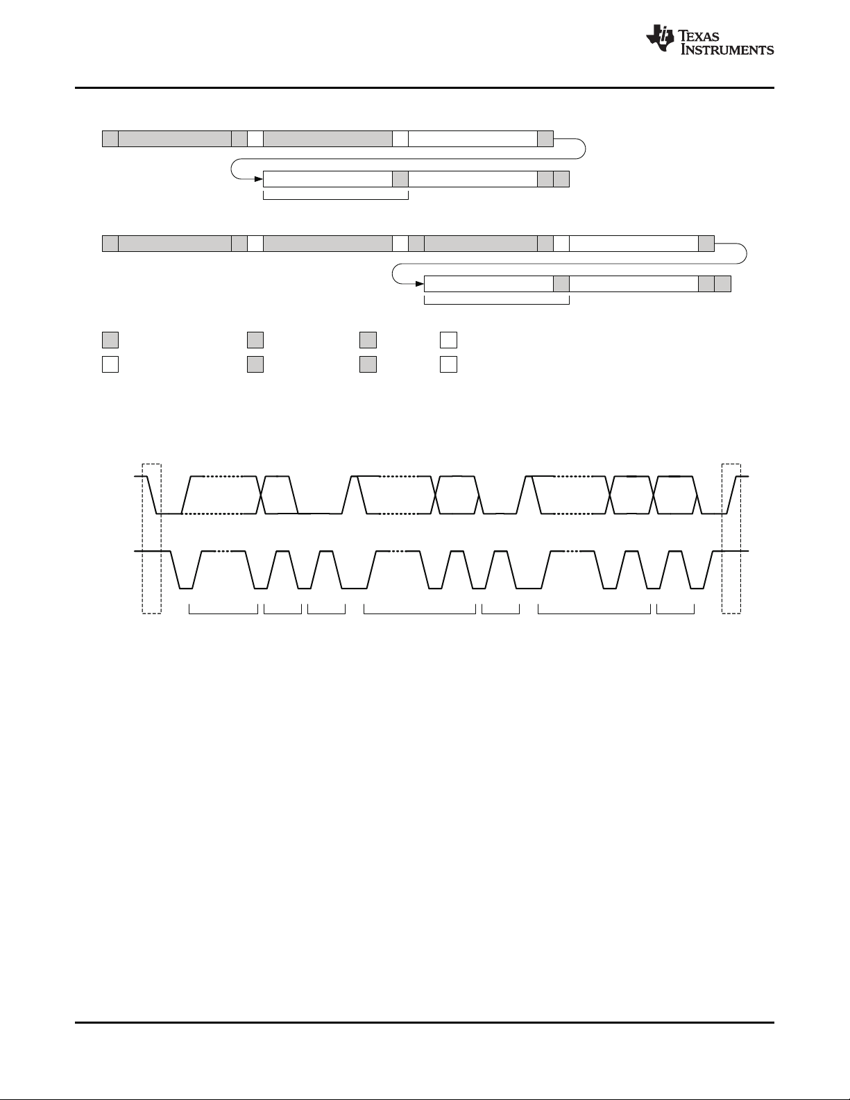
S
1-7 8 9 1-7 8 9 1-7 8 9
P
ADDRESS R/W ACK DATA ACK DATA
ACK/
nACK
STOPSTART
SDA
SCL
SLAVE ADDRESS W A REG ADDRESS A SLAVE ADDRESS R A DATA
REGADDR
AS
DATA
REGADDR +n
A DATA
REGADDR +n+1
Ā P
From master to slave
From slave to master
S
W AP
Start
Write (low) AcknowlegeStop
R Read (high)
S
Ā Not Acknowlege
n bytes + ACK
SLAVE ADDRESS W A REG ADDRESS A DATA
REGADDR
AS
DATA
SUBADDR +n
A DATA
SUBADDR +n+1
Ā P
n bytes + ACK
TPS65185, TPS651851
SLVSAQ8G –FEBRUARY 2011–REVISED SEPTEMBER 2017
Programming (continued)
TOP: Master writes data to slave.
BOTTOM: Master reads data from slave.
Figure 26. I2C Data Protocol
www.ti.com
Figure 27. I2C Start/Stop/Acknowledge Protocol
30
Submit Documentation Feedback Copyright © 2011–2017, Texas Instruments Incorporated
Product Folder Links: TPS65185

www.ti.com
SLVSAQ8G –FEBRUARY 2011–REVISED SEPTEMBER 2017
8.6 Register Maps
Table 2. Register Address Map
Address Acronym Register Name Section
0x00h TMST_VALUE Thermistor value read by ADC Go
0x01h ENABLE Enable/disable bits for regulators Go
0x02h VADJ VPOS/VNEG voltage adjustment Go
0x03h VCOM1 Voltage settings for VCOM Go
0x04h VCOM2 Voltage settings for VCOM + control Go
0x05h INT_EN1 Interrupt enable group1 Go
0x06h INT_EN2 Interrupt enable group2 Go
0x07h INT1 Interrupt group1 Go
0x08h INT2 Interrupt group2 Go
0x09h UPSEQ0 Power-up strobe assignment Go
0x0Ah UPSEQ1 Power-up sequence delay times Go
0x0Bh DWNSEQ0 Power-down strobe assignment Go
0x0Ch DWNSEQ1 Power-down sequence delay times Go
0x0Dh TMST1 Thermistor configuration Go
0x0Eh TMST2 Thermistor hot temp set Go
0x0Fh PG Power good status each rails Go
0x10h REVID Device revision ID information Go
TPS65185, TPS651851
8.6.1 Thermistor Readout (TMST_VALUE) Register (address = 0x00h) [reset = N/A]
Figure 28. TMST_VALUE Register
7 6 5 4 3 2 1 0
TMST_VALUE[7:0]
R-N/A
LEGEND: R/W = Read/Write; R = Read only; -n = value after reset
Table 3. TMST_VALUE Register Field Descriptions
Bit Field Type Reset Description
7-0 TMST_VALUE R N/A Temperature read-out
F6h = < –10°C
F7h = –9°C
...
FEh = –2°C
FFh = –1°C
0h = 0°C
1h = 1°C
2h = 2°C
...
19h = 25°C
...
55h = > 85°C
Product Folder Links: TPS65185
Submit Documentation FeedbackCopyright © 2011–2017, Texas Instruments Incorporated
31

TPS65185, TPS651851
SLVSAQ8G –FEBRUARY 2011–REVISED SEPTEMBER 2017
8.6.2 Enable (ENABLE) Register (address = 0x01h) [reset = 0h]
Figure 29. ENABLE Register
7 6 5 4 3 2 1 0
ACTIVE STANDBY V3P3_EN VCOM_EN VDDH_EN VPOS_EN VEE_EN VNEG_EN
R/W-0h R/W-0h R/W-0h R/W-0h R/W-0h R/W-0h R/W-0h R/W-0h
LEGEND: R/W = Read/Write; R = Read only; -n = value after reset
Table 4. ENABLE Register Field Descriptions
Bit Field Type Reset Description
7 ACTIVE R/W 0h STANDBY to ACTIVE transition bit
0h = no effect
1h = Transition from STANDBY to ACTIVE mode. Rails power
up as defined by UPSEQx registers
NOTE: After transition bit is cleared automatically
6 STANDBY R/W 0h STANDBY to ACTIVE transition bit
0h = no effect
1h = Transition from STANDBY to ACTIVE mode. Rails power
up as defined by DWNSEQx registers
NOTE: After transition bit is cleared automatically. STANDBY bit
has priority over ACTIVE.
5 V3P3_EN R/W 0h VIN3P3 to V3P3 switch enable
0h = Switch is OFF
1h = Switch is ON
4 VCOM_EN R/W 0h VCOM buffer enable
0h = Disabled
1h = Enabled
3 VDDH_EN R/W 0h VDDH charge pump enable
0h = Disabled
1h = Enabled
2 VPOS_EN R/W 0h VPOS LDO regulator enable
0h = Disabled
1h = Enabled
NOTE: VPOS cannot be enabled before VNEG is enabled.
1 VEE_EN R/W 0h VEE charge pump enable
0h = Disabled
1h = Enabled
0 VNEG_EN R/W 0h VNEG LDO regulator enable
0h = Disabled
1h = Enabled
NOTE: When VNEG is disabled VPOS will also be disabled.
www.ti.com
32
Submit Documentation Feedback Copyright © 2011–2017, Texas Instruments Incorporated
Product Folder Links: TPS65185

TPS65185, TPS651851
www.ti.com
SLVSAQ8G –FEBRUARY 2011–REVISED SEPTEMBER 2017
8.6.3 Voltage Adjustment (VADJ) Register (address = 0x02h) [reset = 23h]
Figure 30. VADJ Register
7 6 5 4 3 2 1 0
Not used Not used Not used Not used Not used VSET[2:0]
R/W-0h R/W-0h R/W-1h R/W-0h R-0h R/W-3h
LEGEND: R/W = Read/Write; R = Read only; -n = value after reset
Table 5. VADJ Register Field Descriptions
Bit Field Type Reset Description
7 Not used R/W 0h N/A
6 Not used R/W 0h N/A
5 Not used R/W 1h N/A
4 Not used R/W 0h N/A
3 Not used R 0h N/A
2-0 VSET R/W 3h VPOS and VNEG voltage setting
0h = not valid
1h = not valid
2h = not valid
3h = ±15.000 V
4h = ±14.750 V
5h = ±14.500 V
6h = ±14.250 V
7h = reserved
Product Folder Links: TPS65185
Submit Documentation FeedbackCopyright © 2011–2017, Texas Instruments Incorporated
33

TPS65185, TPS651851
SLVSAQ8G –FEBRUARY 2011–REVISED SEPTEMBER 2017
8.6.4 VCOM 1 (VCOM1) Register (address = 0x03h) [reset = 7Dh]
Figure 31. VCOM1 Register
7 6 5 4 3 2 1 0
VCOM[7:0]
R/W-7Dh
LEGEND: R/W = Read/Write; R = Read only; -n = value after reset
Table 6. VCOM1 Register Field Descriptions
Bit Field Type Reset Description
7-0 VCOM R/W 7Dh VCOM voltage, least significant byte. See VCOM 2 (VCOM2)
Register (address = 0x04h) [reset = 04h] for details.
www.ti.com
34
Submit Documentation Feedback Copyright © 2011–2017, Texas Instruments Incorporated
Product Folder Links: TPS65185

TPS65185, TPS651851
www.ti.com
SLVSAQ8G –FEBRUARY 2011–REVISED SEPTEMBER 2017
8.6.5 VCOM 2 (VCOM2) Register (address = 0x04h) [reset = 04h]
Figure 32. VCOM2 Register
7 6 5 4 3 2 1 0
ACQ PROG HiZ AVG[1:0] Not used Not used VCOM[8]
R/W-0h R/W-0h R/W-0h R/W-0h R/W-1h R/W-0h R/W-0h
LEGEND: R/W = Read/Write; R = Read only; -n = value after reset
Table 7. VCOM2 Register Field Descriptions
Bit Field Type Reset Description
7 ACQ R/W 0h Kick-back voltage acquisition bit
6 PROG R/W 0h VCOM programming bit
5 HiZ R/W 0h VCOM HiZ bit
4-3 AVG R/W 0h Number of acquisitions that is averaged to a single kick-back
2 Not used R/W 1h N/A
1 Not used R/W 0h N/A
0 VCOM R/W 0h VCOM voltage adjustment
0h = No effect
1h = Starts kick-back voltage measurement routine
NOTE: After measurement is complete bit is cleared automatically
and measurement result is reflected in VCOM[8:0] bits.
0h = No effect
1h = VCOM[8:0] value is committed to nonvolatile memory and
becomes new power-up default
NOTE: After programming bit is cleared automatically and
TPS65185x will enter STANDBY mode.
1h = VCOM pin is placed into hi-impedance state to allow VCOM
measurement
0h = VCOM amplifier is connected to VCOM pin
voltage measurement
0h = 1x
1h = 2x
2h = 4x
3h = 8x
NOTE: When the ACQ bit is set, the state machine repeat the A/D
conversion of the kick-back voltage AVD[1:0] times and returns a
single, averaged, value to VCOM[8:0]
VCOM = VCOM[8:0] x –10 mV in the range from 0 mV to –5.110 V
0h = –0 mV
1h = –10 mV
2h = –20 mV
...
7Dh = –1250 mV
...
1FEh = –5100 mV
1FFh = –5110 mV
Product Folder Links: TPS65185
Submit Documentation FeedbackCopyright © 2011–2017, Texas Instruments Incorporated
35

TPS65185, TPS651851
SLVSAQ8G –FEBRUARY 2011–REVISED SEPTEMBER 2017
8.6.6 Interrupt Enable 1 (INT_EN1) Register (address = 0x05h) [reset = 7Fh]
Figure 33. INT_EN1 Register
7 6 5 4 3 2 1 0
DTX_EN TSD_EN HOT_EN TMST_HOT_ENTMST_COLD_ENUVLO_EN ACQC_EN PRGC_EN
R-0h R/W-1h R/W-1h R/W-1h R/W-1h R/W-1h R-1h R-1h
LEGEND: R/W = Read/Write; R = Read only; -n = value after reset
Table 8. INT_EN1 Register Field Descriptions
Bit Field Type Reset Description
7 DTX_EN R 0h Panel temperature-change interrupt enable
0h = Disabled
1h = Enabled
NOTE: Enabled means nINT pin is pulled low when interrupt
occurs.
Disabled means nINT pin is not pulled low when interrupt
occurs.
6 TSD_EN R/W 1h Thermal shutdown interrupt enable
0h = Disabled
1h = Enabled
NOTE: Enabled means nINT pin is pulled low when interrupt
occurs.
Disabled means nINT pin is not pulled low when interrupt
occurs.
5 HOT_EN R/W 1h Thermal shutdown early warning enable
0h = Disabled
1h = Enabled
NOTE: Enabled means nINT pin is pulled low when interrupt
occurs.
Disabled means nINT pin is not pulled low when interrupt
occurs.
4 TMST_HOT_EN R/W 1h Thermistor hot interrupt enable
0h = Disabled
1h = Enabled
NOTE: Enabled means nINT pin is pulled low when interrupt
occurs.
Disabled means nINT pin is not pulled low when interrupt
occurs.
3 TMST_COLD_EN R/W 1h Thermistor cold interrupt enable
0h = Disabled
1h = Enabled
NOTE: Enabled means nINT pin is pulled low when interrupt
occurs.
Disabled means nINT pin is not pulled low when interrupt
occurs.
2 UVLO_EN R/W 1h VIN under voltage detect interrupt enable
0h = Disabled
1h = Enabled
NOTE: Enabled means nINT pin is pulled low when interrupt
occurs.
Disabled means nINT pin is not pulled low when interrupt
occurs.
1 ACQC_EN R 1h VCOM acquisition complete interrupt enable
0h = Disabled
1h = Enabled
NOTE: Enabled means nINT pin is pulled low when interrupt
occurs.
Disabled means nINT pin is not pulled low when interrupt
occurs.
www.ti.com
36
Submit Documentation Feedback Copyright © 2011–2017, Texas Instruments Incorporated
Product Folder Links: TPS65185

www.ti.com
SLVSAQ8G –FEBRUARY 2011–REVISED SEPTEMBER 2017
Table 8. INT_EN1 Register Field Descriptions (continued)
Bit Field Type Reset Description
0 PRGC_EN R 1h VCOM programming complete interrupt enable
0h = Disabled
1h = Enabled
NOTE: Enabled means nINT pin is pulled low when interrupt
occurs.
Disabled means nINT pin is not pulled low when interrupt
occurs.
TPS65185, TPS651851
Product Folder Links: TPS65185
Submit Documentation FeedbackCopyright © 2011–2017, Texas Instruments Incorporated
37

TPS65185, TPS651851
SLVSAQ8G –FEBRUARY 2011–REVISED SEPTEMBER 2017
8.6.7 Interrupt Enable 2 (INT_EN2) Register (address = 0x06h) [reset = FFh]
Figure 34. INT_EN2 Register
7 6 5 4 3 2 1 0
VBUVEN VDDHUVEN VNUV_EN VPOSUVEN VEEUVEN VCOMFEN VNEGUVEN EOCEN
R/W-1h R/W-1h R/W-1h R/W-1h R/W-1h R/W-1h R/W-1h R/W-1h
LEGEND: R/W = Read/Write; R = Read only; -n = value after reset
Table 9. INT_EN2 Register Field Descriptions
Bit Field Type Reset Description
7 VBUVEN R/W 1h Positive boost converter under voltage detect interrupt enable
0h = Disabled
1h = Enabled
NOTE: Enabled means nINT pin is pulled low when interrupt
occurs.
Disabled means nINT pin is not pulled low when interrupt
occurs.
6 VDDHUVEN R/W 1h VDDH under voltage detect interrupt enable
0h = Disabled
1h = Enabled
NOTE: Enabled means nINT pin is pulled low when interrupt
occurs.
Disabled means nINT pin is not pulled low when interrupt
occurs.
5 VNUV_EN R/W 1h Inverting buck-boost converter under voltage detect interrupt
enable
0h = Disabled
1h = Enabled
NOTE: Enabled means nINT pin is pulled low when interrupt
occurs.
Disabled means nINT pin is not pulled low when interrupt
occurs.
4 VPOSUVEN R/W 1h VPOS under voltage detect interrupt enable
0h = Disabled
1h = Enabled
NOTE: Enabled means nINT pin is pulled low when interrupt
occurs.
Disabled means nINT pin is not pulled low when interrupt
occurs.
3 VEEUVEN R/W 1h VEE under voltage detect interrupt enable
0h = Disabled
1h = Enabled
NOTE: Enabled means nINT pin is pulled low when interrupt
occurs.
Disabled means nINT pin is not pulled low when interrupt
occurs.
2 VCOMFEN R/W 1h VCOM FAULT interrupt enable
0h = Disabled
1h = Enabled
NOTE: Enabled means nINT pin is pulled low when interrupt
occurs.
Disabled means nINT pin is not pulled low when interrupt
occurs.
1 VNEGUVEN R/W 1h VNEG under voltage detect interrupt enable
0h = Disabled
1h = Enabled
NOTE: Enabled means nINT pin is pulled low when interrupt
occurs.
Disabled means nINT pin is not pulled low when interrupt
occurs.
www.ti.com
38
Submit Documentation Feedback Copyright © 2011–2017, Texas Instruments Incorporated
Product Folder Links: TPS65185

TPS65185, TPS651851
www.ti.com
SLVSAQ8G –FEBRUARY 2011–REVISED SEPTEMBER 2017
Table 9. INT_EN2 Register Field Descriptions (continued)
Bit Field Type Reset Description
0 EOCEN R/W 1h Temperature ADC end of conversion interrupt enable
0h = Disabled
1h = Enabled
NOTE: Enabled means nINT pin is pulled low when interrupt
occurs.
Disabled means nINT pin is not pulled low when interrupt
occurs.
Product Folder Links: TPS65185
Submit Documentation FeedbackCopyright © 2011–2017, Texas Instruments Incorporated
39

TPS65185, TPS651851
SLVSAQ8G –FEBRUARY 2011–REVISED SEPTEMBER 2017
8.6.8 Interrupt 1 (INT1) Register (address = 0x07h) [reset = 0h]
Figure 35. INT1 Register
7 6 5 4 3 2 1 0
DTX TSD HOT TMST_HOT TMST_COLD UVLO ACQC PRGC
R-0h R-N/A R-N/A R-N/A R-N/A R-N/A R-0h R-0h
LEGEND: R/W = Read/Write; R = Read only; -n = value after reset
Table 10. INT1 Register Field Descriptions
Bit Field Type Reset Description
7 DTX R 0h Panel temperature-change interrupt
0h = No significance
1h = Temperature has changed by 3 deg or more over previous
reading
6 TSD R N/A Thermal shutdown interrupt
0h = No fault
1h = Chip is in over-temperature shutdown
5 HOT R N/A Thermal shutdown early warning
0h = No fault
1h = Chip is approaching over-temperature shutdown
4 TMST_HOT R N/A Thermistor hot interrupt
0h = No fault
1h = Thermistor temperature is equal or greater than
TMST_HOT threshold
3 TMST_COLD R N/A Thermistor cold interrupt
0h = No fault
1h = Thermistor temperature is equal or less than TMST_COLD
threshold
2 UVLO R N/A VIN under voltage detect interrupt
0h = No fault
1h = Input voltage is below UVLO threshold
1 ACQC R 0h VCOM acquisition complete
0h = No significance
1h = VCOM measurement is complete
0 PRGC R 0h VCOM programming complete
0h = No significance
1h = VCOM programming is complete
www.ti.com
40
Submit Documentation Feedback Copyright © 2011–2017, Texas Instruments Incorporated
Product Folder Links: TPS65185

TPS65185, TPS651851
www.ti.com
SLVSAQ8G –FEBRUARY 2011–REVISED SEPTEMBER 2017
8.6.9 Interrupt 2 (INT2) Register (address = 0x08h) [reset = N/A]
Figure 36. INT2 Register
7 6 5 4 3 2 1 0
VB_UV VDDH_UV VN_UV VPOS_UV VEE_UV VCOMF VNEG_UV EOC
R-N/A R-N/A R-N/A R-N/A R-N/A R-N/A R-N/A R-N/A
LEGEND: R/W = Read/Write; R = Read only; -n = value after reset
Table 11. INT2 Register Field Descriptions
Bit Field Type Reset Description
7 VB_UV R N/A Positive boost converter undervoltage detect interrupt
6 VDDH_UV R N/A VDDH under voltage detect interrupt
5 VN_UV R N/A Inverting buck-boost converter under voltage detect interrupt
4 VPOS_UV R N/A VPOS undervoltage detect interrupt
3 VEE_UV R N/A VEE undervoltage detect interrupt
2 VCOMF R N/A VCOM fault detection
1 VNEG_UV R N/A VNEG undervoltage detect interrupt
0 EOC R N/A ADC end of conversion interrupt
0h = No fault
1h = Under-voltage on DCDC1 detected
0h = No fault
1h = Undervoltage on VDDH charge pump detected
0h = No fault
1h = Undervoltage on DCDC2 detected
0h = No fault
1h = Undervoltage on LDO1(VPOS) detected
0h = No fault
1h = Undervoltage on VEE charge pump detected
0h = No fault
1h = Fault on VCOM detected (VCOM is outside normal
operating range)
0h = No fault
1h = Undervoltage on LDO2(VNEG) detected
0h = No significance
1h = ADC conversion is complete (temperature acquisition is
complete)
Product Folder Links: TPS65185
Submit Documentation FeedbackCopyright © 2011–2017, Texas Instruments Incorporated
41
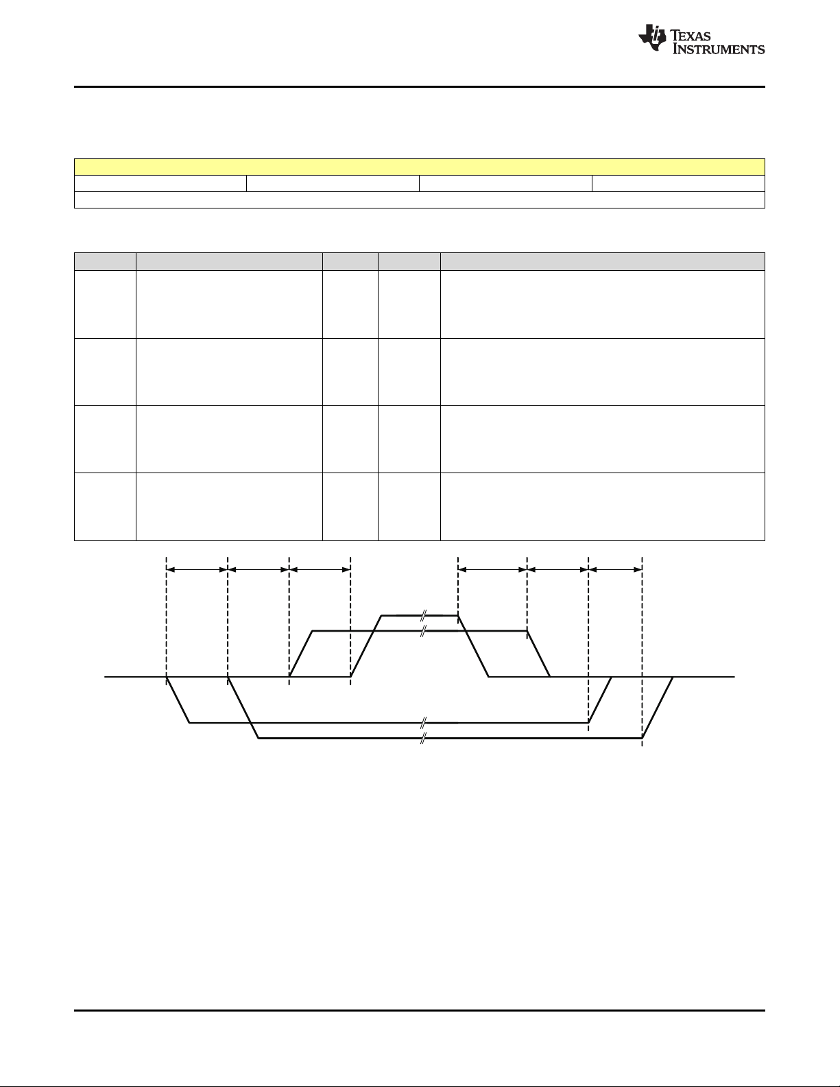
VNEG
VEE
VPOS
VDDH
6ms 6ms 48ms6ms 6ms 6ms
TPS65185, TPS651851
SLVSAQ8G –FEBRUARY 2011–REVISED SEPTEMBER 2017
8.6.10 Power-Up Sequence 0 (UPSEQ0) Register (address = 0x09h) [reset = E4h]
Figure 37. UPSEQ0 Register
7 6 5 4 3 2 1 0
VDDH_UP[1:0] VPOS_UP[1:0] VEE_UP[1:0] VNEG_UP[1:0]
R/W-3h R/W-2h R/W-1h R/W-0h
LEGEND: R/W = Read/Write; R = Read only; -n = value after reset
Table 12. UPSEQ0 Register Field Descriptions
Bit Field Type Reset Description
7-6 VDDH_UP R/W 3h VDDH power-up order
0h = Power up on STROBE1
1h = Power up on STROBE2
2h = Power up on STROBE3
3h = Power up on STROBE4
5-4 VPOS_UP R/W 2h VPOS power-up order
0h = Power up on STROBE1
1h = Power up on STROBE2
2h = Power up on STROBE3
3h = Power up on STROBE4
3-2 VEE_UP R/W 1h VEE power-up order
0h = Power up on STROBE1
1h = Power up on STROBE2
2h = Power up on STROBE3
3h = Power up on STROBE4
1-0 VNEG_UP R/W 0h VNEG power-up order
0h = Power up on STROBE1
1h = Power up on STROBE2
2h = Power up on STROBE3
3h = Power up on STROBE4
www.ti.com
42
Figure 38. Default Power-Up/Down Sequence
Submit Documentation Feedback Copyright © 2011–2017, Texas Instruments Incorporated
Product Folder Links: TPS65185

TPS65185, TPS651851
www.ti.com
SLVSAQ8G –FEBRUARY 2011–REVISED SEPTEMBER 2017
8.6.11 Power-Up Sequence 1 (UPSEQ1) Register (address = 0x0Ah) [reset = 55h]
Figure 39. UPSEQ1 Register
7 6 5 4 3 2 1 0
UDLY4[1:0] UDLY3[1:0] UDLY2[1:0] UDLY1[1:0]
R/W-1h R/W-1h R/W-1h R/W-1h
LEGEND: R/W = Read/Write; R = Read only; -n = value after reset
Table 13. UPSEQ1 Register Field Descriptions
Bit Field Type Reset Description
7-6 UDLY4 R/W 1h DLY4 delay time set; defines the delay time from STROBE3 to
5-4 UDLY3 R/W 1h DLY3 delay time set; defines the delay time from STROBE2 to
3-2 UDLY2 R/W 1h DLY2 delay time set; defines the delay time from STROBE1 to
1-0 UDLY1 R/W 1h DLY1 delay time set; defines the delay time from VN_PG high to
STROBE4 during power up.
0h = 3 ms
1h = 6 ms
2h = 9 ms
3h = 12 ms
STROBE3 during power up.
0h = 3 ms
1h = 6 ms
2h = 9 ms
3h = 12 ms
STROBE2 during power up.
0h = 3 ms
1h = 6 ms
2h = 9 ms
3h = 12 ms
STROBE1 during power up.
0h = 3 ms
1h = 6 ms
2h = 9 ms
3h = 12 ms
Product Folder Links: TPS65185
Submit Documentation FeedbackCopyright © 2011–2017, Texas Instruments Incorporated
43

TPS65185, TPS651851
SLVSAQ8G –FEBRUARY 2011–REVISED SEPTEMBER 2017
8.6.12 Power-Down Sequence 0 (DWNSEQ0) Register (address = 0x0Bh) [reset = 1Eh]
Figure 40. DWNSEQ0 Register
7 6 5 4 3 2 1 0
VDDH_DWN[1:0] VPOS_DWN[1:0] VEE_DWN[1:0] VNEG_DWN[1:0]
R/W-0h R/W-1h R/W-3h R/W-2h
LEGEND: R/W = Read/Write; R = Read only; -n = value after reset
Table 14. DWNSEQ0 Register Field Descriptions
Bit Field Type Reset Description
7-6 VDDH_DWN R/W 0h VDDH power-down order
0h = Power down on STROBE1
1h = Power down on STROBE2
2h = Power down on STROBE3
3h = Power down on STROBE4
5-4 VPOS_DWN R/W 1h VPOS power-down order
0h = Power down on STROBE1
1h = Power down on STROBE2
2h = Power down on STROBE3
3h = Power down on STROBE4
3-2 VEE_DWN R/W 3h VEE power-down order
0h = Power down on STROBE1
1h = Power down on STROBE2
2h = Power down on STROBE3
3h = Power down on STROBE4
1-0 VNEG_DWN R/W 2h VNEG power-down order
0h = Power down on STROBE1
1h = Power down on STROBE2
2h = Power down on STROBE3
3h = Power down on STROBE4
www.ti.com
44
Submit Documentation Feedback Copyright © 2011–2017, Texas Instruments Incorporated
Product Folder Links: TPS65185
TPS65185, TPS651851
www.ti.com
SLVSAQ8G –FEBRUARY 2011–REVISED SEPTEMBER 2017
8.6.13 Power-Down Sequence 1 (DWNSEQ1) Register (address = 0x0Ch) [reset = E0h]
Figure 41. DWNSEQ1 Register
7 6 5 4 3 2 1 0
DDLY4[1:0] DDLY3[1:0] DDLY2[1:0] DDLY1 DFCTR
R/W-3h R/W-2h R/W-0h R/W-0h R/W-0h
LEGEND: R/W = Read/Write; R = Read only; -n = value after reset
Table 15. DWNSEQ1 Register Field Descriptions
Bit Field Type Reset Description
7-6 DDLY4 R/W 3h DLY4 delay time set; defines the delay time from STROBE3 to
5-4 DDLY3 R/W 2h DLY3 delay time set; defines the delay time from STROBE2 to
3-2 DDLY2 R/W 0h DLY2 delay time set; defines the delay time from STROBE1 to
1 DDLY1 R/W 0h DLY2 delay time set; defines the delay time from WAKEUP low
0 DFCTR R/W 0h At power-down delay time DLY2[1:0], DLY3[1:0], DLY4[1:0] are
STROBE4 during power down.
0h = 6 ms
1h = 12 ms
2h = 24 ms
3h = 48 ms
STROBE3 during power down.
0h = 6 ms
1h = 12 ms
2h = 24 ms
3h = 48 ms
STROBE2 during power down.
0h = 6 ms
1h = 12 ms
2h = 24 ms
3h = 48 ms
to STROBE1 during power down.
0h = 3 ms
1h = 6 ms
multiplied with DFCTR[1:0]
0h = 1x
1h = 16x
Product Folder Links: TPS65185
Submit Documentation FeedbackCopyright © 2011–2017, Texas Instruments Incorporated
45
TPS65185, TPS651851
SLVSAQ8G –FEBRUARY 2011–REVISED SEPTEMBER 2017
8.6.14 Thermistor 1 (TMST1) Register (address = 0x0Dh) [reset = 20h]
Figure 42. TMST1 Register
7 6 5 4 3 2 1 0
READ_THERM Not used CONV_END Not used Not used Not used DT[1:0]
R/W-0h R/W-0h R-1h R/W-0h R/W-0h R/W-0h R/W-0h
LEGEND: R/W = Read/Write; R = Read only; -n = value after reset
Table 16. TMST1 Register Field Descriptions
Bit Field Type Reset Description
7 READ_THERM R/W 0h Read thermistor value
0h = No effect
1h = Initiates temperature acquisition
NOTE: Bit is self-cleared after acquisition is completed
6 Not used R/W 0h Not used
5 CONV_END R 1h ADC conversion done flag
0h = Conversion is not finished
1h = Conversion is finished
4 Not used R/W 0h Not used
3 Not used R/W 0h Not used
2 Not used R/W 0h Not used
1-0 DT R/W 0h Panel temperature-change interrupt threshold
0h = 2°C
1h = 3°C
2h = 4°C
3h = 5°C
DTX interrupt is issued when difference between most recent
temperature reading and baseline temperature is equal to or
greater than threshold value. See Hot, Cold, and Temperature-
Change Interrupts for details.
www.ti.com
46
Submit Documentation Feedback Copyright © 2011–2017, Texas Instruments Incorporated
Product Folder Links: TPS65185
TPS65185, TPS651851
www.ti.com
SLVSAQ8G –FEBRUARY 2011–REVISED SEPTEMBER 2017
8.6.15 Thermistor 2 (TMST2) Register (address = 0x0Eh) [reset = 78h]
Figure 43. TMST2 Register
7 6 5 4 3 2 1 0
TMST_COLD[3:0] TMST_HOT[3:0]
R/W-7h R/W-8h
LEGEND: R/W = Read/Write; R = Read only; -n = value after reset
Table 17. TMST2 Register Field Descriptions
Bit Field Type Reset Description
7-4 READ_THERM R/W 7h Thermistor COLD threshold
3-0 TMST_HOT R/W 8h Thermistor HOT threshold
0h = –7°C
1h = –6°C
2h = –5°C
3h = –4°C
4h = –3°C
5h = –2°C
6h = –1°C
7h = 0°C
8h = 1°C
9h = 2°C
Ah = 3°C
Bh = 4°C
Ch = 5°C
Dh = 6°C
Eh = 7°C
Fh = 8°C
NOTE: An interrupt is issued when thermistor temperature is
equal or less than COLD threshold
0h = 42°C
1h = 43°C
2h = 44°C
3h = 45°C
4h = 46°C
5h = 47°C
6h = 48°C
7h = 49°C
8h = 50°C
9h = 51°C
Ah = 52°C
Bh = 53°C
Ch = 54°C
Dh = 55°C
Eh = 56°C
Fh = 57°C
NOTE: An interrupt is issued when thermistor temperature is
equal or greater than HOT threshold
Product Folder Links: TPS65185
Submit Documentation FeedbackCopyright © 2011–2017, Texas Instruments Incorporated
47

TPS65185, TPS651851
SLVSAQ8G –FEBRUARY 2011–REVISED SEPTEMBER 2017
8.6.16 Power Good Status (PG) Register (address = 0x0Fh) [reset = 0h]
NOTE: PG pin is pulled hi (HiZ state) when VDDH_PG = VPOS_PG = VEE_PG = VNEG_PG = 1
Figure 44. PG Register
7 6 5 4 3 2 1 0
VB_PG VDDH_PG VN_PG VPOS_PG VEE_PG Not used VNEG_PG Not used
R-0h R-0h R-0h R-0h R-0h R-0h R-0h R-0h
LEGEND: R/W = Read/Write; R = Read only; -n = value after reset
Table 18. PG Register Field Descriptions
Bit Field Type Reset Description
7 VB_PG R 0h Positive boost converter power good
0h = DCDC1 is not in regulation or turned off
1h = DCDC1 is in regulation
6 VDDH_PG R 0h VDDH power good
0h = VDDH charge pump is not in regulation or turned off
1h = VDDH charge pump is in regulation
5 VN_PG R 0h Inverting buck-boost power good
0h = DCDC2 is not in regulation or turned off
1h = DCDC2 is in regulation
4 VPOS_PG R 0h VPOS power good
0h = LDO1(VPOS) is not in regulation or turned off
1h = LDO1(VPOS) is in regulation
3 VEE_PG R 0h VEE power good
0h = VEE charge pump is not in regulation or turned off
1h = VEE charge pump is in regulation
2 Not used R 0h Not used
1 VNEG_PG R 0h VNEG power good
0h = LDO2(VNEG) is not in regulation or turned off
1h = LDO2(VNEG) is in regulation
0 Not used R 0h Not used
www.ti.com
8.6.17 Revision and Version Control (REVID) Register (address = 0x10h) [reset = 45h] Figure 45. REVID Register
7 6 5 4 3 2 1 0
REVID[7:0]
R-45h
LEGEND: R/W = Read/Write; R = Read only; -n = value after reset
Table 19. REVID Register Field Descriptions
Bit Field Type Reset Description
7-0 REVID R 45h REVID[7:6] = MJREV
REVID[5:4] = MNREV
REVID[3:0] = VERSION
45h = TPS65185 1p0
55h = TPS65185 1p1
65h = TPS65185 1p2
66h = TPS651851 1p0
48
Submit Documentation Feedback Copyright © 2011–2017, Texas Instruments Incorporated
Product Folder Links: TPS65185

DCDC2
VIN_P
10µF
4.7 µF
VPOS
10nF 2.2 Fµ
1 MΩ
52.3 kΩ
VEE_D
VEE_DRV
VEE_FB
4.7 µH
VN_SW
From Battery
(3 V to 6 V)
VEE (–20 V)
VPOS (15 V)
DCDC1
4.7 Fµ
2.2 Hµ
PGND1
VB_SW
10 Fµ
10 nF2.2 Fµ
1 MΩ
47.5 kΩ
VDDH_D
VDDH_DRV
VDDH_FB
From Battery
(3 V to 6 V)
VDDH (22 V )
VDDH_EN VEE_EN
PGND2 PGND2
VPOS_EN
VB
LDO1
VEE
CHARGE
PUMP
VN
PBKG
PGND2
4.7 Fµ
VNEG_IN
VDDH_IN
VNEG
VNEG (–15 V)
VNEG_EN
LDO2
Thermal Pad
TEMP
SENSOR
43 kΩ
10k NTCΩ
TS
AGND2 ADC
TMST_VALUE[7:0]
4.7 Fµ
4.7 Fµ
VPOS_IN
VIN
10 Fµ
VCOM_PWR
4.7 Fµ
From Input Supply
(3 V to 6 V)
4.7 Fµ
VREF
AGND1
DAC
VCOM
VCOM[8:0]
VCOM_CTRL
4.7 Fµ
From Cµ
VREF
4.7 µF
INT_LDO
INT_LDO
VEE_IN
VDDH
CHARGE
PUMP
4.7 Fµ
3.3-V supply from system
To EPD panel
VIN3P3
V3P3
GATE DRIVER
V3P3_EN
1 kΩ
SCL
From µC
From/to µC or DSP
SDA
10 kΩ
VIO
PWR_GOOD
10 kΩ
VIO
DIGITAL
CORE
WAKEUP
INT
10 kΩ
VIO
10 kΩ
VIO
From Cµ
PWRUP
From Cµ
To µC
To µC
DGND
100 nF 100nF
To panel back-plane
(0 to to 5.11 V )
Copyright © 2017, Texas Instruments Incorporated
TPS65185, TPS651851
www.ti.com
SLVSAQ8G –FEBRUARY 2011–REVISED SEPTEMBER 2017
9 Application and Implementation
NOTE
Information in the following applications sections is not part of the TI component
specification, and TI does not warrant its accuracy or completeness. TI’s customers are
responsible for determining suitability of components for their purposes. Customers should
validate and test their design implementation to confirm system functionality.
9.1 Application Information
The TPS65185x device is used to power display screens in E-book applications, specifically E-Ink Vizplex
display, by connecting the screen to the positive and negative charge pump, LDO1, LDO2, and VCOM rails. The
device supports display screens up to 9.7 inches.
9.2 Typical Application
Figure 46. Typical Application Schematic
Product Folder Links: TPS65185
Submit Documentation FeedbackCopyright © 2011–2017, Texas Instruments Incorporated
49

TPS65185, TPS651851
SLVSAQ8G –FEBRUARY 2011–REVISED SEPTEMBER 2017
www.ti.com
Typical Application (continued)
9.2.1 Design Requirements
For this design example, use the parameters listed in Table 20 as the input parameters.
Table 20. Design Parameters
VOLTAGE SEQUENCE (STROBE)
VNEG (LDO2) –15 V 1
VEE (Charge pump 2) –20 V 2
VPOS (LDO1) 15 V 3
VDDH (Charge pump 1) 22 V 4
9.2.2 Detailed Design Procedure
For the positive boost regulator (DCDC1) a 10-μF capacitor can be used as the input capacitor value; two 4.7-μF
capacitors are used as output capacitors to reduce ESR along with a 2.2-μH inductor. For the inverting buckboost regulator (DCDC2), a 10-μF capacitor can be used at the input capacitor value; two 4.7-μF capacitors are
used as output capacitors to reduce ESR along with a 4.7-μH inductor. The charge pump pins VDDH_D and
VEE_D require 100-nF capacitors to ground for reliable operation. An ESR capacitor with a value of 20 mΩ is
expected for all capacitors, and ceramic X5R material or better is recommended. These values are the typical the
values used; additional inductor and capacitor values can be used for improved functionality; however, the
components should be rated the same as the recommended external components listed in Table 21.
Table 21. Recommended External Components
PART NUMBER VALUE SIZE MANUFACTURER
INDUCTORS
LQH44PN4R7MP0 4.7 µH 4 mm × 4 mm × 1.65 mm Murata
NR4018T4R7M 4.7 µH 4 mm × 4 mm × 1.8 mm Taiyo Yuden
VLS252015ET-2R2M 2.2 µH 2 mm × 2.5 mm × 1.5 mm TDK
NR4012T2R2M 2.2 µH 4 mm × 4 mm × 1.2 mm Taiyo Yuden
CAPACITORS
GRM21BC81E475KA12L 4.7 µF, 25 V, X6S 805 Murata
GRM32ER71H475KA88L 4.7 µF, 50 V, X7R 1210 Murata
All other capacitors X5R or better — —
DIODES
BAS3010 — SOD-323 Infineon
MBR130T1 — SOD-123 ON-Semi
BAV99 — SOT-23 Fairchild
THERMISTOR
NCP18XH103F03RB 10 kΩ 603 Murata
50
Submit Documentation Feedback Copyright © 2011–2017, Texas Instruments Incorporated
Product Folder Links: TPS65185
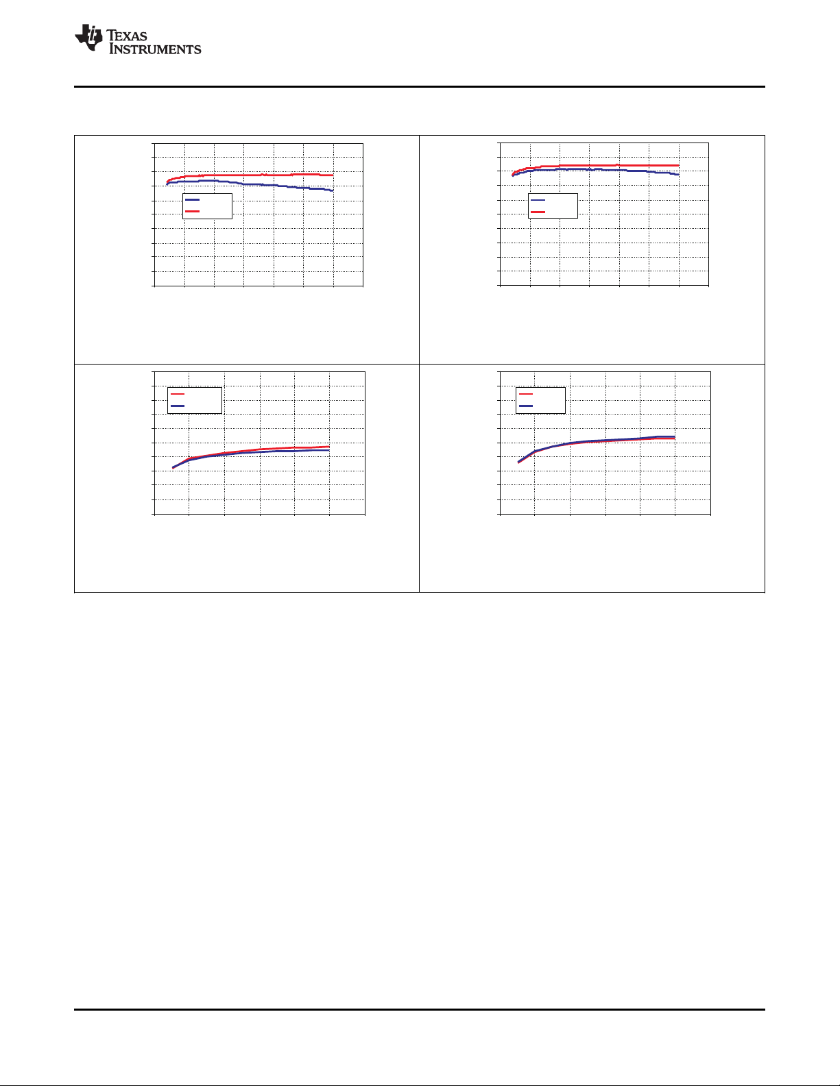
0
10
20
30
40
50
60
70
80
90
100
0 2 4 6 8 10 12
Output C urrent [mA ]
Efficiency [%]
VIN=5 V
VIN=3 .5V
0
10
20
30
40
50
60
70
80
90
100
0 2 4 6 8 10 12
Output C urrent [mA ]
Efficiency [%]
VIN= 5V
VIN= 3.5
0
10
20
30
40
50
60
70
80
90
100
0 25 50 7 5 100 1 25 150 175
Outpu t Curre nt [m A]
Efficiency [%]
VIN= 3. 5
VIN= 5V
0
10
20
30
40
50
60
70
80
90
100
0 25 50 7 5 100 125 150 175
Output C urrent [m A]
Efficiency [% ]
VIN= 3.5
VIN= 5V
www.ti.com
9.2.3 Application Curves
TPS65185, TPS651851
SLVSAQ8G –FEBRUARY 2011–REVISED SEPTEMBER 2017
T = 25°C
Figure 47. VN DCDC Efficiency
T = 25°C
Figure 49. VEE Charge Pump Efficiency
T = 25°C
Figure 48. VB DCDC Efficiency
T = 25°C
Figure 50. VDDH Charge Pump Efficiency
10 Power Supply Recommendations
The device is designed to operate with an input voltage supply range from 3 V to 6 V, where Figure 5 and
Figure 6 show how lower input supply voltages can result in larger inrush currents. This input supply can be from
a externally regulated supply. If the input supply is located more than a few inches from the TPS65185x,
additional bulk capacitance may be required in addition to the ceramic bypass capacitors. An electrolytic
capacitor with a value of 10 µF is a typical choice.
Product Folder Links: TPS65185
Submit Documentation FeedbackCopyright © 2011–2017, Texas Instruments Incorporated
51

TPS6518x
Thermal Pad
Bottom Layer
VN Connection
TPS65185, TPS651851
SLVSAQ8G –FEBRUARY 2011–REVISED SEPTEMBER 2017
www.ti.com
11 Layout
11.1 Layout Guidelines
1. PBKG (Die substrate) must connect to VN (–16 V) with short, wide trace. Wide copper trace will improve
heat dissipation.
2. The thermal pad is internally connected to PBKG and must not be connected to ground, but connected to VN
with a short wide copper trace.
3. Inductor traces must be kept on the PCB top layer free of any vias.
4. Feedback traces must be routed away from any potential noise source to avoid coupling.
5. Output caps must be placed immediately at output pin.
6. The VIN pins must be bypassed to ground with low ESR ceramic bypass capacitors.
11.2 Layout Example
52
Figure 51. Layout Diagram
Submit Documentation Feedback Copyright © 2011–2017, Texas Instruments Incorporated
Product Folder Links: TPS65185

TPS65185, TPS651851
www.ti.com
SLVSAQ8G –FEBRUARY 2011–REVISED SEPTEMBER 2017
12 Device and Documentation Support
12.1 Device Support
12.1.1 Third-Party Products Disclaimer
TI'S PUBLICATION OF INFORMATION REGARDING THIRD-PARTY PRODUCTS OR SERVICES DOES NOT
CONSTITUTE AN ENDORSEMENT REGARDING THE SUITABILITY OF SUCH PRODUCTS OR SERVICES
OR A WARRANTY, REPRESENTATION OR ENDORSEMENT OF SUCH PRODUCTS OR SERVICES, EITHER
ALONE OR IN COMBINATION WITH ANY TI PRODUCT OR SERVICE.
12.2 Documentation Support
12.2.1 Related Documentation
For related documentation see the following:
• Texas Instruments, TPS65185 Evaluation Module user's guide
• Texas Instruments, Understanding Undervoltage Lockout in Display Power Devices application report
12.3 Receiving Notification of Documentation Updates
To receive notification of documentation updates, navigate to the device product folder on ti.com. In the upper
right corner, click on Alert me to register and receive a weekly digest of any product information that has
changed. For change details, review the revision history included in any revised document.
12.4 Community Resources
The following links connect to TI community resources. Linked contents are provided "AS IS" by the respective
contributors. They do not constitute TI specifications and do not necessarily reflect TI's views; see TI's Terms of
Use.
TI E2E™ Online Community TI's Engineer-to-Engineer (E2E) Community. Created to foster collaboration
among engineers. At e2e.ti.com, you can ask questions, share knowledge, explore ideas and help
solve problems with fellow engineers.
Design Support TI's Design Support Quickly find helpful E2E forums along with design support tools and
contact information for technical support.
12.5 Trademarks
OMAP, E2E are trademarks of Texas Instruments.
Vizplex is a trademark of E Ink Corporation.
E Ink is a registered trademark of E Ink Corporation.
All other trademarks are the property of their respective owners.
12.6 Electrostatic Discharge Caution
This integrated circuit can be damaged by ESD. Texas Instruments recommends that all integrated circuits be handled with
appropriate precautions. Failure to observe proper handling and installation procedures can cause damage.
ESD damage can range from subtle performance degradation to complete device failure. Precision integrated circuits may be more
susceptible to damage because very small parametric changes could cause the device not to meet its published specifications.
12.7 Glossary
SLYZ022 — TI Glossary.
This glossary lists and explains terms, acronyms, and definitions.
13 Mechanical, Packaging, and Orderable Information
The following pages include mechanical, packaging, and orderable information. This information is the most
current data available for the designated devices. This data is subject to change without notice and revision of
this document. For browser-based versions of this data sheet, refer to the left-hand navigation.
Submit Documentation FeedbackCopyright © 2011–2017, Texas Instruments Incorporated
Product Folder Links: TPS65185
53
PACKAGE OPTION ADDENDUM
www.ti.com
10-Dec-2020
PACKAGING INFORMATION
Orderable Device Status
TPS651851RSLR ACTIVE VQFN RSL 48 2500 RoHS & Green NIPDAU Level-3-260C-168 HR -10 to 85 TPS
TPS651851RSLT ACTIVE VQFN RSL 48 250 RoHS & Green NIPDAU Level-3-260C-168 HR -10 to 85 TPS
TPS65185RGZR ACTIVE VQFN RGZ 48 2500 RoHS & Green NIPDAU Level-3-260C-168 HR -40 to 85 E INK
TPS65185RGZT ACTIVE VQFN RGZ 48 250 RoHS & Green NIPDAU Level-3-260C-168 HR -40 to 85 E INK
TPS65185RSLR ACTIVE VQFN RSL 48 2500 RoHS & Green NIPDAU Level-3-260C-168 HR -40 to 85 TPS
TPS65185RSLT ACTIVE VQFN RSL 48 250 RoHS & Green NIPDAU Level-3-260C-168 HR -40 to 85 TPS
(1)
The marketing status values are defined as follows:
ACTIVE: Product device recommended for new designs.
LIFEBUY: TI has announced that the device will be discontinued, and a lifetime-buy period is in effect.
NRND: Not recommended for new designs. Device is in production to support existing customers, but TI does not recommend using this part in a new design.
PREVIEW: Device has been announced but is not in production. Samples may or may not be available.
OBSOLETE: TI has discontinued the production of the device.
Package Type Package
(1)
Drawing
Pins Package
Qty
Eco Plan
(2)
Lead finish/
Ball material
(6)
MSL Peak Temp
(3)
Op Temp (°C) Device Marking
(4/5)
651851
651851
TPS65185
TPS65185
65185
65185
(2)
RoHS: TI defines "RoHS" to mean semiconductor products that are compliant with the current EU RoHS requirements for all 10 RoHS substances, including the requirement that RoHS substance
do not exceed 0.1% by weight in homogeneous materials. Where designed to be soldered at high temperatures, "RoHS" products are suitable for use in specified lead-free processes. TI may
reference these types of products as "Pb-Free".
RoHS Exempt: TI defines "RoHS Exempt" to mean products that contain lead but are compliant with EU RoHS pursuant to a specific EU RoHS exemption.
Green: TI defines "Green" to mean the content of Chlorine (Cl) and Bromine (Br) based flame retardants meet JS709B low halogen requirements of <=1000ppm threshold. Antimony trioxide based
flame retardants must also meet the <=1000ppm threshold requirement.
(3)
MSL, Peak Temp. - The Moisture Sensitivity Level rating according to the JEDEC industry standard classifications, and peak solder temperature.
(4)
There may be additional marking, which relates to the logo, the lot trace code information, or the environmental category on the device.
(5)
Multiple Device Markings will be inside parentheses. Only one Device Marking contained in parentheses and separated by a "~" will appear on a device. If a line is indented then it is a continuation
of the previous line and the two combined represent the entire Device Marking for that device.
Samples
Addendum-Page 1

PACKAGE OPTION ADDENDUM
www.ti.com
(6)
Lead finish/Ball material - Orderable Devices may have multiple material finish options. Finish options are separated by a vertical ruled line. Lead finish/Ball material values may wrap to two
lines if the finish value exceeds the maximum column width.
10-Dec-2020
Important Information and Disclaimer:The information provided on this page represents TI's knowledge and belief as of the date that it is provided. TI bases its knowledge and belief on information
provided by third parties, and makes no representation or warranty as to the accuracy of such information. Efforts are underway to better integrate information from third parties. TI has taken and
continues to take reasonable steps to provide representative and accurate information but may not have conducted destructive testing or chemical analysis on incoming materials and chemicals.
TI and TI suppliers consider certain information to be proprietary, and thus CAS numbers and other limited information may not be available for release.
In no event shall TI's liability arising out of such information exceed the total purchase price of the TI part(s) at issue in this document sold by TI to Customer on an annual basis.
Addendum-Page 2
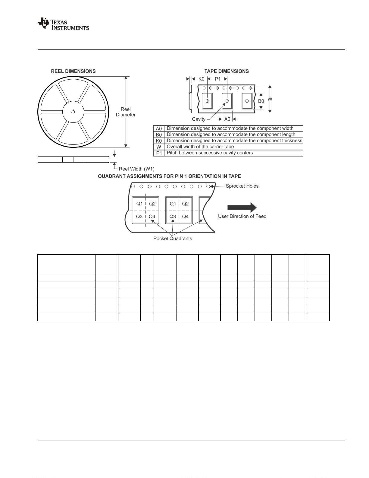
PACKAGE MATERIALS INFORMATION
www.ti.com 12-Sep-2017
TAPE AND REEL INFORMATION
*All dimensions are nominal
Device Package
TPS651851RSLR VQFN RSL 48 2500 330.0 16.4 6.3 6.3 1.1 12.0 16.0 Q2
TPS651851RSLT VQFN RSL 48 250 180.0 16.4 6.3 6.3 1.1 12.0 16.0 Q2
TPS65185RGZR VQFN RGZ 48 2500 330.0 16.4 7.3 7.3 1.1 12.0 16.0 Q2
TPS65185RGZT VQFN RGZ 48 250 180.0 16.4 7.3 7.3 1.1 12.0 16.0 Q2
TPS65185RSLR VQFN RSL 48 2500 330.0 16.4 6.3 6.3 1.1 12.0 16.0 Q2
TPS65185RSLT VQFN RSL 48 250 180.0 16.4 6.3 6.3 1.1 12.0 16.0 Q2
Type
Package
Drawing
Pins SPQ Reel
Diameter
(mm)
Reel
Width
W1 (mm)
A0
(mm)B0(mm)K0(mm)P1(mm)W(mm)
Pin1
Quadrant
Pack Materials-Page 1
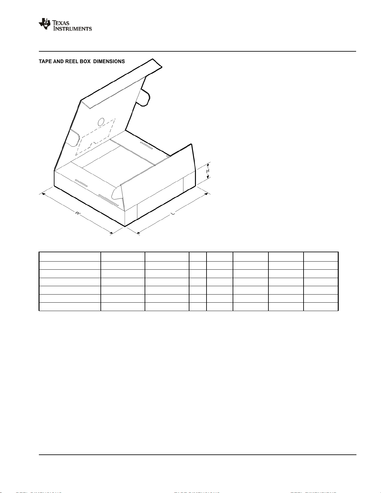
PACKAGE MATERIALS INFORMATION
www.ti.com 12-Sep-2017
*All dimensions are nominal
Device Package Type Package Drawing Pins SPQ Length (mm) Width (mm) Height (mm)
TPS651851RSLR VQFN RSL 48 2500 367.0 367.0 38.0
TPS651851RSLT VQFN RSL 48 250 210.0 185.0 35.0
TPS65185RGZR VQFN RGZ 48 2500 367.0 367.0 38.0
TPS65185RGZT VQFN RGZ 48 250 210.0 185.0 35.0
TPS65185RSLR VQFN RSL 48 2500 367.0 367.0 38.0
TPS65185RSLT VQFN RSL 48 250 210.0 185.0 35.0
Pack Materials-Page 2

GENERIC PACKAGE VIEW
VQFN - 1 mm max heightRGZ 48
7 x 7, 0.5 mm pitch
PLASTIC QUADFLAT PACK- NO LEAD
Images above are just a representation of the package family, actual package may vary.
Refer to the product data sheet for package details.
www.ti.com
4224671/A
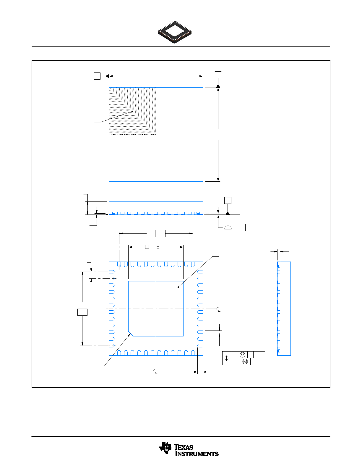
PACKAGE OUTLINE
PIN 1 INDEX AREA
1 MAX
SCALE 2.000
B
7.15
6.85
A
7.15
6.85
VQFN - 1 mm max heightRGZ0048B
PLASTIC QUAD FLATPACK - NO LEAD
C
SEATING PLANE
0.05
0.00
44X 0.5
2X
5.5
PIN 1 ID
(OPTIONAL)
12
2X 5.5
4.1 0.1
13
49
1
48
SYMM
48X
24
25
SYMM
36
37
0.5
0.3
0.08 C
EXPOSED
THERMAL PAD
0.30
48X
0.18
0.1 C B A
0.05
(0.2) TYP
4218795/B 02/2017
NOTES:
1. All linear dimensions are in millimeters. Any dimensions in parenthesis are for reference only. Dimensioning and tolerancing
per ASME Y14.5M.
2. This drawing is subject to change without notice.
3. The package thermal pad must be soldered to the printed circuit board for thermal and mechanical performance.
www.ti.com
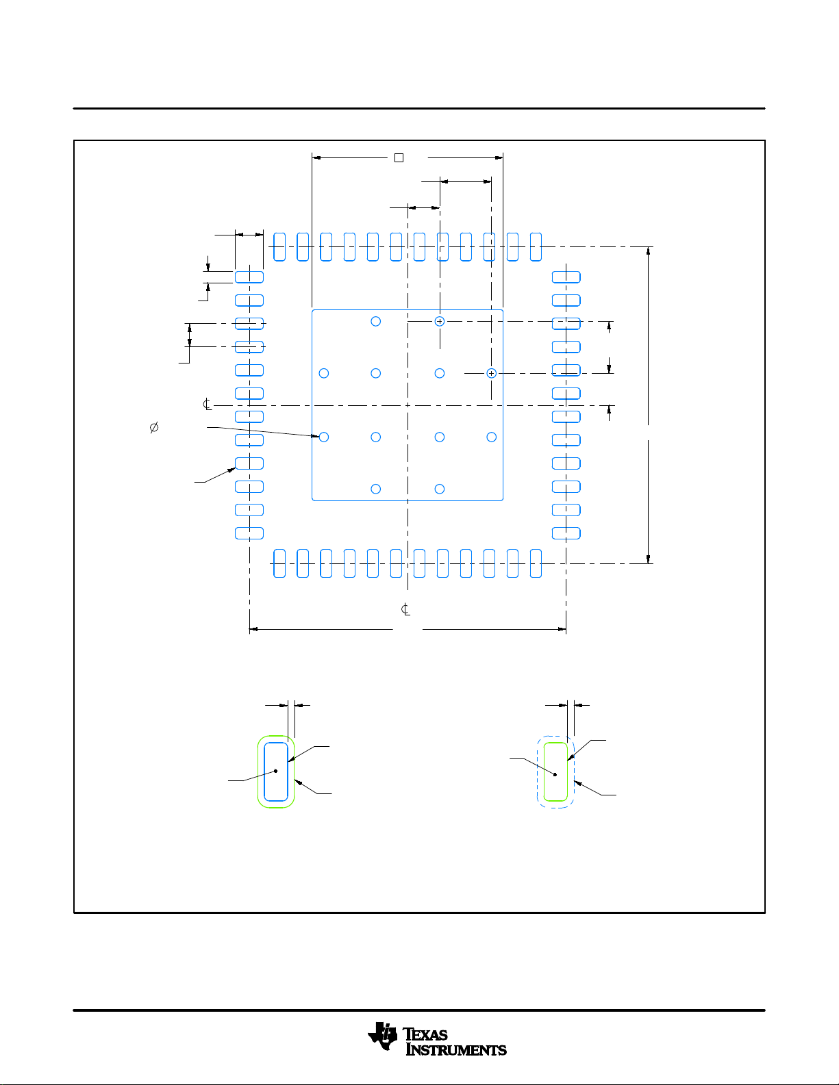
48X (0.24)
44X (0.5)
48X (0.6)
SYMM
EXAMPLE BOARD LAYOUT
VQFN - 1 mm max heightRGZ0048B
PLASTIC QUAD FLATPACK - NO LEAD
( 4.1)
(1.115) TYP
(0.685)
48
1
TYP
49
37
36
(1.115)
TYP
(0.685)
TYP
( 0.2) TYP
VIA
(R0.05)
TYP
0.07 MAX
ALL AROUND
EXPOSED METAL
12
13
SYMM
(6.8)
LAND PATTERN EXAMPLE
EXPOSED METAL SHOWN
SCALE:12X
ALL AROUND
METAL
EXPOSED METAL
SOLDER MASK
OPENING
(6.8)
25
24
0.07 MIN
SOLDER MASK
OPENING
METAL UNDER
SOLDER MASK
NON SOLDER MASK
DEFINED
(PREFERRED)
SOLDER MASK
DEFINED
SOLDER MASK DETAILS
4218795/B 02/2017
NOTES: (continued)
4. This package is designed to be soldered to a thermal pad on the board. For more information, see Texas Instruments literature
number SLUA271 (www.ti.com/lit/slua271).
5. Vias are optional depending on application, refer to device data sheet. If any vias are implemented, refer to their locations shown
on this view. It is recommended that vias under paste be filled, plugged or tented.
www.ti.com
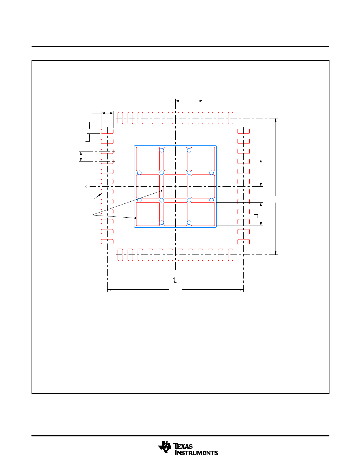
48X (0.6)
48X (0.24)
EXAMPLE STENCIL DESIGN
VQFN - 1 mm max heightRGZ0048B
PLASTIC QUAD FLATPACK - NO LEAD
(1.37)
48
1
TYP
37
36
44X (0.5)
(R0.05) TYP
METAL
TYP
SYMM
49
12
13
SYMM
(6.8)
SOLDER PASTE EXAMPLE
BASED ON 0.125 mm THICK STENCIL
EXPOSED PAD 49
73% PRINTED SOLDER COVERAGE BY AREA UNDER PACKAGE
SCALE:12X
24
(1.37)
(
25
TYP
(6.8)
9X
1.17)
4218795/B 02/2017
NOTES: (continued)
6. Laser cutting apertures with trapezoidal walls and rounded corners may offer better paste release. IPC-7525 may have alternate
design recommendations.
www.ti.com


IMPORTANT NOTICE AND DISCLAIMER
TI PROVIDES TECHNICAL AND RELIABILITY DATA (INCLUDING DATASHEETS), DESIGN RESOURCES (INCLUDING REFERENCE
DESIGNS), APPLICATION OR OTHER DESIGN ADVICE, WEB TOOLS, SAFETY INFORMATION, AND OTHER RESOURCES “AS IS”
AND WITH ALL FAULTS, AND DISCLAIMS ALL WARRANTIES, EXPRESS AND IMPLIED, INCLUDING WITHOUT LIMITATION ANY
IMPLIED WARRANTIES OF MERCHANTABILITY, FITNESS FOR A PARTICULAR PURPOSE OR NON-INFRINGEMENT OF THIRD
PARTY INTELLECTUAL PROPERTY RIGHTS.
These resources are intended for skilled developers designing with TI products. You are solely responsible for (1) selecting the appropriate
TI products for your application, (2) designing, validating and testing your application, and (3) ensuring your application meets applicable
standards, and any other safety, security, or other requirements. These resources are subject to change without notice. TI grants you
permission to use these resources only for development of an application that uses the TI products described in the resource. Other
reproduction and display of these resources is prohibited. No license is granted to any other TI intellectual property right or to any third
party intellectual property right. TI disclaims responsibility for, and you will fully indemnify TI and its representatives against, any claims,
damages, costs, losses, and liabilities arising out of your use of these resources.
TI’s products are provided subject to TI’s Terms of Sale (www.ti.com/legal/termsofsale.html) or other applicable terms available either on
ti.com or provided in conjunction with such TI products. TI’s provision of these resources does not expand or otherwise alter TI’s applicable
warranties or warranty disclaimers for TI products.
Mailing Address: Texas Instruments, Post Office Box 655303, Dallas, Texas 75265
Copyright © 2020, Texas Instruments Incorporated
 Loading...