

Page 1
COMPGND
VIN
EN
IN
VREF
FB
OUT
PS_GND
SW
PowerPAD
C4
VIN
VOUT
C2
R2
R3
D1
L1 C5
C6
TPS63700
R1
C1
0.22 mF
22 mF
4.7 mH
0.1 mF
10 mF
2.7 V To 5.5 V
4.7 nF
−5 V
TPS63700
www.ti.com
1
FEATURES
2
• Adjustable Output Voltage Down to – 15 V
• 2.7-V to 5.5-V Input Voltage Range
• Up to 360-mA Output Current
• 1000-mA Typical Switch Current Limit
• Up to 84% Efficiency
• Typical 1.4-MHz Fixed-Frequency PWM
Operation
• Thermal Shutdown
• Typical – 19 V Output Overvoltage Protection
• 1.5- µ A Shutdown Current
• Small 3-mm × 3-mm SON-10 Package (DRC)
APPLICATIONS
• Generic Negative Voltage Supply
• Small-to-Medium Size OLED Displays
• PDAs, Pocket PCs, Smartphones
• Bias Supply
SLVS530B – SEPTEMBER 2005 – REVISED NOVEMBER 2007
DC-DC INVERTER
DESCRIPTION
The TPS63700 is an inverting dc-dc converter
generating a negative output voltage down to – 15 V
with output currents up to 360-mA, depending on
input-voltage to output-voltage ratio. With a total
efficiency up to 84%, the device is ideal for portable
battery-powered equipment. The input voltage range
of 2.7-V to 5.5-V allows the TPS63700 to be directly
powered from a Li-ion battery, from 3-cell NiMH/NiCd,
from a 3.3-V or 5-V supply rail. The TPS63700 comes
in a small 3-mm × 3-mm SON-10 package.
Furthermore, the high switching frequency of typically
1.4 MHz allows the use of small external
components. This, and the small package make a
small power supply solution possible.
The inverter operates with a fixed-frequency PWM
control topology. The device has an internal current
limit, overvoltage protection, and a thermal shutdown
for highest reliability under fault conditions.
1
2 PowerPAD is a trademark of Texas Instruments.
PRODUCTION DATA information is current as of publication date.
Products conform to specifications per the terms of the Texas
Instruments standard warranty. Production processing does not
necessarily include testing of all parameters.
Please be aware that an important notice concerning availability, standard warranty, and use in critical applications of
Texas Instruments semiconductor products and disclaimers thereto appears at the end of this data sheet.
Copyright © 2005 – 2007, Texas Instruments Incorporated
Page 2
www.ti.com
TPS63700
SLVS530B – SEPTEMBER 2005 – REVISED NOVEMBER 2007
This integrated circuit can be damaged by ESD. Texas Instruments recommends that all integrated circuits be handled with
appropriate precautions. Failure to observe proper handling and installation procedures can cause damage.
ESD damage can range from subtle performance degradation to complete device failure. Precision integrated circuits may be more
susceptible to damage because very small parametric changes could cause the device not to meet its published specifications.
ORDERING INFORMATION
T
A
SWITCH CURRENT LIMIT PACKAGE TYPE SYMBOL PART NUMBER
(1)
(2)
– 40 ° C to 85 ° C 1000 mA SON-10 NUB TPS63700DRC
(1) For the most current package and ordering information, see the Package Option Addendum at the end of this document, or see the TI
Web site at www.ti.com.
(2) The DRC package is available taped and reeled. Add an R suffix to the device type (i.e., TPS63700DRCR) to order quantities of 3000
devices per reel. Add a T suffix to the device type (i.e., TPS63700DRCT) to order quantities of 250 devices peer reel.
ABSOLUTE MAXIMUM RATINGS
over operating free-air temperature range unless otherwise noted
Input voltage range at VIN
Input voltage range at IN
Minimum voltage at VOUT
Voltage at EN, FB, COMP, PS
Differential voltage between OUT to V
Operating virtual junction temperature, T
Storage temperature range, T
(1) Stresses beyond those listed under "absolute maximum ratings ” may cause permanent damage to the device. These are stress ratings
only, and functional operation of the device at these or any other conditions beyond those indicated under "recommended operating
conditions ” is not implied. Exposure to absolute-maximum-rated conditions for extended periods may affect device reliability.
(2) All voltage values are with respect to network ground terminal, unless otherwise noted.
(2)
(2)
(2)
(2)
(2)
IN
J
STG
(1)
TPS63700
– 0.3 V to +6.0 V
VIN
– 18 V
– 0.3 V to VIN+ 0.3 V
24 V
– 40 ° C to 150 ° C
– 65 ° C to 150 ° C
PACKAGE
POWER RATING ABOVE TA= 25 ° C POWER RATING POWER RATING
DRC 2053 mW 21 mW/ ° C 1130 mW 821 mW
(1) The thermal resistance junction to ambient of the 10-pin DRC is Θ
maximum junction temperature forces the device into thermal shutdown.
RECOMMENDED OPERATING CONDITIONS
Input voltage range, V
Operating free-air temperature range, T
Operating virtual junction temperature range, T
I
A
DISSIPATION RATINGS TABLE
(1)
TA≤ 25 ° C DERATING FACTOR TA= 70 ° C TA= 85 ° C
= 48.7 ° C/W. Exceeding the
JA
MIN NOM MAX UNIT
2.7 5.5 V
– 40 85 ° C
J
– 40 125 ° C
2 Submit Documentation Feedback Copyright © 2005 – 2007, Texas Instruments Incorporated
Product Folder Link(s): TPS63700
Page 3
www.ti.com
TPS63700
SLVS530B – SEPTEMBER 2005 – REVISED NOVEMBER 2007
ELECTRICAL CHARACTERISTICS
– 40 ° C to 85 ° C, over recommended input voltage range, typical at an ambient temperature of 25 ° C (unless otherwise noted)
PARAMETER TEST CONDITIONS MIN TYP MAX UNIT
DC-DC STAGE
V
OUT
V
IN
V
REF
I
FB
V
FB
V
OUT
V
OVP
R
DS(ON)
I
LIM
D
MAX
D
MIN
CONTROL STAGE
f
S
V
EN
V
EN
I
EN
I
(Q)
I
SD
UVLO 2.1 2.35 2.7 V
Adjustable output
voltage range
– 15 – 2 V
Input voltage range PIN VIN, IN 2.7 5.5 V
Reference voltage I
Negative feedback input bias
current
Negative feedback
regulation voltage
= 10 µ A 1.2 1.213 1.225 V
REF
V
= 0.1 V
FBN
REF
2 nA
VIN= 2.7 V to 5.5 V – 0.024 0 0.024 V
DC output accuracy PWM mode, device switching, ± 3 %
Output overvoltage
protection
Inverter switch on-resistance m Ω
VIN= 3.6 V 440 600
VIN= 5 V 370 500
– 19 V
Inverter switch current limit 2.7 V < VIN< 5.5 V 860 1000 1140 mA
Maximum duty cycle
inverting converter
Minimum duty cycle
inverting converter
87.5%
12.5%
Oscillator frequency 1250 1380 1500 kHz
High level input voltage 1.4 V
Low level input voltage 0.4 V
Input current EN = VINor GND 0.01 0.1 µ A
Quiescent
current
VIN VIN= 3.6 V, I
IN 640 750 µ A
EN = VIN, no switching
V
OUT
= – 5 V
= 0, 330 400 µ A
OUT
Shutdown supply current EN = GND 0.2 1.5 µ A
Undervoltage lockout
threshold
Thermal shutdown 150 ° C
Thermal shutdown
hysteresis
Junction temperature decreasing 5 ° C
Copyright © 2005 – 2007, Texas Instruments Incorporated Submit Documentation Feedback 3
Product Folder Link(s): TPS63700
Page 4
www.ti.com
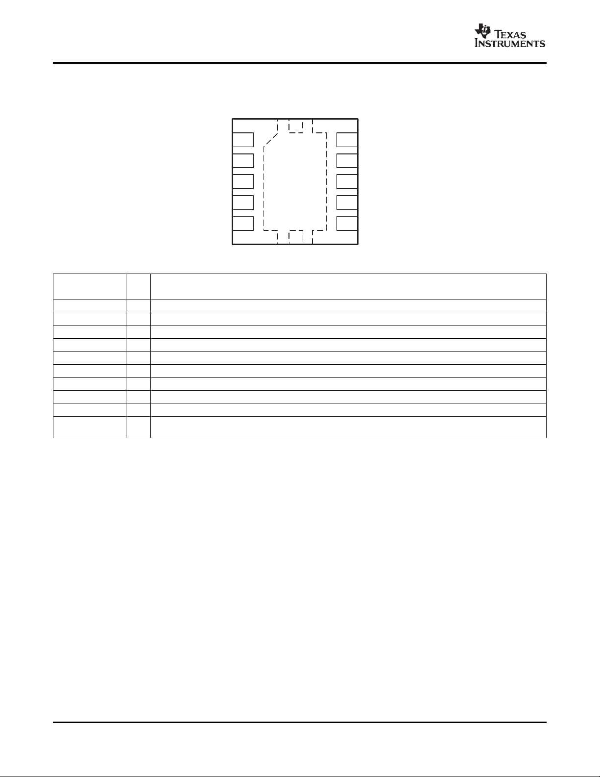
COMP 1
GND 2
VIN 3
EN 4
IN 5 SW6
PS_GND7
OUT8
FB9
VREF10
PowerPAD
TPS63700
SLVS530B – SEPTEMBER 2005 – REVISED NOVEMBER 2007
PIN ASSIGNMENTS
DRC PACKAGE PowerPAD™
(TOP VIEW)
Terminal Functions
TERMINAL
NAME NO.
COMP 1 I/O Compensation pin for control, connect a 4.7nF capacitor between this pin and GND
EN 4 I Enable pin (EN=GND: disabled; EN=VIN: enabled)
FB 9 I Feedback pin for the voltage divider
GND 2 Ground pin
IN 5 I supply voltage for the power switch
OUT 8 I Output voltage sense input
PS_GND 7 I Connect to GND for control logic
SW 6 O Inverter switch output
VIN 3 I supply voltage input for control logic, connect a RC circuit of 10R and 100nF to filter this supply voltage
VREF 10 O Reference voltage output. Connect a 220-nF capacitor to ground. Connect the lower resistor of the negative
I/O DESCRIPTION
output voltage divider to this pin.
4 Submit Documentation Feedback Copyright © 2005 – 2007, Texas Instruments Incorporated
Product Folder Link(s): TPS63700
Page 5
www.ti.com
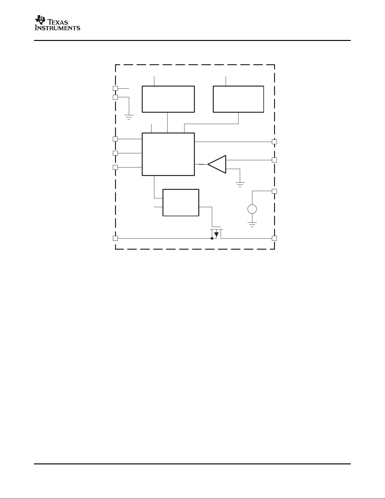
Gate
Control
Control Logic
Oscillator
Temperature
Control
+
−
−
+
VIN
GND
PS_GND
EN
COMP
IN
SW
VREF
FB
OUT
IN
VIN
VIN VIN
FUNCTIONAL BLOCK DIAGRAM
TPS63700
SLVS530B – SEPTEMBER 2005 – REVISED NOVEMBER 2007
Copyright © 2005 – 2007, Texas Instruments Incorporated Submit Documentation Feedback 5
Product Folder Link(s): TPS63700
Page 6
www.ti.com
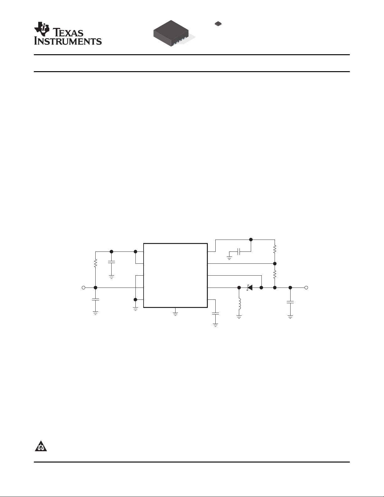
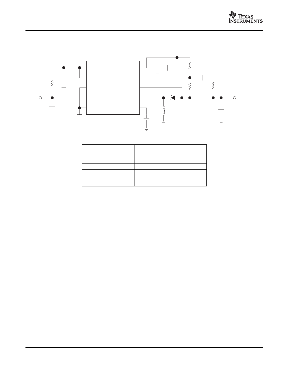
COMPGND
VIN
EN
IN
VREF
FB
OUT
PS_GND
SW
PowerPAD
C4
VIN
VOUT, −5 V
C2
R2
R3
C3
R4
D1
L1
C5
C6
TPS63700
C1
SL02/SL03
4x4.7 mF
0.22 mF
10 mF
10 pF
100 kW
4.7 nF
10 W
0.1 mF
TPS63700
SLVS530B – SEPTEMBER 2005 – REVISED NOVEMBER 2007
PARAMETER MEASUREMENT INFORMATION
REFERENCE DESCRIPTION
C1, C2, C3, C4, X7R/X5R ceramic
TYPICAL CHARACTERISTICS
List of Components
C5 4 × 4.7 µ F X7R/X5R ceramic
D1 SL03/SL02 Vishay
– 5V: TDK VLF4012 4R7, TDK
L1
SLF6025-4R7, Coilcraft LPS4018-472,
– 12V: Sumida CDRH5D18 10 µ H
6 Submit Documentation Feedback Copyright © 2005 – 2007, Texas Instruments Incorporated
Product Folder Link(s): TPS63700
Page 7
www.ti.com
0
10
20
30
40
50
60
70
80
90
0
100 200 300 400
Efficiency %
IO − Output Current − mA
VIN = 3.3 V
VIN = 5 V
VIN = 4.2 V
VIN = 3.6 V
V
OUT
= −5 V
0
50
100
150
200
250
300
350
400
2.5 3 3.5 4 4.5 5 5.5
Maximum Output Current − mA
VI − Input Voltage − V
VO = −5 V
VO = −12 V
VO = −15 V
SLVS530B – SEPTEMBER 2005 – REVISED NOVEMBER 2007
Table of Graphs
GRAPH DESCRIPTION
Figure 1 Maximum output current versus input voltage, V
Figure 2 Efficiency versus output current, V
Figure 3 Efficiency versus output current, V
Figure 4 Efficiency versus output current, V
Figure 5 Efficiency versus input voltage, V
Figure 6 Efficiency versus input voltage, V
Figure 7 Output voltage versus output current, V
Figure 8 Output voltage versus output current, V
= – 5 V
OUT
= – 12 V
OUT
= – 15V
OUT
= – 5 V
OUT
= – 12 V
OUT
OUT
OUT
= – 5 V
= – 12 V
= – 5 V, – 12 V, – 15 V
OUT
Figure 9 Output voltage in discontinuous conduction mode, VIN= 3.6 V, V
Figure 10 Output voltage in continuous conduction mode, VIN= 3.6 V, V
Figure 11 Load transient response, VIN= 3.6 V, V
Figure 12 Line transient response, VIN= 3.6 V to 4.2 V, V
Figure 13 Start-up after enable,V
= 3.6 V, V
I
OUT
= – 5 V, 45 to 150 mA
OUT
= – 5 V
= – 5 V
OUT
PERFORMANCE GRAPHS
TPS63700
= – 5 V
OUT
= – 5 V
OUT
MAXIMUM OUTPUT CURRENT vs
vs OUTPUT CURRENT,
INPUT VOLTAGE VOUT – 5V
Figure 1. Figure 2.
EFFICIENCY
Copyright © 2005 – 2007, Texas Instruments Incorporated Submit Documentation Feedback 7
Product Folder Link(s): TPS63700
Page 8
www.ti.com
0
10
20
30
40
50
60
70
80
90
0 20 40 60 80 100 120 140 160 180 200
Efficiency %
IO − Output Current − mA
VIN = 5 V
V
OUT
= −15 V
VIN = 4.2 V
VIN = 3.3 V
0
10
20
30
40
50
60
70
80
90
0 50
100 150
200 250
VIN = 4.2 V
VIN = 5 V
VIN = 3.6 V
VIN = 3.3 V
IO − Output Current − mA
V
OUT
= −12 V
Efficiency %
0
10
20
30
40
50
60
70
80
90
2.5
3
3.5
4
4.5
5
5.5
Efficiency %
VIN − Input Voltage − V
I
OUT
= 150 mA
I
OUT
= 50 mA
I
OUT
= 20 mA
V
OUT
= −12 V
0
10
20
30
40
50
60
70
80
90
2.5
3
3.5
4
4.5
5
5.5
Efficiency %
VIN − Input Voltage − V
I
OUT
= 200 mA
I
OUT
= 50 mA
I
OUT
= 20 mA
V
OUT
= −5 V
TPS63700
SLVS530B – SEPTEMBER 2005 – REVISED NOVEMBER 2007
PERFORMANCE GRAPHS (continued)
EFFICIENCY EFFICIENCY
OUTPUT CURRENT, OUTPUT CURRENT,
vs vs
VOUT – 12 V VOUT – 15 V
EFFICIENCY EFFICIENCY
INPUT VOLTAGE, INPUT VOLTAGE,
VOUT – 5 V VOUT – 12 V
8 Submit Documentation Feedback Copyright © 2005 – 2007, Texas Instruments Incorporated
Figure 3. Figure 4.
vs vs
Figure 5. Figure 6.
Product Folder Link(s): TPS63700
Page 9

www.ti.com
−12.4
−12.3
−12.2
−12.1
−12
−11.9
−11.8
−11.7
0 50 100 150 200 250
VIN = 5 V
V
OUT
= −12 V
VIN = 3.6 V
VIN = 3.3 V
I
OUT
− Output Current − mA
− Output Voltage − V
V
OUT
−5.1
−5.05
−5
−4.95
−4.9
0 50 100 150 200 250 300 350 400
I
OUT
− Output Current − mA
− Output Voltage − V
V
OUT
V
OUT
= −5 V
VIN = 3.6 V
VIN = 5 V
VIN = 3.3 V
V =3.6V,
I =20mA
IN
LOAD
V 20mV/div, AC
OUT
V = –5V
OUT
I 200mA/div,DC
COIL
t-Time-500ns/div
V =3.6V,
I =95mA
IN
LOAD
V 20mV/div, AC
OUT
V = –5V
OUT
I 200mA/div,DC
COIL
t-Time-500ns/div
PERFORMANCE GRAPHS (continued)
TPS63700
SLVS530B – SEPTEMBER 2005 – REVISED NOVEMBER 2007
OUTPUT VOLTAGE OUTPUT VOLTAGE
vs vs
OUTPUT CURRENT OUTPUT CURRENT
Figure 7. Figure 8.
OUTPUT VOLTAGE IN OUTPUT VOLTAGE IN
DISCONTINUOUS CONDUCTION MODE CONTINUOUS CONDUCTION MODE
Copyright © 2005 – 2007, Texas Instruments Incorporated Submit Documentation Feedback 9
Figure 9. Figure 10.
Product Folder Link(s): TPS63700
Page 10

www.ti.com
VIN=3.6V,
I
LOAD
=45mA to150mA
V
OUT
= –5V
I
LOAD
50mA/div,DC
V
OUT
100mV/div, AC
t-Time-2ms/div
V =3.6Vto4.2V,
I =100mA,
V = –5V
IN
LOAD
OUT
4.2V
3.6V
V 500mV/div,DC
IN
V 100mV/div,DC
OUT
t-Time-2ms/div
EN2V/div,DC
V =3.6V,
Load=22 ,
V = –5V
IN
OUT
W
I 200mA/div,DC
COIL
V 2V/div,DC
OUT
t-Time-500 s/divm
TPS63700
SLVS530B – SEPTEMBER 2005 – REVISED NOVEMBER 2007
PERFORMANCE GRAPHS (continued)
LOAD TRANSIENT RESPONSE,
– 5 V, 45 TO 150 mA LINE TRANSIENT RESPONSE, – 5 V
Figure 11. Figure 12.
START-UP AFTER ENABLE, – 5 V
Figure 13.
10 Submit Documentation Feedback Copyright © 2005 – 2007, Texas Instruments Incorporated
Product Folder Link(s): TPS63700
Page 11

www.ti.com
TPS63700
SLVS530B – SEPTEMBER 2005 – REVISED NOVEMBER 2007
DETAILED DESCRIPTION
The TPS63700 is a dc-dc converter for negative output voltages using buck-boost topology. It operates with an
input voltage range of 2.7 V to 5.5 V and generates a negative output voltage down to – 15 V. The output is
controlled by a fixed-frequency, pulse-width-modulated (PWM) regulator. In normal operation mode, the
converter operates at continuous conduction mode (CCM). At light loads it can enter discontinuous conduction
mode (DCM).
Power Conversion
The converter operates in a fixed-frequency, pulse-width-modulated control scheme. So, the on-time of the
switches varies depending on input-to-output voltage ratio and the load. During this on-time, the inductor
connected to the converter is charged with current. In the remaining time, the time period set by the fixed
operating frequency, the inductor discharges into the output capacitor via the rectifier diode. Usually, at higher
loads the inductor current is continuous. During light load, the inductor current of this converter can become
discontinuous. In this case, the control circuit of the controller output automatically takes care of these changing
conditions to always operate with an optimum control setup.
Control
The controller circuit of the converter is based on a fixed-frequency, multiple-feedforward controller topology.
Input voltage, output voltage, and voltage drop across the switch are monitored and forwarded to the regulator.
Changes in the operating conditions of the converter directly affect the duty cycle.
The error amplifier compares the voltage on FB pin with GND to generate an accurate and stable output voltage.
The error amplifier is internally compensated. At light loads, the converter operates in discontinuous conduction
mode (DCM).
If the load will be further decreased, the energy transmitted to the output capacitor can't be absorbed by the load
and would lead to an increase of the output voltage. In this case, the converter limits the output voltage increase
by skipping switch pulses.
Enable
Applying GND signal at the EN pin disables the converter, where all internal circuitry is turned off. The device
now just consumes low shutdown current flowing into the VIN pin. The output load of the converter is also
disconnected from the battery as described in the following paragraph. Pulling the EN pin to V
IN
enables the
converter. Internal circuitry, necessary to operate the converter, is then turned on.
Load Disconnect
The device supports complete load disconnection when the converter is disabled. The converter turns off the
internal PMOS switch, thus no DC current path remains between load and input voltage source.
Soft Start
The converter has a soft-start function. When the converter is enabled, the implemented switch current limit
ramps up slowly to its nominal value. Soft start is implemented to limit the input current during start-up to avoid
high peak currents at the battery which could interfere with other systems connected to the same battery.
Without soft start, uncontrolled input peak currents flow to charge up the output capacitors and to supply the load
during start-up. This would cause significant voltage drops across the series resistance of the battery and its
connections.
Output Overvoltage Protection
The converter has an implemented output overvoltage protection. The output voltage is limited to – 19 V in case
the feedback connection from the output to the FB pin is open.
Copyright © 2005 – 2007, Texas Instruments Incorporated Submit Documentation Feedback 11
Product Folder Link(s): TPS63700
Page 12

www.ti.com
TPS63700
SLVS530B – SEPTEMBER 2005 – REVISED NOVEMBER 2007
Undervoltage Lockout
An undervoltage lockout prevents the device from starting up and operating if the supply voltage at VIN is lower
than the programmed threshold shown in the electrical characteristics table. The device automatically shuts down
the converter when the supply voltage at VIN falls below this threshold. Nevertheless, parts of the control circuits
remain active, which is different than device shutdown using EN inputs. The undervoltage lockout function is
implemented to prevent device malfunction.
Overtemperature Shutdown
The device automatically shuts down if the implemented internal temperature detector detects a chip temperature
above the programmed threshold shown in the electrical characteristics table. It starts operating again when the
chip temperature decreases. A built-in temperature hysteresis avoids undefined operation caused by ringing from
overtemperature shutdown.
12 Submit Documentation Feedback Copyright © 2005 – 2007, Texas Instruments Incorporated
Product Folder Link(s): TPS63700
Page 13

www.ti.com
COMPGND
VIN
EN
IN
VREF
FB
OUT
PS_GND
SW
PowerPAD
VOUT, –5V
C2
C3
10pF
D1
L1
4.7 Hm
C6
4.7nF
TPS63700
SL02
10 W
C1
0.1 Fm
C4
10 Fm
C5
4x4.7 Fm
0.22 Fm
R2
150kW
R3
619kW
R4
100kW
VIN
2.7 V To 5.5 V
COMPGND
VIN
EN
IN
VREF
FB
OUT
PS_GND
SW
PowerPAD
VOUT, –12V
C2
C3
10pF
D1
TPS63700
SL03
L1
10 Hm
C6
4.7nF
10 W
C1
0.1 Fm
C4
10 Fm
C5
4x4.7 Fm
0.22 Fm
R2
121kW
R3
1.2MW
R4
100kW
VIN
TPS63700
SLVS530B – SEPTEMBER 2005 – REVISED NOVEMBER 2007
APPLICATION INFORMATION
Design Procedure
The TPS63700 dc-dc converter is intended for systems typically powered by a single-cell Li-ion or Li-polymer
battery with a terminal voltage between 2.7 V up to 4.2 V. Due to the recommended input voltage going up to 5.5
V, the device is also suitable for 3-cell alkaline, NiCd, or NiMH batteries, as well as regulated supply voltages of
3.3 V or 5 V.
Figure 14. Circuit for – 5 Volt Output
Figure 15. Circuit for – 12 Volt Output
Programming the Output Voltage
Converter
The output voltage of the TPS63700 converter can be adjusted with an external resistor divider connected to the
FB pin. The reference point of the feedback divider is the reference voltage VREF with 1.213 V. The typical value
of the voltage at the FB pin is 0 V. The minimum recommended output voltage at the converter is – 15 V. The
feedback divider current should be 10 µ A. The voltage across R2 is 1.213 V. Based on those values, the
):
recommended value for R2 should be 120 k Ω to 200 k Ω in order to set the divider current at the required value.
The value of the resistor R3 can then be calculated using Equation 1 , depending on the needed output voltage
(V
OUT
Copyright © 2005 – 2007, Texas Instruments Incorporated Submit Documentation Feedback 13
Product Folder Link(s): TPS63700
Page 14

www.ti.com
R3 + R2
ǒ
V
REF
* V
OUT
V
REF
* 1
Ǔ
I
Lavg
+
VIN* V
OUT
VIN 0.8
I
OUT
L +
VIN V
OUT
DI
L
ǒ
V
OUT
* V
IN
Ǔ
f
I
Lmax
+
VIN* V
OUT
VIN 0.8
I
OUT
)
DI
L
2
DI
L
+
VIN V
OUT
L
ǒ
V
OUT
* V
IN
Ǔ
f
TPS63700
SLVS530B – SEPTEMBER 2005 – REVISED NOVEMBER 2007
For example, if an output voltage of – 5 V is needed and a resistor of 150 k Ω has been chosen for R2, a 680-k Ω
resistor is needed to program the desired output voltage.
Inductor Selection
An inductive converter normally requires two main passive components for storing energy during the conversion.
An inductor and a storage capacitor at the output are required.
The average inductor current depends on the output load, the input voltage (VIN), and the output voltage VOUT.
It can be estimated with Equation 2 , which shows the formula for the inverting converter.
with:
I
= average inductor current
Lavg
An important parameter for choosing the inductor is the desired current ripple in the inductor.
A ripple current value between 20% and 80% of the average inductor current can be considered as reasonable,
depending on the application requirements. A smaller ripple reduces the losses in the inductor, as well as output
voltage ripple and EMI. But in the same way, the inductor becomes larger and more expensive.
Keeping those parameters in mind, the possible inductor value can be calculated using Equation 3 .
(1)
(2)
with:
Δ IL= peak-to-peak ripple current
f = switching frequency
L = inductor value
With the known inductor current ripple, the peak inductor value can be approximated with Equation 4 . The peak
current through the switch and the inductor depends also on the output load, the input voltage (VIN), and the
output voltage (VOUT). To select the right inductor, it is recommended to keep the possible peak inductor current
below the current-limit threshold of the power switch. For example, the current-limit threshold of the TPS63700
switch for the inverting converter is nominally 1000 mA.
with:
I
= peak inductor current
LMAX
With Equation 5 , the inductor current ripple at a given inductor can be approximated.
Care has to be taken for the possibility that load transients and losses in the circuit can lead to higher currents as
estimated in Equation 4 . Also, the losses caused by magnetic hysteresis losses and copper losses are a major
parameter for total circuit efficiency.
(3)
(4)
(5)
14 Submit Documentation Feedback Copyright © 2005 – 2007, Texas Instruments Incorporated
Product Folder Link(s): TPS63700
Page 15

www.ti.com
C
min
+
I
OUT
V
OUT
fS DV
ǒ
V
OUT
* V
IN
Ǔ
DV
ESR
+ I
OUT
R
ESR
TPS63700
SLVS530B – SEPTEMBER 2005 – REVISED NOVEMBER 2007
The following inductor series from different suppliers have been tested with the TPS63700 converter:
List of Inductors
Output Voltage Vendor SUGGESTED INDUCTOR
– 5V TDK
– 5V Coilcraft
– 12V Sumida CDRH5D18 10 µ H
– 12V Coilcraft MOS6020 10 µ H
Capacitor Selection
Input Capacitor
At least a 10- µ F ceramic input capacitor is recommended for a good transient behavior of the regulator, and EMI
behavior of the total power supply circuit.
Output Capacitors
One of the major parameters necessary to define the capacitance value of the output capacitor is the maximum
allowed output voltage ripple of the converter. This ripple is determined by two parameters of the capacitor, the
capacitance and the ESR. It is possible to calculate the minimum capacitance needed for the defined ripple,
supposing that the ESR is zero, by using Equation 6 for the inverting converter output capacitor.
VLF4012 4.7 µ H
SLF6025-4.7 µ H
LPS4018 4.7 µ H
LPS3015 4.7 µ H
Parameter f is the switching frequency and Δ V is the maximum allowed ripple.
With a chosen ripple voltage in the range of 10 mV, a minimum capacitance of 12 µ F is needed. The total ripple
is larger due to the ESR of the output capacitor. This additional component of the ripple can be calculated using
Equation 7 .
An additional ripple of 2 mV is the result of using a typical ceramic capacitor with an ESR in a 10-m Ω range. The
total ripple is the sum of the ripple caused by the capacitance, and the ripple caused by the ESR of the capacitor.
In this example, the total ripple is 12 mV. Additional ripple is caused by load transients. When the load current
increases rapidly, the output capacitor must provide the additional current until the inductor current has been
increased by the control loop by setting a higher on-time at the main switch (duty cycle). The higher duty cycle
results in longer inductor charging periods. But the rate of increase of the inductor current is also limited by the
inductance itself. When the load current decreases rapidly, the output capacitor needs to store the excessive
energy (stored in the inductor) until the regulator has decreased the inductor current by reducing the duty cycle.
The recommendation is to use higher capacitance values, as the previous calculations show.
Stabilizing the Control Loop
Feedback Divider
To speed up the control loop, a feedforward capacitor of 10 pF is recommended in the feedback divider, parallel
to R3.
To avoid coupling noise into the control loop from the feedforward capacitor, the feedforward effect can be
bandwidth-limited by adding series resistor R4. A value in the range of 100 k Ω is suitable. The higher the
resistance, the lower the noise coupled into the control loop system.
(6)
(7)
Copyright © 2005 – 2007, Texas Instruments Incorporated Submit Documentation Feedback 15
Product Folder Link(s): TPS63700
Page 16

www.ti.com
TPS63700
SLVS530B – SEPTEMBER 2005 – REVISED NOVEMBER 2007
Compensation Capacitor
The control loop of the converter is completely compensated internally. However the internal feedforward system
requires an external capacitor. A 4.7-nF capacitor at the COMP pin of the converter is recommended.
Layout Considerations
For all switching power supplies the layout is an important step in the design, especially at high peak currents
and high switching frequencies. If the layout is not carefully done, the regulator could show stability problems as
well as EMI problems. Therefore, use wide and short traces for the main current paths, and for the power-ground
tracks. The input and output capacitors should be placed as close as possible to the IC. The diode need to be
connected closest to the SW PIN to minimize parasitic inductance. For low noise operation small bypass
capacitors C
The feedback divider should be placed as close as possible to the VREF pin of the IC. Use short traces when
laying out the control ground. Figure 18 shows the layout of the EVM board.
and C
IN BP
OUT BP
in the nF range can be added close to the IC.
Figure 16. Layout Considerations, Top View
16 Submit Documentation Feedback Copyright © 2005 – 2007, Texas Instruments Incorporated
Product Folder Link(s): TPS63700
Page 17

www.ti.com
V
OUTsense
COMP
GND
VIN
EN
IN
VREF
FB
OUT
PS_GND
SW
C1
C5
0.22 Fm
C6
D1
C8,C9,C10,C11
4x4.7 Fm
10 Fm
TPS63700
10 W
C4
0.1 Fm
SL03
VIN
2.7Vto5.5V
PowerPAD
C
22nF
IN BP
C6
4.7nF
L1
10 Hm
R2
1.2MW
R4
100kW
10pF
R2
121kW
C
10nF
OUTBP
VOUT,-12V
TPS63700
SLVS530B – SEPTEMBER 2005 – REVISED NOVEMBER 2007
Figure 17. Layout Considerations, Bottom View
Figure 18. Layout Circuit
Copyright © 2005 – 2007, Texas Instruments Incorporated Submit Documentation Feedback 17
Product Folder Link(s): TPS63700
Page 18

www.ti.com
P
DMAX
+
T
JMAX
* T
A
R
q
JA
TPS63700
SLVS530B – SEPTEMBER 2005 – REVISED NOVEMBER 2007
THERMAL INFORMATION
Implementation of integrated circuits in low-profile and fine-pitch surface-mount packages typically requires
special attention to power dissipation. Many system-dependent issues, such as thermal coupling, airflow, added
heatsinks and convection surfaces, and the presence of heat-generating components affect the
power-dissipation limits of a given component.
Three basic approaches for enhancing thermal performance are:
• Improving the power dissipation capability of the PCB design
• Improving the thermal coupling of the component to the PCB
• Introducing airflow to the system
The maximum recommended junction temperature (T
of the 10-pin SON, 3 × 3-mm package (DRC) is R
maximum ambient temperature T
of 85 ° C. Therefore, the maximum power dissipation is about 821 mW. More
A
power can be dissipated if the maximum ambient temperature of the application is lower.
) of the TPS63700 device is 125 ° C. The thermal resistance
J
= 48.7 ° C/W. Specified regulator operation is ensured to a
JA
(8)
18 Submit Documentation Feedback Copyright © 2005 – 2007, Texas Instruments Incorporated
Product Folder Link(s): TPS63700
Page 19

PACKAGE OPTION ADDENDUM
www.ti.com
9-Nov-2007
PACKAGING INFORMATION
Orderable Device Status
(1)
Package
Type
Package
Drawing
Pins Package
Qty
Eco Plan
TPS63700DRCR ACTIVE SON DRC 10 3000 Green (RoHS &
no Sb/Br)
TPS63700DRCRG4 ACTIVE SON DRC 10 3000 Green (RoHS &
no Sb/Br)
TPS63700DRCT ACTIVE SON DRC 10 250 Green (RoHS &
no Sb/Br)
TPS63700DRCTG4 ACTIVE SON DRC 10 250 Green (RoHS &
no Sb/Br)
(1)
The marketing status values are defined as follows:
ACTIVE: Product device recommended for new designs.
LIFEBUY: TI has announced that the device will be discontinued, and a lifetime-buy period is in effect.
NRND: Not recommended for new designs. Device is in production to support existing customers, but TI does not recommend using this part in
a new design.
PREVIEW: Device has been announced but is not in production. Samples may or may not be available.
OBSOLETE: TI has discontinued the production of the device.
(2)
Eco Plan - The planned eco-friendly classification: Pb-Free (RoHS), Pb-Free (RoHS Exempt), or Green (RoHS & no Sb/Br) - please check
http://www.ti.com/productcontent for the latest availability information and additional product content details.
TBD: The Pb-Free/Green conversion plan has not been defined.
Pb-Free (RoHS): TI's terms "Lead-Free" or "Pb-Free" mean semiconductor products that are compatible with the current RoHS requirements
for all 6 substances, including the requirement that lead not exceed 0.1% by weight in homogeneous materials. Where designed to be soldered
at high temperatures, TI Pb-Free products are suitable for use in specified lead-free processes.
Pb-Free (RoHS Exempt): This component has a RoHS exemption for either 1) lead-based flip-chip solder bumps used between the die and
package, or 2) lead-based die adhesive used between the die and leadframe. The component is otherwise considered Pb-Free (RoHS
compatible) as defined above.
Green (RoHS & no Sb/Br): TI defines "Green" to mean Pb-Free (RoHS compatible), and free of Bromine (Br) and Antimony (Sb) based flame
retardants (Br or Sb do not exceed 0.1% by weight in homogeneous material)
(2)
Lead/Ball Finish MSL Peak Temp
CU NIPDAU Level-2-260C-1 YEAR
CU NIPDAU Level-2-260C-1 YEAR
CU NIPDAU Level-2-260C-1 YEAR
CU NIPDAU Level-2-260C-1 YEAR
(3)
(3)
MSL, Peak Temp. -- The Moisture Sensitivity Level rating according to the JEDEC industry standard classifications, and peak solder
temperature.
Important Information and Disclaimer:The information provided on this page represents TI's knowledge and belief as of the date that it is
provided. TI bases its knowledge and belief on information provided by third parties, and makes no representation or warranty as to the
accuracy of such information. Efforts are underway to better integrate information from third parties. TI has taken and continues to take
reasonable steps to provide representative and accurate information but may not have conducted destructive testing or chemical analysis on
incoming materials and chemicals. TI and TI suppliers consider certain information to be proprietary, and thus CAS numbers and other limited
information may not be available for release.
In no event shall TI's liability arising out of such information exceed the total purchase price of the TI part(s) at issue in this document sold by TI
to Customer on an annual basis.
Addendum-Page 1
Page 20

PACKAGE MATERIALS INFORMATION
www.ti.com
TAPE AND REEL INFORMATION
11-Mar-2008
*All dimensions are nominal
Device Package
TPS63700DRCR SON DRC 10 3000 330.0 12.4 3.3 3.3 1.1 8.0 12.0 Q2
TPS63700DRCT SON DRC 10 250 180.0 12.4 3.3 3.3 1.1 8.0 12.0 Q2
Type
Package
Drawing
Pins SPQ Reel
Diameter
(mm)
Reel
Width
W1 (mm)
A0 (mm) B0 (mm) K0 (mm) P1
(mm)W(mm)
Pin1
Quadrant
Pack Materials-Page 1
Page 21

PACKAGE MATERIALS INFORMATION
www.ti.com
11-Mar-2008
*All dimensions are nominal
Device Package Type Package Drawing Pins SPQ Length (mm) Width (mm) Height (mm)
TPS63700DRCR SON DRC 10 3000 346.0 346.0 29.0
TPS63700DRCT SON DRC 10 250 190.5 212.7 31.8
Pack Materials-Page 2
Page 22

Page 23

Page 24

Page 25

IMPORTANT NOTICE
Texas Instruments Incorporated and its subsidiaries (TI) reserve the right to make corrections, modifications, enhancements, improvements,
and other changes to its products and services at any time and to discontinue any product or service without notice. Customers should
obtain the latest relevant information before placing orders and should verify that such information is current and complete. All products are
sold subject to TI’s terms and conditions of sale supplied at the time of order acknowledgment.
TI warrants performance of its hardware products to the specifications applicable at the time of sale in accordance with TI’s standard
warranty. Testing and other quality control techniques are used to the extent TI deems necessary to support this warranty. Except where
mandated by government requirements, testing of all parameters of each product is not necessarily performed.
TI assumes no liability for applications assistance or customer product design. Customers are responsible for their products and
applications using TI components. To minimize the risks associated with customer products and applications, customers should provide
adequate design and operating safeguards.
TI does not warrant or represent that any license, either express or implied, is granted under any TI patent right, copyright, mask work right,
or other TI intellectual property right relating to any combination, machine, or process in which TI products or services are used. Information
published by TI regarding third-party products or services does not constitute a license from TI to use such products or services or a
warranty or endorsement thereof. Use of such information may require a license from a third party under the patents or other intellectual
property of the third party, or a license from TI under the patents or other intellectual property of TI.
Reproduction of TI information in TI data books or data sheets is permissible only if reproduction is without alteration and is accompanied
by all associated warranties, conditions, limitations, and notices. Reproduction of this information with alteration is an unfair and deceptive
business practice. TI is not responsible or liable for such altered documentation. Information of third parties may be subject to additional
restrictions.
Resale of TI products or services with statements different from or beyond the parameters stated by TI for that product or service voids all
express and any implied warranties for the associated TI product or service and is an unfair and deceptive business practice. TI is not
responsible or liable for any such statements.
TI products are not authorized for use in safety-critical applications (such as life support) where a failure of the TI product would reasonably
be expected to cause severe personal injury or death, unless officers of the parties have executed an agreement specifically governing
such use. Buyers represent that they have all necessary expertise in the safety and regulatory ramifications of their applications, and
acknowledge and agree that they are solely responsible for all legal, regulatory and safety-related requirements concerning their products
and any use of TI products in such safety-critical applications, notwithstanding any applications-related information or support that may be
provided by TI. Further, Buyers must fully indemnify TI and its representatives against any damages arising out of the use of TI products in
such safety-critical applications.
TI products are neither designed nor intended for use in military/aerospace applications or environments unless the TI products are
specifically designated by TI as military-grade or "enhanced plastic." Only products designated by TI as military-grade meet military
specifications. Buyers acknowledge and agree that any such use of TI products which TI has not designated as military-grade is solely at
the Buyer's risk, and that they are solely responsible for compliance with all legal and regulatory requirements in connection with such use.
TI products are neither designed nor intended for use in automotive applications or environments unless the specific TI products are
designated by TI as compliant with ISO/TS 16949 requirements. Buyers acknowledge and agree that, if they use any non-designated
products in automotive applications, TI will not be responsible for any failure to meet such requirements.
Following are URLs where you can obtain information on other Texas Instruments products and application solutions:
Products Applications
Amplifiers amplifier.ti.com Audio www.ti.com/audio
Data Converters dataconverter.ti.com Automotive www.ti.com/automotive
DSP dsp.ti.com Broadband www.ti.com/broadband
Clocks and Timers www.ti.com/clocks Digital Control www.ti.com/digitalcontrol
Interface interface.ti.com Medical www.ti.com/medical
Logic logic.ti.com Military www.ti.com/military
Power Mgmt power.ti.com Optical Networking www.ti.com/opticalnetwork
Microcontrollers microcontroller.ti.com Security www.ti.com/security
RFID www.ti-rfid.com Telephony www.ti.com/telephony
RF/IF and ZigBee® Solutions www.ti.com/lprf Video & Imaging www.ti.com/video
Mailing Address: Texas Instruments, Post Office Box 655303, Dallas, Texas 75265
Copyright © 2008, Texas Instruments Incorporated
Wireless www.ti.com/wireless
Page 26

 Loading...