

Page 1
(3,25 mm x 3,25 mm)
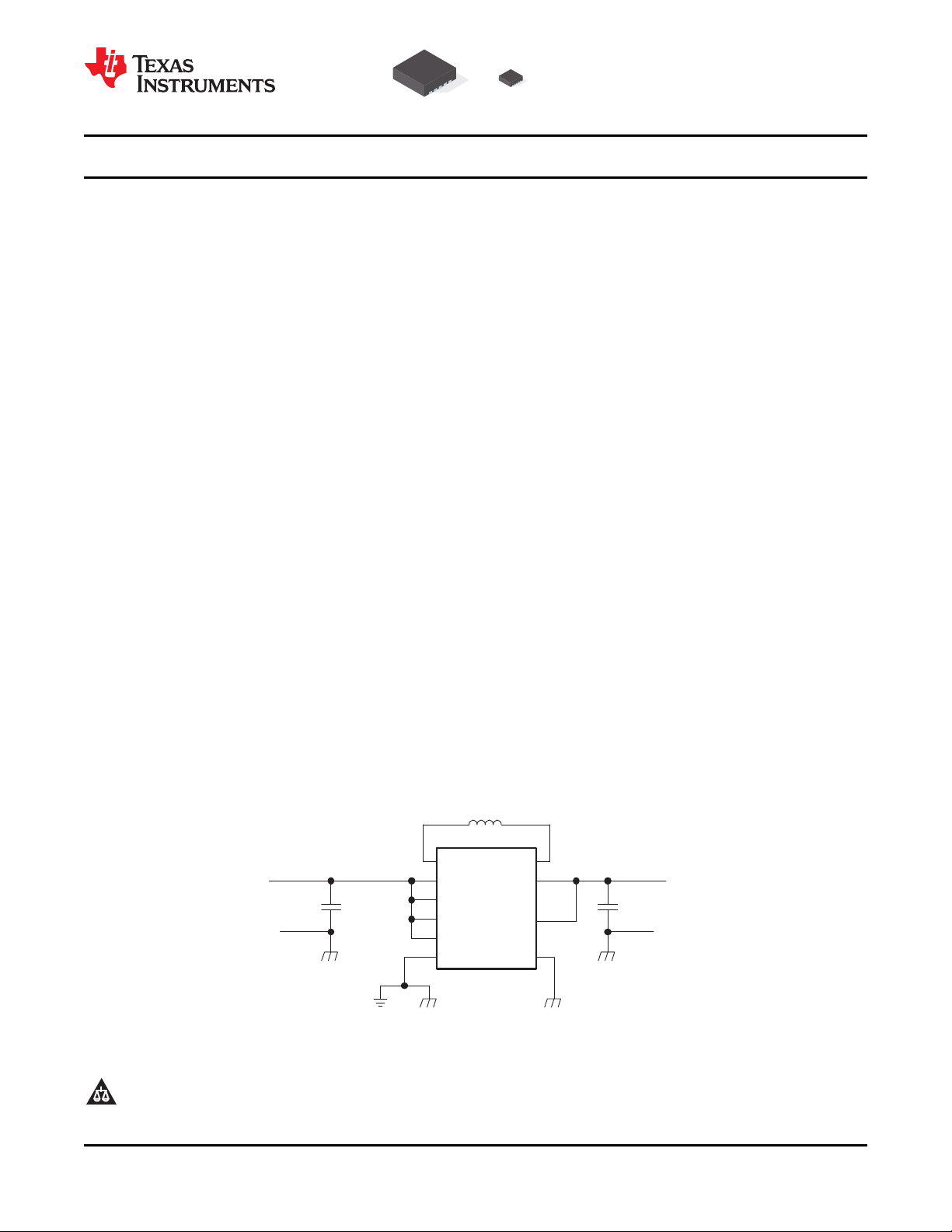
L1
VIN
VINA
EN
PS/SYNC
GND
L2
VOUT
FB
PGND
L1
2.2µH
C2
10µF
C1
10µF
V
IN
1.8Vto
5.5V
V
OUT
3.3Vupto
1200mA
TPS63001
www.ti.com
........................................................................................................................................................... SLVS520B – MARCH 2006 – REVISED JULY 2008
HIGH EFFICIENT SINGLE INDUCTOR BUCK-BOOST CONVERTER WITH 1.8-A SWITCHES
1
FEATURES APPLICATIONS
23
• Up to 96% Efficiency
• 1200-mA Output Current at 3.3V in Step Down
Mode (VIN = 3.6V to 5.5V)
• Up to 800-mA Output Current at 3.3V in Boost
Mode (VIN > 2.4V)
• Automatic Transition between Step Down and
Boost Mode
• Device Quiescent Current less than 50 µ A
• Input Voltage Range: 1.8V to 5.5V
• Fixed and Adjustable Output Voltage Options
from 1.2V to 5.5V
• Power Save Mode for Improved Efficiency at
Low Output Power
• Forced Fixed Frequency Operation and
Synchronization possible
• Load Disconnect During Shutdown
• Over-Temperature Protection
• Available in Small 3 mm × 3 mm, QFN-10
Package
• All Two-Cell and Three-Cell Alkaline, NiCd or
NiMH or Single-Cell Li Battery Powered
Products
• Portable Audio Players
• PDAs
• Cellular Phones
• Personal Medical Products
• White LEDs
DESCRIPTION
The TPS6300x devices provide a power supply
solution for products powered by either a two-cell or
three-cell alkaline, NiCd or NiMH battery, or a
one-cell Li-Ion or Li-polymer battery. Output currents
can go as high as 1200 mA while using a single-cell
Li-Ion or Li-Polymer Battery, and discharge it down to
2.5V or lower. The buck-boost converter is based on
a fixed frequency, pulse-width-modulation (PWM)
controller using synchronous rectification to obtain
maximum efficiency. At low load currents, the
converter enters Power Save mode to maintain high
efficiency over a wide load current range. The Power
Save mode can be disabled, forcing the converter to
operate at a fixed switching frequency. The maximum
average current in the switches is limited to a typical
value of 1800 mA. The output voltage is
programmable using an external resistor divider, or is
fixed internally on the chip. The converter can be
disabled to minimize battery drain. During shutdown,
the load is disconnected from the battery. The device
is packaged in a 10-pin QFN PowerPAD™ package
measuring 3 mm × 3 mm (DRC).
TPS63000
TPS63001
TPS63002
1
Please be aware that an important notice concerning availability, standard warranty, and use in critical applications of Texas Instruments semiconductor products and disclaimers thereto appears at the end of this data sheet.
2 PowerPAD is a trademark of Texas Instruments.
3 All other trademarks are the property of their respective owners.
PRODUCTION DATA information is current as of publication date.
Products conform to specifications per the terms of the Texas
Instruments standard warranty. Production processing does not
necessarily include testing of all parameters.
Copyright © 2006 – 2008, Texas Instruments Incorporated
Page 2
TPS63000
TPS63001
TPS63002
SLVS520B – MARCH 2006 – REVISED JULY 2008 ...........................................................................................................................................................
These devices have limited built-in ESD protection. The leads should be shorted together or the device placed in conductive foam
during storage or handling to prevent electrostatic damage to the MOS gates.
www.ti.com
AVAILABLE OUTPUT VOLTAGE OPTIONS
T
A
– 40 ° C to 85 ° C 3.3 V BPU 10-Pin QFN TPS63001DRC
(1) Contact the factory to check availability of other fixed output voltage versions.
(2) The DRC package is available taped and reeled. Add R suffix to device type (e.g., TPS63000DRCR) to order quantities of 3000 devices
per reel. Add T suffix to device type (e.g., TPS63000DRCT) to order quantities of 250 devices per reel.
OUTPUT VOLTAGE
DC/DC
Adjustable BPT TPS63000DRC
5.0 V BPV TPS63002DRC
PACKAGE MARKING PACKAGE PART NUMBER
(1)
ABSOLUTE MAXIMUM RATINGS
over operating free-air temperature range (unless otherwise noted)
Input voltage range on VIN, VINA, L1, L2, VOUT, PS/SYNC, EN, FB – 0.3 V to 7 V
Operating virtual junction temperature range, T
Storage temperature range T
(1) Stresses beyond those listed under absolute maximum ratings may cause permanent damage to the device. These are stress ratings
only, and functional operation of the device at these or any other conditions beyond those indicated under recommended operating
conditions is not implied. Exposure to absolute-maximum-rated conditions for extended periods my affect device reliability.
stg
J
(1)
TPS6300x
– 40 ° C to 150 ° C
– 65 ° C to 150 ° C
DISSIPATION RATINGS TABLE
PACKAGE
DRC 48.7 ° C/W 2054 mW 21 mW/ ° C
THERMAL RESISTANCE POWER RATING DERATING FACTOR ABOVE
Θ
JA
TA≤ 25 ° C TA= 25 ° C
(2)
RECOMMENDED OPERATING CONDITIONS
MIN NOM MAX UNIT
Supply voltage at VIN, VINA 1.8 5.5 V
Operating free air temperature range, T
Operating virtual junction temperature range, T
A
J
– 40 85 ° C
– 40 125 ° C
2 Submit Documentation Feedback Copyright © 2006 – 2008, Texas Instruments Incorporated
Product Folder Link(s): TPS63000 TPS63001 TPS63002
Page 3
www.ti.com
........................................................................................................................................................... SLVS520B – MARCH 2006 – REVISED JULY 2008
ELECTRICAL CHARACTERISTICS
over recommended free-air temperature range and over recommended input voltage range (typical at an ambient temperature
range of 25 ° C) (unless otherwise noted)
DC/DC STAGE
PARAMETER TEST CONDITIONS MIN TYP MAX UNIT
V
V
V
V
f Oscillator frequency 1250 1500 kHz
I
I
I
CONTROL STAGE
V
V
V
Input voltage range 1.8 5.5 V
I
Input voltage range for startup 1.9 5.5 V
I
TPS63000 output voltage range 1.2 5.5 V
O
TPS63000 feedback voltage 495 500 505 mV
FB
Frequency range for synchronization 1250 1800 kHz
Switch current limit VIN= V
SW
High side switch on resistance VIN= V
Low side switch on resistance VIN= V
= 3.6 V, TA= 25 ° C 1600 1800 2000 mA
INA
= 3.6 V 100 m Ω
INA
= 3.6 V 100 m Ω
INA
Line regulation 0.5%
Load regulation 0.5%
VIN 1 1.5 µ A
Quiescent IO= 0 mA, V
q
current V
VINA 40 50 µ A
VOUT (adjustable output voltage) 4 6 µ A
= 3.3 V
OUT
EN
= VIN= V
= 3.6 V,
INA
FB input impedance (fixed output voltage) 1 M Ω
Shutdown current V
S
Under voltage lockout threshold V
UVLO
EN, PS/SYNC input low voltage 0.4 V
IL
EN, PS/SYNC input high voltage 1.2 V
IH
= 0 V, VIN= V
EN
voltage decreasing 1.5 1.7 1.8 V
INA
= 3.6 V 0.1 1 µ A
INA
EN, PS/SYNC input current Clamped on GND or VINA 0.01 0.1 µ A
Overtemperature protection 140 ° C
Overtemperature hysteresis 20 ° C
TPS63000
TPS63001
TPS63002
Copyright © 2006 – 2008, Texas Instruments Incorporated Submit Documentation Feedback 3
Product Folder Link(s): TPS63000 TPS63001 TPS63002
Page 4
PGND
L1
VIN
EN
GND
L2
PS/SYNC
VINA
VOUT
FB
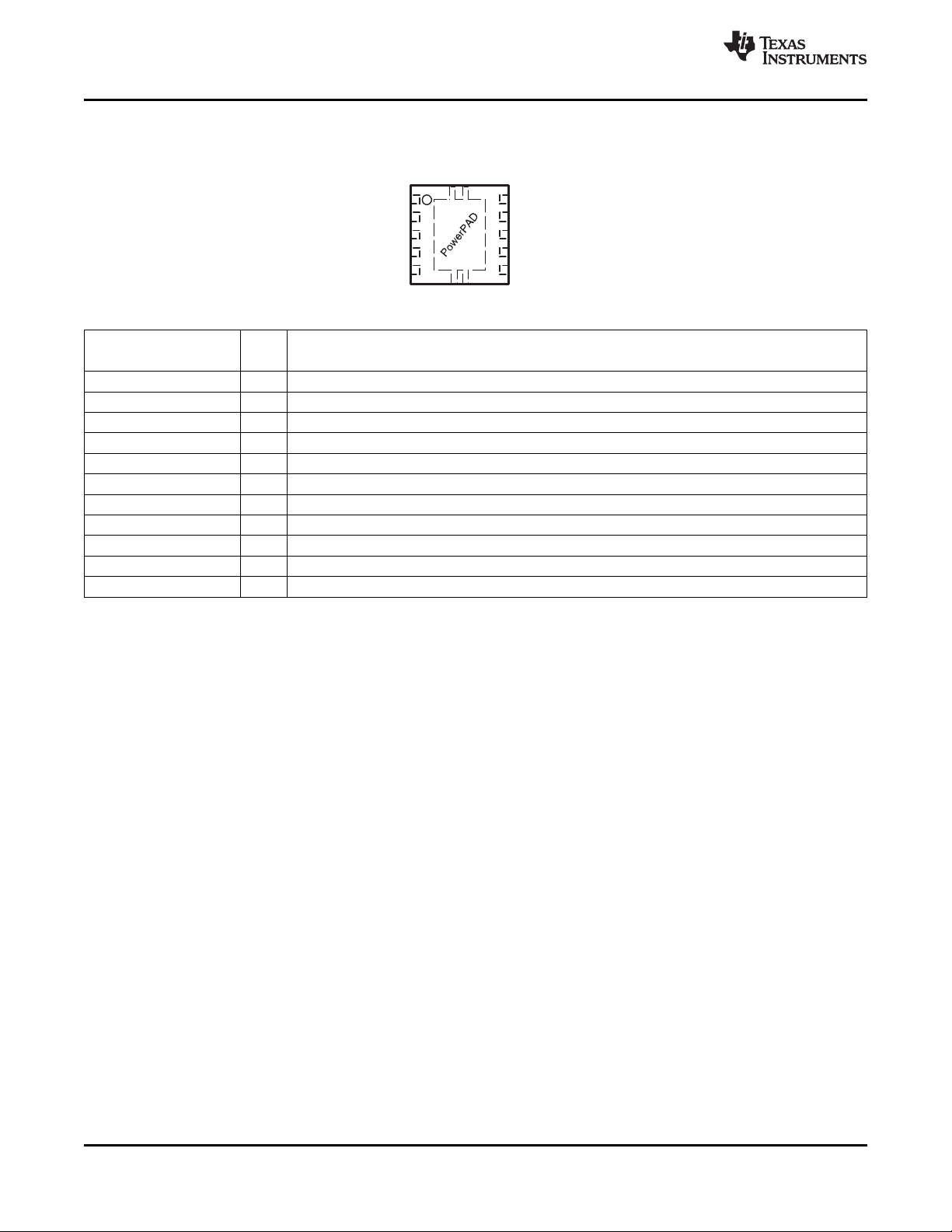
DRCPACKAGE
(TOP VIEW)
TPS63000
TPS63001
TPS63002
SLVS520B – MARCH 2006 – REVISED JULY 2008 ...........................................................................................................................................................
PIN ASSIGNMENTS
Terminal Functions
TERMINAL
NAME NO.
EN 6 I Enable input. (1 enabled, 0 disabled)
FB 10 I Voltage feedback of adjustable versions, must be connected to VOUT on fixed output voltage versions
GND 9 Control / logic ground
PS/SYNC 7 I Enable / disable power save mode (1 disabled, 0 enabled, clock signal for synchronization)
L1 4 I Connection for Inductor
L2 2 I Connection for Inductor
PGND 3 Power ground
VIN 5 I Supply voltage for power stage
VOUT 1 O Buck-boost converter output
VINA 8 I Supply voltage for control stage
PowerPAD™ Must be soldered to achieve appropriate power dissipation. Should be connected to PGND.
I/O DESCRIPTION
www.ti.com
4 Submit Documentation Feedback Copyright © 2006 – 2008, Texas Instruments Incorporated
Product Folder Link(s): TPS63000 TPS63001 TPS63002
Page 5
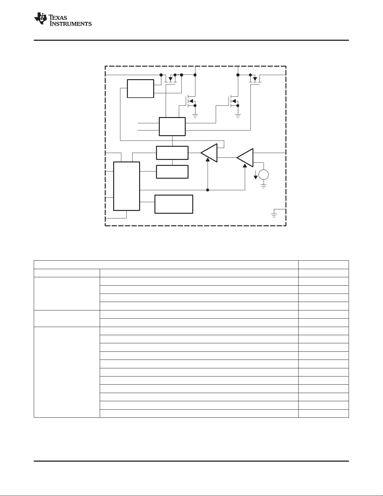
_
+
_
+
Current
Sensor
Gate
Control
PGND PGND
VBAT
VOUT
Modulator
+
-
Oscillator
Device
Control
Temperature
Control
VREF
PGND
PGND
FB
VOUT
L2L1
VIN
VINA
PS/SYNC
EN
GND
TPS63000
TPS63001
TPS63002
www.ti.com
........................................................................................................................................................... SLVS520B – MARCH 2006 – REVISED JULY 2008
FUNCTIONAL BLOCK DIAGRAM (TPS63000)
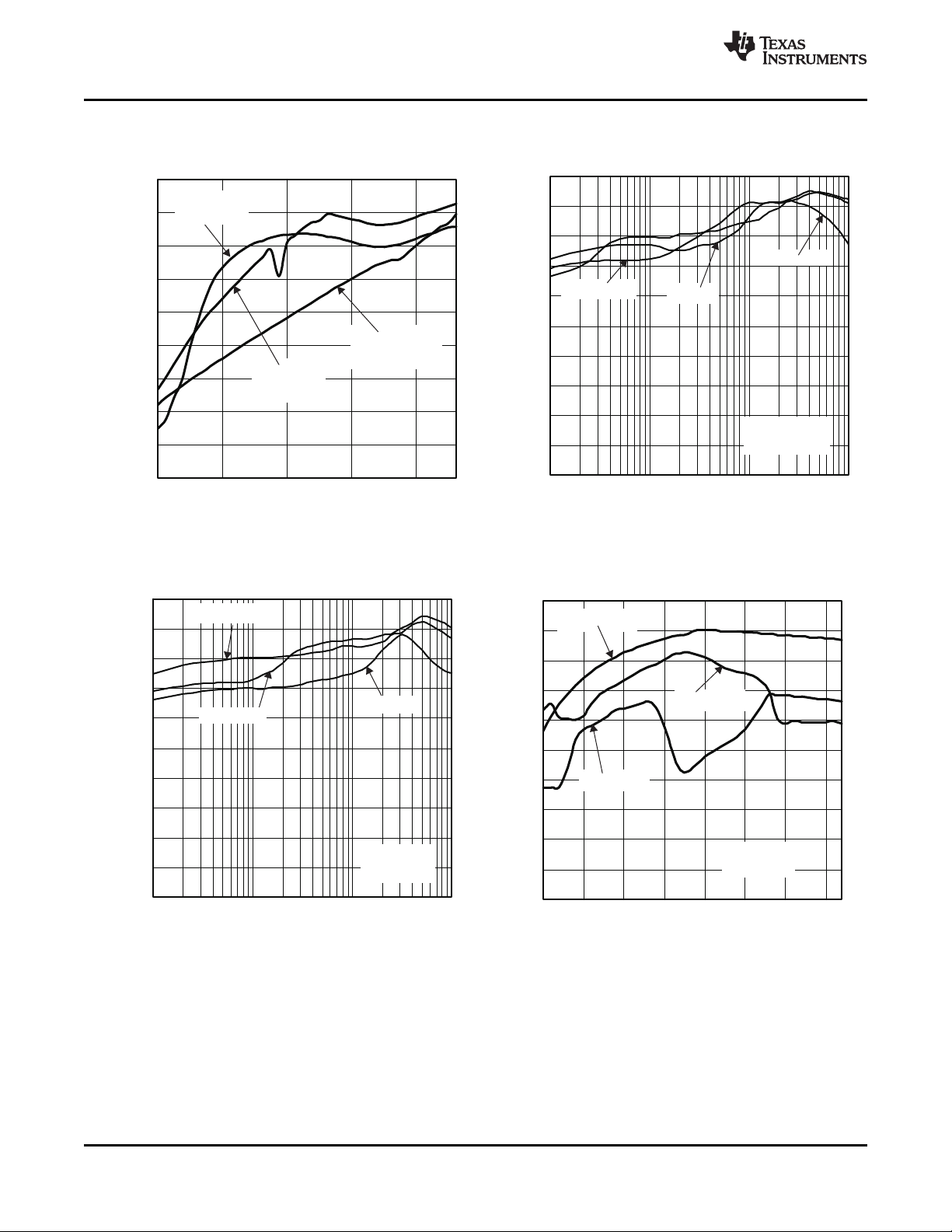
TYPICAL CHARACTERISTICS
TABLE OF GRAPHS
DESCRIPTION FIGURE
Maximum output current vs Input voltage 1
Efficiency vs Output current (TPS63001) 2
vs Output current (TPS63002) 3
vs Input voltage (TPS63001) 4
vs Input voltage (TPS63002) 5
Output voltage vs Output current (TPS63001) 6
vs Output current (TPS63002) 7
Waveforms Output voltage in continuous current mode (TPS63001, VIN > VOUT) 8
Output voltage in continuous current mode (TPS63001, VIN < VOUT) 9
Output voltage in continuous current mode (TPS63001, VIN = VOUT) 10
Copyright © 2006 – 2008, Texas Instruments Incorporated Submit Documentation Feedback 5
Output voltage in power save mode (TPS63001, VIN > VOUT) 11
Output voltage in power save mode (TPS63001, VIN < VOUT) 12
Load transient response (TPS63001, VIN > VOUT) 13
Load transient response (TPS63001, VIN < VOUT) 14
Line transient response (TPS63001, Iout = 300mA) 15
Line transient response (TPS63001, Iout = 600mA) 16
Startup after enable (TPS63000, VOUT = 2.5V) 17
Startup after enable (TPS63002) 18
Product Folder Link(s): TPS63000 TPS63001 TPS63002
Page 6
0
10
20
30
40
50
60
70
80
90
100
0.001 0.01
0.1 1
I - Ou tp ut Current- A
O
Efficiency-%
TPS63001
V =3.3V
O
V =4.2V
I
V =3.6V
I
V =2.4V
I
0
200
400
600
800
1000
1200
1400
1600
1800
1.8
2.6
3.4
4.2
5
V -InputVoltage-V
I
I -maximumoutputcurrent-mA
O
TPS63000,
V =1.8V
O
TPS63001,
V =3.3V
O
TPS63002,
V =5V
O
0
10
20
30
40
50
60
70
80
90
100
0.001
0.01
0.1
1
I -OutputCurrent- A
O
Efficiency-%
V =3.6V
I
V =4.2V
I
V =2.4V
I
TPS63002
V =5V
O
50
55
60
65
70
75
80
85
90
95
100
V -inputvoltage-V
I
Efficiency-%
1.8 2.82.3 3.3 3.8 4.3 5.34.8
TPS63001
V =3.3V
O
I =10mA
O
I =100mA
O
I =500mA
O
TPS63000
TPS63001
TPS63002
SLVS520B – MARCH 2006 – REVISED JULY 2008 ...........................................................................................................................................................
www.ti.com
MAXIMUM OUTPUT CURRENT EFFICIENCY
vs vs
INPUT VOLTAGE OUTPUT CURRENT (TPS63001)
Figure 1. Figure 2.
EFFICIENCY EFFICIENCY
vs vs
OUTPUT CURRENT (TPS63002) INPUT CURRENT (TPS63001)
6 Submit Documentation Feedback Copyright © 2006 – 2008, Texas Instruments Incorporated
Figure 3. Figure 4.
Product Folder Link(s): TPS63000 TPS63001 TPS63002
Page 7
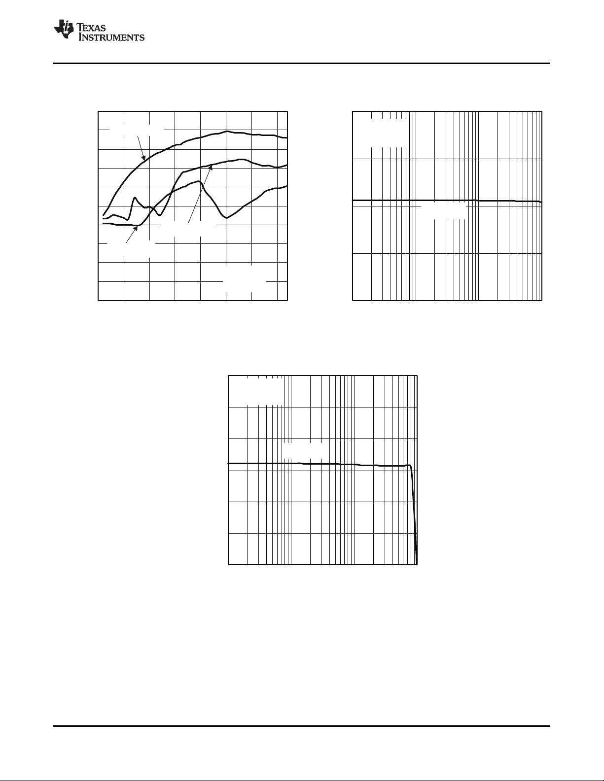
50
55
60
65
70
75
80
85
90
95
100
V -InputVoltage-V
I
Efficiency-%
TPS63002
V =5V
O
I =10mA
O
I =100mA
O
I =500mA
O
1.8 2.3 2.8 3.3 3.8 4.3 4.8 5.3
3.200
3.250
3.300
3.350
3.400
0.001 0.01
0.1
1
I -OutputCurrent- A
O
V -OutputVoltage-V
O
V =3.6V
I
TPS63001
V =3.3V
O
4.850
4.900
4.950
5
5.050
5.100
5.150
0.001 0.01 0.1 1
I -OutputCurrent- A
O
V -OutputVoltage-V
O
TPS63002
V =5V
O
V =3.6V
I
TPS63000
TPS63001
TPS63002
www.ti.com
........................................................................................................................................................... SLVS520B – MARCH 2006 – REVISED JULY 2008
EFFICIENCY OUTPUT VOLTAGE
vs vs
INPUT CURRENT (TPS63002) OUTPUT CURRENT (TPS63001)
Copyright © 2006 – 2008, Texas Instruments Incorporated Submit Documentation Feedback 7
Figure 5. Figure 6.
OUTPUT VOLTAGE
vs
OUTPUT CURRENT (TPS63002)
Figure 7.
Product Folder Link(s): TPS63000 TPS63001 TPS63002
Page 8
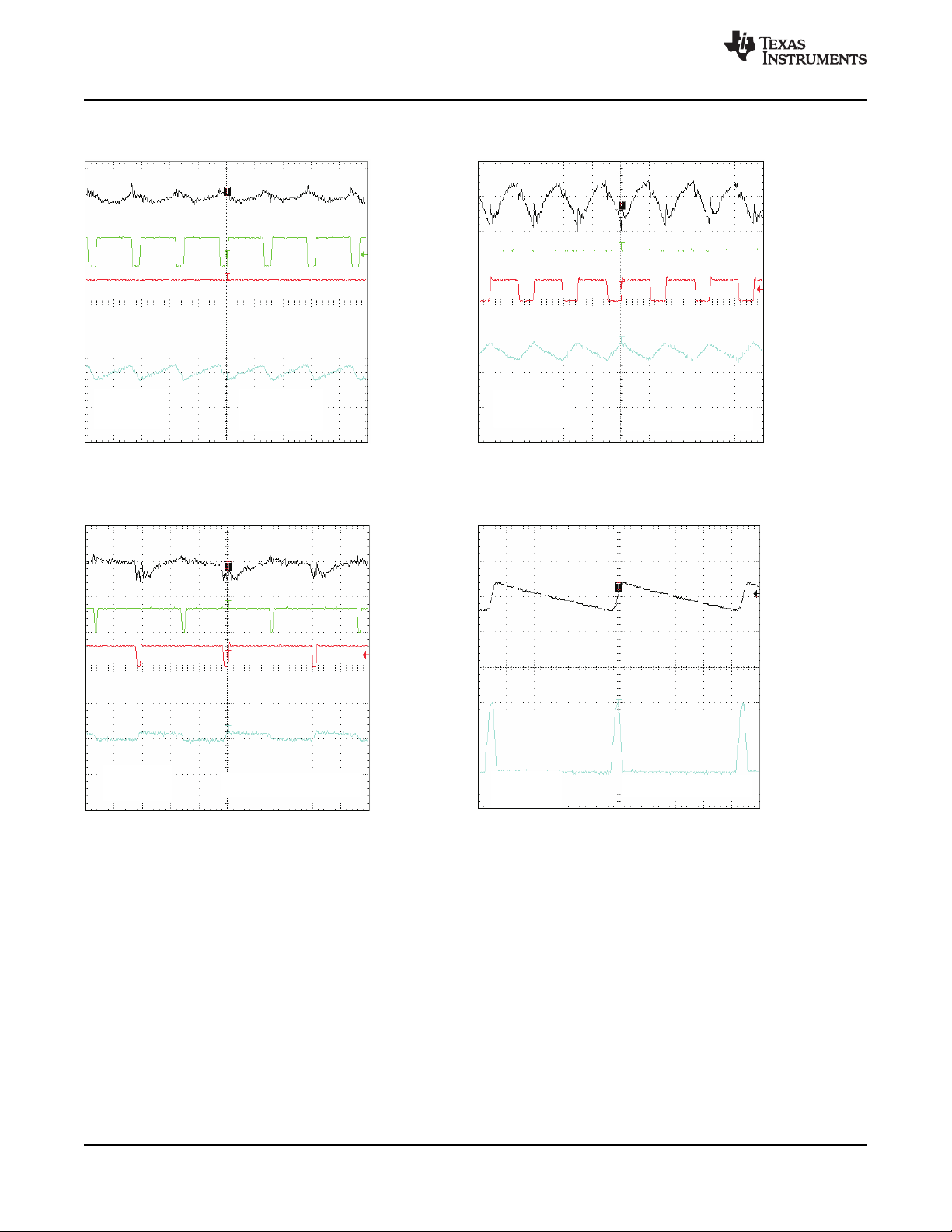
TPS63001
V =3.3V
O
V =4.2V,
I =500mA
I
O
InductorCurrent
500mA/div
L2Voltage
5V/div
L1Voltage
5V/div
OutputVoltage
10mV/div
Timebase500ns/div
V = 2.4V, I = 500 mA
I O
Timebase500ns/Div
TPS63001,
V =3.3V
O
OutputVoltage
10mV/div
L1Voltage
5V/div
L2Voltage
5V/div
InductorCurrent
500mA/div
InductorCurrent
500mA/div,dc
OutputVoltage
100mV/div
V =4.2V,I =50mA
I O
TPS63001,
V =3.3V
O
Timebase5 s/Divm
V =3.3V,I =500mA
I O
TPS63001,
V =3.3V
O
Timebase500ns/div
OutputVoltage
10mV/div
L1Voltage
5V/div
L2Voltage
5V/div
InductorCurrent
500mA/div
TPS63000
TPS63001
TPS63002
SLVS520B – MARCH 2006 – REVISED JULY 2008 ...........................................................................................................................................................
OUTPUT VOLTAGE IN CONTINUOUS OUTPUT VOLTAGE IN CONTINUOUS
CURRENT MODE (TPS63001, VIN > VOUT) CURRENT MODE (TPS63001, VIN > VOUT)
Figure 8. Figure 9.
www.ti.com
OUTPUT VOLTAGE IN CONTINUOUS OUTPUT VOLTAGE IN POWER
CURRENT MODE (TPS63001, VIN = VOUT) SAVE MODE (TPS63001, VIN > VOUT)
Figure 10. Figure 11.
8 Submit Documentation Feedback Copyright © 2006 – 2008, Texas Instruments Incorporated
Product Folder Link(s): TPS63000 TPS63001 TPS63002
Page 9

Timebase2ms/div
OutputVoltage
100mV/div,ac
OutputCurrent
200mA/div,dc
V =3.6V,
I =200mA to600mA
I
O
TPS63001,
V =3.3V
O
InductorCurrent
500mA/div,dc
OutputVoltage
100mV/div,ac
Ti me ba se 5 s/ divm
V =2.4V,I =50mA
I O
TPS63001,
V =3.3V
O
OutputVoltage
10mV/div,ac
InputVoltage
1V/div,dc
TPS63001,
V =3.3V
O
Timebase2ms/div
V =3Vto3.6V,
I =300mA
I
O
Timebase2ms/div
V =3V,
I =200mA to600mA
I
O
TPS63001,
V =3.3V
O
OutputVoltage
100mV/div,ac
OutputCurrent
200mA/div,dc
TPS63000
TPS63001
TPS63002
www.ti.com
........................................................................................................................................................... SLVS520B – MARCH 2006 – REVISED JULY 2008
OUTPUT VOLTAGE IN POWER LOAD TRANSIENT RESPONSE
SAVE MODE (TPS63001, VIN < VOUT) (TPS63001, VIN > VOUT)
Figure 12. Figure 13.
LOAD TRANSIENT RESPONSE LINE TRANSIENT RESPONSE
(TPS63001, VIN < VOUT) (TPS63001, Iout = 300mA)
Figure 14. Figure 15.
Copyright © 2006 – 2008, Texas Instruments Incorporated Submit Documentation Feedback 9
Product Folder Link(s): TPS63000 TPS63001 TPS63002
Page 10

V =3Vto3.6V,
I =600mA
I
O
TPS63001,
V =3.3V
O
Timebase2ms/div
OutputVoltage
20mV/div,ac
InputVoltage
1V/div,dc
OutputVoltage
1V/div,dc
Enable
2V/div,dc
InductorCurrent
200mA/div,dc
VoltageatL1
2V/div,dc
Timebase50 s/divm
V =3.3V,I =300mA
I O
TPS63000,
V =2.5V
O
VoltageatL2
2V/div,dc
TPS63002,
V =5V
O
InductorCurrent
500mA/div,dc
OutputVoltage
2V/div,dc
Timebase100 s/divm
Enable
2V/div,dc
V =2.4V,I =300mA
I O
TPS63000
TPS63001
TPS63002
SLVS520B – MARCH 2006 – REVISED JULY 2008 ...........................................................................................................................................................
LINE TRANSIENT RESPONSE STARTUP AFTER ENABLE
(TPS63001, Iout = 600mA) (TPS63000, VOUT = 2.5V)
www.ti.com
Figure 16. Figure 17.
STARTUP AFTER ENABLE
(TPS63002)
Figure 18.
10 Submit Documentation Feedback Copyright © 2006 – 2008, Texas Instruments Incorporated
Product Folder Link(s): TPS63000 TPS63001 TPS63002
Page 11

L1
VIN
VINA
EN
PS/SYNC
GND
L2
VOUT
FB
PGND
L1
R1
R2
C2
R3
C3
C1
V
IN
V
OUT
TPS6300X
www.ti.com
........................................................................................................................................................... SLVS520B – MARCH 2006 – REVISED JULY 2008
PARAMETER MEASUREMENT INFORMATION
List of Components
REFERENCE DESCRIPTION MANUFACTURER
TPS6300 0 / 1 / 2 Texas Instruments
L1 VLF4012-2R2 TDK
C1 10 µ F 6.3V, 0603, X7R ceramic
C2 2 × 10 µ F 6.3V, 0603, X7R ceramic
C3 0.1 µ F, X7R ceramic
R3 100 Ω
R1, R2 Depending on the output voltage at TPS63000, not used at TPS6300 1 / 2
TPS63000
TPS63001
TPS63002
Copyright © 2006 – 2008, Texas Instruments Incorporated Submit Documentation Feedback 11
Product Folder Link(s): TPS63000 TPS63001 TPS63002
Page 12

TPS63000
TPS63001
TPS63002
SLVS520B – MARCH 2006 – REVISED JULY 2008 ...........................................................................................................................................................
DETAILED DESCRIPTION
CONTROLLER CIRCUIT
The controlling circuit of the device is based on an average current mode topology. The average inductor current
is regulated by a fast current regulator loop which is controlled by a voltage control loop. The controller also uses
input and output voltage feedforward. Changes of input and output voltage are monitored and immediately can
change the duty cycle in the modulator to achieve a fast response to those errors. The voltage error amplifier
gets its feedback input from the FB pin. At adjustable output voltages a resistive voltage divider must be
connected to that pin. At fixed output voltages FB must be connected to the output voltage to directly sense the
voltage. Fixed output voltage versions use a trimmed internal resistive divider. The feedback voltage will be
compared with the internal reference voltage to generate a stable and accurate output voltage.
The controller circuit also senses the average input current as well as the peak input current. With this, maximum
input power can be controlled as well as the maximum peak current to achieve a safe and stable operation under
all possible conditions. To finally protect the device from overheating, an internal temperature sensor is
implemented.
Synchronous Operation
The device uses 4 internal N-channel MOSFETs to maintain synchronous power conversion at all possible
operating conditions. This enables the device to keep high efficency over a wide input voltage and output power
range.
To avoid ground shift problems due to the high currents in the switches, two separate ground pins GND and
PGND are used. The reference for all control functions is the GND pin. The power switches are connected to
PGND. Both grounds must be connected on the PCB at only one point ideally close to the GND pin. Due to the
4-switch topology, the load is always disconnected from the input during shutdown of the converter.
www.ti.com
Buck-Boost Operation
To be able to regulate the output voltage properly at all possible input voltage conditions, the device
automatically switches from step down operation to boost operation and back as required by the configuration. It
always uses one active switch, one rectifying switch, one switch permanently on, and one switch permanently off.
Therefore, it operates as a step down converter (buck) when the input voltage is higher than the output voltage,
and as a boost converter when the input voltage is lower than the output voltage. There is no mode of operation
in which all 4 switches are permanently switching. Controlling the switches this way allows the converter to
maintain high efficiency at the most important point of operation; when input voltage is close to the output
voltage. The RMS current through the switches and the inductor is kept at a minimum, to minimize switching and
conduction losses. Switching losses are also kept low by using only one active and one passive switch.
Regarding the remaining 2 switches, one is kept permanently on and the other is kept permanently off, thus
causing no switching losses.
Power Save Mode and Synchronization
The PS/SYNC pin can be used to select different operation modes. To enable power save, PS/SYNC must be
set low. Power save mode is used to improve efficiency at light load. If power save mode is enabled, the
converter stops operating if the average inductor current gets lower than about 300 mA and the output voltage is
at or above its nominal value. If the output voltage decreases below its nominal value, the device ramps up the
output voltage again by starting operation using a programmed average inductor current higher than required by
the current load condition. Operation can last for one or several pulses. The converter again stops operating
once the conditions for stopping operation are met again.
The power save mode can be disabled by programming high at the PS/SYNC. Connecting a clock signal at
PS/SYNC forces the device to synchronize to the connected clock frequency. Synchronization is done by a PLL,
so synchronizing to lower and higher frequencies compared to the internal clock works without any issues. The
PLL can also tolerate missing clock pulses without the converter malfunctioning. The PS/SYNC input supports
standard logic thresholds.
12 Submit Documentation Feedback Copyright © 2006 – 2008, Texas Instruments Incorporated
Product Folder Link(s): TPS63000 TPS63001 TPS63002
Page 13

TPS63000
TPS63001
TPS63002
www.ti.com
Device Enable
The device is put into operation when EN is set high. It is put into a shutdown mode when EN is set to GND. In
shutdown mode, the regulator stops switching, all internal control circuitry is switched off, and the load is
disconnected from the input. This also means that the output voltage can drop below the input voltage during
shutdown. During start-up of the converter, the duty cycle and the peak current are limited in order to avoid high
peak currents flowing from the input.
Softstart and Short Circuit Protection
After being enabled, the device starts operating. The average current limit ramps up from an initial 400mA
following the output voltage increasing. At an output voltage of about 1.2 V, the current limit is at its nominal
value. If the output voltage does not increase, the current limit will not increase. There is no timer implemented.
Thus the output voltage overshoot at startup, as well as the inrush current, is kept at a minimum. The device
ramps up the output voltage in a controlled manner even if a very large capacitor is connected at the output.
When the output voltage does not increase above 1.2 V, the device assumes a short circuit at the output and
keeps the current limit low to protect itself and the application. At a short at the output during operation the
current limit also will be decreased accordingly. At 0 V at the output, for example, the output current will not
exceed about 400 mA.
Undervoltage Lockout
An undervoltage lockout function prevents device start-up if the supply voltage on VINA is lower than
approximately its threshold (see electrical characteristics table). When in operation, the device automatically
enters the shutdown mode if the voltage on VINA drops below the undervoltage lockout threshold. The device
automatically restarts if the input voltage recovers to the minimum operating input voltage.
........................................................................................................................................................... SLVS520B – MARCH 2006 – REVISED JULY 2008
Overtemperature Protection
The device has a built-in temperature sensor which monitors the internal IC temperature. If the temperature
exceeds the programmed threshold (see electrical characteristics table) the device stops operating. As soon as
the IC temperature has decreased below the programmed threshold, it starts operating again. There is a built-in
hysteresis to avoid unstable operation at IC temperatures at the overtemperature threshold.
Copyright © 2006 – 2008, Texas Instruments Incorporated Submit Documentation Feedback 13
Product Folder Link(s): TPS63000 TPS63001 TPS63002
Page 14

R1+ R
2
ǒ
V
OUT
V
FB
* 1
Ǔ
C
ff
+
2.2 ms
R
1
L1
VIN
VINA
EN
PS/SYNC
GND
L2
VOUT
FB
PGND
L1
R1
R2
C2
R3
C3
C1
V
IN
V
OUT
TPS6300X
TPS63000
TPS63001
TPS63002
SLVS520B – MARCH 2006 – REVISED JULY 2008 ...........................................................................................................................................................
APPLICATION INFORMATION
DESIGN PROCEDURE
The TPS6300x dc/dc converters are intended for systems powered by one-cell Li-Ion or Li-Polymer battery with a
typical voltage between 2.3 V and 4.5 V. They can also be used in systems powered by a double or triple cell
Alkaline, NiCd, or NiMH battery with a typical terminal voltage between 1.8 V and 5.5 V . Additionally, any other
voltage source with a typical output voltage between 1.8 V and 5.5 V can power systems where the TPS6300x is
used.
PROGRAMMING THE OUTPUT VOLTAGE
Within the TPS6300X family there are fixed and adjustable output voltage versions available. To properly
configure the fixed output voltage devices, the FB pin is used to sense the output voltage. This means that it
must be connected directly to VOUT. At the adjustable output voltage versions, an external resistor divider is
used to adjust the output voltage. The resistor divider must be connected between VOUT, FB and GND. When
the output voltage is regulated properly, the typical value of the voltage at the FB pin is 500mV. The maximum
recommended value for the output voltage is 5.5V. The current through the resistive divider should be about 100
times greater than the current into the FB pin. The typical current into the FB pin is 0.01 µ A, and the voltage
across the resistor between FB and GND, R2, is typically 500 mV. Based on those two values, the recommended
value for R
to keep the value for this resistor in the range of 200k Ω . From that, the value of the resistor connected between
VOUT and FB, R1, depending on the needed output voltage (V
should be lower than 500k Ω , in order to set the divider current at 1 µ A or higher. It is recommended
2
), can be calculated using Equation 1 :
OUT
www.ti.com
If as an example, an output voltage of 3.3 V is needed, a 1.0 M Ω resistor should be chosen for R1. To improve
control performance using a feedforward capacitor in parallel to R
is recommended. The value for the
1
feedforward capacitor can be calculated using Equation 2 .
Figure 19. Typical Application Circuit for Adjustable Output Voltage Option
INDUCTOR SELECTION
To properly configure the TPS6300X devices, an inductor must be connected between pin L1 and pin L2. To
estimate the inductance value Equation 3 and Equation 4 can be used.
(1)
(2)
14 Submit Documentation Feedback Copyright © 2006 – 2008, Texas Instruments Incorporated
Product Folder Link(s): TPS63000 TPS63001 TPS63002
Page 15

L
1
+
V
OUT
ǒ
V
IN1
* V
OUT
Ǔ
V
IN1
f 0.3 A
L
2
+
V
in2
ǒ
V
OUT
* V
IN2
Ǔ
V
OUT
f 0.3 A
I
1
+
I
OUT
0.8
)
V
OUT
ǒ
V
IN1
* V
OUT
Ǔ
2 V
IN1
f L
I
2
+
V
OUT
I
OUT
0.8 V
IN2
)
V
IN2
ǒ
V
OUT
* V
IN2
Ǔ
2 V
OUT
f L
TPS63000
TPS63001
TPS63002
www.ti.com
In both equations f is the minimum switching frequency. In Equation 3 the minimum inductance value, L1for step
down mode operation is calculated. V
L2, for boost mode operation is calculated. V
inductor value is either L1or L2whichever is higher. As an example, a suitable inductor for generating 3.3V from
a Li-Ion battery with a battery voltage range from 2.5V up to 4.2V is 2.2 µ H. The recommended inductor value
range is between 1.5 µ H and 4.7 µ H. In general, this means that at high voltage conversion rates, higher inductor
values offer better performance.
With the chosen inductance value, the peak current for the inductor in steady state operation can be calculated.
Equation 5 shows how to calculate the peak current I1in step down mode operation and Equation 6 shows how
to calculate the peak current I2in boost mode operation.
........................................................................................................................................................... SLVS520B – MARCH 2006 – REVISED JULY 2008
is the maximum input voltage. In Equation 4 the minimum inductance,
IN1
is the minimum input voltage. The recommended minimum
IN2
(3)
(4)
(5)
The critical current value for selecting the right inductor is the higher value of I1and I2. It also needs to be taken
into account that load transients and error conditions may cause higher inductor currents. This also needs to be
taken into account when selecting an appropriate inductor. The following inductor series from different suppliers
have been used with TPS6300x converters:
Table 1. List of Inductors
VENDOR INDUCTOR SERIES
Coilcraft
Murata LQH3NP
Tajo Yuden NR3015
TDK
LPS3015
LPS4012
VLF3215
VLF4012
CAPACITOR SELECTION
Input Capacitor
At least a 4.7 µ F input capacitor is recommended to improve transient behavior of the regulator and EMI
behavior of the total power supply circuit. A ceramic capacitor placed as close as possible to the VIN and PGND
pins of the IC is recommended.
Output Capacitor
For the output capacitor, it is recommended to use small ceramic capacitors placed as close as possible to the
VOUT and PGND pins of the IC. If, for any reason, the application requires the use of large capacitors which can
not be placed close to the IC, using a smaller ceramic capacitor in parallel to the large one is recommended.
This small capacitor should be placed as close as possible to the VOUT and PGND pins of the IC.
To get an estimate of the recommended minimum output capacitance, Equation 7 can be used.
(6)
Copyright © 2006 – 2008, Texas Instruments Incorporated Submit Documentation Feedback 15
Product Folder Link(s): TPS63000 TPS63001 TPS63002
Page 16

C
OUT
+ 5 L
mF
mH
P
D(MAX)
+
T
J(MAX)
* T
A
R
qJA
+
125°C * 85°C
48.7 °CńW
+ 820 mW
TPS63000
TPS63001
TPS63002
SLVS520B – MARCH 2006 – REVISED JULY 2008 ...........................................................................................................................................................
A capacitor with a value in the range of the calculated minimum should be used. This is required to maintain
control loop stability. There are no additional requirements regarding minimum ESR. There is also no upper limit
for the output capacitance value. Larger capacitors will cause lower output voltage ripple as well as lower output
voltage drop during load transients.
LAYOUT CONSIDERATIONS
As for all switching power supplies, the layout is an important step in the design, especially at high peak currents
and high switching frequencies. If the layout is not carefully done, the regulator could show stability problems as
well as EMI problems. Therefore, use wide and short traces for the main current path and for the power ground
tracks. The input capacitor, output capacitor, and the inductor should be placed as close as possible to the IC.
Use a common ground node for power ground and a different one for control ground to minimize the effects of
ground noise. Connect these ground nodes at any place close to one of the ground pins of the IC.
The feedback divider should be placed as close as possible to the control ground pin of the IC. To lay out the
control ground, it is recommended to use short traces as well, separated from the power ground traces. This
avoids ground shift problems, which can occur due to superimposition of power ground current and control
ground current.
www.ti.com
(7)
THERMAL INFORMATION
Implementation of integrated circuits in low-profile and fine-pitch surface-mount packages typically requires
special attention to power dissipation. Many system-dependent issues such as thermal coupling, airflow, added
heat sinks and convection surfaces, and the presence of other heat-generating components affect the
power-dissipation limits of a given component.
Three basic approaches for enhancing thermal performance are listed below.
• Improving the power dissipation capability of the PCB design
• Improving the thermal coupling of the component to the PCB by soldering the PowerPAD
• Introducing airflow in the system
The maximum recommended junction temperature (T
resistance of the 10-pin QFN 3 × 3 package (DRC) is R
regulator operation is assured to a maximum ambient temperature T
dissipation is about 820mW, as calculated in Equation 8 . More power can be dissipated if the maximum ambient
temperature of the application is lower.
) of the TPS6300x devices is 125 ° C. The thermal
J
= 48.7 ° C/W, if the PowerPAD is soldered. Specified
θ JA
of 85 ° C. Therefore, the maximum power
A
(8)
16 Submit Documentation Feedback Copyright © 2006 – 2008, Texas Instruments Incorporated
Product Folder Link(s): TPS63000 TPS63001 TPS63002
Page 17

PACKAGE OPTION ADDENDUM
www.ti.com
29-Jul-2008
PACKAGING INFORMATION
Orderable Device Status
(1)
Package
Type
Package
Drawing
Pins Package
Qty
Eco Plan
TPS63000DRCR ACTIVE SON DRC 10 3000 Green (RoHS &
no Sb/Br)
TPS63000DRCRG4 ACTIVE SON DRC 10 3000 Green (RoHS &
no Sb/Br)
TPS63000DRCT ACTIVE SON DRC 10 250 Green (RoHS &
no Sb/Br)
TPS63000DRCTG4 ACTIVE SON DRC 10 250 Green (RoHS &
no Sb/Br)
TPS63001DRCR ACTIVE SON DRC 10 3000 Green (RoHS &
no Sb/Br)
TPS63001DRCRG4 ACTIVE SON DRC 10 3000 Green (RoHS &
no Sb/Br)
TPS63001DRCT ACTIVE SON DRC 10 250 Green (RoHS &
no Sb/Br)
TPS63001DRCTG4 ACTIVE SON DRC 10 250 Green (RoHS &
no Sb/Br)
TPS63002DRCR ACTIVE SON DRC 10 3000 Green (RoHS &
no Sb/Br)
TPS63002DRCRG4 ACTIVE SON DRC 10 3000 Green (RoHS &
no Sb/Br)
TPS63002DRCT ACTIVE SON DRC 10 250 Green (RoHS &
no Sb/Br)
TPS63002DRCTG4 ACTIVE SON DRC 10 250 Green (RoHS &
no Sb/Br)
(1)
The marketing status values are defined as follows:
ACTIVE: Product device recommended for new designs.
LIFEBUY: TI has announced that the device will be discontinued, and a lifetime-buy period is in effect.
NRND: Not recommended for new designs. Device is in production to support existing customers, but TI does not recommend using this part in
a new design.
PREVIEW: Device has been announced but is not in production. Samples may or may not be available.
OBSOLETE: TI has discontinued the production of the device.
(2)
Lead/Ball Finish MSL Peak Temp
CU NIPDAU Level-2-260C-1YEAR
CU NIPDAU Level-2-260C-1YEAR
CU NIPDAU Level-2-260C-1YEAR
CU NIPDAU Level-2-260C-1YEAR
CU NIPDAU Level-2-260C-1YEAR
CU NIPDAU Level-2-260C-1YEAR
CU NIPDAU Level-2-260C-1YEAR
CU NIPDAU Level-2-260C-1YEAR
CU NIPDAU Level-2-260C-1YEAR
CU NIPDAU Level-2-260C-1YEAR
CU NIPDAU Level-2-260C-1YEAR
CU NIPDAU Level-2-260C-1YEAR
(3)
(2)
Eco Plan - The planned eco-friendly classification: Pb-Free (RoHS), Pb-Free (RoHS Exempt), or Green (RoHS & no Sb/Br) - please check
http://www.ti.com/productcontent for the latest availability information and additional product content details.
TBD: The Pb-Free/Green conversion plan has not been defined.
Pb-Free (RoHS): TI's terms "Lead-Free" or "Pb-Free" mean semiconductor products that are compatible with the current RoHS requirements
for all 6 substances, including the requirement that lead not exceed 0.1% by weight in homogeneous materials. Where designed to be soldered
at high temperatures, TI Pb-Free products are suitable for use in specified lead-free processes.
Pb-Free (RoHS Exempt): This component has a RoHS exemption for either 1) lead-based flip-chip solder bumps used between the die and
package, or 2) lead-based die adhesive used between the die and leadframe. The component is otherwise considered Pb-Free (RoHS
compatible) as defined above.
Green (RoHS & no Sb/Br): TI defines "Green" to mean Pb-Free (RoHS compatible), and free of Bromine (Br) and Antimony (Sb) based flame
retardants (Br or Sb do not exceed 0.1% by weight in homogeneous material)
(3)
MSL, Peak Temp. -- The Moisture Sensitivity Level rating according to the JEDEC industry standard classifications, and peak solder
temperature.
Important Information and Disclaimer:The information provided on this page represents TI's knowledge and belief as of the date that it is
provided. TI bases its knowledge and belief on information provided by third parties, and makes no representation or warranty as to the
accuracy of such information. Efforts are underway to better integrate information from third parties. TI has taken and continues to take
reasonable steps to provide representative and accurate information but may not have conducted destructive testing or chemical analysis on
incoming materials and chemicals. TI and TI suppliers consider certain information to be proprietary, and thus CAS numbers and other limited
information may not be available for release.
Addendum-Page 1
Page 18

PACKAGE OPTION ADDENDUM
www.ti.com
In no event shall TI's liability arising out of such information exceed the total purchase price of the TI part(s) at issue in this document sold by TI
to Customer on an annual basis.
29-Jul-2008
Addendum-Page 2
Page 19

PACKAGE MATERIALS INFORMATION
www.ti.com
TAPE AND REEL INFORMATION
30-Jul-2008
*All dimensions are nominal
Device Package
Type
TPS63000DRCR SON DRC 10 3000 330.0 12.4 3.3 3.3 1.1 8.0 12.0 Q2
TPS63000DRCT SON DRC 10 250 180.0 12.4 3.3 3.3 1.1 8.0 12.0 Q2
TPS63001DRCR SON DRC 10 3000 330.0 12.4 3.3 3.3 1.1 8.0 12.0 Q2
TPS63001DRCT SON DRC 10 250 180.0 12.4 3.3 3.3 1.1 8.0 12.0 Q2
TPS63002DRCR SON DRC 10 3000 330.0 12.4 3.3 3.3 1.1 8.0 12.0 Q2
TPS63002DRCT SON DRC 10 250 180.0 12.4 3.3 3.3 1.1 8.0 12.0 Q2
Package
Drawing
Pins SPQ Reel
Diameter
(mm)
Reel
Width
W1 (mm)
A0 (mm) B0 (mm) K0 (mm) P1
(mm)W(mm)
Pin1
Quadrant
Pack Materials-Page 1
Page 20

PACKAGE MATERIALS INFORMATION
www.ti.com
30-Jul-2008
*All dimensions are nominal
Device Package Type Package Drawing Pins SPQ Length (mm) Width (mm) Height (mm)
TPS63000DRCR SON DRC 10 3000 346.0 346.0 29.0
TPS63000DRCT SON DRC 10 250 190.5 212.7 31.8
TPS63001DRCR SON DRC 10 3000 346.0 346.0 29.0
TPS63001DRCT SON DRC 10 250 190.5 212.7 31.8
TPS63002DRCR SON DRC 10 3000 346.0 346.0 29.0
TPS63002DRCT SON DRC 10 250 190.5 212.7 31.8
Pack Materials-Page 2
Page 21

Page 22

Page 23
Page 24

IMPORTANT NOTICE
Texas Instruments Incorporated and its subsidiaries (TI) reserve the right to make corrections, modifications, enhancements, improvements,
and other changes to its products and services at any time and to discontinue any product or service without notice. Customers should
obtain the latest relevant information before placing orders and should verify that such information is current and complete. All products are
sold subject to TI’s terms and conditions of sale supplied at the time of order acknowledgment.
TI warrants performance of its hardware products to the specifications applicable at the time of sale in accordance with TI’s standard
warranty. Testing and other quality control techniques are used to the extent TI deems necessary to support this warranty. Except where
mandated by government requirements, testing of all parameters of each product is not necessarily performed.
TI assumes no liability for applications assistance or customer product design. Customers are responsible for their products and
applications using TI components. To minimize the risks associated with customer products and applications, customers should provide
adequate design and operating safeguards.
TI does not warrant or represent that any license, either express or implied, is granted under any TI patent right, copyright, mask work right,
or other TI intellectual property right relating to any combination, machine, or process in which TI products or services are used. Information
published by TI regarding third-party products or services does not constitute a license from TI to use such products or services or a
warranty or endorsement thereof. Use of such information may require a license from a third party under the patents or other intellectual
property of the third party, or a license from TI under the patents or other intellectual property of TI.
Reproduction of TI information in TI data books or data sheets is permissible only if reproduction is without alteration and is accompanied
by all associated warranties, conditions, limitations, and notices. Reproduction of this information with alteration is an unfair and deceptive
business practice. TI is not responsible or liable for such altered documentation. Information of third parties may be subject to additional
restrictions.
Resale of TI products or services with statements different from or beyond the parameters stated by TI for that product or service voids all
express and any implied warranties for the associated TI product or service and is an unfair and deceptive business practice. TI is not
responsible or liable for any such statements.
TI products are not authorized for use in safety-critical applications (such as life support) where a failure of the TI product would reasonably
be expected to cause severe personal injury or death, unless officers of the parties have executed an agreement specifically governing
such use. Buyers represent that they have all necessary expertise in the safety and regulatory ramifications of their applications, and
acknowledge and agree that they are solely responsible for all legal, regulatory and safety-related requirements concerning their products
and any use of TI products in such safety-critical applications, notwithstanding any applications-related information or support that may be
provided by TI. Further, Buyers must fully indemnify TI and its representatives against any damages arising out of the use of TI products in
such safety-critical applications.
TI products are neither designed nor intended for use in military/aerospace applications or environments unless the TI products are
specifically designated by TI as military-grade or "enhanced plastic." Only products designated by TI as military-grade meet military
specifications. Buyers acknowledge and agree that any such use of TI products which TI has not designated as military-grade is solely at
the Buyer's risk, and that they are solely responsible for compliance with all legal and regulatory requirements in connection with such use.
TI products are neither designed nor intended for use in automotive applications or environments unless the specific TI products are
designated by TI as compliant with ISO/TS 16949 requirements. Buyers acknowledge and agree that, if they use any non-designated
products in automotive applications, TI will not be responsible for any failure to meet such requirements.
Following are URLs where you can obtain information on other Texas Instruments products and application solutions:
Products Applications
Amplifiers amplifier.ti.com Audio www.ti.com/audio
Data Converters dataconverter.ti.com Automotive www.ti.com/automotive
DSP dsp.ti.com Broadband www.ti.com/broadband
Clocks and Timers www.ti.com/clocks Digital Control www.ti.com/digitalcontrol
Interface interface.ti.com Medical www.ti.com/medical
Logic logic.ti.com Military www.ti.com/military
Power Mgmt power.ti.com Optical Networking www.ti.com/opticalnetwork
Microcontrollers microcontroller.ti.com Security www.ti.com/security
RFID www.ti-rfid.com Telephony www.ti.com/telephony
RF/IF and ZigBee® Solutions www.ti.com/lprf Video & Imaging www.ti.com/video
Mailing Address: Texas Instruments, Post Office Box 655303, Dallas, Texas 75265
Copyright © 2008, Texas Instruments Incorporated
Wireless www.ti.com/wireless
 Loading...