

Page 1

C1
38V MAX
VIN SW
FB
GND
CTRL
COMP
C2
20 mA
TPS61161A
ON/OFF
DIMMING
CONTROL
V 3 V to 18 V
I
L1
22 Hm
1 Fm
C3
220 nF
R
10
set
W
1 Fm
L1: TDK VLCF5020T-220MR75-1
C1: Murata GRM188R61E105K
C2: Murata GRM21BR71H105K
D1: ONsemi MBR0540T1
D1
Product
Folder
Sample &
Buy
Technical
Documents
Tools &
Software
Support &
Community
SLVS937B –MARCH 2009–REVISED NOVEMBER2014
TPS6116xA White LED Driver with PWM Brightness Control in
2-mm x 2-mm WSON Package
1 Features 3 Description
1
• Input Voltage Range: 2.7 V to 18 V
• 26-V Open LED Protection for TPS61160A
38-V Open LED Protection for TPS61161A
• 200mV Reference Voltage With ±2% Accuracy
• PWM Interface for Brightness Control
• Built-in Soft Start
• Up to 90% Efficiency
• 2-mm × 2-mm × 0.8-mm 6-Pin WSON Package
With Thermal Pad
2 Applications
• Cellular Phones
• Portable Media Players
• Ultra Mobile Devices
• GPS Receivers
• White LED Backlighting for Media Form Factor
Display
With a 40-V rated integrated switch FET, the
TPS61160A/61A is a boost converter that drives
LEDs in series. The boost converter runs at 600-kHz
fixed switching frequency to reduce output ripple,
improve conversion efficiency, and allows for the use
of small external components.
The default white LED current is set with the external
sensor resistor Rset, and the feedback voltage is
regulated to 200 mV, as shown in the typical
application. During the operation, the LED current can
be controlled by a pulse width modulation (PWM)
signal applied to the CTRL pin through which the duty
cycle determines the feedback reference voltage. In
PWM dimming mode, the TPS61160A/61A does not
burst the LED current; therefore, it does not generate
audible noises on the output capacitor. For maximum
protection, the device features integrated open LED
protection that disables the TPS61160A/61A to
prevent the output from exceeding the absolute
maximum ratings during open LED conditions.
The TPS61160A/61A is available in a space-saving,
2-mm × 2-mm WSON package with thermal pad.
TPS61160A,TPS61161A
1
An IMPORTANT NOTICE at the end of this data sheet addresses availability, warranty, changes, use in safety-critical applications,
intellectual property matters and other important disclaimers. PRODUCTION DATA.
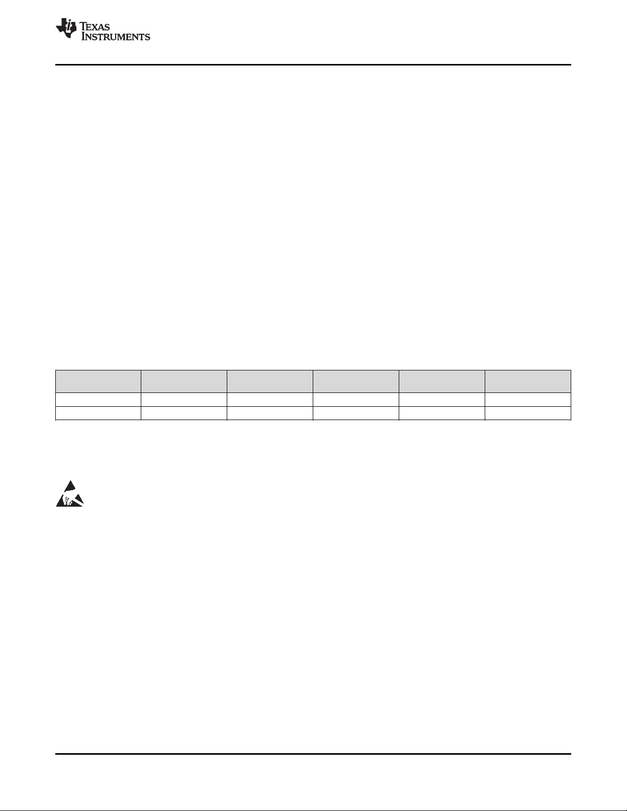
Device Information
PART NUMBER PACKAGE OPEN LED PROTECTION
TPS61160A TPS61160A use 26 V (typical)
TPS61161A TPS61161A use 38 V (typical)
(1) For all available packages, see the orderable addendum at
the end of the datasheet.
WSON (6)
(1)
Typical Application of TPS61161A
Page 2

TPS61160A,TPS61161A
SLVS937B –MARCH 2009–REVISED NOVEMBER 2014
www.ti.com
Table of Contents
1 Features.................................................................. 1
2 Applications ........................................................... 1
3 Description ............................................................. 1
4 Revision History..................................................... 2
5 Pin Configuration and Functions......................... 3
6 Specifications......................................................... 3
6.1 Absolute Maximum Ratings ...................................... 3
6.2 Handling Ratings....................................................... 4
6.3 Recommended Operating Conditions....................... 4
6.4 Thermal Information.................................................. 4
6.5 Dissipation Ratings ................................................... 4
6.6 Electrical Characteristics........................................... 5
6.7 Typical Characteristics.............................................. 6
7 Detailed Description .............................................. 8
7.1 Overview ................................................................... 8
7.2 Functional Block Diagram......................................... 8
7.3 Feature Description................................................... 8
7.4 Device Functional Modes........................................ 10
8 Application and Implementation ........................ 11
8.1 Application Information............................................ 11
8.2 Typical Applications ................................................ 11
9 Power Supply Recommendations...................... 19
10 Layout................................................................... 20
10.1 Layout Guidelines ................................................. 20
10.2 Layout Example .................................................... 20
10.3 Thermal Considerations........................................ 20
11 Device and Documentation Support................. 21
11.1 Device Support...................................................... 21
11.2 Documentation Support ........................................ 21
11.3 Related Links ........................................................ 21
11.4 Trademarks........................................................... 21
11.5 Electrostatic Discharge Caution............................ 21
11.6 Glossary................................................................ 21
12 Mechanical, Packaging, and Orderable
Information........................................................... 21
4 Revision History
NOTE: Page numbers for previous revisions may differ from page numbers in the current version.
Changes from Revision A (July 2011) to Revision B Page
• Added Device Information and Handling Rating tables, Feature Description, Device Functional Modes, Application
and Implementation, Power Supply Recommendations, Layout, Device and Documentation Support, and
Mechanical, Packaging, and Orderable Information sections; moved some curves to Application Curves section;
change "QFN" to "SON" ......................................................................................................................................................... 1
• Changed (reversed) the Vi=5V and Vi=3.6V characteristic labels in Figure 3....................................................................... 6
Changes from Original (March 2009) to Revision A Page
• Deleted "6 LEDs" and "10 LEDs" from the second feature bullet for TPS61160A and TPS61161A Open-LED
Protection, respectively........................................................................................................................................................... 1
• Deleted "for up to 10 LEDs in Series" from title ..................................................................................................................... 1
• Added "38V Max" to Typical Application of TPS61161A, top of LED string........................................................................... 1
• Changed from "...for driving up to 10 white LED" to "...for driving white LED" in first sentence of OPERATION section. .... 8
• Changed text of last sentence in "OPEN LED PROTECTION" section to clarify circuit description...................................... 9
• Changed Figure 11 to show separate terminals for COMP and FB..................................................................................... 10
• Changed Li-Ion Driver for 6 White LEDs With External PWM Dimming Network to clarify schematic................................ 14
2 Submit Documentation Feedback Copyright © 2009–2014, Texas Instruments Incorporated
Product Folder Links: TPS61160A TPS61161A
Page 3
www.ti.com
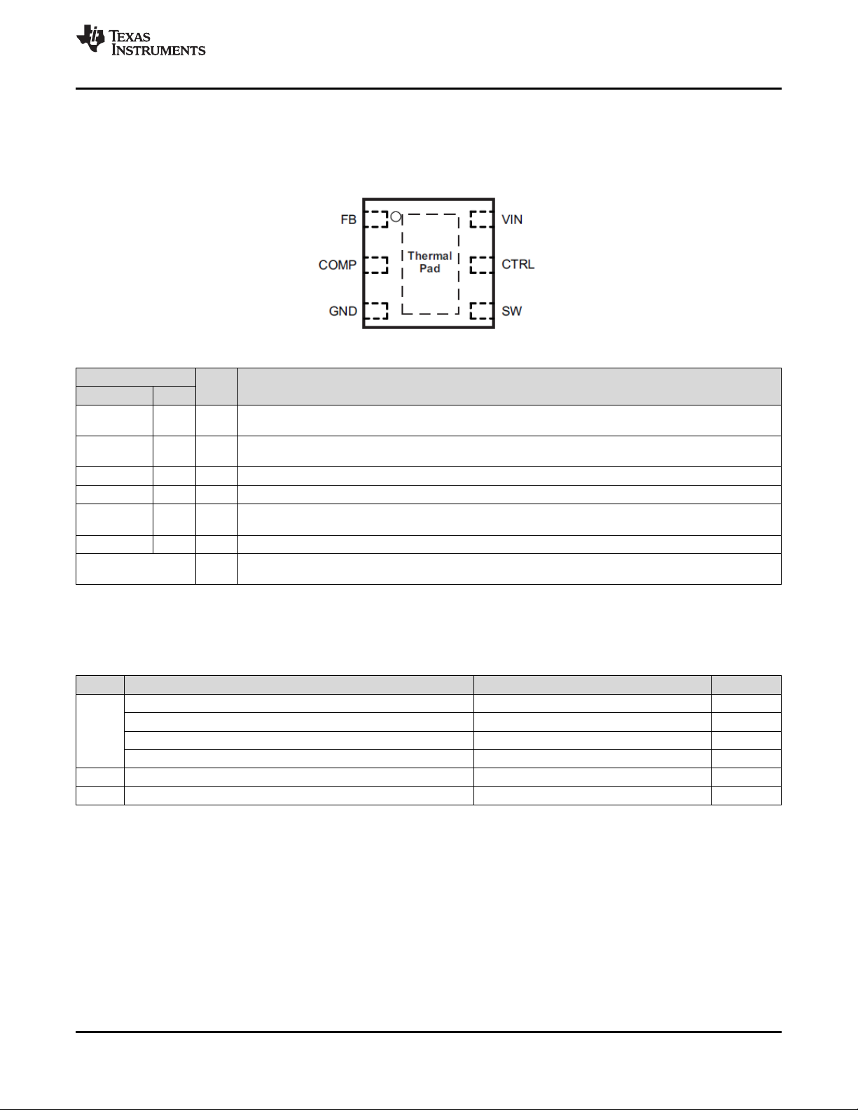
5 Pin Configuration and Functions
TPS61160A,TPS61161A
SLVS937B –MARCH 2009–REVISED NOVEMBER 2014
WSON (DRV) Package
6 Pins
Top View
Pin Functions
PIN
NAME NO.
COMP 2 O
CTRL 5 I
FB 1 I Feedback pin for current. Connect the sense resistor from FB to GND.
GND 3 O Ground
SW 4 I
VIN 6 I The input supply pin for the IC. Connect VIN to a supply voltage between 2.7 V and 18 V.
Thermal Pad
I/O DESCRIPTION
Output of the transconductance error amplifier. Connect an external capacitor to this pin to compensate the
regulator.
Control pin of the boost regulator. Enable and disable IC. PWM signal can be applied to the pin for LED
brightness dimming as well.
This is the switching node of the IC. Connect the inductor between the VIN and SW pin. This pin is also
used to sense the output voltage for open LED protection
The thermal pad should be soldered to the analog ground plane. If possible, use thermal via to connect to
ground plane for ideal power dissipation.
6 Specifications
6.1 Absolute Maximum Ratings
over operating free-air temperature range (unless otherwise noted)
Supply voltages on VIN
V
Voltages on CTRL
I
Voltage on FB and COMP
Voltage on SW
P
T
Continuous power dissipation See Dissipation Ratings
D
Operating junction temperature –40 150 °C
J
(1) Stresses beyond those listed under Absolute Maximum Ratings may cause permanent damage to the device. These are stress ratings
only, and functional operation of the device at these or any other conditions beyond those indicated under Recommended Operating
Conditions is not implied. Exposure to absolute-maximum-rated conditions for extended periods may affect device reliability.
(2) All voltage values are with respect to network ground terminal.
(2)
(2)
(2)
(2)
(1)
MIN MAX UNIT
–0.3 20 V
–0.3 20 V
–0.3 3 V
–0.3 40 V
Copyright © 2009–2014, Texas Instruments Incorporated Submit Documentation Feedback 3
Product Folder Links: TPS61160A TPS61161A
Page 4
TPS61160A,TPS61161A
SLVS937B –MARCH 2009–REVISED NOVEMBER 2014
www.ti.com
6.2 Handling Ratings
MIN MAX UNIT
T
V
Storage temperature range –65 150 °C
stg
Human body model (HBM), per ANSI/ESDA/JEDEC JS-001, all 4000
(1)
Electrostatic discharge V
(ESD)
pins
Charged device model (CDM), per JEDEC specification 1000
JESD22-C101, all pins
(2)
(1) JEDEC document JEP155 states that 500-V HBM allows safe manufacturing with a standard ESD control process.
(2) JEDEC document JEP157 states that 250-V CDM allows safe manufacturing with a standard ESD control process.
6.3 Recommended Operating Conditions
MIN MAX UNIT
V
I
V
O
L Inductor
f
dim
Duty
C
IN
C
O
T
A
T
J
(1) These values are recommended values that have been successfully tested in several applications. Other values may be acceptable in
(2) The device can support the frequency range from 1 kHz to 5 kHz, based on the specification, t
Input voltage, V
IN
Output voltage V
(1)
PWM dimming frequency
(2)
2.7 18 V
IN
10 22 μH
5 100 kHz
PWM duty cycle resolution 10 kHz 0.5%
30 kHz 1.5%
Input capacitor 1 μF
Output capacitor
(1)
0.47 10 μF
Operating ambient temperature –40 85 °C
Operating junction temperature –40 125 °C
other applications but should be fully tested by the user.
. The output ripple needs to be
considered in the range of 1 kHz to 5 kHz.
off
38 V
6.4 Thermal Information
TPS61160A,
THERMAL METRIC
(1)
TPS61161A
DRV
UNIT
6 PINS
R
θJA
R
θJC(top)
Junction-to-ambient thermal resistance 140
Junction-to-case (top) thermal resistance 20
°C/W
(1) For more information about traditional and new thermal metrics, see the IC Package Thermal Metrics application report, SPRA953.
6.5 Dissipation Ratings
BOARD PACKAGE R
(1)
Low-K
High-K
DRV 20°C/W 140°C/W 7.1 mW/°C 715 mW 395 mW 285 mW
(2)
DRV 20°C/W 65°C/W 15.4 mW/°C 1540 mW 845 mW 615 mW
θJC
R
θJA
(1) The JEDEC low-K (1s) board used to derive this data was a 3 in × 3 in, two-layer board with 2-ounce copper traces on top of the board.
(2) The JEDEC high-K (2s2p) board used to derive this data was a 3 in × 3 in, multilayer board with 1-ounce internal power and ground
planes and 2-ounce copper traces on top and bottom of the board.
DERATING FACTOR
ABOVE TA= 25°C
TA< 25°C TA= 70°C TA= 85°C
4 Submit Documentation Feedback Copyright © 2009–2014, Texas Instruments Incorporated
Product Folder Links: TPS61160A TPS61161A
Page 5
TPS61160A,TPS61161A
www.ti.com
SLVS937B –MARCH 2009–REVISED NOVEMBER 2014
6.6 Electrical Characteristics
VIN= 3.6 V, CTRL = VIN; for Min/Max values TA= –40°C to 85°C, typical values are at TA= 25°C (unless otherwise noted)
PARAMETER TEST CONDITIONS MIN TYP MAX UNIT
SUPPLY CURRENT
V
I
I
Q
I
SD
UVLO Undervoltage lockout threshold VIN falling 2.2 2.5 V
V
hys
ENABLE AND REFERENCE CONTROL
V
(CTRLh)
V
(CTRLl)
R
(CTRL)
t
off
VOLTAGE AND CURRENT CONTROL
V
REF
V
(REF_PWM)
I
FB
f
S
D
max
t
min_on
I
sink
I
source
G
ea
R
ea
f
ea
POWER SWITCH
R
DS(on)
I
LN_NFET
OC and OLP
I
LIM
I
LIM_Start
t
Half_LIM
V
ovp
V
(FB_OVP)
t
REF
t
step
THERMAL SHUTDOWN
T
shutdown
T
hysteresis
Input voltage range, V
IN
Operating quiescent current into V
Device PWM switching no load 1.8 mA
IN
2.7 18 V
Shutdown current CRTL = GND, VIN= 4.2 V 1 μA
Undervoltage lockout hysteresis 70 mV
CTRL logic high voltage VIN= 2.7 V to 18 V 1.2 V
CTRL logic low voltage VIN= 2.7 V to 18 V 0.4 V
CTRL pull down resistor 400 800 1600 kΩ
CTRL pulse width to shutdown CTRL high to low 2.5 ms
Voltage feedback regulation voltage 196 200 204 mV
Voltage feedback regulation voltage VFB= 50 mV 47 50 53 mV
under brightness control
VFB= 20 mV 17 20 23
Voltage feedback input bias current VFB= 200 mV 2 μA
Oscillator frequency 500 600 700 kHz
Maximum duty cycle VFB= 100 mV 90% 93%
Minimum on pulse width 40 ns
Comp pin sink current 100 μA
Comp pin source current 100 μA
Error amplifier transconductance 240 320 400 μmho
Error amplifier output resistance 6 MΩ
Error amplifier crossover frequency 5 pF connected to COMP 500 kHz
N-channel MOSFET on-resistance VIN= 3.6 V 0.3 0.6
VIN= 3 V 0.7
N-channel leakage current VSW= 35 V, TA= 25°C 1 μA
N-Channel MOSFET current limit D = D
Start up current limit D = D
max
max
0.56 0.7 0.84 A
0.4 A
Time step for half current limit 5 ms
Open LED protection threshold Measured on the SW pin, 25 26 27 V
TPS61160A 37 38 39
TPS61161A
Open LED protection threshold on FB Measured on the FB pin, percentage
of Vref, 50%
Vref = 200 mV and 20 mV
V
filter time constant 180 μs
REF
V
ramp up time 213 μs
REF
Thermal shutdown threshold 160 °C
Thermal shutdown threshold hysteresis 15 °C
Ω
Copyright © 2009–2014, Texas Instruments Incorporated Submit Documentation Feedback 5
Product Folder Links: TPS61160A TPS61161A
Page 6
40
50
60
70
80
90
100
0 10 20 30 40 50
10 LEDs - TPS61161A
V = 12 V
I
Output Current - mA
Efficiency - %
V = 5 V
I
V = 3.6 V
I
300
400
500
600
700
800
900
1000
20 30 40 50 60 70 80 90
DutyCycle-%
SwitchCurrentLimit-mA
40
50
60
70
80
90
100
0 10 20 30 40 50
OutputCurrent-mA
4(12.8V),6(19.2V)LEDs
8(25.6V),10(32V)LEDs
6LEDs
V =3.6V
I
4LEDs
8LEDs
10LEDs
Efficiency-%
40
50
60
70
80
90
100
0 10 20 30 40 50
6LEDs- TPS61160A
V =3.6V
I
V =3V
I
V =4.2V
I
OutputCurrent-mA
Efficiency-%
TPS61160A,TPS61161A
SLVS937B –MARCH 2009–REVISED NOVEMBER 2014
6.7 Typical Characteristics
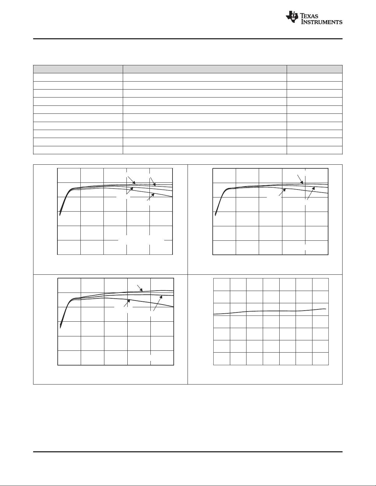
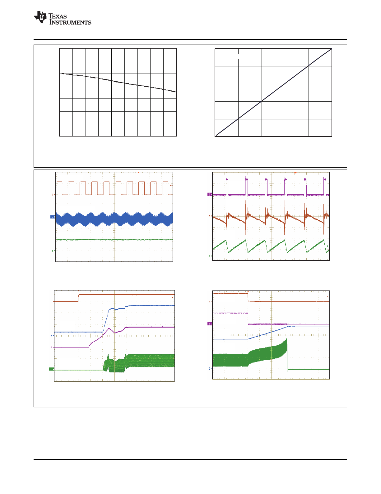
Table 1. Table of Graphs
FIGURE
Efficiency TPS61160A/61A VIN= 3.6 V; 4, 6, 8, 10 LEDs; L = 22 μH Figure 1
Efficiency TPS61160A Figure 2
Efficiency TPS61161A Figure 3
Current limit TA= 25°C Figure 4
Current limit Figure 5
PWM dimming linearity VIN= 3.6 V; PWM Freq = 10 kHz and 40 kHz Figure 6
Output ripple at PWM dimming 8 LEDs; VIN= 3.6 V; I
Switching waveform 8 LEDs; VIN= 3.6 V; I
Start-up 8 LEDs; VIN= 3.6 V; I
Open LED protection 8 LEDs; VIN= 3.6 V; I
= 20 mA; PWM Freq = 10 kHz Figure 7
LOAD
= 20 mA; L = 22 μH Figure 8
LOAD
= 20 mA; L =22 μH Figure 9
LOAD
= 20 mA; L = 22 μH Figure 10
LOAD
www.ti.com
Figure 1. Efficiency vs Output Current
Figure 3. Efficiency vs Output Current Figure 4. Switch Current Limit vs Duty Cycle
6 Submit Documentation Feedback Copyright © 2009–2014, Texas Instruments Incorporated
Figure 2. Efficiency vs Output Current
Product Folder Links: TPS61160A TPS61161A
Page 7
t-2ms/div
CTRL
5V/div
VOUT
10V/div
COMP
500mV/div
I
200mA/div
L
t-100 s/divm
OPENLED
5V/div
FB
200mV/div
VOUT
10V/div
I
200mA/div
L
t-100 s/divm
PWM2V/div
VOUT 20mV/div AC
I 10mA/div
LED
t-1 s/divm
SW
20V/div
VOUT
20mV/div
AC
I
200mA/div
L
0
40
80
120
160
200
0 20 40 60 80 100
PWMDutyCycle-%
10kHz,40kHz
FBVoltage-mV
300
400
500
600
700
800
900
1000
-40 -20 0 20 40 60 80 100 120 140
Temperature- C°
SwitchCurrentLimit-mA
www.ti.com
TPS61160A,TPS61161A
SLVS937B –MARCH 2009–REVISED NOVEMBER 2014
Figure 5. Switch Current Limit vs Temperature
Figure 7. Output Ripple at PWM Dimming
Figure 6. FB Voltage vs PWM Duty Cycle
Figure 8. Switching Waveform
Copyright © 2009–2014, Texas Instruments Incorporated Submit Documentation Feedback 7
Figure 9. Start-Up
Figure 10. Open LED Protection
Product Folder Links: TPS61160A TPS61161A
Page 8
SW
Ramp
Generator
Oscillator
Current
Sensor
OLP
CTRL
GND
C3
L1
+
FB
Reference
Control
D1
Error
Amplifer
2
1
Rset
C2
Vin
C1
PWM Control
4
6
Soft
Start-up
5
3
COMP
TPS61160A,TPS61161A
SLVS937B –MARCH 2009–REVISED NOVEMBER 2014
www.ti.com
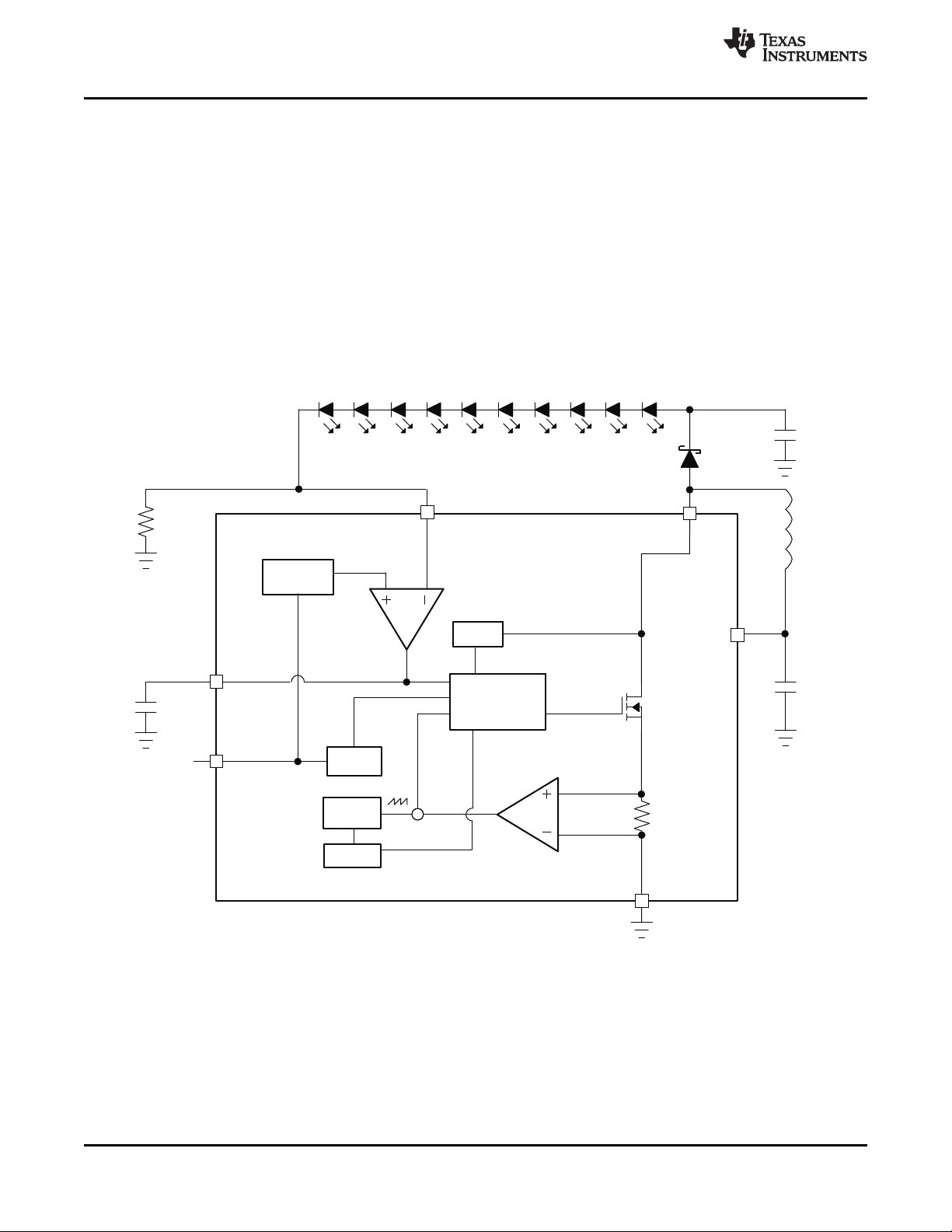
7 Detailed Description
7.1 Overview
The TPS61160A/61A is a high-efficiency, high output voltage boost converter in small package size that is ideal
for driving white LED in series. The serial LED connection provides even illumination by sourcing the same
output current through all LEDs, eliminating the need for expensive factory calibration. The device integrates 40V/0.7-A switch FET and operates in pulse width modulation (PWM) with 600-kHz fixed switching frequency. For
operation see the block diagram. The duty cycle of the converter is set by the error amplifier output and the
current signal applied to the PWM control comparator. The control architecture is based on traditional currentmode control; therefore, a slope compensation is added to the current signal to allow stable operation for duty
cycles larger than 50%. The feedback loop regulates the FB pin to a low reference voltage (200 mV typical),
reducing the power dissipation in the current sense resistor.
7.2 Functional Block Diagram
7.3 Feature Description
7.3.1 Soft Start-Up
Soft-start circuitry is integrated into the IC to avoid a high inrush current during start-up. After the device is
enabled, the voltage at FB pin ramps up to the reference voltage in 32 steps, each step takes 213 μs. This
ensures that the output voltage rises slowly to reduce the input current. Additionally, for the first 5 msec after the
COMP voltage ramps, the current limit of the switch is set to half of the normal current limit spec. During this
period, the input current is kept below 400 mA (typical). See the start-up waveform of a typical example,
Figure 9.
8 Submit Documentation Feedback Copyright © 2009–2014, Texas Instruments Incorporated
Product Folder Links: TPS61160A TPS61161A
Page 9

V Duty 200 mV
u
FB
LED
SET
V
R
TPS61160A,TPS61161A
www.ti.com
SLVS937B –MARCH 2009–REVISED NOVEMBER 2014
Feature Description (continued)
7.3.2 Open LED Protection
Open LED protection circuitry prevents IC damage as the result of white LED disconnection. The
TPS61160A/61A monitors the voltage at the SW pin and FB pin during each switching cycle. The circuitry turns
off the switch FET and shuts down the IC when both of the following conditions persist for 8 switching clock
cycles: (1) the SW voltage exceeds the V
voltage. As a result, the output voltage falls to the level of the input supply. The device remains in shutdown
mode until it is enabled by toggling the CTRL pin logic. To allow the use of inexpensive low-voltage output
capacitor, the TPS61160A/61A has different open lamp protection thresholds. The threshold is set at 26 V for the
TPS61160A and 38 V for the TPS61161A. Select the appropriate device so that the product of the number of
external LEDs and each LED's maximum forward voltage plus the 200 mV reference voltage does not exceed
the minimum OVP threshold or (n
LEDS
X V
7.3.3 Shutdown
The TPS61160A/61A enters shutdown mode when the CTRL voltage is logic low for more than 2.5 ms. During
shutdown, the input supply current for the device is less than 1 μA (max). Although the internal FET does not
switch in shutdown, there is still a DC current path between the input and the LEDs through the inductor and
Schottky diode. The minimum forward voltage of the LED array must exceed the maximum input voltage to
ensure that the LEDs remain off in shutdown; however, in the typical application with two or more LEDs, the
forward voltage is large enough to reverse bias the Schottky and keep leakage current low.
7.3.4 Current Program
The FB voltage is regulated by a low 0.2-V reference voltage. The LED current is programmed externally using a
current-sense resistor in series with the LED string. The value of the RSET is calculated using Equation 1:
threshold and (2) the FB voltage is less than half of regulation
OVP
LED(MAX)
) + 200 mV ≤ V
OVP(MIN).
where
• I
• VFB= regulated voltage of FB
• R
= output current of LEDs
LED
= current sense resistor (1)
SET
The output current tolerance depends on the FB accuracy and the current sensor resistor accuracy.
7.3.5 PWM Brightness Dimming
When the CTRL pin is constantly high, the FB voltage is regulated to 200 mV typically. However, the CTRL pin
allows a PWM signal to reduce this regulation voltage; therefore, it achieves LED brightness dimming. The
relationship between the duty cycle and FB voltage is given by Equation 2.
where
• Duty = duty cycle of the PWM signal
• 200 mV = internal reference voltage (2)
As shown in Figure 11, the IC chops up the internal 200-mV reference voltage at the duty cycle of the PWM
signal. The pulse signal is then filtered by an internal low pass filter. The output of the filter is connected to the
error amplifier as the reference voltage for the FB pin regulation. Therefore, although a PWM signal is used for
brightness dimming, only the WLED DC current is modulated, which is often referred as analog dimming. This
eliminates the audible noise which often occurs when the LED current is pulsed in replica of the frequency and
duty cycle of PWM control. Unlike other scheme which filters the PWM signal for analog dimming,
TPS61160A/61A regulation voltage is independent of the PWM logic voltage level which often has large
variations.
For optimum performance, use the PWM dimming frequency in the range of 5 kHz to 100 kHz. The requirement
of minimum dimming frequency comes from the output ripple. Low frequency causes high output ripple. Since the
CTRL pin is logic only pin, applying an external RC filter to the pin does not work.
Copyright © 2009–2014, Texas Instruments Incorporated Submit Documentation Feedback 9
Product Folder Links: TPS61160A TPS61161A
Page 10

VBG
200 mV
Error
Amplifier
FB
CTRL
COMP
TPS61160A,TPS61161A
SLVS937B –MARCH 2009–REVISED NOVEMBER 2014
www.ti.com
Feature Description (continued)
Figure 11. Block Diagram of Programmable FB Voltage Using PWM Signal
To use lower PWM dimming, add an external RC network connected to the FB pin as shown in Figure 15).
7.3.6 Undervoltage Lockout
An undervoltage lockout prevents operation of the device at input voltages below typical 2.2 V. When the input
voltage is below the undervoltage threshold, the device is shutdown and the internal switch FET is turned off. If
the input voltage rises by undervoltage lockout hysteresis, the IC restarts.
7.3.7 Thermal Shutdown
An internal thermal shutdown turns off the device when the typical junction temperature of 160°C is exceeded.
The device is released from shutdown automatically when the junction temperature decreases by 15°C.
7.4 Device Functional Modes
7.4.1 Operation with CTRL
When the CTRL pin is held below the VIL threshold, the device is disabled, and switching is inhibited. The IC
quiescent current is reduced in this state. When VINis above the UVLO threshold, and the CTRL terminal is
increased above the VIH threshold the soft-start sequence initiates then the device becomes active.
7.4.2 External PWM Dimming
For assistance in selecting the proper values for Rset, R1-R3, RFLTR, CFLTR and D2 for the specific
application, refer to How to Use Analog Dimming With the TPS6116x (SLVA471) and/or Design Tool for Analog
Dimming Using a PWM Signal (http://www.ti.com/lit/zip/slvc366). Also see Choosing Component Values section
below.
10 Submit Documentation Feedback Copyright © 2009–2014, Texas Instruments Incorporated
Product Folder Links: TPS61160A TPS61161A
Page 11

C1
38V MAX
VIN SW
FB
GND
CTRL
COMP
C2
20 mA
TPS61161A
ON/OFF
DIMMING
CONTROL
V 3 V to 18 V
I
L1
22 Hm
1 Fm
C3
220 nF
R
10
set
W
1 Fm
L1: TDK VLCF5020T-220MR75-1
C1: Murata GRM188R61E105K
C2: Murata GRM21BR71H105K
D1: ONsemi MBR0540T1
D1
TPS61160A,TPS61161A
www.ti.com
SLVS937B –MARCH 2009–REVISED NOVEMBER 2014
8 Application and Implementation
NOTE
Information in the following applications sections is not part of the TI component
specification, and TI does not warrant its accuracy or completeness. TI’s customers are
responsible for determining suitability of components for their purposes. Customers should
validate and test their design implementation to confirm system functionality.
8.1 Application Information
The TPS61160A/61A provides a complete high-performance LED lighting solution for mobile devices supporting
a single string of 6 (TPS61160A) or 10 (TPS61161A) white LEDs.
8.2 Typical Applications
8.2.1 Typical Application of TPS61161A
Figure 12. Typical Application of TPS61161A
8.2.1.1 Design Requirements
DESIGN PARAMETER EXAMPLE VALUE
Inductor 22 µH
Minimum input voltage 3 V
Number of series LED 10
LED maximum forward voltage (Vf) 3.3 V
Schottky diode forward voltage (Vf) 0.2 V
Efficiency (η) 85%
Switching frequency (SW) 600 kHz
Copyright © 2009–2014, Texas Instruments Incorporated Submit Documentation Feedback 11
Product Folder Links: TPS61160A TPS61161A
Page 12

_
u
u
in DC
out out
V I
V
K
_
/ 2u u
lim
out max
I
in p
out
V I
V
K
1
1 1
ª º
§ ·
u u
« »
¨ ¸
« »
© ¹
¬ ¼
p
s
out f in in
L F
V V V V
TPS61160A,TPS61161A
SLVS937B –MARCH 2009–REVISED NOVEMBER 2014
www.ti.com
Applying Equation 3 and Equation 4, when VINis 3 V, 10 LEDs output equivalent to V
of 32.2 V, the inductor
OUT
is 22 μH, the Schottky forward voltage is 0.2 V, the maximum output current is 47 mA in typical condition.
8.2.1.2 Detailed Design Procedure
8.2.1.2.1 Maximum Output Current
The overcurrent limit in a boost converter limits the maximum input current, and thus maximum input power for a
given input voltage. Maximum output power is less than maximum input power due to power conversion losses.
Therefore, the current limit setting, input voltage, output voltage and efficiency can all change maximum current
output. The current limit clamps the peak inductor current; therefore, the ripple has to be subtracted to derive
maximum DC current. The ripple current is a function of switching frequency, inductor value and duty cycle.
Equation 3 and Equation 4 take into account of all the above factors for maximum output current calculation.
where
• Ip= inductor peak to peak ripple
• L = inductor value
• Vf= Schottky diode forward voltage
• Fs = switching frequency
• V
= output voltage of the boost converter. It is equal to the sum of VFB and the voltage drop across LEDs
out
(3)
where
• I
• I
• η = efficiency (4)
8.2.1.2.2 Inductor Selection
= maximum output current of the boost converter
out_max
= over current limit
lim
The selection of the inductor affects steady state operation as well as transient behavior and loop stability. These
factors make it the most important component in power regulator design. There are three important inductor
specifications, inductor value, DC resistance and saturation current. Considering inductor value alone is not
enough.
The inductor value determines the inductor ripple current. Choose an inductor that can handle the necessary
peak current without saturating, according to half of the peak-to-peak ripple current given by Equation 3, pause
the inductor DC current given by:
(5)
Inductor values can have ±20% tolerance with no current bias. When the inductor current approaches saturation
level, its inductance can decrease 20% to 35% from the 0A value depending on how the inductor vendor defines
saturation current. Using an inductor with a smaller inductance value forces discontinuous PWM when the
inductor current ramps down to zero before the end of each switching cycle. This reduces the boost converter’s
maximum output current, causes large input voltage ripple and reduces efficiency. Large inductance value
provides much more output current and higher conversion efficiency. For these reasons, a 10 μH to 22 μH
inductor value range is recommended. A 22 μH inductor optimized the efficiency for most application while
maintaining low inductor peak to peak ripple. Table 2 lists the recommended inductor for the TPS61160A/61A.
When recommending inductor value, the factory has considered –40% and +20% tolerance from its nominal
value.
12 Submit Documentation Feedback Copyright © 2009–2014, Texas Instruments Incorporated
Product Folder Links: TPS61160A TPS61161A
Page 13

_
u
ripple ESR
ESR out
R I
( ) u
u u
out in
out
out s ripple
V V
V F V
out
I
TPS61160A,TPS61161A
www.ti.com
SLVS937B –MARCH 2009–REVISED NOVEMBER 2014
TPS61160A/61A has built-in slope compensation to avoid sub-harmonic oscillation associated with current mode
control. If the inductor value is lower than 10 μH, the slope compensation may not be adequate, and the loop can
be unstable. Therefore, customers need to verify the inductor in their application if it is different from the
recommended values.
Table 2. Recommended Inductors for TPS61160A/61A
PART NUMBER VENDOR
LQH3NPN100NM0 10 0.3 750 3 × 3 × 1.5 Murata
VLCF5020T-220MR75-1 22 0.4 750 5 × 5 × 2.0 TDK
CDH3809/SLD 10 0.3 570 4 × 4 × 1.0 Sumida
A997AS-220M 22 0.4 510 4 × 4 × 1.8 TOKO
8.2.1.2.3 Schottky Diode Selection
L DCR MAX SATURATION CURRENT SIZE
(μH) (Ω) (mA) (L × W × H mm)
The high switching frequency of the TPS61160A/61A demands a high-speed rectification for optimum efficiency.
Ensure that the diode average and peak current rating exceeds the average output current and peak inductor
current. In addition, the diode’s reverse breakdown voltage must exceed the open LED protection voltage. The
ONSemi MBR0540 and the ZETEX ZHCS400 are recommended for TPS61160A/61A.
8.2.1.2.4 Compensation Capacitor Selection
The compensation capacitor C3 (see Functional Block Diagram), connected from COMP pin to GND, is used to
stabilize the feedback loop of the TPS61160A/61A. Use a 220-nF ceramic capacitor for C3.
8.2.1.2.5 Input and Output Capacitor Selection
The output capacitor is mainly selected to meet the requirements for the output ripple and loop stability. This
ripple voltage is related to the capacitor’s capacitance and its equivalent series resistance (ESR). Assuming a
capacitor with zero ESR, the minimum capacitance needed for a given ripple can be calculated by
where
• V
= peak-to-peak output ripple (6)
ripple
The additional output ripple component caused by ESR is calculated using:
(7)
Due to its low ESR, Vripple_ESR can be neglected for ceramic capacitors, but must be considered if tantalum or
electrolytic capacitors are used.
Care must be taken when evaluating a ceramic capacitor’s derating under dc bias, aging and AC signal. For
example, larger form factor capacitors (in 1206 size) have a resonant frequencies in the range of the switching
frequency. So the effective capacitance is significantly lower. The DC bias can also significantly reduce
capacitance. Ceramic capacitors can loss as much as 50% of its capacitance at its rated voltage. Therefore,
leave the margin on the voltage rating to ensure adequate capacitance at the required output voltage.
The capacitor in the range of 1 μF to 4.7 μF is recommended for input side. The output requires a capacitor in
the range of 0.47 μF to 10 μF. The output capacitor affects the loop stability of the boost regulator. If the output
capacitor is below the range, the boost regulator can potentially become unstable. For example, if use the output
capacitor of 0.1 μF, a 470 nF compensation capacitor has to be used for the loop stable.
The popular vendors for high value ceramic capacitors are:
TDK (http://www.component.tdk.com/components.php)
Murata (http://www.murata.com/cap/index.html)
Copyright © 2009–2014, Texas Instruments Incorporated Submit Documentation Feedback 13
Product Folder Links: TPS61160A TPS61161A
Page 14

L1
10 Hm
C1
D1
Rset
10 W
VIN SW
FB
GND
CTRL
COMP
C2
220nF
TPS61160A
ON/OFF
DIMMING
CONTROL
R1
100Ω
R
FLTR
C
FLTR
C3
L1:
C1: Murata GRM188R61A105K
C2: Murata GRM188R61E474K
D1:
Murata LQH3NPN100NM0
ONsemi MBR0540T1
D2: ONsemi MMSZ4711
D2
R2
0
10
20
30
40
50
60
70
80
90
100
0 10 20 30 40 50 60 70 80 90 100
EFFICIENCY (%)
DIMMING DUTY CYCLE (%)
VIN = 3.0 V
VIN = 3.6 V
VIN = 4.2 V
VIN = 5.0 V
C002
TPS61160A,TPS61161A
SLVS937B –MARCH 2009–REVISED NOVEMBER 2014
8.2.1.3 Application Curves
www.ti.com
8.2.2 Li-Ion Driver for 6 White LEDs
8.2.2.1 Design Requirements
14 Submit Documentation Feedback Copyright © 2009–2014, Texas Instruments Incorporated
Figure 13. Efficiency vs Dimming Duty Cycle
Figure 14. Start-Up with 10 Series LEDs (DPWM = 100%)
Figure 15. Li-Ion Driver for 6 White LEDs With External PWM Dimming Network
DESIGN PARAMETER EXAMPLE VALUE
Inductor 22 µH
Minimum input voltage 3 V
Number of series LED 6
LED maximum forward voltage (Vf) 3.2 V
Schottky diode forward voltage (Vf) 0.2 V
Switching frequency (fSW) 600 kHz
External PWM output voltage 3 V
External PWM frequency 20 kHz
Efficiency 82%
Product Folder Links: TPS61160A TPS61161A
Page 15

FLTR
FLTR 1 RC
1
C =
2 (R // R ) fp
RC
r
0.35
=
t
f
FLTR
pwm
FLTR 1
1
C =
2 (R // R )
10
f
p
2 L ED(ma x) PWM(max) F B LED (min) PW M(min) FB PWM (max) PWM(min)
1 FLTR
FB LED (max ) LED(min) LED(max) LED(m in)
R (I (V V ) I (V V )) V V
R + R = +
V (I I ) I I
- - - -
- -
( )
FB PW M(m ax) PWM(m in)
SET
P WM(max) LE D(max ) FB LED (max) F B LED(min) PWM(m in) LED(min )
V V V
R =
V I V I + V I V I
-
-
PWM(max) (max) PWM(H ) (max) PWM(L)
V = D V + (1 D )V-
PWM(min) (min) P WM(H) (min) PWM(L)
V = D V + (1 D )V-
FLTR
)L(PW M)H(P W M
FLTR
FB
FB
RR
V)D(VD
R//)RR(
V
I
error%
+
-+´
-
+
=
121
1
www.ti.com
TPS61160A,TPS61161A
SLVS937B –MARCH 2009–REVISED NOVEMBER 2014
Applying Equation 3 and Equation 4, when VINis 3 V, 6 LEDs output equivalent to V
of 19.4 V, the inductor is
OUT
22 μH, the Schottky forward voltage is 0.2 V, the maximum output current is 76 mA in typical condition.
8.2.2.2 Detailed Design Procedure
8.2.2.2.1 Choosing Component Values
As per SLVA471, the values of R
FLTR
, C
, R1, R2, and R
FLTR
are determined by the system parameters and
SET
error tolerance. The main source of LED current error is leakage current from the FB pin. The error gets worse
as the LED current decreases. The error due to leakage current is given by Functional Block Diagram, where the
impedance seen by the FB pin has a major impact. To reduce error due to the leakage current, the impedance
seen by the FB pin needs to be small. Because R2is much smaller than R1+ R
, R2must be chosen to be
FLTR
small to minimize the impedance seen by the FB pin. In general, R2must be chosen to be 1 kΩ or less. If greater
accuracy at smaller currents is needed, then R2must be chosen to be even smaller.
(8)
Once R2has been chosen, the value of R
Equation 11, and Equation 12. The individual values of R1and R
+ R
. In general, choosing R1and R
FLTR
FLTR
and R1+ R
SET
can be calculated using Equation 9, Equation 10,
FLTR
can be any combination that sums up to R
FLTR
to be the same value gives a minimum requirement for C
FLTR
.
(9)
(10)
1
(11)
(12)
Finally, C
is popular in many lighting products. At a minimum, C
can be chosen based on the amount of filtering desired or to provide a gradual dimming effect that
FLTR
must be chosen to provide at least 20 dB of
FLTR
attenuation at the PWM frequency. Equation 13 can be used to calculate the minimum capacitor value to provide
this attenuation.
(13)
To provide gradual dimming, a large capacitor must be chosen to provide a long transient time when changing
the PWM duty cycle. Equation 14 shows how to calculate the recommended corner frequency of the RC filter
based on the 10% to 90% rise time. Once the corner frequency is known, it can be used to calculate the required
capacitor using Equation 15.
(14)
(15)
For example, a design with R
and R1equal to 10 kΩ and a desired rise time of 500 ms requires a corner
FLTR
frequency of 0.7 Hz and a capacitor of 47 μF.
Copyright © 2009–2014, Texas Instruments Incorporated Submit Documentation Feedback 15
Product Folder Links: TPS61160A TPS61161A
Page 16

0
10
20
30
40
50
60
70
80
90
100
0 10 20 30 40 50 60 70 80 90 100
EFFICIENCY (%)
DIMMING DUTY CYCLE (%)
VIN = 3.0 V
VIN = 3.6 V
VIN = 4.2 V
VIN = 5.0 V
C002
TPS61160A,TPS61161A
SLVS937B –MARCH 2009–REVISED NOVEMBER 2014
8.2.2.3 Application Curves
www.ti.com
Figure 16. Efficiency vs Dimming Duty Cycle
Figure 18. Start-Up with 6 Series LEDs (External PWM,
DPWM = 50%)
Figure 17. Start-Up with 6 series LEDs (External PWM,
DPWM = 10%)
Figure 19. Start-Up with 6 Series LEDs (External PWM,
DPWM = 100%)
16 Submit Documentation Feedback Copyright © 2009–2014, Texas Instruments Incorporated
Product Folder Links: TPS61160A TPS61161A
Page 17

0
10
20
30
40
50
60
70
80
90
100
0 10 20 30 40 50 60 70 80 90 100
EFFICIENCY (%)
DIMMING DUTY CYCLE (%)
VIN = 3.0 V
VIN = 3.6 V
VIN = 4.2 V
VIN = 5.0 V
C002
Vin 3 V to 5 V
L1
10 Hm
C1
1 Fm
D1
Rset
10 W
VIN SW
FB
GND
CTRL
COMP
C2
0.47 Fm
20mA
C3
220 nF
TPS61160A
ON/ OFF
DIMMING
CONTROL
L1:
C1: Murata GRM188R61A105K
C2: Murata GRM188R61E474K
D1:
Murata LQH3NPN100NM0
ONsemi MBR0540T1
www.ti.com
SLVS937B –MARCH 2009–REVISED NOVEMBER 2014
8.2.3 Li-Ion Driver for 6 White LEDs With External PWM Dimming Network
Figure 20. Li-Ion Driver for 6 White LEDs
8.2.3.1 Design Requirements
DESIGN PARAMETER EXAMPLE VALUE
Inductor 22 µH
Minimum input voltage 3 V
Number of series LED 6
LED maximum forward voltage (Vf) 3.2 V
Schottky diode forward voltage (Vf) 0.2 V
Efficiency (η) 82%
Switching frequency 600 kHz
TPS61160A,TPS61161A
Applying Equation 3 and Equation 4, when VINis 3 V, 6 LEDs output equivalent to V
of 19.4 V, the inductor is
OUT
22 μH, the Schottky forward voltage is 0.2 V, the maximum output current is 76 mA in typical condition.
8.2.3.2 Detailed Design Procedure
See Detailed Design Procedure.
8.2.3.3 Application Curves
Copyright © 2009–2014, Texas Instruments Incorporated Submit Documentation Feedback 17
Figure 21. Efficiency vs Duty Cycle
Figure 22. Start-Up with 6 Series LEDs (DPWM = 50%)
Product Folder Links: TPS61160A TPS61161A
Page 18

Vin 3 V to 5 V
L1
22 Hm
D1
Rset
10 W
VIN SW
FB
GND
CTRL
COMP
C2
20mA
C3
220 nF
TPS61161A
ON/OFF
DIMMING
CONTROL
C1
L1: TDK VLCF5020T-220MR75-1
C1: Murata GRM188R61A105K
C2: Murata GRM21BR71H105K
D1: ONsemi MBR0540T1
TPS61160A,TPS61161A
SLVS937B –MARCH 2009–REVISED NOVEMBER 2014
Figure 23. Start-Up with 6 Series LEDs (DPWM = 100%)
www.ti.com
8.2.4 Li-Ion Driver for 8 White LEDs
Figure 24. Li-Ion Driver for 8 White LEDs
18 Submit Documentation Feedback Copyright © 2009–2014, Texas Instruments Incorporated
Product Folder Links: TPS61160A TPS61161A
Page 19

0
10
20
30
40
50
60
70
80
90
100
0 10 20 30 40 50 60 70 80 90 100
EFFICIENCY (%)
DIMMING DUTY CYCLE (%)
VIN = 3.0 V
VIN = 3.6 V
VIN = 4.2 V
VIN = 5.0 V
C002
www.ti.com
8.2.4.1 Design Requirements
DESIGN PARAMETER EXAMPLE VALUE
LED current 0.02 A
Minimum input voltage 3 V
Number of series LED 8
LED maximum forward voltage (Vf) 3.3 V
Schottky diode forward voltage 0.2 V
Efficiency (η) 86%
Switching frequency 600 kHz
TPS61160A,TPS61161A
SLVS937B –MARCH 2009–REVISED NOVEMBER 2014
Applying Equation 3 and Equation 4, when VINis 3 V, 8 LEDs output equivalent to V
of 25.8 V, the inductor is
OUT
22 μH, the Schottky forward voltage is 0.2 V, the maximum output current is 60 mA in typical condition.
8.2.4.2 Detailed Design Procedure
See Detailed Design Procedure.
8.2.4.3 Application Curves
Figure 25. Efficiency vs. Dimming Duty Cycle
Figure 26. Start-Up with 8 Series LEDs (DPWM = 100%)
9 Power Supply Recommendations
The TPS61160A/61A is designed to operate from an input supply range of 2.7 V to 18 V. This input supply
should be well regulated and provide the peak current required by the number of series LEDs and inductor
selected.
Copyright © 2009–2014, Texas Instruments Incorporated Submit Documentation Feedback 19
Product Folder Links: TPS61160A TPS61161A
Page 20

A
D(max)
JA
125 C-T
R
T
q
CTRL
GND
C3
L1
Rset
Vin
CTRL
SW
FB
COMP
GND
C1 Vin
C2
LEDs IN
LEDs Out
Minimize the
area of this
trace
Place enough
VIAs around
thermal pad to
enhance thermal
performance
TPS61160A,TPS61161A
SLVS937B –MARCH 2009–REVISED NOVEMBER 2014
www.ti.com
10 Layout
10.1 Layout Guidelines
As for all switching power supplies, especially those high frequency and high current ones, layout is an important
design step. If layout is not carefully done, the regulator could suffer from instability as well as noise problems.
To reduce switching losses, the SW pin rise and fall times are made as short as possible. To prevent radiation of
high frequency resonance problems, proper layout of the high frequency switching path is essential. Minimize the
length and area of all traces connected to the SW pin and always use a ground plane under the switching
regulator to minimize inter-plane coupling. The loop including the PWM switch, Schottky diode, and output
capacitor, contains high current rising and falling in nanosecond and should be kept as short as possible. The
input capacitor needs not only to be close to the VIN pin, but also to the GND pin in order to reduce the IC
supply ripple. Figure 27 shows a sample layout.
10.2 Layout Example
Figure 27. Sample Layout
10.3 Thermal Considerations
The maximum IC junction temperature should be restricted to 125°C under normal operating conditions. This
restriction limits the power dissipation of the TPS61160A/61A. Calculate the maximum allowable dissipation,
P
, and keep the actual dissipation less than or equal to P
D(max)
determined using Equation 16:
where
• TAis the maximum ambient temperature for the application.
• R
The TPS61160A/61A comes in a thermally enhanced QFN package. This package includes a thermal pad that
improves the thermal capabilities of the package. The R
layout and thermal pad connection. The thermal pad must be soldered to the analog ground on the PCB. Using
thermal vias underneath the thermal pad as illustrated in the layout example. Also see the QFN/SON PCB
Attachment application report (SLUA271).
20 Submit Documentation Feedback Copyright © 2009–2014, Texas Instruments Incorporated
is the thermal resistance junction-to-ambient given in Dissipation Ratings . (16)
θJA
Product Folder Links: TPS61160A TPS61161A
of the QFN package greatly depends on the PCB
θJA
. The maximum-power-dissipation limit is
D(max)
Page 21
TPS61160A,TPS61161A
www.ti.com
SLVS937B –MARCH 2009–REVISED NOVEMBER 2014
11 Device and Documentation Support
11.1 Device Support
11.1.1 Third-Party Products Disclaimer
TI'S PUBLICATION OF INFORMATION REGARDING THIRD-PARTY PRODUCTS OR SERVICES DOES NOT
CONSTITUTE AN ENDORSEMENT REGARDING THE SUITABILITY OF SUCH PRODUCTS OR SERVICES
OR A WARRANTY, REPRESENTATION OR ENDORSEMENT OF SUCH PRODUCTS OR SERVICES, EITHER
ALONE OR IN COMBINATION WITH ANY TI PRODUCT OR SERVICE.
11.2 Documentation Support
11.2.1 Related Documentation
For related documentation, see the following application reports:
QFN/SON PCB Attachment (SLUA271).
How to Use Analog Dimming With the TPS6116x (SLVA471).
Design Tool for Analog Dimming Using a PWM Signal (http://www.ti.com/lit/zip/slvc366).
11.3 Related Links
Table 3 below lists quick access links. Categories include technical documents, support and community
resources, tools and software, and quick access to sample or buy.
Table 3. Related Links
PARTS PRODUCT FOLDER SAMPLE & BUY
TPS61160A Click here Click here Click here Click here Click here
TPS61161A Click here Click here Click here Click here Click here
TECHNICAL TOOLS & SUPPORT &
DOCUMENTS SOFTWARE COMMUNITY
11.4 Trademarks
All trademarks are the property of their respective owners.
11.5 Electrostatic Discharge Caution
These devices have limited built-in ESD protection. The leads should be shorted together or the device placed in conductive foam
during storage or handling to prevent electrostatic damage to the MOS gates.
11.6 Glossary
SLYZ022 — TI Glossary.
This glossary lists and explains terms, acronyms, and definitions.
12 Mechanical, Packaging, and Orderable Information
The following pages include mechanical, packaging, and orderable information. This information is the most
current data available for the designated devices. This data is subject to change without notice and revision of
this document. For browser-based versions of this data sheet, refer to the left-hand navigation.
Copyright © 2009–2014, Texas Instruments Incorporated Submit Documentation Feedback 21
Product Folder Links: TPS61160A TPS61161A
Page 22

PACKAGE OPTION ADDENDUM
www.ti.com
PACKAGING INFORMATION
Orderable Device Status
TPS61160ADRVR ACTIVE WSON DRV 6 3000 Green (RoHS
TPS61160ADRVT ACTIVE WSON DRV 6 250 Green (RoHS
TPS61161ADRVR ACTIVE WSON DRV 6 3000 Green (RoHS
TPS61161ADRVT ACTIVE WSON DRV 6 250 Green (RoHS
(1)
The marketing status values are defined as follows:
ACTIVE: Product device recommended for new designs.
LIFEBUY: TI has announced that the device will be discontinued, and a lifetime-buy period is in effect.
NRND: Not recommended for new designs. Device is in production to support existing customers, but TI does not recommend using this part in a new design.
PREVIEW: Device has been announced but is not in production. Samples may or may not be available.
OBSOLETE: TI has discontinued the production of the device.
Package Type Package
(1)
Drawing
Pins Package
Qty
Eco Plan
(2)
& no Sb/Br)
& no Sb/Br)
& no Sb/Br)
& no Sb/Br)
Lead/Ball Finish
(6)
CU NIPDAU Level-2-260C-1 YEAR -40 to 85 OBV
CU NIPDAU Level-2-260C-1 YEAR -40 to 85 OBV
CU NIPDAU Level-2-260C-1 YEAR -40 to 85 OBT
CU NIPDAU Level-2-260C-1 YEAR -40 to 85 OBT
MSL Peak Temp
(3)
Op Temp (°C) Device Marking
(4/5)
(2)
Eco Plan - The planned eco-friendly classification: Pb-Free (RoHS), Pb-Free (RoHS Exempt), or Green (RoHS & no Sb/Br) - please check http://www.ti.com/productcontent for the latest availability
information and additional product content details.
TBD: The Pb-Free/Green conversion plan has not been defined.
Pb-Free (RoHS): TI's terms "Lead-Free" or "Pb-Free" mean semiconductor products that are compatible with the current RoHS requirements for all 6 substances, including the requirement that
lead not exceed 0.1% by weight in homogeneous materials. Where designed to be soldered at high temperatures, TI Pb-Free products are suitable for use in specified lead-free processes.
Pb-Free (RoHS Exempt): This component has a RoHS exemption for either 1) lead-based flip-chip solder bumps used between the die and package, or 2) lead-based die adhesive used between
the die and leadframe. The component is otherwise considered Pb-Free (RoHS compatible) as defined above.
Green (RoHS & no Sb/Br): TI defines "Green" to mean Pb-Free (RoHS compatible), and free of Bromine (Br) and Antimony (Sb) based flame retardants (Br or Sb do not exceed 0.1% by weight
in homogeneous material)
(3)
MSL, Peak Temp. - The Moisture Sensitivity Level rating according to the JEDEC industry standard classifications, and peak solder temperature.
(4)
There may be additional marking, which relates to the logo, the lot trace code information, or the environmental category on the device.
(5)
Multiple Device Markings will be inside parentheses. Only one Device Marking contained in parentheses and separated by a "~" will appear on a device. If a line is indented then it is a continuation
of the previous line and the two combined represent the entire Device Marking for that device.
(6)
Lead/Ball Finish - Orderable Devices may have multiple material finish options. Finish options are separated by a vertical ruled line. Lead/Ball Finish values may wrap to two lines if the finish
value exceeds the maximum column width.
2-Jun-2016
Samples
Addendum-Page 1
Page 23

PACKAGE OPTION ADDENDUM
www.ti.com
Important Information and Disclaimer:The information provided on this page represents TI's knowledge and belief as of the date that it is provided. TI bases its knowledge and belief on information
provided by third parties, and makes no representation or warranty as to the accuracy of such information. Efforts are underway to better integrate information from third parties. TI has taken and
continues to take reasonable steps to provide representative and accurate information but may not have conducted destructive testing or chemical analysis on incoming materials and chemicals.
TI and TI suppliers consider certain information to be proprietary, and thus CAS numbers and other limited information may not be available for release.
In no event shall TI's liability arising out of such information exceed the total purchase price of the TI part(s) at issue in this document sold by TI to Customer on an annual basis.
2-Jun-2016
Addendum-Page 2
Page 24

PACKAGE MATERIALS INFORMATION
www.ti.com 2-Jun-2016
TAPE AND REEL INFORMATION
*All dimensions are nominal
Device Package
Type
TPS61160ADRVR WSON DRV 6 3000 180.0 8.4 2.3 2.3 1.15 4.0 8.0 Q2
TPS61160ADRVT WSON DRV 6 250 180.0 8.4 2.3 2.3 1.15 4.0 8.0 Q2
TPS61161ADRVR WSON DRV 6 3000 180.0 8.4 2.3 2.3 1.15 4.0 8.0 Q2
TPS61161ADRVT WSON DRV 6 250 180.0 8.4 2.3 2.3 1.15 4.0 8.0 Q2
TPS61161ADRVT WSON DRV 6 250 179.0 8.4 2.2 2.2 1.2 4.0 8.0 Q2
Package
Drawing
Pins SPQ Reel
Diameter
(mm)
Reel
Width
W1 (mm)
A0
(mm)B0(mm)K0(mm)P1(mm)W(mm)
Pin1
Quadrant
Pack Materials-Page 1
Page 25

PACKAGE MATERIALS INFORMATION
www.ti.com 2-Jun-2016
*All dimensions are nominal
Device Package Type Package Drawing Pins SPQ Length (mm) Width (mm) Height (mm)
TPS61160ADRVR WSON DRV 6 3000 210.0 185.0 35.0
TPS61160ADRVT WSON DRV 6 250 210.0 185.0 35.0
TPS61161ADRVR WSON DRV 6 3000 210.0 185.0 35.0
TPS61161ADRVT WSON DRV 6 250 210.0 185.0 35.0
TPS61161ADRVT WSON DRV 6 250 195.0 200.0 45.0
Pack Materials-Page 2
Page 26

Page 27

Page 28

Page 29

IMPORTANT NOTICE
Texas Instruments Incorporated and its subsidiaries (TI) reserve the right to make corrections, enhancements, improvements and other
changes to its semiconductor products and services per JESD46, latest issue, and to discontinue any product or service per JESD48, latest
issue. Buyers should obtain the latest relevant information before placing orders and should verify that such information is current and
complete. All semiconductor products (also referred to herein as “components”) are sold subject to TI’s terms and conditions of sale
supplied at the time of order acknowledgment.
TI warrants performance of its components to the specifications applicable at the time of sale, in accordance with the warranty in TI’s terms
and conditions of sale of semiconductor products. Testing and other quality control techniques are used to the extent TI deems necessary
to support this warranty. Except where mandated by applicable law, testing of all parameters of each component is not necessarily
performed.
TI assumes no liability for applications assistance or the design of Buyers’ products. Buyers are responsible for their products and
applications using TI components. To minimize the risks associated with Buyers’ products and applications, Buyers should provide
adequate design and operating safeguards.
TI does not warrant or represent that any license, either express or implied, is granted under any patent right, copyright, mask work right, or
other intellectual property right relating to any combination, machine, or process in which TI components or services are used. Information
published by TI regarding third-party products or services does not constitute a license to use such products or services or a warranty or
endorsement thereof. Use of such information may require a license from a third party under the patents or other intellectual property of the
third party, or a license from TI under the patents or other intellectual property of TI.
Reproduction of significant portions of TI information in TI data books or data sheets is permissible only if reproduction is without alteration
and is accompanied by all associated warranties, conditions, limitations, and notices. TI is not responsible or liable for such altered
documentation. Information of third parties may be subject to additional restrictions.
Resale of TI components or services with statements different from or beyond the parameters stated by TI for that component or service
voids all express and any implied warranties for the associated TI component or service and is an unfair and deceptive business practice.
TI is not responsible or liable for any such statements.
Buyer acknowledges and agrees that it is solely responsible for compliance with all legal, regulatory and safety-related requirements
concerning its products, and any use of TI components in its applications, notwithstanding any applications-related information or support
that may be provided by TI. Buyer represents and agrees that it has all the necessary expertise to create and implement safeguards which
anticipate dangerous consequences of failures, monitor failures and their consequences, lessen the likelihood of failures that might cause
harm and take appropriate remedial actions. Buyer will fully indemnify TI and its representatives against any damages arising out of the use
of any TI components in safety-critical applications.
In some cases, TI components may be promoted specifically to facilitate safety-related applications. With such components, TI’s goal is to
help enable customers to design and create their own end-product solutions that meet applicable functional safety standards and
requirements. Nonetheless, such components are subject to these terms.
No TI components are authorized for use in FDA Class III (or similar life-critical medical equipment) unless authorized officers of the parties
have executed a special agreement specifically governing such use.
Only those TI components which TI has specifically designated as military grade or “enhanced plastic” are designed and intended for use in
military/aerospace applications or environments. Buyer acknowledges and agrees that any military or aerospace use of TI components
which have not been so designated is solely at the Buyer's risk, and that Buyer is solely responsible for compliance with all legal and
regulatory requirements in connection with such use.
TI has specifically designated certain components as meeting ISO/TS16949 requirements, mainly for automotive use. In any case of use of
non-designated products, TI will not be responsible for any failure to meet ISO/TS16949.
Products Applications
Audio www.ti.com/audio Automotive and Transportation www.ti.com/automotive
Amplifiers amplifier.ti.com Communications and Telecom www.ti.com/communications
Data Converters dataconverter.ti.com Computers and Peripherals www.ti.com/computers
DLP® Products www.dlp.com Consumer Electronics www.ti.com/consumer-apps
DSP dsp.ti.com Energy and Lighting www.ti.com/energy
Clocks and Timers www.ti.com/clocks Industrial www.ti.com/industrial
Interface interface.ti.com Medical www.ti.com/medical
Logic logic.ti.com Security www.ti.com/security
Power Mgmt power.ti.com Space, Avionics and Defense www.ti.com/space-avionics-defense
Microcontrollers microcontroller.ti.com Video and Imaging www.ti.com/video
RFID www.ti-rfid.com
OMAP Applications Processors www.ti.com/omap TI E2E Community e2e.ti.com
Wireless Connectivity www.ti.com/wirelessconnectivity
Mailing Address: Texas Instruments, Post Office Box 655303, Dallas, Texas 75265
Copyright © 2016, Texas Instruments Incorporated
Page 30

 Loading...