

Page 1
www.ti.com
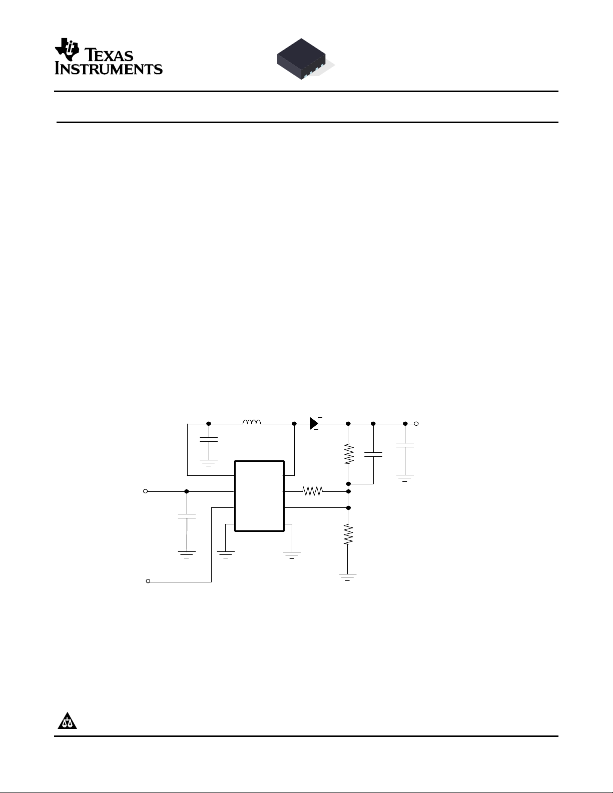
1 M
C1
100 nF
C3
L
VIN
SW
DO
FB
L1
D1
MBR0530
GND
CTRL
PGND
Enable / LCD bias control
C2
4.7uF
R2
R1
R3
Cff
22 pF
4.7 H
2.2 M
1 F
V
O
16.2 V to 18.9 V/ 10 mA
180 k
VCC = 1.8 V to 6 V
1
2
5
6
8
3
4
7
DIGITALLY ADJUSTABLE LCD BOOST CONVERTER
FEATURES DESCRIPTION
• Input Voltage Range . . . 1.8 V to 6.0 V
• Up to 85% Efficiency
• Digitally Adjustable Output Voltage Control
• Disconnects Output From Input During
Shutdown
• Switching Frequency . . . Up to 1 MHz
• No Load Quiescent Current . . . 40 µA Typ
• Thermal Shutdown Mode
• Shutdown Current . . . 0.1 µA Typ
• Available in Small 3mm × 3mm QFN package
APPLICATIONS
• LCD Bias Supply For Small to Medium LCD
Displays
• OLED Display Power Supply
– PDA, Pocket PC, Smart Phones
– Handheld Devices
– Cellular Phones
TPS61045
SLVS440A – JANUARY 2003 – REVISED SEPTEMBER 2003
The TPS61045 is a high frequency boost converter
with digitally programmable output voltage and true
shutdown. During shutdown the output is
disconnected from the input by opening the internal
input switch. This allows a controlled power up/down
sequencing of the display. The output voltage can be
increased or decreased in digital steps by applying a
logic signal to the CTRL pin. The output voltage
range, as well as the output voltage step size, can be
programmed with the feedback divider network. With
a high switching frequency of up to 1 MHz the
TPS61045 allows the use of small external
components and together, with the small 8-pin QFN
package, a minimum system solution size is
achieved.
PRODUCTION DATA information is current as of publication date.
Products conform to specifications per the terms of the Texas
Instruments standard warranty. Production processing does not
necessarily include testing of all parameters.
Figure 1. Typical Application
Copyright © 2003, Texas Instruments Incorporated
Please be aware that an important notice concerning availability, standard warranty, and use in critical applications of Texas
Instruments semiconductor products and disclaimers thereto appears at the end of this data sheet.
Page 2
www.ti.com
TPS61045
SLVS440A – JANUARY 2003 – REVISED SEPTEMBER 2003
These devices have limited built-in ESD protection. The leads should be shorted together or the device placed in conductive foam
during storage or handling to prevent electrostatic damage to the MOS gates.
ORDERING INFORMATION
T
A
8 Pin QFN Package (DRB) Package Marking
(1)
-40 °C to 85 °C TPS61045DRB BHT
(1) The DRB package is available taped and reeled. Add R suffix (TPS61045DRBR) to order quantities of 3000 units per reel. Add T suffix
(TPS61045DBRT) to order quaqntities of 250 units per reel.
ABSOLUTE MAXIMUM RATINGS
over operating free-air temperature range (unless otherwise noted)
Supply voltage, V
Voltages, V
Voltage, V
(CTRL)
(SW)
Continuous power dissipation See Dissipation Rating Table
Operating junction temperature range -40 ° C to 150 ° C
Storage temperature range, T
Lead temperature (soldering, 10 sec) 260 ° C
(1) Stresses beyond those listed under absolute maximum ratings may cause permanent damage to the device. These are stress ratings
only, and functional operation of the device at these or any other conditions beyond those indicated under recommended operating
conditions is not implied. Exposure to absolute-maximum-rated conditions for extended periods may affect device reliability.
(2) All voltage values are with respect to network ground terminal.
(2)
(VIN)
, V
, V
(FB)
(2)
(L)
(2)
, V
(DO)
STG
(1)
TPS61045
-0.3 V to 7 V
-0.3 V to VI+ 0.3 V
30 V
-65 ° C to 150 ° C
DISSIPATION RATING
PACKAGE TA≤25 °C POWER DERATING FACTOR TA= 70 °C POWER TA= 85 °C POWER
8 pin QFN (DRB)
(1)
(1) The thermal resistance junction to ambient of the 8 pin QFN package is 270 °C/W. Standard 2 layer PCB without vias for the thermal
pad. See the appliction section on how to improve the thermal resistance R
RATING ABOVE TA= 25 °C RATING RATING
370 mW 3.7 mW/ ° C 204 mW 148 mW
.
ΘJA
RECOMMENDED OPERATING CONDITIONS
MIN TYP MAX UNIT
V
(VIN)
V
(SW)
L Inductor
f Switching frequency
C
I(C2)
C
O(C3)
T
A
T
J
Input voltage range 1.8 6.0 V
Switch voltage 30 V
(1)
(1)
Input capacitor (C2)
Output capacitor (C3)
(1)
(1)
Operating ambient temperature -40 85 °C
Operating junction temperature -40 125 °C
(1) See application section for further information.
ELECTRICAL CHARACTERISTICS
VI= 2.4 V, CTRL = VI, VO= 18.0 V, IO= 10 mA, TA= -40 °C to 85 °C, typical values are at TA= 25 ° C (unless otherwise
noted)
PARAMETER TEST CONDITIONS MIN TYP MAX UNIT
Supply current
V
I
2
Input voltage range 1.8 6.0 V
Submit Documentation Feedback
4.7 µH
1 MHz
4.7 µF
1 µF
Page 3
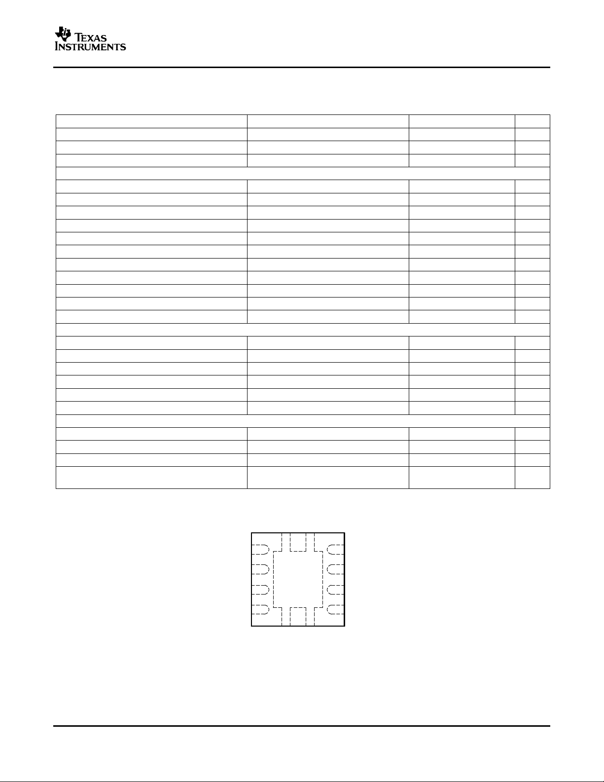
www.ti.com
SW
8
PGND7
GND6
CTRL
5
L
DRB PACKAGE
(TOP VIEW)
1
VIN 2
DO 3
FB
4
Exposed
Thermal
Die Pad
SLVS440A – JANUARY 2003 – REVISED SEPTEMBER 2003
ELECTRICAL CHARACTERISTICS (continued)
VI= 2.4 V, CTRL = VI, VO= 18.0 V, IO= 10 mA, TA= -40 °C to 85 °C, typical values are at TA= 25 ° C (unless otherwise
noted)
PARAMETER TEST CONDITIONS MIN TYP MAX UNIT
I
Q
I
O(SD)
V
UVLO
CTRL and DAC output
V
IH
V
IL
I
lkg
V
O(DO)
V
O(DO)
I
O(SINK)
t
(UP)
t
(DWN)
t
d1
t
(OFF)
Input switch (Q1), main switch (Q2) and current limit
V
SW(Q2)
r
ds(ON)
I
lkg(MAIN)
I
(LIM)
r
ds(ON)
I
lkg(IN)
Output
V
O
V
ref
I
(FB)
V
(FB)
Operating quiescent current IO= 0 mA, not switching 40 65 µA
Shutdown current CTRL = GND 0.1 1 µA
Under-voltage lockout threshold VIfalling 1.5 1.7 V
CTRL high level input voltage 1.3 V
CTRL low level input voltage 0.3 V
CTRL input leakage current CTRL = GND or VIN 0.1 µA
DAC output voltage range 0 1.233 V
DAC resolution 6 Bit 19.6 mV
DAC center output voltage CTRL = high 607 mV
Maximum DAC sink current 30 µA
Increase output voltage one step CTRL = high to low 1 60 µs
Decrease the output voltage one step CTRL = high to low 140 240 µs
Delay time between up/down steps CTRL = low to high 1 µs
Shutdown CTRL = high to low 560 µs
Main switch maximum voltage (Q2) 30 V
Main switch MOSFET on-resistance VI= 2.4 V; IS= 200 mA 400 800 m Ω
Main switch MOSFET leakage current VS= 28 V 0.1 10 µA
Main switch MOSFET current limit 300 375 450 mA
Input switch MOSFET on-resistance VI= 2.4 V; IS= 200 mA 1 2 Ω
Input switch MOSFET leakage current VL = GND, VI= 6 V 0.1 10 µA
Output voltage range Vin 28 V
Internal voltage reference 1.233 V
Feedback input bias current VFB = 1.3 V 30 100 nA
Feedback trip point voltage 1.8 V ≤ VI≤ 6.0 V; VO= 18 V, I
mA
= 10 1.208 1.233 1.258 V
(LOAD)
TPS61045
The Exposed Thermal Die Pad is connected to PGND. Connect this pad directly with the GND pin.
Submit Documentation Feedback
3
Page 4
www.ti.com
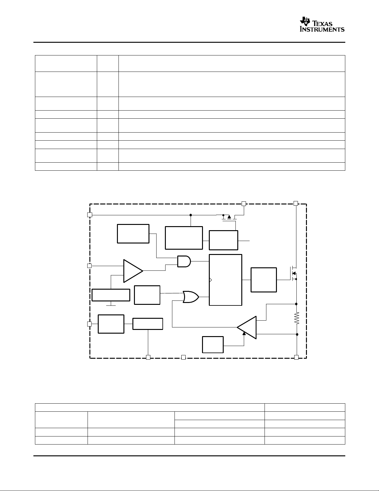
FB
PGND
SW
VIN
CTRL
+
-
Current Limit
+
-
ErrorComparator
S
R
CTRL
L
DO GND
Q1
Input switch
400 ns Min
Off Time
Undervoltage
Lockout
Bias Supply
Gate
Driver
Gate
Driver
RS Latch
Logic
6 s Max
On Time
V
ref
= 1.233 V
Digital
Interface
6 Bit DAC
Soft
Start
Q2
Main Switch
R
sense
TPS61045
SLVS440A – JANUARY 2003 – REVISED SEPTEMBER 2003
TERMINAL FUNCTIONS
TERMINAL
NAME NO.
CTRL 5 I Combined enable and digital output voltage programming pin. Pulling CTRL constantly high enables
DO 3 O Internal DAC output. DO programs the output voltage via the CTRL pin. Refer to the application
FB 4 I Feedback. FB must be connected to the output voltage-feedback divider.
GND 7 Analog ground. GND must be directly connected to the PGND pin. Refer to the application
L 1 O Drain of the internal switch (Q1). Connect L to the inductor.
PGND 6 Power ground
SW 8 I Drain of the integrated switch Q2. SW is connected to the inductor and anode of the Schottky
VIN 2 I Input supply pin
I/O DESCRIPTION
the device. When CTRL is pulled to GND, the device is disabled and the input is disconnected from
the output by opening the integrated switch Q1. Pulsing CTRL low increases or decreases the output
voltage. Refer to the application information section for further information.
information section for further information.
information section for further information.
rectifier diode.
FUNCTIONAL BLOCK DIAGRAM
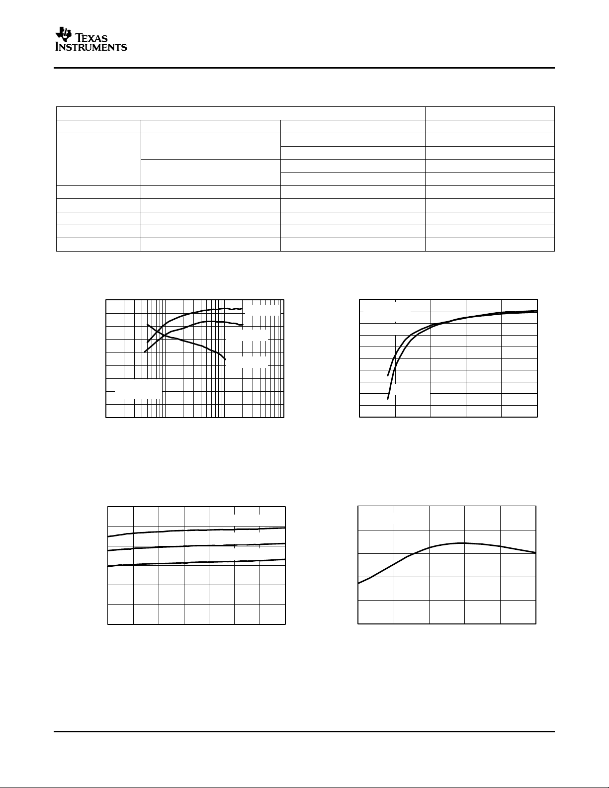
η Efficiency vs Load current Figure 2
I
DD(Q)
V
(FB)
4
Quiescent current vs Input voltage Figure 4
Feedback voltage vs Temperature Figure 5
Typical Characteristics
Submit Documentation Feedback
Table of Graphs
vs Input voltage Figure 3
FIGURE
Page 5
www.ti.com
IO - Output Current - mA
70
72
74
76
78
80
82
84
86
88
L = 4.7 µH
VO = 18 V
0.1 1 10 100
Efficiency - %
VI = 5 V
VI = 3.6 V
VI = 2.4 V
VI - Input Voltage - V
60
63
66
69
72
75
78
81
84
87
90
1 2 3 4 5 6
Efficiency - %
IO = 10 mA
IO = 5 mA
L = 4.7 µH
VO = 18 V
TA - Free-Air Temperature - °C
1.233
1.234
1.235
1.236
1.237
1.238
-40 -15 10 35 60 85
V
(fb)
- Feedback Voltage - V
VI = 2.4 V
VI - Input Voltage - V
0
10
20
30
40
50
60
1.8 2.4 3.0 3.6 4.2 4.8 5.4 6.0
I
DD(Q)
- Quiescent Current - µA
TA = -40°C
TA = 25°C
TA = 85°C
TPS61045
SLVS440A – JANUARY 2003 – REVISED SEPTEMBER 2003
Typical Characteristics (continued)
Table of Graphs (continued)
FIGURE
I
(FB)
r
ds(on)
V
(DO)
Feedback current vs Temperature Figure 6
r
Main switch Q2 vs Temperature Figure 7
ds(on)
vs Input voltage Figure 8
r
Input switch Q1 vs Temperature Figure 9
ds(on)
vs Input voltage Figure 10
V
Voltage vs CTRL input step Figure 11
(DO)
Line transient response Figure 12
Load transient response Figure 13
PFM operation Figure 14
Soft start Figure 15
Efficiency Efficiency
vs vs
Load Current Input Voltage
Quiescent Current Feedback Voltage
Figure 2. Figure 3.
vs vs
Input Voltage Temperature
Figure 4. Figure 5.
Submit Documentation Feedback
5
Page 6
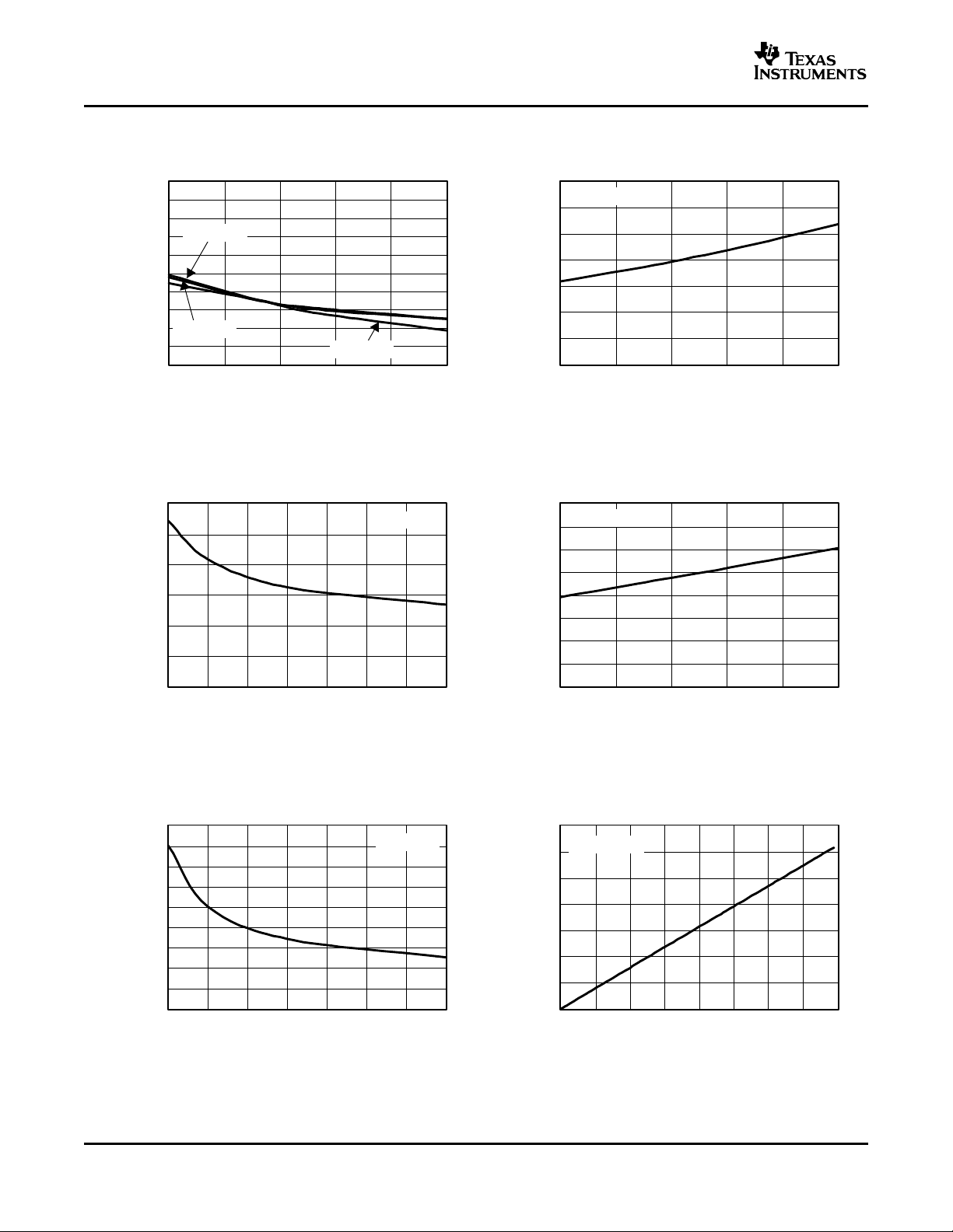
www.ti.com
0
10
20
30
40
50
60
70
80
90
100
-40 -15 10 35 60 85
TA - Free-Air Temperature - °C
I
(fb)
- Feedback Current - nA
VI = 5 V
VI = 3.6 V
VI = 2.4 V
0
100
200
300
400
500
600
700
-40 -15 10 35 60 85
TA - Free-Air Temperature - °C
r
ds(on)
- On-State Resistance - MΩ
VI = 2.4 V
0
100
200
300
400
500
600
1.8 2.4 3.0 3.6 4.2 4.8 5.4 6.0
VI - Input Voltage - V
r
ds(on)
- On-State Resistance - MΩ
TA = 25°C
0.0
0.2
0.4
0.6
0.8
1.0
1.2
1.4
1.6
-40 -15 10 35 60 85
TA - Free-Air Temperature - °C
r
ds(on)
- On-State Resistance - Ω
VI = 2.4 V
0.0
0.2
0.4
0.6
0.8
1.0
1.2
1.4
1.6
1.8
1.8 2.4 3.0 3.6 4.2 4.8 5.4 6.0
VI - Input Voltage - V
r
ds(on)
- On-State Resistance - Ω
TA = 25°C
0.0
0.2
0.4
0.6
0.8
1.0
1.2
1.4
0 8 16 24 32 40 48 56 64
Input Step Number
V
(DO)
– Drop–Out Voltage – V
VI = 2.4 V
TPS61045
SLVS440A – JANUARY 2003 – REVISED SEPTEMBER 2003
Feedback Current r
vs vs
Temperature Temperature
Figure 6. Figure 7.
r
Main Switch Q2 r
ds(ON)
vs vs
Input Voltage Temperature
ds(ON)
ds(ON)
Main Switch Q2
Input Switch Q1
r
ds(ON)
6
Figure 8. Figure 9.
Input Switch Q1 V
vs vs
(DO)
Input Voltage CTRL Input Step
Figure 10. Figure 11.
Submit Documentation Feedback
Voltage
Page 7
www.ti.com
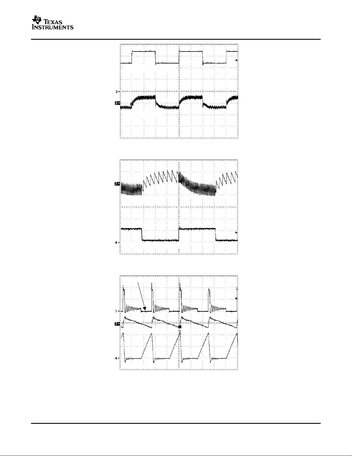
250 µs/Div
VI = 2.4 V to 3.4 V Step
VO = 100 mV/Div
I
(Load)
= 1 mA to 11 mA Step
VO = 50 mV/Div
50 µs/Div
VO = 50 mV/Div
1 µs/Div
V
(SW)
= 10 V/Div
IL = 200 mA/Div
Figure 12. . Line Transient Response
TPS61045
SLVS440A – JANUARY 2003 – REVISED SEPTEMBER 2003
Figure 13. . Load Transient Response
Figure 14. . PFM Operation
Submit Documentation Feedback
7
Page 8

www.ti.com
500 µs/Div
II = 50 mA/Div
CTRL 2 V/Div
VO = 5 V/Div
I
P(typ)
I
(LIM)
V
I
L
100 ns
I
P(typ)
400 mA
V
I
L
100 ns
TPS61045
SLVS440A – JANUARY 2003 – REVISED SEPTEMBER 2003
Figure 15. . Soft Start
DETAILED DESCRIPTION
OPERATION
The TPS61045 operates with an input voltage range of 1.8 V to 6.0 V and generates output voltages up to 28 V.
The device operates in a pulse frequency modulation (PFM) scheme with constant peak current control. This
control scheme maintains high efficiency over the entire load current range and, with a switching frequency of up
to 1 MHz, the device enables the use of small external components.
The converter monitors the output voltage and when the feedback voltage falls below the reference voltage of
1.233 V (typ) the main switch turns on and the current ramps up. The main switch turns off when the inductor
current reaches the internally set peak current of 375 mA (typ). Refer to the peak current controlsection for more
information. The second criteria that turns off the main switch is the maximum on-time of 6 µs (typ). This limits
the maximum on-time of the converter in extreme conditions. As the switch is turned off, the external Schottky
diode is forward biased delivering the current to the output. The main switch remains off until the minimum off
time of 400 ns (typ) has passed and the feedback voltage is below the reference voltage again. Using this PFM
peak current control scheme, the converter operates in discontinuous conduction mode (DCM) where the
switching frequency depends on the input voltage, output voltage and output current. This gives a high efficiency
over the entire load current range. This regulation scheme is inherently stable which allows a wider range for the
selection of the inductor and output capacitor.
PEAK CURRENT CONTROL
The internal switch is turned on until the inductor current reaches the typical dc current limit (I
Due to the internal current limit delay of 100 ns (typ) the actual current exceeds the dc current limit threshold by
a small amount. The typical peak current limit can be calculated:
The higher the input voltage and the lower the inductor value, the greater the current limit overshoot.
SOFTSTART
All inductive step-up converters exhibit high inrush current during start up if no special precautions are taken.
This can cause voltage drops at the input rail during start-up, which may result in an unwanted or premature
system shut down.
8
Submit Documentation Feedback
LIM
) of 375 mA.
Page 9

www.ti.com
V
O(DO)
V
ref
26–1
TPS61045
SLVS440A – JANUARY 2003 – REVISED SEPTEMBER 2003
DETAILED DESCRIPTION (continued)
When the device is enabled, the internal input switch (Q1) is slowly turned on to reduce the in-rush current
charging the capacitor (C2) connected to pin L. Furthermore, the TPS61045 limits this in-rush current during
start-up by increasing the current limit in two steps starting from I
256 switch cycles.
ENABLE (CTRL PIN)
The CTRL pin serves two functions. One is the enable and disable of the device. The other is the output voltage
programming of the device. If the digital interface is not required, the CTRL pin is used as a standard enable pin
for the device.
Pulling the CTRL pin high enables the device beginning with the softstart cycle.
Pulling the CTRL pin to ground for a period of ≥ 560 µs shuts down the device, reducing the shutdown current to
0.1 µA (typ). During shutdown the internal input switch (Q1) remains open and disconnects the load from the
input supply of the device.
This pin must be terminated.
DAC OUTPUT (DO)
The TPS61045 allows digital adjustment of the output voltage using the digital CTRL interface as described in
the next section. The DAC output pin (DO) drives an external resistor (R3) connected to the external feedback
divider. The DO output has a typical output voltage range from 0 V to V
set to 0 V, the external resistor (R3) is more or less in parallel to the lower feedback resistor (R2) giving the
highest output voltage. Programming the DO output to V
DAC is used with 64-steps and 0 as the first step. This gives a typical voltage step of 19.6 mV which is
calculated as:
ref
/4 for 256 switch cycles to I
LIM
(1.233V). If the DO output voltage is
ref
gives the lowest output voltage. Internally, a 6-bit
LIM
/2 for the next
See the section setting the output voltage for further information.
After start-up, when the CTRL pin is pulled high, the DO output voltage is set to its center voltage which is the
32nd step of typically V
= 607mV.
(DO)
DIGITAL INTERFACE (CTRL)
When the CTRL pin is pulled high the device starts up with softstart and the DAC output voltage (DO) sets to its
center voltage with a typical output voltage of 607 mV.
The output voltage can be programmed by pulling the CTRL pin low for a certain period of time. Depending on
this time period the internal DAC voltage increases or decreases one digital step, as outlined in Table 1 and
Figure 16 . Programming the DAC output V
output voltage. If the DAC is programmed to its maximum output voltage equal to the internal reference voltage,
typically V
=1.233 V, then the output has its minimum output voltage.
(DO)
to 0 V places R3 in parallel to R2, which gives the maximum
(DO)
Submit Documentation Feedback
9
Page 10

www.ti.com
t
d1
t
(DWN)
t
d1
t
(OFF)
Device Enabled Device Disabled
High
Low
EN
t
d1
t
(UP)
TPS61045
SLVS440A – JANUARY 2003 – REVISED SEPTEMBER 2003
DETAILED DESCRIPTION (continued)
Table 1. Timing Table
DAC OUTPUT DO TIME LOGIC LEVEL
Increase one step t
Decrease one step t
Shutdown t
Delay between steps td1= 1 µs High
= 1 µs to 60 µs Low
(UP)
= 140 µs to 240 µs Low
(DWN)
≥ 560 µs Low
(OFF)
Figure 16. CTRL Timing Diagram
UNDERVOLTAGE LOCKOUT
An undervoltage lockout feature prevents misoperation of the device at input voltages below 1.5 V (typ). As long
as the input voltage is below the undervoltage threshold the device remains off, with the input switch (Q1) and
the main switch (Q2) open.
THERMAL SHUTDOWN
An internal thermal shutdown is implemented in the TPS61045 that shuts down the device if the typical junction
temperature of 160 °C is exceeded. If the device is in thermal shutdown mode, the input switch (Q1) and the
main switch (Q2) are open.
10
Submit Documentation Feedback
Page 11

www.ti.com
f
s
(max)
V
I
VO V
I
IP L V
O
I
P(typ)
375 mA
V
I
L
100 ns
f
s
(ILOAD)
2 I
LOAD
VO–VI V
F
I
2
P
L
I
P(typ)
375 mA
V
I
L
100 ns
TPS61045
SLVS440A – JANUARY 2003 – REVISED SEPTEMBER 2003
APPLICATION INFORMATION
INDUCTOR SELECTION, MAXIMUM LOAD CURRENT
Since the PFM peak current control scheme is inherently stable the inductor and capacitor value does not affect
the stability of the regulator. The selection of the inductor together with the nominal load current, input, and
output voltage of the application determines the switching frequency of the converter. Depending on the
application, inductor values between 2.2 µH up to 47 µH are recommended. The maximum inductor value is
determined by the maximum switch on-time of 6 µs (typ). The peak current limit of 375 mA (typ) must be
reached within this 6 µs for proper operation.
The inductor value determines the maximum switching frequency of the converter. Therefore, the inductor value
must be selected for the maximum switching frequency, at maximum load current of the converter and should
not be exceeded. A good inductor value to start with is 4.7 µH. The maximum switching frequency is calculated
as:
with:
IP= peak current as described in the previous peak current control section.
L = selected inductor value
If the selected inductor does not exceed the maximum switching frequency of the converter, as a next step, the
switching frequency at the nominal load current is estimated as follows:
with:
IP= peak current as described in the previous chapter peak current control section
L = selected inductor value
I
= nominal load current
(LOAD)
V
= rectifier diode forward voltage (typically 0.3 V)
F
The smaller the inductor value, the higher the switching frequency of the converter but the lower the efficiency.
The maximum load current of the converter is determined at the operation point where the converter starts to
enter continuous conduction mode. The converter must always operate in discontinuous conduction mode to
maintain regulation.
Two conditions exist for determining the maximum output current of the converter. One is when the inductor
current fall time is <400 ns, and the other is when the inductor current fall time is >400 ns.
One way to calculate the maximum available load current under certain operation conditions is to estimate the
expected converter efficiency at the maximum load current. This number can be taken out of the efficiency
graphs shown in Figure 2 and Figure 3. Then the maximum load current can be estimated:
Inductor fall time:
Submit Documentation Feedback
11
Page 12
www.ti.com
t
fall
IP L
VO–V
I
I
load max
IP V
I
2 V
O
I
load max
I
2
P
L V
I
VO–V
I
2 IP L 2 400 ns V
I
IP 300 mA
V
I
2
100 ns
V
O(min)
V
(FB)
R1
R2
1
V
O(max)
V
(FB)
R1
R3
V
(FB)
R1
R2
1
TPS61045
SLVS440A – JANUARY 2003 – REVISED SEPTEMBER 2003
APPLICATION INFORMATION (continued)
For tf≥ 400 ns
tf≤ 400 ns
with:
L = selected inductor value
η = expected converter efficiency (typically between 70% to 85%)
IP= peak current as described in the previous peak current control section.
The above formula contains the expected converter efficiency that allows calculating the expected maximum
load current the converter can support. The efficiency can be taken out of the efficiency graphs shown in Figures
2 and 3 or 80% can be used as a good estimation.
The selected inductor must have a saturation current which meets the maximum peak current of the converter
as calculated in the peak current control section. Use the maximum value for I
Another important inductor parameter is the dc resistance. The lower the dc resistance, the higher the efficiency
of the converter. Refer to the Table 1 and the inductor selection section under typical applications.
Table 2. Possible Inductor Selection
INDUCTOR VALUE COMPONENT SUPPLIER COMMENTS
10 µH Sumida CR32-100 High efficiency
10 µH Sumida CDRH3D16-100 High efficiency
10 µH Murata LQH43CN100K01
4.7 µH Sumida CDRH3D16-4R7 Small solution size
4.7 µH muRata LQH32CN4R7M51 Small solution size
Lim
(450mA) for this calculation.
SETTING THE OUTPUT VOLTAGE
When the converter is programmed to the minimum output voltage, the DAC output (DO) equals the reference
voltage of 1.233 V (typ). Therefore, only the feedback resistor network (R1) and (R2) determines the output
voltage under these conditions. This gives the minimum output voltage possible and can be calculated as:
The maximum output voltage is determined as the DAC output (DO) is set to 0 V:
The output voltage can be digitally programmed by pulling the CTRL pin low for a certain period of time as
described in the Digital Interface section. Pulling the signal applied to the CTRL pin low increases or decreases
the DAC output DO (pin 3) one-step where one step is typically 19.6 mV. A voltage step on DO of 19.6mV (typ)
changes the output voltage by one step and is calculated as:
12
Submit Documentation Feedback
Page 13

www.ti.com
V
O(step)
19.6 mV R1
R3
VO 1.233 V1
R1
R2
C
FF
1
2
f
s
20
R1
V
O
I
O
C
O
1
f
s(ILOAD)
IP L
VO VF V
I
IP ESR
IP 375 mA
V
I
2
100 ns
TPS61045
SLVS440A – JANUARY 2003 – REVISED SEPTEMBER 2003
The possible output voltage range is determined by selecting R1, R2 and R3. A possible larger output voltage
range gives a larger output voltage step size. The smaller the possible output voltage range, the smaller the
output voltage step size.
To reduce the overall operating quiescent current in battery powered applications a high impedance voltage
divider must be used with a typical value for R2 of ≤ 200 k Ω and a maximum value for R1 of 2.2 M Ω.
Some applications may not need the digital interface to program the output voltage. In this case the output DO
can be left open as shown in Figure 18 and the output voltage is calculated as for any standard boost converter:
In such a configuration a high impedance voltage divider must also be used to minimize ground current and a
typical value for R2 of ≤ 200 k Ω and a maximum value for R1 of 2.2 M Ω are recommended.
A feed-forward capacitor (C
overdrive for the error comparator. Without a feed-forward capacitor or a too small feed-forward capacitor value,
the device shows double pulses or a pulse burst instead of single pulses at the switch node (SW). This can
cause higher output voltage ripple. If a higher output voltage ripple is acceptable, the feedforward capacitor can
be left out too.
The lower the switching frequency of the converter, the larger the feed-forward capacitor value needs to be. A
good starting point is the use of a 10 pF feed-forward capacitor. As a first estimation, the required value for the
feed-forward capacitor can be calculated at the operation point:
), across the upper feedback resistor (R1), is required to provide sufficient
(FF)
with:
R1 = upper resistor of voltage divider
fS= switching frequency of the converter at the nominal load current. (For the calculation of the switching
frequency see previous section)
For C
The larger the feed-forward capacitor, the worse the line regulation of the device. Therefore, the feed-forward
capacitor must be selected as small as possible if good line regulation is of concern.
choose a value which comes closest to the calculation result.
(FF)
OUTPUT CAPACITOR SELECTION
For better output voltage filtering a low ESR output capacitor is recommended. Ceramic capacitors have low
ESR values but depending on the application, tantalum capacitors can also be used. Refer to Table 2 and
typical applications for the selection of the output capacitor.
Assuming the converter does not show double pulses or pulse bursts on the switch node (SW) the output
voltage ripple is calculated as:
with:
IP= peak current as described in the previous section peak current control
L = selected inductor value
I
O(LOAD)
=Nominal load current
Submit Documentation Feedback
13
Page 14

www.ti.com
TPS61045
SLVS440A – JANUARY 2003 – REVISED SEPTEMBER 2003
f
V
C
= switching frequency at the nominal load current as calaculated previously.
S(ILoad)
= rectifier diode forward voltage (typically 0.3 V)
F
= selected output capacitor
O
ESR = output capacitor ESR value
INPUT CAPACITOR SELECTION
The input capacitor (C1) filters the high frequency noise to the control circuit and must be directly connected to
the input pin (VIN) of the device. The capacitor (C2) connected to the L pin of the device is the input capacitor
for the power stage.
The main purpose of the capacitor (C2), that is connected directly to the L pin, is to smooth the inductor current.
A larger capacitor reduces the inductor ripple current present at the L pin. The smaller the ripple current at the L
pin, the higher the efficiency of the converter. If a sufficiently large capacitor is used, the input switch must carry
only the DC current, filtered by the capacitor (C2), and not the high switching currents of the converter. A 4.7 µF
or 10- µF ceramic capacitor (C2) is sufficient for most applications. For better filtering, this value can be
increased without limit. Refer to Table 2 and typical applications for input capacitor recommendations.
Table 3. Possible Input and Output Capacitor Selection
CAPACITOR VOLTAGE RATING COMPONENT SUPPLIER COMMENTS
4.7 F/X5R/0805 6.3 V Tayo Yuden JMK212BY475MG CI/C
10 µF/X5R/0805 6.3 V Tayo Yuden JMK212BJ106MG CI/C
1.0 µF/X7R/1206 25 V Tayo Yuden TMK316BJ105KL C
1.0 µF/X7R/1206 35 V Tayo Yuden GMK316BJ105KL C
4.7 µF/X5R/1210 25 V Tayo Yuden TMK325BJ475MG C
O
O
O
O
O
DIODE SELECTION
To achieve high efficiency a Schottky diode must be used. The current rating of the diode must meet the peak
current rating of the converter as it is calculated in the peak current control section. Use the maximum value for
I
(450mA) for this calculation. Refer to Table 3 and the typical applications for the selection of the Schottky
(LIM)
diode.
14
Submit Documentation Feedback
Page 15

www.ti.com
L1
4.7 µH
LQH32CN4R7M11
Enable / LCD
Bias Control
L
SW
DO
FB
GND
CTRL
PGND
VCC = 1.8 V to 6 V
C2
4.7 µF
D1
Zetex ZHZS400
Vin
R3
1 M
R1
2.2 M
Cff
22 pF
V
O
16.2 V to 18.9 V/ 10 mA
R2
180 kΩ
C1
100 nF
C3
1 µF
TPS61045
SLVS440A – JANUARY 2003 – REVISED SEPTEMBER 2003
Table 4. Possible Schottky Diode Selection
COMPONENT SUPPLIER REVERSE VOLTAGE
ON Semiconductor MBR0530 30 V
ON Semiconductor MBR0520 20 V
ON Semiconductor MBRM120L 20 V
Toshiba CRS02 30 V
Zetex CHZS400 40 V
LAYOUT CONSIDERATIONS
As for all switching power supplies the layout is an important step in the design, especially at high peak currents
and switching frequencies. If the layout is not carefully implemented the regulator can show noise problems and
duty cycle jitter.
The input capacitor must be placed as close as possible to the input pin for good input-voltage filtering. The
inductor and diode must be placed as close as possible to the switch pin (SW) to minimize noise coupling into
other circuits. Since the feedback pin and network is a high impedance circuit, the feedback network must be
routed away from the inductor.
THERMAL CONSIDERATIONS
The TPS61045 is available in a thermally enhanced QFN package. The package includes a thermal pad,
improving the thermal capabilities of the package. See QFN/SON PCB attachment application note (SLUA271).
The thermal resistance junction to ambient (R
thermal vias and wide PCB, traces improve thermal resistance (R
PCB vias are required for the thermal pad. However, the thermal pad must be soldered to the PCB.
) of the QFN package depends on the PCB layout. By using
ΘJA
). Under normal operation conditions no
ΘJA
TYPICAL APPLICATIONS
Figure 17. Typical Application With Digital Adjusted Output Voltage
Submit Documentation Feedback
15
Page 16

www.ti.com
L1
4.7 µH
LQH32CN4R7M11
Enable
L
SW
DO
FB
GND
CTRL
PGND
VCC = 1.8 V to 6 V
C2
4.7 µF
D1
Zetex ZHZS400
Vin
R1
2.2 M
Cff
22 pF
V
O
15 V to 18 V
Adjustable / 10 mA
R2
160 kΩ
C1
100 nF
C3
1 µF
R3
390 kΩ
DAC or Analog Voltage
0 V = 25 V
1.233 V = 18 V
L1
4.7 µH
LQH32CN4R7M23
L
SW
DO
FB
GND
CTRL
PGND
VCC = 2.7 V to 6 V
C2
4.7 µF
D1
Zetex ZHZS400
Vin
R1
2.2 M
Cff
22 pF
V
O
16.2 V to 18.9 V/
20 mA
R2
180 kΩ
C1
100 nF
C3
1 µF
Enable / LCD
Bias Control
R3
1 M
TPS61045
SLVS440A – JANUARY 2003 – REVISED SEPTEMBER 2003
Figure 18. Typical Application With Analog Adjusted Output Voltage
TYPICAL APPLICATIONS (continued)
16
Figure 19. OLED Supply Providing Higher Output Current
Submit Documentation Feedback
Page 17

PACKAGE OPTION ADDENDUM
www.ti.com
18-Jul-2006
PACKAGING INFORMATION
Orderable Device Status
(1)
Package
Type
Package
Drawing
Pins Package
Qty
Eco Plan
TPS61045DRBR ACTIVE SON DRB 8 3000 Green (RoHS &
no Sb/Br)
TPS61045DRBRG4 ACTIVE SON DRB 8 3000 Green (RoHS &
no Sb/Br)
TPS61045DRBT ACTIVE SON DRB 8 250 Green (RoHS &
no Sb/Br)
TPS61045DRBTG4 ACTIVE SON DRB 8 250 Green (RoHS &
no Sb/Br)
(1)
The marketing status values are defined as follows:
ACTIVE: Product device recommended for new designs.
LIFEBUY: TI has announced that the device will be discontinued, and a lifetime-buy period is in effect.
NRND: Not recommended for new designs. Device is in production to support existing customers, but TI does not recommend using this part in
a new design.
PREVIEW: Device has been announced but is not in production. Samples may or may not be available.
OBSOLETE: TI has discontinued the production of the device.
(2)
Eco Plan - The planned eco-friendly classification: Pb-Free (RoHS), Pb-Free (RoHS Exempt), or Green (RoHS & no Sb/Br) - please check
http://www.ti.com/productcontent for the latest availability information and additional product content details.
TBD: The Pb-Free/Green conversion plan has not been defined.
Pb-Free (RoHS): TI's terms "Lead-Free" or "Pb-Free" mean semiconductor products that are compatible with the current RoHS requirements
for all 6 substances, including the requirement that lead not exceed 0.1% by weight in homogeneous materials. Where designed to be soldered
at high temperatures, TI Pb-Free products are suitable for use in specified lead-free processes.
Pb-Free (RoHS Exempt): This component has a RoHS exemption for either 1) lead-based flip-chip solder bumps used between the die and
package, or 2) lead-based die adhesive used between the die and leadframe. The component is otherwise considered Pb-Free (RoHS
compatible) as defined above.
Green (RoHS & no Sb/Br): TI defines "Green" to mean Pb-Free (RoHS compatible), and free of Bromine (Br) and Antimony (Sb) based flame
retardants (Br or Sb do not exceed 0.1% by weight in homogeneous material)
(2)
Lead/Ball Finish MSL Peak Temp
CU NIPDAU Level-2-260C-1 YEAR
CU NIPDAU Level-2-260C-1 YEAR
CU NIPDAU Level-2-260C-1 YEAR
CU NIPDAU Level-2-260C-1 YEAR
(3)
(3)
MSL, Peak Temp. -- The Moisture Sensitivity Level rating according to the JEDEC industry standard classifications, and peak solder
temperature.
Important Information and Disclaimer:The information provided on this page represents TI's knowledge and belief as of the date that it is
provided. TI bases its knowledge and belief on information provided by third parties, and makes no representation or warranty as to the
accuracy of such information. Efforts are underway to better integrate information from third parties. TI has taken and continues to take
reasonable steps to provide representative and accurate information but may not have conducted destructive testing or chemical analysis on
incoming materials and chemicals. TI and TI suppliers consider certain information to be proprietary, and thus CAS numbers and other limited
information may not be available for release.
In no event shall TI's liability arising out of such information exceed the total purchase price of the TI part(s) at issue in this document sold by TI
to Customer on an annual basis.
Addendum-Page 1
Page 18

Page 19

Page 20

Page 21

IMPORTANT NOTICE
Texas Instruments Incorporated and its subsidiaries (TI) reserve the right to make corrections, modifications,
enhancements, improvements, and other changes to its products and services at any time and to discontinue
any product or service without notice. Customers should obtain the latest relevant information before placing
orders and should verify that such information is current and complete. All products are sold subject to TI’s terms
and conditions of sale supplied at the time of order acknowledgment.
TI warrants performance of its hardware products to the specifications applicable at the time of sale in
accordance with TI’s standard warranty. Testing and other quality control techniques are used to the extent TI
deems necessary to support this warranty . Except where mandated by government requirements, testing of all
parameters of each product is not necessarily performed.
TI assumes no liability for applications assistance or customer product design. Customers are responsible for
their products and applications using TI components. To minimize the risks associated with customer products
and applications, customers should provide adequate design and operating safeguards.
TI does not warrant or represent that any license, either express or implied, is granted under any TI patent right,
copyright, mask work right, or other TI intellectual property right relating to any combination, machine, or process
in which TI products or services are used. Information published by TI regarding third-party products or services
does not constitute a license from TI to use such products or services or a warranty or endorsement thereof.
Use of such information may require a license from a third party under the patents or other intellectual property
of the third party, or a license from TI under the patents or other intellectual property of TI.
Reproduction of information in TI data books or data sheets is permissible only if reproduction is without
alteration and is accompanied by all associated warranties, conditions, limitations, and notices. Reproduction
of this information with alteration is an unfair and deceptive business practice. TI is not responsible or liable for
such altered documentation.
Resale of TI products or services with statements different from or beyond the parameters stated by TI for that
product or service voids all express and any implied warranties for the associated TI product or service and
is an unfair and deceptive business practice. TI is not responsible or liable for any such statements.
Following are URLs where you can obtain information on other Texas Instruments products and application
solutions:
Products Applications
Amplifiers amplifier.ti.com Audio www.ti.com/audio
Data Converters dataconverter.ti.com Automotive www.ti.com/automotive
DSP dsp.ti.com Broadband www.ti.com/broadband
Interface interface.ti.com Digital Control www.ti.com/digitalcontrol
Logic logic.ti.com Military www.ti.com/military
Power Mgmt power.ti.com Optical Networking www.ti.com/opticalnetwork
Microcontrollers microcontroller.ti.com Security www.ti.com/security
Low Power Wireless www.ti.com/lpw Telephony www.ti.com/telephony
Video & Imaging www.ti.com/video
Wireless www.ti.com/wireless
Mailing Address: Texas Instruments
Post Office Box 655303 Dallas, Texas 75265
Copyright 2006, Texas Instruments Incorporated
 Loading...