

Page 1

User’s Guide
February 2002
PMP Portable Power
SLVU065
Page 2

IMPORTANT NOTICE
Texas Instruments Incorporated and its subsidiaries (TI) reserve the right to make corrections, modifications,
enhancements, improvements, and other changes to its products and services at any time and to discontinue
any product or service without notice. Customers should obtain the latest relevant information before placing
orders and should verify that such information is current and complete. All products are sold subject to TI’s terms
and conditions of sale supplied at the time of order acknowledgment.
TI warrants performance of its hardware products to the specifications applicable at the time of sale in
accordance with TI’s standard warranty. Testing and other quality control techniques are used to the extent TI
deems necessary to support this warranty . Except where mandated by government requirements, testing of all
parameters of each product is not necessarily performed.
TI assumes no liability for applications assistance or customer product design. Customers are responsible for
their products and applications using TI components. To minimize the risks associated with customer products
and applications, customers should provide adequate design and operating safeguards.
TI does not warrant or represent that any license, either express or implied, is granted under any TI patent right,
copyright, mask work right, or other TI intellectual property right relating to any combination, machine, or process
in which TI products or services are used. Information published by TI regarding third−party products or services
does not constitute a license from TI to use such products or services or a warranty or endorsement thereof.
Use of such information may require a license from a third party under the patents or other intellectual property
of the third party, or a license from TI under the patents or other intellectual property of TI.
Reproduction of information in TI data books or data sheets is permissible only if reproduction is without
alteration and is accompanied by all associated warranties, conditions, limitations, and notices. Reproduction
of this information with alteration is an unfair and deceptive business practice. TI is not responsible or liable for
such altered documentation.
Resale of TI products or services with statements different from or beyond the parameters stated by TI for that
product or service voids all express and any implied warranties for the associated TI product or service and
is an unfair and deceptive business practice. TI is not responsible or liable for any such statements.
Mailing Address:
Texas Instruments
Post Office Box 655303
Dallas, Texas 75265
Copyright 2002, Texas Instruments Incorporated
Page 3

EVM IMPORTANT NOTICE
Texas Instruments (TI) provides the enclosed product(s) under the following conditions:
This evaluation kit being sold by TI is intended for use for ENGINEERING DEVELOPMENT OR EVALUATION
PURPOSES ONLY and is not considered by TI to be fit for commercial use. As such, the goods being provided
may not be complete in terms of required design-, marketing-, and/or manufacturing-related protective
considerations, including product safety measures typically found in the end product incorporating the goods.
As a prototype, this product does not fall within the scope of the European Union directive on electromagnetic
compatibility and therefore may not meet the technical requirements of the directive.
Should this evaluation kit not meet the specifications indicated in the EVM User’s Guide, the kit may be returned
within 30 days from the date of delivery for a full refund. THE FOREGOING WARRANTY IS THE EXCLUSIVE
WARRANTY MADE BY SELLER TO BUYER AND IS IN LIEU OF ALL OTHER WARRANTIES, EXPRESSED,
IMPLIED, OR S TATUTORY, INCLUDING ANY WARRANTY OF MERCHANTABILITY OR FITNESS FOR ANY
PARTICULAR PURPOSE.
The user assumes all responsibility and liability for proper and safe handling of the goods. Further, the user
indemnifies TI from all claims arising from the handling or use of the goods. Please be aware that the products
received may not be regulatory compliant or agency certified (FCC, UL, CE, etc.). Due to the open construction
of the product, it is the user’s responsibility to take any and all appropriate precautions with regard to electrostatic
discharge.
EXCEPT TO THE EXTENT OF THE INDEMNITY SET FORTH ABOVE, NEITHER PARTY SHALL BE LIABLE
TO THE OTHER FOR ANY INDIRECT, SPECIAL, INCIDENTAL, OR CONSEQUENTIAL DAMAGES.
TI currently deals with a variety of customers for products, and therefore our arrangement with the user is not
exclusive.
TI assumes no liability for applications assistance, customer product design, software performance, or
infringement of patents or services described herein.
Please read the EVM User’s Guide and, specifically, the EVM Warnings and Restrictions notice in the EVM
User’s Guide prior to handling the product. This notice contains important safety information about temperatures
and voltages. For further safety concerns, please contact the TI application engineer.
Persons handling the product must have electronics training and observe good laboratory practice standards.
No license is granted under any patent right or other intellectual property right of TI covering or relating to any
machine, process, or combination in which such TI products or services might be or are used.
Mailing Address:
Texas Instruments
Post Office Box 655303
Dallas, Texas 75265
Copyright 2002, Texas Instruments Incorporated
Page 4

EVM WARNINGS AND RESTRICTIONS
It is important to operate this EVM within the supply voltage range of 1.8 V to 6 V.
Exceeding the specified supply range may cause unexpected operation and/or irreversible
damage to the EVM. If there are questions concerning the supply range, please contact a TI
field representative prior to connecting the input power.
Applying loads outside of the specified output range may result in unintended operation and/or
possible permanent damage to the EVM. Please consult the EVM User’s Guide prior to
connecting any load to the EVM output. If there is uncertainty as to the load specification,
please contact a TI field representative.
During normal operation, some circuit components may have case temperatures greater than
125°C. The EVM is designed to operate properly with certain components above 125°C as
long as the input and output ranges are maintained. These components include but are not
limited to linear regulators, switching transistors, pass transistors, and current sense
resistors. These types of devices can be identified using the EVM schematic located in the
EVM User’s Guide. When placing measurement probes near these devices during operation,
please be aware that these devices may be very warm to the touch.
Mailing Address:
Texas Instruments
Post Office Box 655303
Dallas, Texas 75265
Copyright 2002, Texas Instruments Incorporated
Page 5

About This Manual
This users guide describes the characteristics, operation, and use of the
TPS61040EVM LCD bias supply evaluation module (EVM). This EVM is a
Texas Instruments high-efficiency boost converter that is configured to
generate 18 V at 2 0 mA, for LCD bias supply, from a single cell Li−Ion battery.
The users guide includes a schematic diagram, bill of materials (BOM), and
test data.
How to Use This Manual
This document contains the following chapters:
- Chapter 1—Introduction
- Chapter 2—Setup and Test Results
- Chapter 3—Board Layout
- Chapter 4—Schematic and Bill of Materials
Related Documentation From Texas Instruments
- TPS601040/41 data sheet (literature number SLVS413).
FCC Warning
This equipment is intended for use in a laboratory test environment only. It
generates, uses, and can radiate radio frequency energy and has not been
tested for compliance with the limits of computing devices pursuant to subpart
J of part 15 of FCC rules, which are designed to provide reasonable protection
against radio frequency interference. Operation of this equipment in other
environments may cause interference with radio communications, in which
case the user at his own expense will be required to take whatever measures
may be required to correct this interference.
Read This First
v
Page 6

vi
Page 7

Running Title—Attribute Reference
1 Introduction 1-1. . . . . . . . . . . . . . . . . . . . . . . . . . . . . . . . . . . . . . . . . . . . . . . . . . . . . . . . . . . . . . . . . . . . .
1.1 Background 1-2. . . . . . . . . . . . . . . . . . . . . . . . . . . . . . . . . . . . . . . . . . . . . . . . . . . . . . . . . . . . . . . .
1.2 Performance Specification Summary 1-2. . . . . . . . . . . . . . . . . . . . . . . . . . . . . . . . . . . . . . . . . .
2 Setup and Test Results 2-1. . . . . . . . . . . . . . . . . . . . . . . . . . . . . . . . . . . . . . . . . . . . . . . . . . . . . . . . . .
2.1 Input/Output Connections 2-2. . . . . . . . . . . . . . . . . . . . . . . . . . . . . . . . . . . . . . . . . . . . . . . . . . . .
2.2 EVM Operation 2-2. . . . . . . . . . . . . . . . . . . . . . . . . . . . . . . . . . . . . . . . . . . . . . . . . . . . . . . . . . . . .
2.3 Start-Up 2-2. . . . . . . . . . . . . . . . . . . . . . . . . . . . . . . . . . . . . . . . . . . . . . . . . . . . . . . . . . . . . . . . . . .
2.4 Output Voltage Ripple 2-3. . . . . . . . . . . . . . . . . . . . . . . . . . . . . . . . . . . . . . . . . . . . . . . . . . . . . . .
2.5 Switching Waveforms 2-4. . . . . . . . . . . . . . . . . . . . . . . . . . . . . . . . . . . . . . . . . . . . . . . . . . . . . . .
2.6 Input Voltage Ripple 2-4. . . . . . . . . . . . . . . . . . . . . . . . . . . . . . . . . . . . . . . . . . . . . . . . . . . . . . . .
2.7 Efficiency 2-5. . . . . . . . . . . . . . . . . . . . . . . . . . . . . . . . . . . . . . . . . . . . . . . . . . . . . . . . . . . . . . . . . .
2.8 Output Adjust 2-6. . . . . . . . . . . . . . . . . . . . . . . . . . . . . . . . . . . . . . . . . . . . . . . . . . . . . . . . . . . . . .
2.8.1 Variable Resistor Output Voltage Adjust 2-6. . . . . . . . . . . . . . . . . . . . . . . . . . . . . . . .
2.8.2 Variable Control Voltage Output Voltage Adjust 2-6. . . . . . . . . . . . . . . . . . . . . . . . . .
3 Board Layout 3-1. . . . . . . . . . . . . . . . . . . . . . . . . . . . . . . . . . . . . . . . . . . . . . . . . . . . . . . . . . . . . . . . . . .
3.1 Layout 3-1. . . . . . . . . . . . . . . . . . . . . . . . . . . . . . . . . . . . . . . . . . . . . . . . . . . . . . . . . . . . . . . . . . . .
4 Schematic and Bill of Materials 4-1. . . . . . . . . . . . . . . . . . . . . . . . . . . . . . . . . . . . . . . . . . . . . . . . . . .
4.1 Schematic 4-2. . . . . . . . . . . . . . . . . . . . . . . . . . . . . . . . . . . . . . . . . . . . . . . . . . . . . . . . . . . . . . . . .
4.2 Bill of Materials 4-2. . . . . . . . . . . . . . . . . . . . . . . . . . . . . . . . . . . . . . . . . . . . . . . . . . . . . . . . . . . . .
2−1 Start-Up Waveforms 2-3. . . . . . . . . . . . . . . . . . . . . . . . . . . . . . . . . . . . . . . . . . . . . . . . . . . . . . . . . . .
2−2 Output Ripple 2-3. . . . . . . . . . . . . . . . . . . . . . . . . . . . . . . . . . . . . . . . . . . . . . . . . . . . . . . . . . . . . . . . .
2−3 SW Waveform 2-4. . . . . . . . . . . . . . . . . . . . . . . . . . . . . . . . . . . . . . . . . . . . . . . . . . . . . . . . . . . . . . . .
2−4 Input Ripple Voltage 2-5. . . . . . . . . . . . . . . . . . . . . . . . . . . . . . . . . . . . . . . . . . . . . . . . . . . . . . . . . . .
2−5 Typical Efficiency 2-5. . . . . . . . . . . . . . . . . . . . . . . . . . . . . . . . . . . . . . . . . . . . . . . . . . . . . . . . . . . . . .
3−1 Assembly Layer 3-1. . . . . . . . . . . . . . . . . . . . . . . . . . . . . . . . . . . . . . . . . . . . . . . . . . . . . . . . . . . . . . .
3−2 Top Layer Routing 3-2. . . . . . . . . . . . . . . . . . . . . . . . . . . . . . . . . . . . . . . . . . . . . . . . . . . . . . . . . . . . .
3−3 Bottom Layer Routing 3-2. . . . . . . . . . . . . . . . . . . . . . . . . . . . . . . . . . . . . . . . . . . . . . . . . . . . . . . . .
4−1 TPS61040EVM−001 Schematic 4-2. . . . . . . . . . . . . . . . . . . . . . . . . . . . . . . . . . . . . . . . . . . . . . . . .
Contents
vii
Page 8

Running Title—Attribute Reference
1−1 TPS61040 Performance Specification Summary 1-2. . . . . . . . . . . . . . . . . . . . . . . . . . . . . . . . . .
2−1 Input/Output Connections 2-2. . . . . . . . . . . . . . . . . . . . . . . . . . . . . . . . . . . . . . . . . . . . . . . . . . . . . .
4−1 TPS61040EVM−001 Bill of Materials 4-2. . . . . . . . . . . . . . . . . . . . . . . . . . . . . . . . . . . . . . . . . . . .
viii
Page 9

Chapter 1
This chapter contains background information for the TPS61040 and support
documentation for the TPS61040EVM−001 evaluation module.
Topic Page
1.1 Background 1-2. . . . . . . . . . . . . . . . . . . . . . . . . . . . . . . . . . . . . . . . . . . . . . . . . .
1.2 Performance Specification Summary 1-2. . . . . . . . . . . . . . . . . . . . . . . . . . .
Introduction
1-1
Page 10

Background
1.1 Background
This TPS61040EVM uses the TPS61040 boost converter to generate an 18-V
output from a single cell Li-Ion battery (3 V to 4.2 V). This EVM operates over
an input voltage range of 1.8 V to 6 V, but has been optimized over the 3-V to
5-V input range. Operation with an input voltage down to 1.8 V is possible,
depending on the output current and voltage settings. The EVM includes an
adjust pin that allows the user to adjust the LCD bias with either a variable
resistance or an analog voltage.
The output voltage of the TPS61040EVM can be adjusted up to 28 V by
modifying the resistor values used in resistor divider R1 & R2. The EVM can
also be configured for higher or lower output currents. For lower currents, the
TPS61040 may be replaced by the pin for pin compatible TPS61041. More
information about output voltage adjustment and current ratings of
TPS61040/41 devices can be found in the data sheet Literature Number
SLVS413.
1.2 Performance Specification Summary
Table 1−1 provides a summary of the TPS61040EVM−001 performance
specifications. All specifications are given for an ambient temperature of 25°C.
The EVM may be modified to operate over different input and output currents
and voltages, per the TPS61040 data sheet specifications.
Table 1−1.TPS61040 Performance Specification Summary
Specification Test Conditions Min Typ Max Unit
Input voltage range IO = 20 mA 3 5 V
Output voltage 18 V
Output current 5 20 mA
Output voltage ripple 100 mV
Efficiency 88.5%
1-2
Introduction
Page 11

Chapter 2
This chapter describes how to properly connect, setup, and use the
TPS61040EVM−001. This chapter also presents the test results for this EVM.
Topic Page
2.1 Input/Output Connections 2-2. . . . . . . . . . . . . . . . . . . . . . . . . . . . . . . . . . . . .
2.2 EVM Operation 2-2. . . . . . . . . . . . . . . . . . . . . . . . . . . . . . . . . . . . . . . . . . . . . . .
2.3 Start-Up 2-2. . . . . . . . . . . . . . . . . . . . . . . . . . . . . . . . . . . . . . . . . . . . . . . . . . . . .
2.4 Output Voltage Ripple 2-3. . . . . . . . . . . . . . . . . . . . . . . . . . . . . . . . . . . . . . . . .
2.5 Switching Waveforms 2-4. . . . . . . . . . . . . . . . . . . . . . . . . . . . . . . . . . . . . . . . .
2.6 Input Voltage Ripple 2-4. . . . . . . . . . . . . . . . . . . . . . . . . . . . . . . . . . . . . . . . . . .
2.7 Efficiency 2-5. . . . . . . . . . . . . . . . . . . . . . . . . . . . . . . . . . . . . . . . . . . . . . . . . . . .
2.8 Output Adjust 2-6. . . . . . . . . . . . . . . . . . . . . . . . . . . . . . . . . . . . . . . . . . . . . . . .
Setup and Test Results
2-1
Page 12

Input/Output Connections
2.1 Input/Output Connections
The TPS61040EVM−001 PWB has several connections, which are described
in Table 2−1.
Table 2−1.Input/Output Connections
Reference
Designator
J1 Vin
J2 GND This is the return connection to the input power supply.
J3 Adjust
J4 GND This is the return pin for the load.
J5 Vout This is the positive connection for the load.
JP1 Enable
Name Description
This is the positive connection to the input power supply. The leads to the input
supply should be twisted and kept as short as possible.
A variable resistor may be connected between J3−1 and J3−2 to vary the output
voltage of the EVM. J3−1 has a square pad and is connected directly to the FB pin
of the TPS61040. J3−2 has a round pad and is connected directly to ground. The
output voltage may also be adjusted by connecting an analog voltage through a
resistor to J3−1.
Use this connector to enable and disable the power supply. Connect a jumper
between the ON pin and the center pin to enable the supply, and connect a jumper
between the Off pin and the center pin to disable the supply. When the EN pin of the
TPS61040 is left open, its state is undetermined. The jumper must either be
connected to On (Vin) or to Off (GND) for the EVM to operate correctly.
2.2 EVM Operation
Connect an input supply and a load to the appropriate connectors provided on
the EVM. The absolute maximum input voltage is 7 V. The TPS61040 is
designed to operate with a maximum 6-V input voltage. Move the adjust
jumper from the Off position to the On position to enable the supply.
Placing a variable resistor across the adjust pins of the EVM allows the user
to vary the output voltage. Specific design equations may be found in the
TPS61040 data sheet.
2.3 Start-Up
Figure 2−1 shows the startup voltage and current waveforms of the EVM.
When the EVM is enabled, the TPS61040 goes through its programmed
three-stage soft-start sequence to reduce inrush current at turn on.
2-2
Setup and Test Results
Page 13

Figure 2−1.Start-Up Waveforms
2.4 Output Voltage Ripple
Output Voltage Ripple
Figure 2−2 shows the output voltage ripple with IO = 20 mA. The top trace
shows the ripple with 3.6-V input, and the bottom trace shows the ripple with
a 4.2-V input. The difference in switching frequency between the two traces
is expected and is explained in the data sheet.
Figure 2−2.Output Ripple
Setup and Test Results
2-3
Page 14

Switching Waveforms
2.5 Switching Waveforms
Figure 2−3 shows the switching waveform at the SW pin of the TPS61040.
When the internal FET turns on, the voltage at the SW pin is pulled to ground
until the inductor current reaches 450 mA. When the inductor current reaches
450 mA, the FET turns off and the voltage at the SW pin rises to the output
voltage plus the forward voltage drop of the diode. During this time, the
inductor transfers its stored energy to the load and the output capacitor . When
the inductor current decays to zero, the SW node rings at a frequency
determined by the output inductor and the drain capacitance of the internal
FET . This ringing is indicative of a discontinuous boost power supply topology.
Figure 2−3.SW Waveform
2.6 Input Voltage Ripple
Figure 2−4 shows the input voltage and current ripple of the supply with
Vin = 3.6 V and IO = 20 mA. The input capacitance of the TPS61040 and the
impedance of the input voltage supply largely determine the input voltage and
current ripple. Increasing the input capacitance or lowering the source
impedance reduces the input voltage and current ripple.
2-4
Setup and Test Results
Page 15

Figure 2−4.Input Ripple Voltage
2.7 Efficiency
Efficiency
Input Ripple Voltage
Input Ripple Current
Figure 2−5 shows the measured efficiency of the TPS61040.
Figure 2−5.Typical Efficiency
Efficiency − %
90
89
88
87
86
85
84
83
82
81
80
2.5 5 7.5 10 12.5 15 17.5 20
IO − Output Current − mA
VI = 6 V
VI = 4.2 V
VI = 3.6 V
VI = 2.5 V
Setup and Test Results
2-5
Page 16

Output Adjust
3)
R2
1.233 V R1
2.8 Output Adjust
The TPS61040EMV−001 provides two methods of output voltage adjustment
for LCD contrast control. The first method of output voltage adjustment is
accomplished with a variable resistor, while the second method is
accomplished using a variable control voltage.
2.8.1 Variable Resistor Output Voltage Adjust
This method is accomplished by removing R2 on the EVM and then placing
a variable resistor between J3−1 and ground. The equations provided below
calculate the range of the variable resistor where:
- R
(adjust),min
- R
(adjust),max
- R1 = value for R1
- V
O,max
- V
O,min
R
adjust,min
R
adjust,max
For example, if V
R
(adjust),min
implemented using a 154-kΩ resistor in series with a 20-kΩ potentiometer.
+ 1.233 V
+ 1.233 V
= 153.4 kΩ, and R
= minimum value for R2
= maximum value for R2
= maximum desired output voltage
= minimum desired output voltage
R1
ǒ
O,max
V
O,max
ǒ
V
= 19 V, V
* 1.233 V
R1
* 1.233 V
O,min
O,min
(adjust),max
2.8.2 Variable Control Voltage Output Voltage Adjust
This method is accomplished by connecting a variable control voltage through
a resistor, R
R
(adjust)
where:
, to J3−1. The equations provided below calculate R2 and
(adjust)
Ǔ
Ǔ
= 17 V, and R1 = 2.21 MΩ, then
= 172.8 kΩ. This scenario is best
(1)
(2)
+
ƪ
1.233 VǒV
2-6
O,min
* V
O,max
R
adjust
For example, if V
3.3 V, and R1 = 1 MΩ, then R2
V
(adjust)
ǒ
V
adjust,max
) V
adjust,min
+ R2 R1
= 0 V then VO = 19 V. When V
* V
O,max
* V
adjust,min
Ǔ
adjust,max
* V
ǒ
V
adjust,max
ƪ
1.233 V(R2 ) R1)* V
= 19 V, V
O,min
= 72.4 kΩ, and R
Ǔ
adjust,min
= 17 V , V
xV
O,min
* 1.233 V
(adjust)
) V
adjust,max
xV
O,max
Ǔ
ƫ
R2
O,min
(adjust),min
= 3.3 V then VO = 17 V.
= 0 V , V
(adjust)
Setup and Test Results
(adjust),max
= 1.65 MΩ. When
(
ƫ
(4)
=
Page 17

3.1 Layout
Chapter 3
This chapter provides the TPS61040EVM−001 board layout and illustrations.
Topic Page
3.1 Layout 3-1. . . . . . . . . . . . . . . . . . . . . . . . . . . . . . . . . . . . . . . . . . . . . . . . . . . . . . .
Board layout is critical for all switch mode power supplies. Figures 3−1, 3−2
and 3−3 show the board layout for the TPS61040EVM−001 PWB. The nodes
with high-switching frequency are short and isolated from the noise-sensitive
feedback circuitry. Careful attention has been given to the routing of
high-frequency current loops. Refer to the data sheet for specific layout
guidelines.
Figure 3−1.Assembly Layer
Board Layout
3-1
Page 18

Layout
Figure 3−2.Top Layer Routing
Figure 3−3.Bottom Layer Routing
3-2
Board Layout
Page 19

Chapter 4
This chapter provides the TPS61040EVM−001 schematic and bill of materials.
Topic Page
4.1 Schematic 4-2. . . . . . . . . . . . . . . . . . . . . . . . . . . . . . . . . . . . . . . . . . . . . . . . . . . .
4.2 Bill of Material 4-2. . . . . . . . . . . . . . . . . . . . . . . . . . . . . . . . . . . . . . . . . . . . . . . .
Schematic and Bill of Materials
4-1
Page 20
Schematic
4.1 Schematic
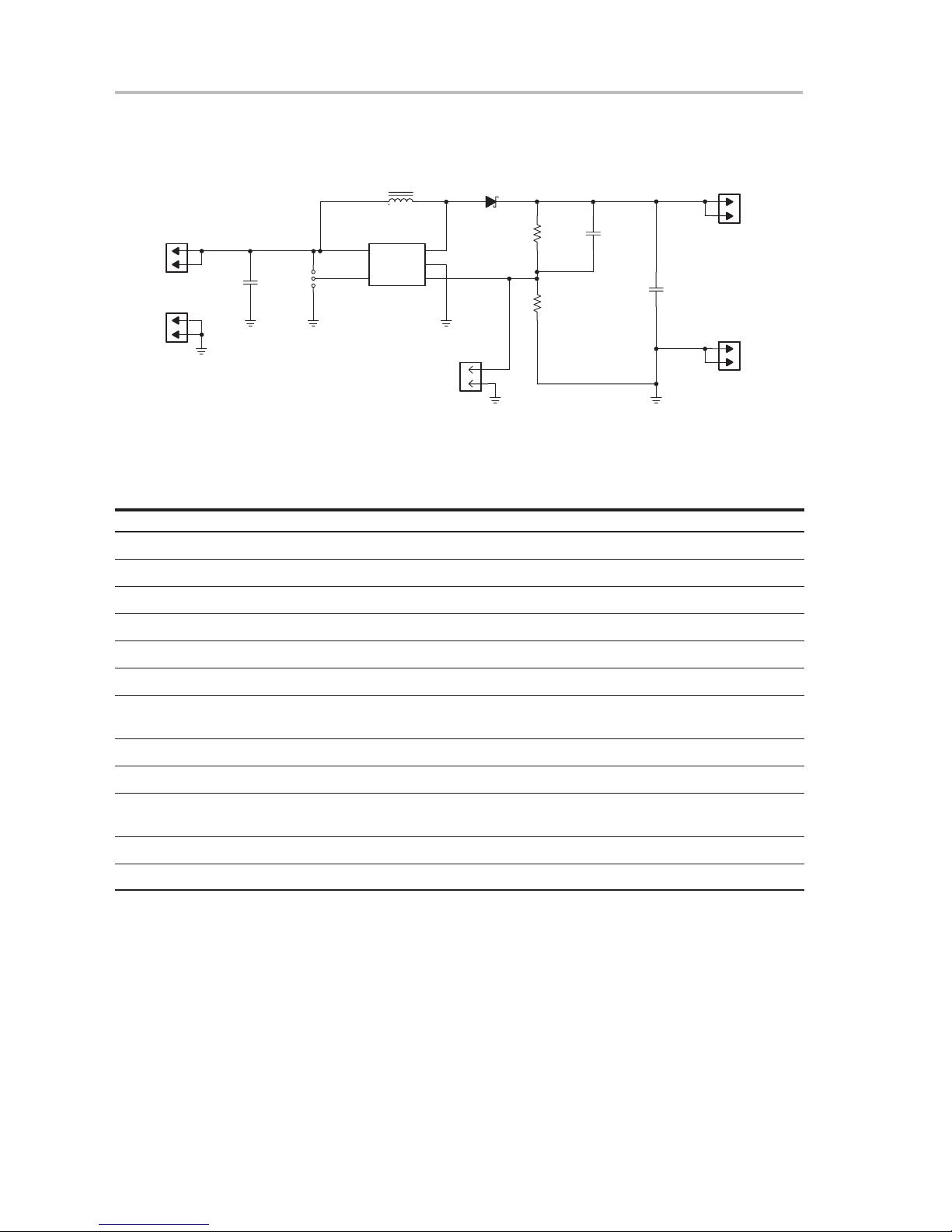
Figure 4−1.TPS61040EVM−001 Schematic
GND
L1
10 µH
U1
1
TPS61040DBV
5
VIN
GND
4
EN
SW
1
2
3
FB
Adjust
J1
1
V
I
2
JP1
C1
J2
1
2
4.7 µF
D1
MBR0530
J3
1
2
R1
2.21 MΩ
R2
162 kΩ
C2
22 pF
C3
1 µF
J5
1
V
O
2
J4
1
GND
2
4.2 Bill of Materials
Table 4−1.TPS61040EVM−001 Bill of Materials
Reference Description Size Qty. MFG Part #
C1 Capacitor, ceramic, 4.7 µF, 6.3 V, X5R, 15% 0805 1 Murata GRM21B60J475KA11
C2 Capacitor, ceramic, 22 pF, 50 V, C0G, 5% 0603 1 Murata GRM1885C1H220JZ01
C3 Capacitor, ceramic, 1 µF, 25 V, X7R, 10% 1206 1 Murata GRM31MR7E105KC01
D1 Diode, Schottky 0.5 A 30 V SOD−123 1 On Semi MBR0530T1
J1 − J5 Header, 2-pin, 100-mil spacing (36-pin strip) 0.1 x 2” 5 Sullins PTC36SAAN
JP1 Header, 3-pin, 100-mil spacing (36-pin strip) 0.1 x 3” 1 Sullins PTC36SAAN
L1 Inductor, SMT, 10 µH, 0.76 A, 0.23 Ω 0.15 x
1 Sumida CR32−100
0.162
R1 Resistor, chip, 2.21 MΩ, 1/16 W, 1% 0603 1 Standard Standard
R2 Resistor, chip, 162 kΩ, 1/16 W, 1% 0603 1 Standard Standard
U1 IC, high efficiency boost converter SOT23−5
1 TI TPS61040DBV
(DBV)
PCB, 1.5’ x 1” x 0.062” 1 Any SLVP209
Shunts, 100-mil, black 0.1 mm 1 3M 929950-00
4-2
Schematic and Bill of Materials
 Loading...