

Datasheet TPS61010, TPS61011, TPS61012, TPS61013, TPS61014 Datasheet (TEXAS INSTRUMENTS)
...Page 1
DRC
DGS
www.ti.com
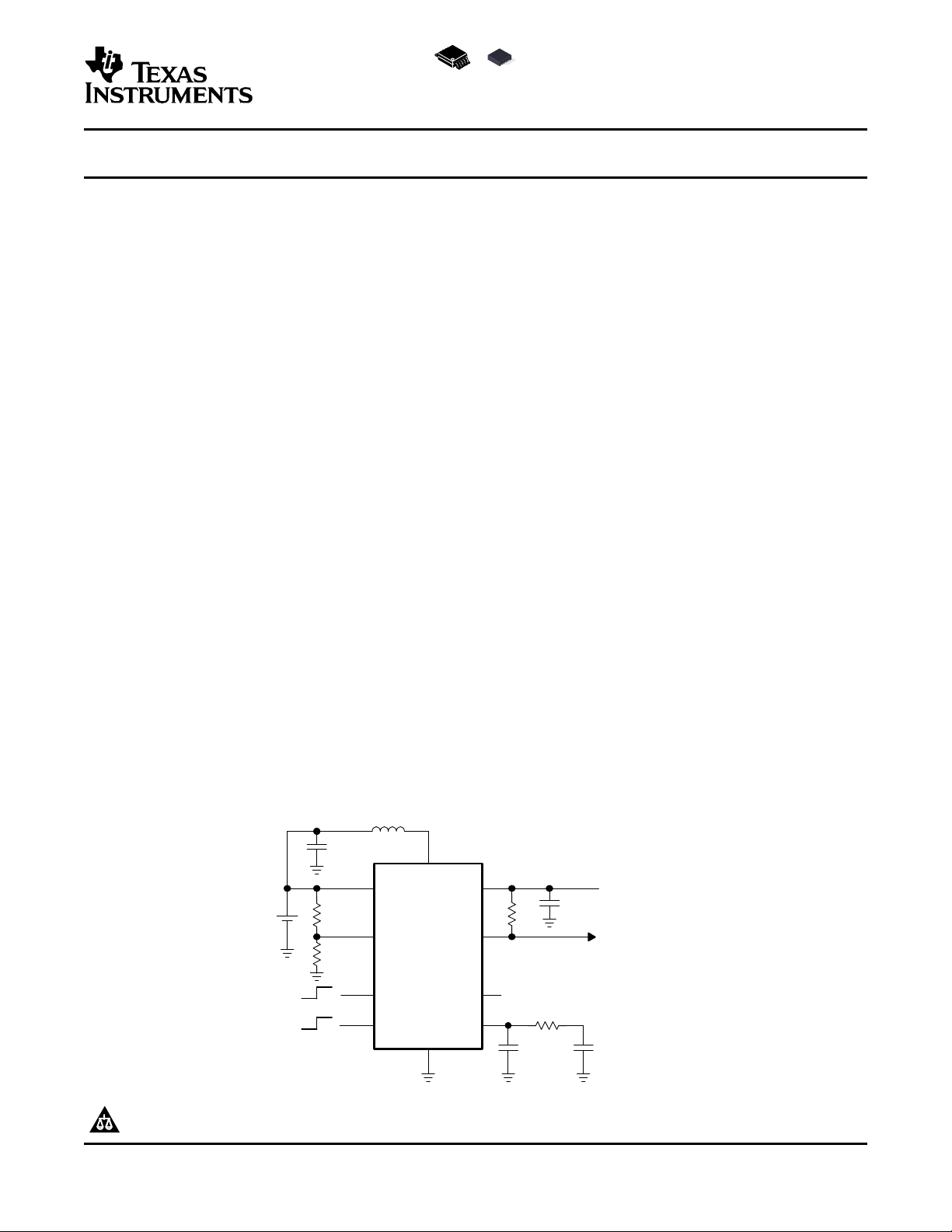
VBAT
LBI
EN
ADEN
VOUT
LBO
FB
COMP
SW
GND
C
IN
10 Fm
L1
10 Hm
R3
C
OUT
22 Fm
C
C1
10 pF
C
C2
10 nF
R
C
100 kW
6
9
1
8
4
2
3
10
5
7
OFF
ON
OFF
ON
VOUT = 3.3 V
Low Battery
Warning
TPS61016
R1
R2
HIGH-EFFICIENCY, 1-CELL AND 2-CELL BOOST CONVERTERS
TPS61010, TPS61011
TPS61012, TPS61013
TPS61014, TPS61015, TPS61016
SLVS314D – SEPTEMBER 2000 – REVISED JUNE 2005
FEATURES
• Integrated Synchronous Rectifier for Highest
Power Conversion Efficiency (>95%)
• Start-Up Into Full Load With Supply Voltages
as Low as 0.9 V, Operating Down to 0.8 V
• 200-mA Output Current From 0.9-V Supply
• Powersave-Mode for Improved Efficiency at
Low Output Currents
• Autodischarge Allows to Discharge Output
Capacitor During Shutdown
• Device Quiescent Current Less Than 50 µ A
• Ease-of-Use Through Isolation of Load From
Battery During Shutdown of Converter
• Integrated Antiringing Switch Across Inductor
• Integrated Low Battery Comparator
• Micro-Small 10-Pin MSOP or 3 mm x 3 mm
QFN Package
• EVM Available (TPS6101xEVM-157)
APPLICATIONS
• All Single- or Dual-Cell Battery Operated Prod-
ucts Like Internet Audio Players, Pager, Portable Medical Diagnostic Equipment, Remote
Control, Wireless Headsets
DESCRIPTION
The TPS6101x devices are boost converters intended
for systems that are typically operated from a singleor dual-cell nickel-cadmium (NiCd), nickel-metal hydride (NiMH), or alkaline battery.
The converter output voltage can be adjusted from
1.5 V to a maximum of 3.3 V, by an external resistor
divider or, is fixed internally on the chip. The devices
provide an output current of 200 mA with a supply
voltage of only 0.9 V. The converter starts up into a
full load with a supply voltage of only 0.9 V and stays
in operation with supply voltages down to 0.8 V.
The converter is based on a fixed frequency, current
mode, pulse-width-modulation (PWM) controller that
goes automatically into power save mode at light
load. It uses a built-in synchronous rectifier, so, no
external Schottky diode is required and the system
efficiency is improved. The current through the switch
is limited to a maximum value of 1300 mA. The
converter can be disabled to minimize battery drain.
During shutdown, the load is completely isolated from
the battery.
An autodischarge function allows discharging the
output capacitor during shutdown mode. This is
especially useful when a microcontroller or memory is
supplied, where residual voltage across the output
capacitor can cause malfunction of the applications.
When programming the ADEN-pin, the autodischarge
function can be disabled. A low-EMI mode is implemented to reduce interference and radiated electromagnetic energy when the converter enters the
discontinuous conduction mode. The device is packaged in the micro-small space saving 10-pin MSOP
package. The TPS61010 is also available in a 3 mm
x 3 mm 10-pin QFN package.
PRODUCTION DATA information is current as of publication date.
Products conform to specifications per the terms of the Texas
Instruments standard warranty. Production processing does not
necessarily include testing of all parameters.
Please be aware that an important notice concerning availability, standard warranty, and use in critical applications of Texas
Instruments semiconductor products and disclaimers thereto appears at the end of this data sheet.
Copyright © 2000–2005, Texas Instruments Incorporated
Page 2
www.ti.com
TPS61010, TPS61011
TPS61012, TPS61013
TPS61014, TPS61015, TPS61016
SLVS314D – SEPTEMBER 2000 – REVISED JUNE 2005
These devices have limited built-in ESD protection. The leads should be shorted together or the device placed in conductive foam
during storage or handling to prevent electrostatic damage to the MOS gates.
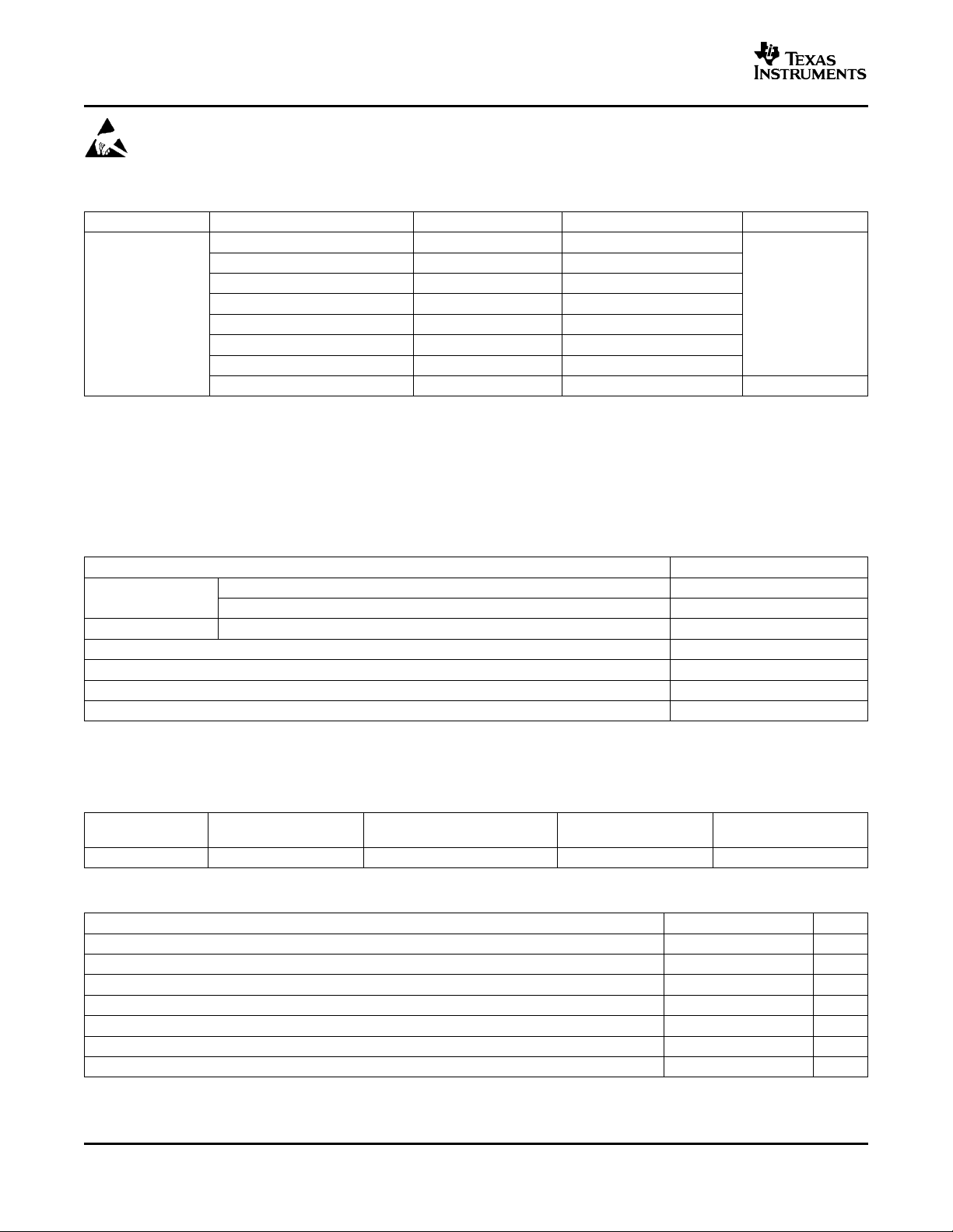
AVAILABLE OUTPUT VOLTAGE OPTIONS
T
A
-40 ° C to 85 ° C
(1) The DGS package and the DRC package are available taped and reeled. Add a R suffix to device type (e.g. TPS61010DGSR or
TPS61010DRCR) to order quantities of 3000 devices per reel. The DRC package is also available in mini-reels. Add a T suffix to the
device type (e.g. TPS61010DRCT) to order quantities of 250 devices per reel.
(2) For the most current package and ordering information, see the Package Option Addendum at the end of this document, or see the TI
Web site at www.ti.com .
OUTPUT VOLTAGE PART NUMBER
Adjustable from 1.5 V to 3.3 V TPS61010DGS AIP
1.5 V TPS61011DGS AIQ
1.8 V TPS61012DGS AIR
2.5 V TPS61013DGS AIS 10-Pin MSOP
2.8 V TPS61014DGS AIT
3.0 V TPS61015DGS AIU
3.3 V TPS61016DGS AIV
Adjustable from 1.5 V to 3.3 V TPS61010DRC AYA 10-Pin QFN
(1)
MARKING DGS PACKAGE PACKAGE
(2)
ABSOLUTE MAXIMUM RATINGS
over operating free-air temperature range (unless otherwise noted)
Input voltage range: VBAT, VOUT, EN, LBI, FB, ADEN -0.3 V to 3.6 V
SW -0.3 V to 7 V
Voltage range: LBO, COMP -0.3 V to 3.6 V
Operating free-air temperature range, T
Maximum junction temperature, T
Storage temperature range, T
Lead temperature 1,6 mm (1/16 inch) from case for 10s 260 ° C
(1) Stresses beyond those listed under "absolute maximum ratings" may cause permanent damage to the device. These are stress ratings
only, and functional operation of the device at these or any other conditions beyond those indicated under "recommended operating
conditions" is not implied. Exposure to absolute-maximum-rated conditions for extended periods may affect device reliability.
stg
A
J
DISSIPATION RATING TABLE
PACKAGE
DGS 424 mW 3.4 mW/ ° C 271 mW 220 mW
TA<25 ° C DERATING FACTOR TA= 70 ° C TA= 85 ° C
POWER RATING ABOVE TA= 25 ° C POWER RATING POWER RATING
(1)
UNIT
-40 ° C to 85 ° C
150 ° C
-65 ° C to 150 ° C
RECOMMENDED OPERATING CONDITIONS
MIN NOM MAX UNIT
Supply voltage at VBAT, V
Maximum output current at VIN = 1.2 V, I
Maximum output current at VIN = 2.4 V, I
Inductor, L1 10 33 µH
Input capacitor, C
Output capacitor, C
Operating virtual junction temperature, T
I
I
O
O
o
J
0.8 VOUT V
100 mA
200 mA
10 µF
10 22 47 µF
-40 125 ° C
2
Page 3
www.ti.com
TPS61010, TPS61011
TPS61012, TPS61013
TPS61014, TPS61015, TPS61016
SLVS314D – SEPTEMBER 2000 – REVISED JUNE 2005
ELECTRICAL CHARACTERISTICS
over recommended operating free-air temperature range, VBAT = 1.2 V, EN = VBAT (unless otherwise noted)
PARAMETER TEST CONDITIONS MIN TYP MAX UNIT
Minimum input voltage for
V
start-up
I
Input voltage once started IO= 100 mA 0.8
Programmable output
voltage range
V
O
Output voltage
I
O
I
(SW)
V
Maximum continuous output
current
Switch current limit A
Feedback voltage 480 500 520 mV
(FB)
f Oscillator frequency 420 500 780 kHz
D Maximum duty cycle 85%
r
DS(on)
r
DS(on)
NMOS switch on-resistance 0.37 0.51
PMOS switch on-resistance 0.45 0.54
NMOS switch on-resistance 0.2 0.37
PMOS switch on-resistance 0.3 0.45
Line regulation
Load regulation
(1)
(1)
Autodischarge switch
resistance
Residual output voltage
after autodischarge
V
LBI voltage threshold
IL
LBI input hysteresis 10 mv
LBI input current 0.01 0.03
V
LBO output low voltage V
OL
LBO output leakage current V
IL
FB input bias current
(TPS61010 only)
EN and ADEN input low
voltage
I
(FB)
V
(1) Line and load regulation is measured as a percentage deviation from the nominal value (i.e., as percentage deviation from the nominal
output voltage). For line regulation, x %/V stands for ± x% change of the nominal output voltage per 1-V change on the input/supply
voltage. For load regulation, y% stands for ± y% change of the nominal output voltage per the specified current change.
(2) For proper operation the voltage at LBI may not exceed the voltage at V
RL= 33 Ω 0.85 0.9
RL= 3 k Ω , TA= 25 ° C 0.8 V
TPS61010, I
= 100 mA 1.5 3.3 V
OUT
TPS61011, 0.8 V < VI< VO, IO= 0 to 100 mA 1.45 1.5 1.55
TPS61012, 0.8 V < VI< VO, IO= 0 to 100 mA 1.74 1.8 1.86
TPS61013, 0.8 V < VI< VO, IO= 0 to 100 mA 2.42 2.5 2.58 V
TPS61013, 1.6 V < VI< VO, IO= 0 to 200 mA 2.42 2.5 2.58 V
TPS61014, 0.8 V < VI< VO, IO= 0 to 100 mA 2.72 2.8 2.88 V
TPS61014, 1.6 V < VI< VO, IO= 0 to 200 mA 2.72 2.8 2.88 V
TPS61015, 0.8 V < VI< VO, IO= 0 to 100 mA 2.9 3.0 3.1 V
TPS61015, 1.6 V < VI< VO, IO= 0 to 200 mA 2.9 3.0 3.1 V
TPS61016, 0.8 V < VI< VO, IO= 0 to 100 mA 3.2 3.3 3.4 V
TPS61016, 1.6 V < VI< VO, IO= 0 to 200 mA 3.2 3.3 3.4 V
VI> 0.8 V 100
VI> 1.8 V 250
TPS61011, once started 0.39 0.48
TPS61012, once started 0.54 0.56
TPS61013, once started 0.85 0.93
TPS61014, once started 0.95 1.01
TPS61015, once started 1 1.06
TPS61016, once started 1.07 1.13
VO= 1.5 V Ω
VO= 3.3 V Ω
VI= 1.2 V to 1.4 V, IO= 100 mA 0.3
VI= 1.2 V; IO= 50 mA to 100 mA 0.1
300 400 Ω
ADEN = VBAT; EN = GND 0.4 V
(2)
V
voltage decreasing 480 500 520 mV
(LBI)
= 0 V, VO= 3.3 V, I
(LBI)
= 650 mV, V
(LBI)
V
= 500 mV 0.01 0.03
(FB)
0.8 V < V
BAT
(LBO)
< 3.3 V 0.2 × VBAT V
= 10 µA 0.04 0.2 V
(OL)
= V
O
.
BAT
0.03 µA
V
mA
%/V
3
Page 4
www.ti.com
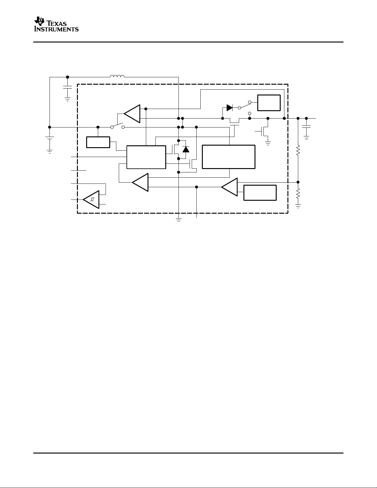
_
+
UVLO
Control Logic
Oscillator
Gate Drive
Current Sense,
Current Limit, Slope
Compensation
_
+
Antiringing
Comparator
and Switch
_
+
Bandgap
Reference
Bias
Control
ADEN
Error
Amplifier
_
+
C
OUT
VOUT
FB
COMP
GND
SW
L1
C
IN
VBAT
EN
ADEN
LBI
LBO
ADEN
VREF
Error
Comparator
TPS61010, TPS61011
TPS61012, TPS61013
TPS61014, TPS61015, TPS61016
SLVS314D – SEPTEMBER 2000 – REVISED JUNE 2005
ELECTRICAL CHARACTERISTICS (continued)
over recommended operating free-air temperature range, VBAT = 1.2 V, EN = VBAT (unless otherwise noted)
PARAMETER TEST CONDITIONS MIN TYP MAX UNIT
V
I
q
I
off
fixed output voltage versions TPS61011 to TPS61016
EN and ADEN input high
IH
voltage
EN and ADEN input current EN and ADEN = GND or VBAT 0.01 0.03 µA
Quiescent current into pins
VBAT/SW and VOUT
Shutdown current from
power source
0.8 V < V
IL= 0 mA, V
V
= 0 V, ADEN = VBAT, TA= 25 ° C 1 3 µA
EN
< 3.3 V 0.8 × VBAT V
BAT
= V
EN
I
VBAT/SW 31 46
V
O
5 8
FUNCTIONAL BLOCK DIAGRAMS
µA
4
Page 5
www.ti.com
_
+
UVLO
Control Logic
Oscillator
Gate Drive
Current Sense,
Current Limit, Slope
Compensation
_
+
Antiringing
Comparator
and Switch
_
+
Bandgap
Reference
Bias
Control
ADEN
Error
Amplifier
_
+
C
OUT
VOUT
FB
COMP
GND
SW
L1
C
IN
VBAT
EN
ADEN
LBI
LBO
ADEN
VREF
Error
Comparator
FUNCTIONAL BLOCK DIAGRAMS (continued)
adjustable output voltage version TPS61010
TPS61010, TPS61011
TPS61012, TPS61013
TPS61014, TPS61015, TPS61016
SLVS314D – SEPTEMBER 2000 – REVISED JUNE 2005
5
Page 6
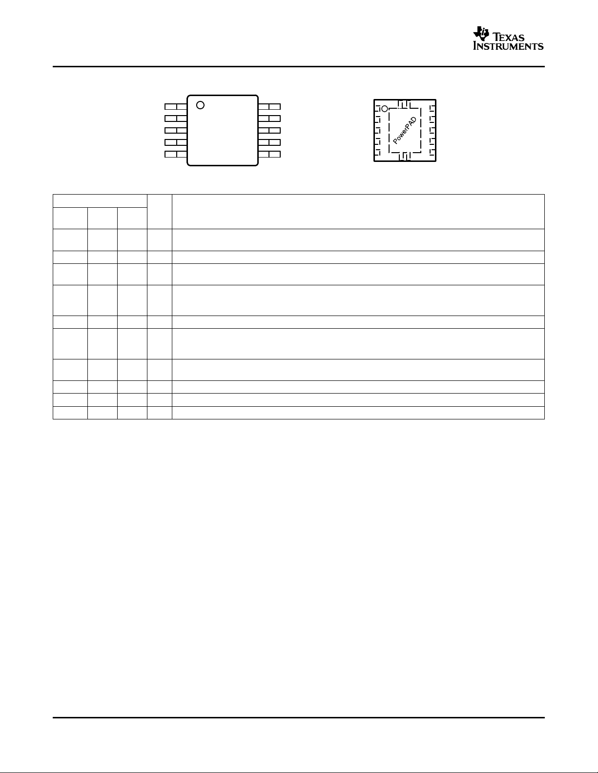
www.ti.com
DGS
(TOP VIEW)
DRC
(TOP VIEW)
1
2
3
4
5
10
9
8
7
6
EN
COMP
FB
GND
VOUT
LBO
LBI
ADEN
SW
VBAT
FB
GND
VOUT
VBAT
LBI
COMP
SW
ADEN
EN
LBO
TPS61010, TPS61011
TPS61012, TPS61013
TPS61014, TPS61015, TPS61016
SLVS314D – SEPTEMBER 2000 – REVISED JUNE 2005
Terminal Functions
Terminal
Name
ADEN 8 8 I
COMP 2 2 I Compensation of error amplifier. Connect an R/C/C network to set frequency response of control loop.
EN 1
FB 3 3 I depending on the output voltage divider connected there. For the fixed output voltage versions, leave
GND 4 4 Ground
LBI 9 9 I below the threshold of 500 mV. Connect LBI to GND or VBAT if the low-battery detector function is not
LBO 10 10 O
SW 7 7 I Switch input pin. The inductor is connected to this pin.
VOUT 5 5 O Output voltage. Internal resistor divider sets regulated output voltage in fixed output voltage versions.
VBAT 6 6 I Supply pin
DRG DRC
No. No.
1 I Chip-enable input. The converter is switched on if this pin is set high, it is switched off if this pin is
I/O Description
Autodischarge input. The autodischarge function is enabled if this pin is connected to VBAT, it is disabled
if ADEN is tied to GND.
connected to GND.
Feedback input for adjustable output voltage version TPS61010. Output voltage is programmed
FB-pin unconnected.
Low-battery detector input. A low battery warning is generated at LBO when the voltage on LBI drops
used. Do not leave this pin floating.
Open-drain low-battery detector output. This pin is pulled low if the voltage on LBI drops below the
threshold of 500 mV. A pullup resistor must be connected between LBO and VOUT.
DETAILED DESCRIPTION
Controller Circuit
The device is based on a current-mode control topology using a constant frequency pulse-width modulator to
regulate the output voltage. The controller limits the current through the power switch on a pulse by pulse basis.
The current-sensing circuit is integrated in the device, therefore, no additional components are required. Due to
the nature of the boost converter topology used here, the peak switch current is the same as the peak inductor
current, which will be limited by the integrated current limiting circuits under normal operating conditions.
The control loop must be externally compensated with an R-C-C network connected to the COMP-pin.
Synchronous Rectifier
The device integrates an N-channel and a P-channel MOSFET transistor to realize a synchronous rectifier. There
is no additional Schottky diode required. Because the device uses a integrated low r
rectification, the power conversion efficiency reaches 95%.
A special circuit is applied to disconnect the load from the input during shutdown of the converter. In conventional
synchronous rectifier circuits, the backgate diode of the high-side PMOS is forward biased in shutdown and
allows current flowing from the battery to the output. This device, however, uses a special circuit to disconnect
the backgate diode of the high-side PMOS and so, disconnects the output circuitry from the source when the
regulator is not enabled (EN = low).
The benefit of this feature for the system design engineer, is that the battery is not depleted during shutdown of
the converter. So, no additional effort has to be made by the system designer to ensure disconnection of the
battery from the output of the converter. Therefore, design performance will be increased without additional costs
and board space.
6
DS(on)
PMOS switch for
Page 7

www.ti.com
TPS61010, TPS61011
TPS61012, TPS61013
TPS61014, TPS61015, TPS61016
SLVS314D – SEPTEMBER 2000 – REVISED JUNE 2005
DETAILED DESCRIPTION (continued)
Power-Save Mode
The TPS61010 is designed for high efficiency over a wide output current range. Even at light loads, the efficiency
stays high because the switching losses of the converter are minimized by effectively reducing the switching
frequency. The controller enters a powersave-mode if certain conditions are met. In this mode, the controller only
switches on the transistor if the output voltage trips below a set threshold voltage. It ramps up the output voltage
with one or several pulses, and goes again into powersave-mode once the output voltage exceeds a set
threshold voltage.
Device Enable
The device is shut down when EN is set to GND. In this mode, the regulator stops switching, all internal control
circuitry including the low-battery comparator, is switched off, and the load is disconnected from the input (as
described above in the synchronous rectifier section). This also means that the output voltage may drop below
the input voltage during shutdown.
The device is put into operation when EN is set high. During start-up of the converter, the duty cycle is limited in
order to avoid high peak currents drawn from the battery. The limit is set internally by the current limit circuit and
is proportional to the voltage on the COMP-pin.
Under-Voltage Lockout
An under-voltage lockout function prevents the device from starting up if the supply voltage on VBAT is lower
than approximately 0.7 V. This under-voltage lockout function is implemented in order to prevent the
malfunctioning of the converter. When in operation and the battery is being discharged, the device will
automatically enter the shutdown mode if the voltage on VBAT drops below approximately 0.7 V.
Autodischarge
The autodischarge function is useful for applications where the supply voltage of a µ C, µ P, or memory has to be
removed during shutdown in order to ensure a defined state of the system.
The autodischarge function is enabled when the ADEN is set high, and is disabled when the ADEN is set to
GND. When the autodischarge function is enabled, the output capacitor will be discharged after the device is
shut down by setting EN to GND. The capacitors connected to the output are discharged by an integrated switch
of 300 Ω , hence the discharge time depends on the total output capacitance. The residual voltage on VOUT is
less than 0.4 V after autodischarge.
Low-Battery Detector Circuit (LBI and LBO)
The low-battery detector circuit is typically used to supervise the battery voltage and to generate an error flag
when the battery voltage drops below a user-set threshold voltage. The function is active only when the device is
enabled. When the device is disabled, the LBO-pin is high impedance. The LBO-pin goes active low when the
voltage on the LBI-pin decreases below the set threshold voltage of 500 mV ± 15 mV, which is equal to the
internal reference voltage. The battery voltage, at which the detection circuit switches, can be programmed with a
resistive divider connected to the LBI-pin. The resistive divider scales down the battery voltage to a voltage level
of 500 mV, which is then compared to the LBI threshold voltage. The LBI-pin has a built-in hysteresis of 10 mV.
See the application section for more details about the programming of the LBI-threshold.
If the low-battery detection circuit is not used, the LBI-pin should be connected to GND (or to VBAT) and the
LBO-pin can be left unconnected. Do not let the LBI-pin float.
Antiringing Switch
The device integrates a circuit that removes the ringing that typically appears on the SW-node when the
converter enters the discontinuous current mode. In this case, the current through the inductor ramps to zero and
the integrated PMOS switch turns off to prevent a reverse current from the output capacitors back to the battery.
Due to remaining energy that is stored in parasitic components of the semiconductors and the inductor, a ringing
on the SW pin is induced. The integrated antiringing switch clamps this voltage internally to V
dampens this ringing.
and therefore,
BAT
7
Page 8
www.ti.com
VBAT
LBI
ADEN
EN
VOUT
LBO
FB
COMP
SW
GND
C
IN
10 µF
L1
10 µH
R3
C
OUT
22 µF
C
C1
10 pF
C
C2
10 nF
R
C
100 kΩ
6
9
8
1
4
2
3
10
5
7
OFF
ON
VOUT = 3.3 V
Low Battery Warning
TPS61016
R1
R2
List of Components:
IC1: Only Fixed Output Versions
(Unless Otherwise Noted)
L1: SUMIDA CDRH6D38 – 100
CIN: X7R/X5R Ceramic
C
OUT
: X7R/X5R Ceramic
TPS61010, TPS61011
TPS61012, TPS61013
TPS61014, TPS61015, TPS61016
SLVS314D – SEPTEMBER 2000 – REVISED JUNE 2005
DETAILED DESCRIPTION (continued)
Adjustable Output Voltage
The devices with fixed output voltages are trimmed to operate with an output voltage accuracy of ± 3%.
The accuracy of the adjustable version is determined by the accuracy of the internal voltage reference, the
controller topology, and the accuracy of the external resistor. The reference voltage has an accuracy of ± 4% over
line, load, and temperature. The controller switches between fixed frequency and pulse-skip mode, depending on
load current. This adds an offset to the output voltage that is equivalent to 1% of VO. The tolerance of the
resistors in the feedback divider determine the total system accuracy.
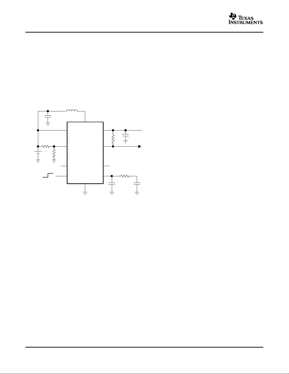
Parameter Measurement Information
Figure 1. Circuit Used for Typical Characteristics Measurements
8
Page 9
www.ti.com
TPS61010, TPS61011
TPS61012, TPS61013
TPS61014, TPS61015, TPS61016
SLVS314D – SEPTEMBER 2000 – REVISED JUNE 2005
Typical Characteristics
Table of Graphs
Maximum output current
Efficiency
Output voltage vs Output current TPS61013 12
Minimum supply start-up voltage vs Load resistance 14
No-load supply current vs Input voltage 15
Shutdown supply current vs Input voltage 16
Switch current limit vs Output voltage 17
Waveforms
vs Input voltage for VO= 2.5 V, 3.3 V 3
vs Input voltage for VO= 1.5 V, 1.8 V 4
vs Output current for VI= 1.2 VVO= 1.5 V, L1 = Sumida CDR74 - 10 µH 5
vs Output current for VI= 1.2 VVO= 2.5 V, L1 = Sumida CDR74 - 10 µH 6
vs Output current for VIN = 1.2 VVO= 3.3 V, L1 = Sumida CDR74 - 10 µH 7
vs Output current for VI= 2.4 VVO= 3.3 V, L1 = Sumida CDR74 - 10 µH 8
vs Input voltage for IO= 10 mA, IO= 100 mA, IO= 200 mAVO= 3.3 V, L1 = 9
Sumida CDR74 - 10 µH
TPS61016, VBAT = 1.2 V, IO= 100 mA
Sumida CDRH6D38 - 10 µH
Sumida CDRH5D18 - 10 µH
Sumida CDRH74 - 10 µH
Sumida CDRH74B - 10 µH
Coilcraft DS 1608C - 10 µH
Coilcraft DO 1608C - 10 µH
Coilcraft DO 3308P - 10 µH 10
Coilcraft DS 3316 - 10 µH
Coiltronics UP1B - 10 µH
Coiltronics UP2B - 10 µH
Murata LQS66C - 10 µH
Murata LQN6C - 10 µH
TDK SLF 7045 - 10 µH
TDK SLF 7032 - 10 µH
vs Output current TPS61011 11
vs Output current TPS61016 13
Output voltage (ripple) in continuous modeInductor current 18
Output voltage (ripple) in discontinuous modeInductor current 19
Load transient response for output current step of 50 mA to 100 mA 20
Line transient response for supply voltage step from 1.08 V to 1.32 V at 21
IO= 100 mA
Converter start-up time after enable 22
FIGURE
9
Page 10

www.ti.com
0
0.2
0.4
0.6
0.8
1
1.2
1.4
0.5 1 1.5 2 2.5 3
VO = 2.5 V
VO = 3.3 V
Maximum Output Current − A
VI − Input Voltage − V
0
0.1
0.2
0.3
0.4
0.5
0.6
0.7
0.8
0.9
0.5 1 1.5 2
VO = 1.8 V
VO = 1.5 V
Maximum Output Current − A
VI − Input Voltage − V
IO − Output Current − mA
40
50
60
70
80
90
100
0.1 1 10 100 1000
Efficiency − %
VBAT = 1.2 V,
VO = 1.5 V
IO − Output Current − mA
40
50
60
70
80
90
100
0.1 1 10 100 1000
Efficiency − %
VBAT = 1.2 V,
VO = 2.5 V
TPS61010, TPS61011
TPS61012, TPS61013
TPS61014, TPS61015, TPS61016
SLVS314D – SEPTEMBER 2000 – REVISED JUNE 2005
TYPICAL CHARACTERISTICS
MAXIMUM OUTPUT CURRENT MAXIMUM OUTPUT CURRENT
OUTPUT CURRENT OUTPUT CURRENT
vs vs
INPUT VOLTAGE INPUT VOLTAGE
Figure 2. Figure 3.
EFFICIENCY EFFICIENCY
vs vs
10
Figure 4. Figure 5.
Page 11

www.ti.com
IO − Output Current − mA
40
50
60
70
80
90
100
0.1 1 10 100 1000
Efficiency − %
VBAT = 1.2 V,
VO = 3.3 V
IO − Output Current − mA
40
50
60
70
80
90
100
0.1 1 10 100 1000
Efficiency − %
VBAT = 2.4 V,
VO = 3.3 V
40
50
60
70
80
90
100
0.5 1 1.5 2 2.5 3 3.5
VO = 3.3 V
IO = 10 mA
IO = 100 mA
IO = 200 mA
Efficiency − %
VI − Input Voltage − V
83
84
85
86
87
88
89
90
91
Sumida CDRH6D38
CDRH5D18
CDRH74
CDR74B
Coilcraft DS1608C
DO1608C
DO3308P
DS3316
Coiltronics UP1B
UP2B
Murata LQS66C
LQN6C
TDK SLF7045
SLF7032
Efficiency − %
Inductor Type
VBAT = 1.2 V,
VO = 3.3 V,
IO = 100 mA
TYPICAL CHARACTERISTICS (continued)
TPS61010, TPS61011
TPS61012, TPS61013
TPS61014, TPS61015, TPS61016
SLVS314D – SEPTEMBER 2000 – REVISED JUNE 2005
EFFICIENCY EFFICIENCY
vs vs
OUTPUT CURRENT OUTPUT CURRENT
Figure 6. Figure 7.
EFFICIENCY EFFICIENCY
vs vs
INPUT VOLTAGE INDUCTOR TYPE
Figure 8. Figure 9.
11
Page 12

www.ti.com
2.25
2.50
2.75
0.1 1 10 100 1 A
− Output Voltage − V
IO − Output Current − mA
VBAT = 1.2 V
V
O
1.25
1.50
1.75
0.1 1 10 100 1 A
− Output Voltage − V
IO − Output Current − mA
VBAT = 1.2 V
V
O
0.7
0.8
0.9
1
1100
Minimum Startup Supply Voltage − V
Load Resistance − Ω
3
3.25
3.50
0.1 1 10 100 1 A
− Output Voltage − V
IO − Output Current − mA
VBAT = 1.2 V
V
O
TPS61010, TPS61011
TPS61012, TPS61013
TPS61014, TPS61015, TPS61016
SLVS314D – SEPTEMBER 2000 – REVISED JUNE 2005
TYPICAL CHARACTERISTICS (continued)
OUTPUT VOLTAGE OUTPUT VOLTAGE
OUTPUT CURRENT OUTPUT CURRENT
OUTPUT VOLTAGE MINIMUM START-UP SUPPLY VOLTAGE
OUTPUT CURRENT LOAD RESISTANCE
vs vs
Figure 10. Figure 11.
vs vs
Figure 12. Figure 13.
12
Page 13

www.ti.com
0
10
20
30
40
50
60
0.5 1 1.5 2 2.5 3 3.5
TA = 25°C
TA = −40°C
TA = 85°C
VI − Input Voltage − V
− No-Load Supply Current −I
CC
Aµ
0
1
2
3
4
5
6
0.5 1 1.5 2 2.5 3 3.5
TA = 85°C
TA = 25°C
TA = −40°C
− Shutdown Supply Current −
I
CC
Aµ
VI − Input Voltage − V
Output Voltage
20 mV/div, AC
Inductor Current
50 mA/div, AC
0 0.5 1 1.5 2 2.5 3 3.5 4 4.5 5
t − Time − µs
0
0.2
0.4
0.6
0.8
1
1.2
1.5 1.7 1.9 2.1 2.3 2.5 2.7 2.9 3.1 3.3
Switch Current Limit − A
VO − Output Voltage − V
TYPICAL CHARACTERISTICS (continued)
TPS61010, TPS61011
TPS61012, TPS61013
TPS61014, TPS61015, TPS61016
SLVS314D – SEPTEMBER 2000 – REVISED JUNE 2005
NO-LOAD SUPPLY CURRENT SHUTDOWN SUPPLY CURRENT
SWITCH CURRENT LIMIT OUTPUT VOLTAGE RIPPLE IN CONTINUOUS MODE
OUTPUT VOLTAGE
vs vs
INPUT VOLTAGE INPUT VOLTAGE
Figure 14. Figure 15.
vs
Figure 16. Figure 17.
13
Page 14

www.ti.com
0 1 2 3 4 5 6 7 8 9 10
Output Voltage
50 mV/div, AC
Output Current
50 mA/div, AC
t − Time − ms
0 0.1 0.2 0.3 0.4 0.5 0.6 0.7 0.8 0.9 1
Output Voltage
50 mV/div, AC
Inductor Current
50 mA/div, AC
t − Time − ms
0 1 2 3 4 5 6 7 8 9 10
Input Voltage
100 mV/div, AC
Output Voltage
50 mA/div, AC
t − Time − ms
Enable,
2 V/div,DC
V
(SW)
,
2 V/div,DC
Output Voltage,
1 V/div,DC
Input Current,
200 mA/div,DC
0 1 2 3 4 5 6 7 8 9 10
t − Time − ms
TPS61010, TPS61011
TPS61012, TPS61013
TPS61014, TPS61015, TPS61016
SLVS314D – SEPTEMBER 2000 – REVISED JUNE 2005
TYPICAL CHARACTERISTICS (continued)
OUTPUT VOLTAGE RIPPLE IN DISCONTINUOUS MODE LOAD TRANSIENT RESPONSE
Figure 18. Figure 19.
LINE TRANSIENT RESPONSE CONVERTER START-UP TIME AFTER ENABLE
Figure 20. Figure 21.
14
Page 15

www.ti.com
R3 R4
V
O
V
FB
–1 500 k
V
O
500 mV
–1
VBAT
LBI
EN
ADEN
VOUT
LBO
FB
COMP
SW
GND
C
IN
10 µF
10 V
L1
10 µH
R5
C
OUT
22 µF
10 V
C
C1
10 pF
C
C2
10 nF
R
C
6
9
1
8
4
2
3
10
5
7
VOUT = 3.3 V
Low Battery Warning
TPS61016
1 Cell
NiMH,
NiCd or
Alkaline
R1
R2
R3
100 kΩ
R4
TPS61010, TPS61011
TPS61012, TPS61013
TPS61014, TPS61015, TPS61016
SLVS314D – SEPTEMBER 2000 – REVISED JUNE 2005
DESIGN PROCEDURE
The TPS6101x boost converter family is intended for systems that are powered by a single-cell NiCd or NiMH
battery with a typical terminal voltage between 0.9 V to 1.6 V. It can also be used in systems that are powered by
two-cell NiCd or NiMH batteries with a typical stack voltage between 1.8 V and 3.2 V. Additionally, single- or
dual-cell, primary and secondary alkaline battery cells can be the power source in systems where the TPS6101x
is used.
Programming the TPS61010 Adjustable Output Voltage Device
The output voltage of the TPS61010 can be adjusted with an external resistor divider. The typical value of the
voltage on the FB pin is 500 mV in fixed frequency operation and 485 mV in the power-save operation mode.
The maximum allowed value for the output voltage is 3.3 V. The current through the resistive divider should be
about 100 times greater than the current into the FB pin. The typical current into the FB pin is 0.01 µA, and the
voltage across R4 is typically 500 mV. Based on those two values, the recommended value for R4 is in the range
of 500 k Ω in order to set the divider current at 1 µA. From that, the value of resistor R3, depending on the
needed output voltage (V
If, as an example, an output voltage of 2.5 V is needed, a 2-M Ω resistor should be chosen for R3.
), can be calculated using Equation 1 .
O
(1)
Figure 22. Typical Application Circuit for Adjustable Output Voltage Option
The output voltage of the adjustable output voltage version changes with the output current. Due to
device-internal ground shift, which is caused by the high switch current, the internal reference voltage and the
voltage on the FB pin increases with increasing output current. Since the output voltage follows the voltage on
the FB pin, the output voltage rises as well with a rate of 1 mV per 1-mA output current increase. Additionally,
when the converter goes into pulse-skip mode at output currents around 5 mA and lower, the output voltage
drops due to the hysteresis of the controller. This hysteresis is about 15 mV, measured on the FB pin.
programming the low battery comparator threshold voltage
The current through the resistive divider should be about 100 times greater than the current into the LBI pin. The
typical current into the LBI pin is 0.01 µA, the voltage across R2 is equal to the reference voltage that is
generated on-chip, which has a value of 500 mV ± 15 mV. The recommended value for R2 is therefore in the
range of 500 k Ω . From that, the value of resistor R1, depending on the desired minimum battery voltage V
can be calculated using Equation 2 .
,
BAT
15
Page 16

www.ti.com
R1 R2
V
BAT
V
REF
–1 500 k
V
BAT
500 mV
–1
IL I
OUT
V
O
V
BAT
0.8
L
V
BAT
V
OUT
V
BAT
I
L
ƒ V
OUT
TPS61010, TPS61011
TPS61012, TPS61013
TPS61014, TPS61015, TPS61016
SLVS314D – SEPTEMBER 2000 – REVISED JUNE 2005
For example, if the low-battery detection circuit should flag an error condition on the LBO output pin at a battery
voltage of 1 V, a resistor in the range of 500 k Ω should be chosen for R1. The output of the low battery
comparator is a simple open-drain output that goes active low if the battery voltage drops below the programmed
threshold voltage on LBI. The output requires a pullup resistor with a recommended value of 1 M Ω , and should
only be pulled up to the VO. If not used, the LBO pin can be left floating or tied to GND.
inductor selection
A boost converter normally requires two main passive components for storing energy during the conversion. A
boost inductor is required and a storage capacitor at the output. To select the boost inductor, it is recommended
to keep the possible peak inductor current below the current limit threshold of the power switch in the chosen
configuration. For example, the current limit threshold of the TPS61010's switch is 1100 mA at an output voltage
of 3.3 V. The highest peak current through the inductor and the switch depends on the output load, the input
(V
), and the output voltage (V
BAT
Equation 3 .
For example, for an output current of 100 mA at 3.3 V, at least 515-mA of current flows through the inductor at a
minimum input voltage of 0.8 V.
The second parameter for choosing the inductor is the desired current ripple in the inductor. Normally, it is
advisable to work with a ripple of less than 20% of the average inductor current. A smaller ripple reduces the
magnetic hysteresis losses in the inductor, as well as output voltage ripple and EMI. But in the same way,
regulation time at load changes rises. In addition, a larger inductor increases the total system costs.
With those parameters, it is possible to calculate the value for the inductor by using Equation 4 .
). Estimation of the maximum average inductor current can be done using
O
(2)
(3)
Parameter 7 is the switching frequency and ∆ ILis the ripple current in the inductor, i.e., 20% × IL.
In this example, the desired inductor has the value of 12 µH. With this calculated value and the calculated
currents, it is possible to choose a suitable inductor. Care must be taken that load transients and losses in the
circuit can lead to higher currents as estimated in Equation 3 . Also, the losses in the inductor caused by
magnetic hysteresis losses and copper losses are a major parameter for total circuit efficiency.
The following inductor series from different suppliers were tested. All work with the TPS6101x converter within
their specified parameters:
Table 1. Recommended Inductors
VENDOR RECOMMENDED INDUCTOR SERIES
Sumida Sumida CDR74B
Sumida CDRH74
Sumida CDRH5D18
Sumida CDRH6D38
Coilcraft Coilcraft DO 1608C
Coilcraft DS 1608C
Coilcraft DS 3316
Coilcraft DT D03308P
Coiltronics Coiltronics UP1B
Coiltronics UP2B
(4)
16
Page 17
www.ti.com
C
min
I
OUT
V
OUT
V
BAT
ƒ V V
OUT
V
ESR
I
OUT
R
ESR
R
C
100 kΩ
C
C1
10 pF
C
C2
10 nF
COMP
TPS61010, TPS61011
TPS61012, TPS61013
TPS61014, TPS61015, TPS61016
SLVS314D – SEPTEMBER 2000 – REVISED JUNE 2005
Table 1. Recommended Inductors (continued)
VENDOR RECOMMENDED INDUCTOR SERIES
Murata Murata LQS66C
Murata LQN6C
TDK TDK SLF 7045
TDK SLF 7032
capacitor selection
The major parameter necessary to define the output capacitor is the maximum allowed output voltage ripple of
the converter. This ripple is determined by two parameters of the capacitor, the capacitance and the ESR. It is
possible to calculate the minimum capacitance needed for the defined ripple, supposing that the ESR is zero, by
using Equation 5 .
Parameter f is the switching frequency and ∆ V is the maximum allowed ripple.
With a chosen ripple voltage of 15 mV, a minimum capacitance of 10 µF is needed. The total ripple is larger due
to the ESR of the output capacitor. This additional component of the ripple can be calculated using Equation 6 .
An additional ripple of 30 mV is the result of using a tantalum capacitor with a low ESR of 300 m Ω . The total
ripple is the sum of the ripple caused by the capacitance and the ripple caused by the ESR of the capacitor. In
this example, the total ripple is 45 mV. It is possible to improve the design by enlarging the capacitor or using
smaller capacitors in parallel to reduce the ESR or by using better capacitors with lower ESR, like ceramics. For
example, a 10 µF ceramic capacitor with an ESR of 50 m Ω is used on the evaluation module (EVM). Tradeoffs
must be made between performance and costs of the converter circuit.
A 10µF input capacitor is recommended to improve transient behavior of the regulator. A ceramic capacitor or a
tantalum capacitor with a 100 nF ceramic capacitor in parallel placed close to the IC is recommended.
(5)
(6)
Compensation of the Control Loop
An R/C/C network must be connected to the COMP pin in order to stabilize the control loop of the converter.
Both the pole generated by the inductor L1 and the zero caused by the ESR and capacitance of the output
capacitor must be compensated. The network shown in Figure 5 satisfies these requirements.
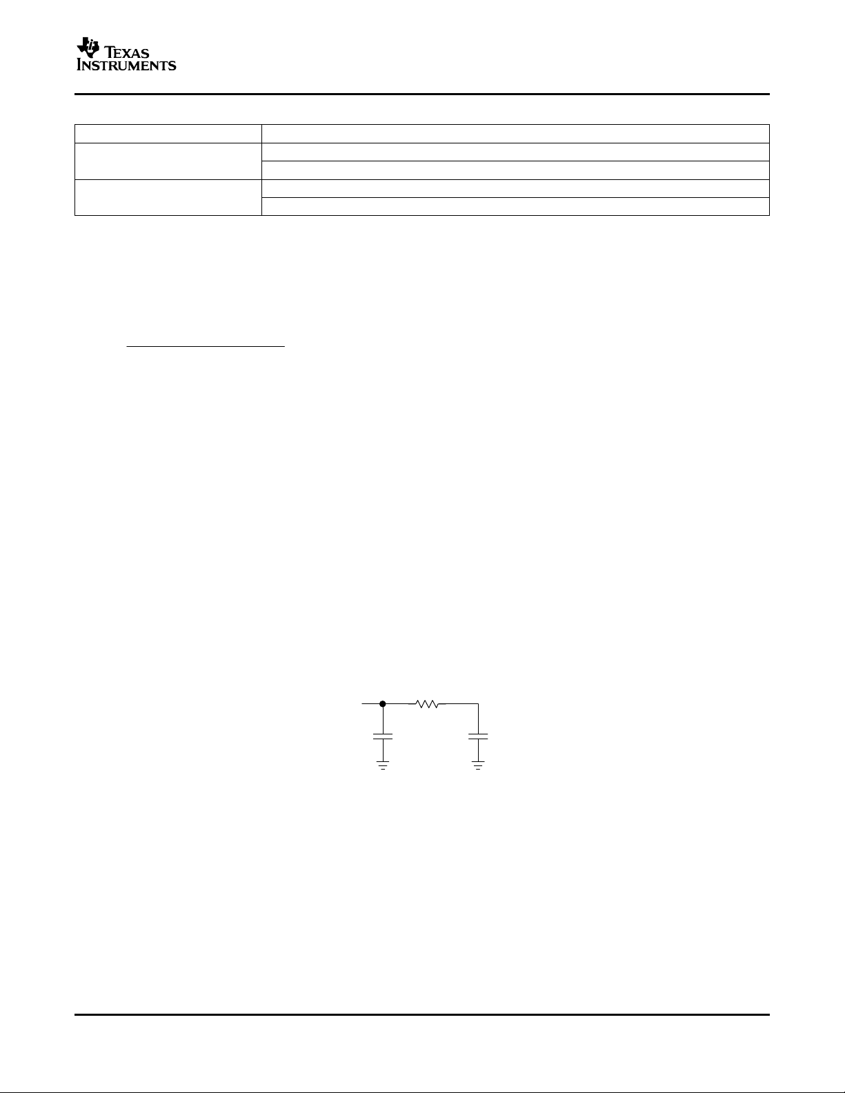
Figure 23. Compensation of Control Loop
Resistor R
should be chosen to 10 nF, or in other words, if the inductor is XXµH, the chosen compensation capacitor should
be XX nF, the same number value. The value of the compensation resistor is then chosen based on the
requirement to have a time constant of 1 ms, for the R/C network R
k Ω resistor should be chosen for RC.
Capacitor C
RC. Its value is calculated using Equation 7 .
and capacitor C
C
C1
depend on the chosen inductance. For a 10 µH inductor, the capacitance of C
C2
and C
C
, hence for a 33 nF capacitor, a 33
C2
depends on the ESR and capacitance value of the output capacitor, and on the value chosen for
C2
17
Page 18

www.ti.com
C
C1
C
OUT
ESR
COUT
R
C
SW
VBAT
LBI
ADEN
EN
VOUT
LBO
FB
COMP
GND
L1
R5
R6
C1
Battery
C2
R1
C3
LBO
R2
R3
C4
OUTPUT
U1
R4
TPS61010, TPS61011
TPS61012, TPS61013
TPS61014, TPS61015, TPS61016
SLVS314D – SEPTEMBER 2000 – REVISED JUNE 2005
(7)
For a selected output capacitor of 22 µF with an ESR of 0.2 Ω , an R
of 33 k Ω , the value of C
C
is in the range
C1
of 100 pF.
Table 2. Recommended Compensation Components
INDUCTOR[µH] RC[k Ω ] CC1[pF] CC2[nF]
33 22 0.2 33 120 33
22 22 0.3 47 150 22
10 22 0.4 100 100 10
10 10 0.1 100 10 10
OUTPUT CAPACITOR
CAPACITANCE[µF] ESR[ Ω ]
Layout Considerations
As for all switching power supplies, the layout is an important step in the design, especially at high peak currents
and high switching frequencies. If the layout is not carefully done, the regulator could show stability problems as
well as EMI problems.
Therefore, use wide and short traces for the main current path as indicated in bold in Figure 24 . The input
capacitor, output capacitor, and the inductor should be placed as close as possible to the IC. Use a common
ground node as shown in Figure 24 to minimize the effects of ground noise. The compensation circuit and the
feedback divider should be placed as close as possible to the IC. To layout the control ground, it is
recommended to use short traces as well, separated from the power ground traces. Connect both grounds close
to the ground pin of the IC as indicated in the layout diagram in Figure 24 . This avoids ground shift problems,
which can occur due to superimposition of power ground current and control ground current.
18
Figure 24. Layout Diagram
Page 19
www.ti.com
SW
VBAT
LBI
ADEN
EN
VOUT
LBO
FB
COMP
GND
L1
R5
R6
C1
Battery
C2
R1
C3
LBO
C5
OUTPUT
U1
R4
C4
List of Components:
U1 TPS6101 (1–6)
C1, C4, C5 10 µF X5R Ceramic,
TDK C3216X5R0J106
L1 10 µH
SUMIDA CDRH5D18–100
SW
VBAT
LBI
ADEN
EN
VOUT
LBO
FB
COMP
GND
L1
R5
R6
C1
Battery
C2
R1
C3
LBO
OUTPUT
U1
R4
C4
List of Components:
U1 TPS6101 (1–6)
C1 10 µF X5R Ceramic,
TDK C3216X5R0J106
C4 22 µF X5R Ceramic,
TDK C3225X5R0J226
L1 10 µH SUMIDA CDRH6D38
IOUT ≥ 250 mA
TPS61010, TPS61011
TPS61012, TPS61013
TPS61014, TPS61015, TPS61016
SLVS314D – SEPTEMBER 2000 – REVISED JUNE 2005
APPLICATION INFORMATION
Figure 25. 1,8 mm Maximum Height Power Supply With Single Battery Cell Input Using Low Profile
Components
Figure 26. 250-mA Power Supply With Two Battery Cell Input
19
Page 20

www.ti.com
SW
VBAT
LBI
ADEN
EN
VOUT
LBO
FB
COMP
GND
L1
R5
R6
C1
Battery
C2
R1
C3
LBO
3.3-V I/O Supply
U1
R4
C4
List of Components:
U1 TPS61016
U2 TPS76915
C1 10 µF X5R Ceramic,
TDK C3216X5R0J106
C4 22 µF X5R Ceramic,
TDK C3225X5R0J226
L1 10 µH SUMIDA CDRH6D38
U2
LDO
C6
1.5-V Core Supply
GND
SW
VBAT
LBI
ADEN
EN
VOUT
LBO
FB
COMP
GND
L1
R5
R6
C1
Battery
C2
R1
C3
LBO
U1
R4
C4
List of Components:
U1 TPS61016
DS1 BAT54S
C1 10 µF X5R Ceramic,
TDK C3216X5R0J106
C4 22 µF X5R Ceramic,
TDK C3225X5R0J226,
C6 1 µF X5R Ceramic,
C7 0.1 µF X5R Ceramic,
L1 10 µH SUMIDA CDRH6D38–100
GND
C7
DS1
C6
6-V/10-mA Aux Output
3.3-V/100-mA Main Output
TPS61010, TPS61011
TPS61012, TPS61013
TPS61014, TPS61015, TPS61016
SLVS314D – SEPTEMBER 2000 – REVISED JUNE 2005
APPLICATION INFORMATION (continued)
20
Figure 27. Dual Output Voltage Power Supply for DSPs
Figure 28. Power Supply With Auxiliary Positive Output Voltage
Page 21

www.ti.com
SW
VBAT
LBI
ADEN
EN
VOUT
LBO
FB
COMP
GND
L1
R5
R6
C1
Battery
C2
R1
C3
LBO
U1
R4
C4
List of Components:
U1 TPS61016
DS1 BAT54S
C1 10 µF X5R Ceramic,
TDK C3216X5R0J106
C4 22 µF X5R Ceramic,
TDK C3225X5R0J226,
C6 1 µF X5R Ceramic,
C7 0.1 µF X5R Ceramic,
L1 10 µH SUMIDA CDRH6D38–100
GND
DS1
C6
–2.7-V/10-mA Aux Output
3.3-V/100-mA Main Output
C7
GND
SW
VBAT
LBI
ADEN
EN
VOUT
LBO
FB
COMP
GND
L1
R5
R6
C1
C2
R1
C3
LBO
C5
OUTPUT
R4
C4
GND
R2
R3
J1
J2
INPUT
TPS6101x
APPLICATION INFORMATION (continued)
TPS61010, TPS61011
TPS61012, TPS61013
TPS61014, TPS61015, TPS61016
SLVS314D – SEPTEMBER 2000 – REVISED JUNE 2005
Figure 29. Power Supply With Auxiliary Negative Output Voltage
Figure 30. TPS6101x EVM Circuit Diagram
21
Page 22

www.ti.com
TPS61010, TPS61011
TPS61012, TPS61013
TPS61014, TPS61015, TPS61016
SLVS314D – SEPTEMBER 2000 – REVISED JUNE 2005
APPLICATION INFORMATION (continued)
Figure 31. TPS6101x EVM Component Placement (actual size: 55,9 mm x 40,6 mm)
Figure 32. TPS6101x EVM Top Layer Layout (actual size: 55,9 mm x 40,6 mm)
22
Page 23

www.ti.com
P
D(MAX)
T
J(MAX)
– T
A
R
JA
125°C 85°C
294°CW
136 mW
APPLICATION INFORMATION (continued)
TPS61010, TPS61011
TPS61012, TPS61013
TPS61014, TPS61015, TPS61016
SLVS314D – SEPTEMBER 2000 – REVISED JUNE 2005
Figure 33. TPS6101x EVM Bottom Layer Layout (actual size: 55,9 mm x 40,6 mm)
THERMAL INFORMATION
Implementation of integrated circuits in low-profile and fine-pitch surface-mount packages typically requires
special attention to power dissipation. Many system-dependent issues such as thermal coupling, airflow, added
heat sinks and convection surfaces, and the presence of other heat-generating components affect the
power-dissipation limits of a given component.
Three basic approaches for enhancing thermal performance are:
• Improving the power dissipation capability of the PWB design
• Improving the thermal coupling of the component to the PWB
• Introducing airflow in the system
The maximum junction temperature (T
MSOP package (DGS) is R
temperature (T
) of 85 ° C. Therefore, the maximum power dissipation is about 130 mW. More power can be
A
ΘJA
dissipated if the maximum ambient temperature of the application is lower.
) of the TPS6101x devices is 125 ° C. The thermal resistance of the 10-pin
J
= 294 ° C/W. Specified regulator operation is assured to a maximum ambient
(8)
23
Page 24

Page 25

Page 26

PACKAGE OPTION ADDENDUM
www.ti.com
PACKAGING INFORMATION
Orderable Device Status
TPS61010DGS ACTIVE MSOP DGS 10 80 Green (RoHS &
TPS61010DGSG4 ACTIVE MSOP DGS 10 80 Green (RoHS &
TPS61010DGSR ACTIVE MSOP DGS 10 2500 Green (RoHS &
TPS61010DGSRG4 ACTIVE MSOP DGS 10 2500 Green (RoHS &
TPS61010DRCR ACTIVE SON DRC 10 3000 Green (RoHS &
TPS61010DRCRG4 ACTIVE SON DRC 10 3000 Green (RoHS &
TPS61010DRCT PREVIEW SON DRC 10 250 TBD Call TI Call TI
TPS61011DGS ACTIVE MSOP DGS 10 80 Green (RoHS &
TPS61011DGSG4 ACTIVE MSOP DGS 10 80 Green (RoHS &
TPS61011DGSR ACTIVE MSOP DGS 10 2500 Green (RoHS &
TPS61011DGSRG4 ACTIVE MSOP DGS 10 2500 Green (RoHS &
TPS61012DGS ACTIVE MSOP DGS 10 80 Green (RoHS &
TPS61012DGSR ACTIVE MSOP DGS 10 2500 Green (RoHS &
TPS61012DGSRG4 ACTIVE MSOP DGS 10 Green (RoHS &
TPS61013DGS ACTIVE MSOP DGS 10 80 Green (RoHS &
TPS61013DGSR ACTIVE MSOP DGS 10 2500 Green (RoHS &
TPS61014DGS ACTIVE MSOP DGS 10 80 Green (RoHS &
TPS61014DGSR ACTIVE MSOP DGS 10 2500 Green (RoHS &
TPS61014DGSRG4 ACTIVE MSOP DGS 10 2500 Green (RoHS &
TPS61015DGS ACTIVE MSOP DGS 10 80 Green (RoHS &
TPS61015DGSG4 ACTIVE MSOP DGS 10 80 Green (RoHS &
TPS61015DGSR ACTIVE MSOP DGS 10 2500 Green (RoHS &
TPS61015DGSRG4 ACTIVE MSOP DGS 10 2500 Green (RoHS &
TPS61016DGS ACTIVE MSOP DGS 10 80 Green (RoHS &
TPS61016DGSG4 ACTIVE MSOP DGS 10 80 Green (RoHS &
(1)
Package
Type
Package
Drawing
Pins Package
Qty
Eco Plan
no Sb/Br)
no Sb/Br)
no Sb/Br)
no Sb/Br)
no Sb/Br)
no Sb/Br)
no Sb/Br)
no Sb/Br)
no Sb/Br)
no Sb/Br)
no Sb/Br)
no Sb/Br)
no Sb/Br)
no Sb/Br)
no Sb/Br)
no Sb/Br)
no Sb/Br)
no Sb/Br)
no Sb/Br)
no Sb/Br)
no Sb/Br)
no Sb/Br)
no Sb/Br)
no Sb/Br)
(2)
Lead/Ball Finish MSL Peak Temp
CU NIPDAU Level-1-260C-UNLIM
CU NIPDAU Level-1-260C-UNLIM
CU NIPDAU Level-1-260C-UNLIM
CU NIPDAU Level-1-260C-UNLIM
CU NIPDAU Level-2-260C-1 YEAR
CU NIPDAU Level-2-260C-1 YEAR
CU NIPDAU Level-1-260C-UNLIM
CU NIPDAU Level-1-260C-UNLIM
CU NIPDAU Level-1-260C-UNLIM
CU NIPDAU Level-1-260C-UNLIM
CU NIPDAU Level-1-260C-UNLIM
CU NIPDAU Level-1-260C-UNLIM
CU NIPDAU Level-1-260C-UNLIM
CU NIPDAU Level-1-260C-UNLIM
CU NIPDAU Level-1-260C-UNLIM
CU NIPDAU Level-1-260C-UNLIM
CU NIPDAU Level-1-260C-UNLIM
CU NIPDAU Level-1-260C-UNLIM
CU NIPDAU Level-1-260C-UNLIM
CU NIPDAU Level-1-260C-UNLIM
CU NIPDAU Level-1-260C-UNLIM
CU NIPDAU Level-1-260C-UNLIM
CU NIPDAU Level-1-260C-UNLIM
CU NIPDAU Level-1-260C-UNLIM
9-Aug-2005
(3)
Addendum-Page 1
Page 27

PACKAGE OPTION ADDENDUM
www.ti.com
Orderable Device Status
(1)
Package
Type
Package
Drawing
Pins Package
Qty
Eco Plan
(2)
TPS61016DGSR ACTIVE MSOP DGS 10 2500 Green (RoHS &
Lead/Ball Finish MSL Peak Temp
CU NIPDAU Level-1-260C-UNLIM
9-Aug-2005
(3)
no Sb/Br)
TPS61016DGSRG4 ACTIVE MSOP DGS 10 2500 Green (RoHS &
CU NIPDAU Level-1-260C-UNLIM
no Sb/Br)
(1)
The marketing status values are defined as follows:
ACTIVE: Product device recommended for new designs.
LIFEBUY: TI has announced that the device will be discontinued, and a lifetime-buy period is in effect.
NRND: Not recommended for new designs. Device is in production to support existing customers, but TI does not recommend using this part in
a new design.
PREVIEW: Device has been announced but is not in production. Samples may or may not be available.
OBSOLETE: TI has discontinued the production of the device.
(2)
Eco Plan - The planned eco-friendly classification: Pb-Free (RoHS) or Green (RoHS & no Sb/Br) - please check
http://www.ti.com/productcontent for the latest availability information and additional product content details.
TBD: The Pb-Free/Green conversion plan has not been defined.
Pb-Free (RoHS): TI's terms "Lead-Free" or "Pb-Free" mean semiconductor products that are compatible with the current RoHS requirements
for all 6 substances, including the requirement that lead not exceed 0.1% by weight in homogeneous materials. Where designed to be soldered
at high temperatures, TI Pb-Free products are suitable for use in specified lead-free processes.
Green (RoHS & no Sb/Br): TI defines "Green" to mean Pb-Free (RoHS compatible), and free of Bromine (Br) and Antimony (Sb) based flame
retardants (Br or Sb do not exceed 0.1% by weight in homogeneous material)
(3)
MSL, Peak Temp. -- The Moisture Sensitivity Level rating according to the JEDEC industry standard classifications, and peak solder
temperature.
Important Information and Disclaimer:The information provided on this page represents TI's knowledge and belief as of the date that it is
provided. TI bases its knowledge and belief on information provided by third parties, and makes no representation or warranty as to the
accuracy of such information. Efforts are underway to better integrate information from third parties. TI has taken and continues to take
reasonable steps to provide representative and accurate information but may not have conducted destructive testing or chemical analysis on
incoming materials and chemicals. TI and TI suppliers consider certain information to be proprietary, and thus CAS numbers and other limited
information may not be available for release.
In no event shall TI's liability arising out of such information exceed the total purchase price of the TI part(s) at issue in this document sold by TI
to Customer on an annual basis.
Addendum-Page 2
Page 28

Page 29

Page 30

IMPORTANT NOTICE
Texas Instruments Incorporated and its subsidiaries (TI) reserve the right to make corrections, modifications,
enhancements, improvements, and other changes to its products and services at any time and to discontinue
any product or service without notice. Customers should obtain the latest relevant information before placing
orders and should verify that such information is current and complete. All products are sold subject to TI’s terms
and conditions of sale supplied at the time of order acknowledgment.
TI warrants performance of its hardware products to the specifications applicable at the time of sale in
accordance with TI’s standard warranty. Testing and other quality control techniques are used to the extent TI
deems necessary to support this warranty . Except where mandated by government requirements, testing of all
parameters of each product is not necessarily performed.
TI assumes no liability for applications assistance or customer product design. Customers are responsible for
their products and applications using TI components. To minimize the risks associated with customer products
and applications, customers should provide adequate design and operating safeguards.
TI does not warrant or represent that any license, either express or implied, is granted under any TI patent right,
copyright, mask work right, or other TI intellectual property right relating to any combination, machine, or process
in which TI products or services are used. Information published by TI regarding third-party products or services
does not constitute a license from TI to use such products or services or a warranty or endorsement thereof.
Use of such information may require a license from a third party under the patents or other intellectual property
of the third party, or a license from TI under the patents or other intellectual property of TI.
Reproduction of information in TI data books or data sheets is permissible only if reproduction is without
alteration and is accompanied by all associated warranties, conditions, limitations, and notices. Reproduction
of this information with alteration is an unfair and deceptive business practice. TI is not responsible or liable for
such altered documentation.
Resale of TI products or services with statements different from or beyond the parameters stated by TI for that
product or service voids all express and any implied warranties for the associated TI product or service and
is an unfair and deceptive business practice. TI is not responsible or liable for any such statements.
Following are URLs where you can obtain information on other Texas Instruments products and application
solutions:
Products Applications
Amplifiers amplifier.ti.com Audio www.ti.com/audio
Data Converters dataconverter.ti.com Automotive www.ti.com/automotive
DSP dsp.ti.com Broadband www.ti.com/broadband
Interface interface.ti.com Digital Control www.ti.com/digitalcontrol
Logic logic.ti.com Military www.ti.com/military
Power Mgmt power.ti.com Optical Networking www.ti.com/opticalnetwork
Microcontrollers microcontroller.ti.com Security www.ti.com/security
Telephony www.ti.com/telephony
Video & Imaging www.ti.com/video
Wireless www.ti.com/wireless
Mailing Address: Texas Instruments
Post Office Box 655303 Dallas, Texas 75265
Copyright 2005, Texas Instruments Incorporated
 Loading...